EP2333592A2 - Rückbeleuchtungseinheit und Anzeigevorrichtung damit - Google Patents
Rückbeleuchtungseinheit und Anzeigevorrichtung damit Download PDFInfo
- Publication number
- EP2333592A2 EP2333592A2 EP10014623A EP10014623A EP2333592A2 EP 2333592 A2 EP2333592 A2 EP 2333592A2 EP 10014623 A EP10014623 A EP 10014623A EP 10014623 A EP10014623 A EP 10014623A EP 2333592 A2 EP2333592 A2 EP 2333592A2
- Authority
- EP
- European Patent Office
- Prior art keywords
- light
- guide plate
- substrate
- light source
- frame
- Prior art date
- Legal status (The legal status is an assumption and is not a legal conclusion. Google has not performed a legal analysis and makes no representation as to the accuracy of the status listed.)
- Withdrawn
Links
- 239000000758 substrate Substances 0.000 claims abstract description 80
- 239000004973 liquid crystal related substance Substances 0.000 claims abstract description 55
- 230000003287 optical effect Effects 0.000 claims description 11
- 230000005540 biological transmission Effects 0.000 claims description 6
- 239000000463 material Substances 0.000 description 9
- 238000002310 reflectometry Methods 0.000 description 7
- 238000000034 method Methods 0.000 description 6
- 230000000149 penetrating effect Effects 0.000 description 6
- 238000004519 manufacturing process Methods 0.000 description 5
- 239000011888 foil Substances 0.000 description 4
- 239000002184 metal Substances 0.000 description 4
- 238000007740 vapor deposition Methods 0.000 description 4
- 230000002708 enhancing effect Effects 0.000 description 3
- 238000012986 modification Methods 0.000 description 3
- 230000004048 modification Effects 0.000 description 3
- 239000003086 colorant Substances 0.000 description 2
- 238000004891 communication Methods 0.000 description 2
- 210000002858 crystal cell Anatomy 0.000 description 2
- 238000009792 diffusion process Methods 0.000 description 2
- 230000000694 effects Effects 0.000 description 2
- 230000001678 irradiating effect Effects 0.000 description 2
- 230000001788 irregular Effects 0.000 description 2
- NIXOWILDQLNWCW-UHFFFAOYSA-N acrylic acid group Chemical group C(C=C)(=O)O NIXOWILDQLNWCW-UHFFFAOYSA-N 0.000 description 1
- 238000009826 distribution Methods 0.000 description 1
- 239000011521 glass Substances 0.000 description 1
- 230000001902 propagating effect Effects 0.000 description 1
- 238000004904 shortening Methods 0.000 description 1
- 229920003002 synthetic resin Polymers 0.000 description 1
- 239000000057 synthetic resin Substances 0.000 description 1
- 239000002699 waste material Substances 0.000 description 1
Images






Classifications
-
- G—PHYSICS
- G02—OPTICS
- G02B—OPTICAL ELEMENTS, SYSTEMS OR APPARATUS
- G02B6/00—Light guides; Structural details of arrangements comprising light guides and other optical elements, e.g. couplings
- G02B6/0001—Light guides; Structural details of arrangements comprising light guides and other optical elements, e.g. couplings specially adapted for lighting devices or systems
- G02B6/0011—Light guides; Structural details of arrangements comprising light guides and other optical elements, e.g. couplings specially adapted for lighting devices or systems the light guides being planar or of plate-like form
- G02B6/0013—Means for improving the coupling-in of light from the light source into the light guide
- G02B6/0015—Means for improving the coupling-in of light from the light source into the light guide provided on the surface of the light guide or in the bulk of it
- G02B6/0018—Redirecting means on the surface of the light guide
-
- G—PHYSICS
- G02—OPTICS
- G02B—OPTICAL ELEMENTS, SYSTEMS OR APPARATUS
- G02B6/00—Light guides; Structural details of arrangements comprising light guides and other optical elements, e.g. couplings
- G02B6/0001—Light guides; Structural details of arrangements comprising light guides and other optical elements, e.g. couplings specially adapted for lighting devices or systems
- G02B6/0011—Light guides; Structural details of arrangements comprising light guides and other optical elements, e.g. couplings specially adapted for lighting devices or systems the light guides being planar or of plate-like form
- G02B6/0033—Means for improving the coupling-out of light from the light guide
- G02B6/005—Means for improving the coupling-out of light from the light guide provided by one optical element, or plurality thereof, placed on the light output side of the light guide
- G02B6/0055—Reflecting element, sheet or layer
-
- G—PHYSICS
- G02—OPTICS
- G02B—OPTICAL ELEMENTS, SYSTEMS OR APPARATUS
- G02B6/00—Light guides; Structural details of arrangements comprising light guides and other optical elements, e.g. couplings
- G02B6/0001—Light guides; Structural details of arrangements comprising light guides and other optical elements, e.g. couplings specially adapted for lighting devices or systems
- G02B6/0011—Light guides; Structural details of arrangements comprising light guides and other optical elements, e.g. couplings specially adapted for lighting devices or systems the light guides being planar or of plate-like form
- G02B6/0066—Light guides; Structural details of arrangements comprising light guides and other optical elements, e.g. couplings specially adapted for lighting devices or systems the light guides being planar or of plate-like form characterised by the light source being coupled to the light guide
- G02B6/0073—Light emitting diode [LED]
-
- G—PHYSICS
- G02—OPTICS
- G02B—OPTICAL ELEMENTS, SYSTEMS OR APPARATUS
- G02B6/00—Light guides; Structural details of arrangements comprising light guides and other optical elements, e.g. couplings
- G02B6/0001—Light guides; Structural details of arrangements comprising light guides and other optical elements, e.g. couplings specially adapted for lighting devices or systems
- G02B6/0011—Light guides; Structural details of arrangements comprising light guides and other optical elements, e.g. couplings specially adapted for lighting devices or systems the light guides being planar or of plate-like form
- G02B6/0081—Mechanical or electrical aspects of the light guide and light source in the lighting device peculiar to the adaptation to planar light guides, e.g. concerning packaging
- G02B6/0086—Positioning aspects
Definitions
- the present invention relates to a backlight unit for irradiating light from a light source on the rear surface of a liquid crystal panel through a light guide plate, and a display device using the same.
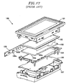
- a conventional display device 100 shown in Fig. 17 is used as a display device in, e.g., a programmable logic controller (PLC) for controlling a production line or the like.
- the display device 100 is formed into a substantially box-like shape by means of a front housing part 101 and a rear housing part 107.
- Accommodated within the display device 100 are a liquid crystal panel 102, a light guide plate 103, a frame 104, a circuit board 105 and a support substrate 106.
- the light guide plate 103 has a flat shape with a specified thickness and is supported by the frame 104.
- Integrated circuits for performing communication or arithmetic processing or other electronic parts are mounted on the circuit board 105.
- the circuit board 105 is arranged between the frame 104 and the rear housing part 107 in a parallel or substantially parallel relationship with the liquid crystal panel 102.
- a plurality of LEDs (light emitting diodes) 106a serving as a light source is installed side by side on the support substrate 106 in a regular or irregular interval.
- the support substrate 106 is attached in place so that the optical axes of the LEDs 106a can extend along the thickness direction of the support substrate 106.
- the support substrate 106 is arranged in a substantially orthogonal relationship with the circuit board 105 so that the light emitting from the LEDs 106a can be incident upon the light entering portion 103a provided on one end surface of the light guide plate 103.
- the light emitting from the LEDs 106a is incident upon the light entering portion 103a of the light guide plate 103, diffused and reflected by the rear surface 103b of the light guide plate 103 and then launched from the front surface 103c of the light guide plate 103, thereby illuminating the liquid crystal panel 102 from the rear surface thereof.
- the light is further diffused as it passes through a diffusion sheet closely attached to the liquid crystal panel 102.
- the entire area of the liquid crystal panel 102 is illuminated at a substantially uniform brightness (see, e.g., Japanese Patent Application Publication No. 2004-325959 , Fig. 1 and paragraph 0013)
- the circuit board 105 mounted with the integrated circuits or the electronic parts is separate from the support substrate 106 mounted with the LEDs 106a.
- the circuit board 105, the frame 104, the light guide plate 103, the support substrate 106, the liquid crystal panel 102 and the like is attached to the rear housing part 107 one after another with care take to the mutual interference thereof.
- the circuit board 105 and the support substrate 106 are separate from each other, the number of parts is increased in the conventional display device 100. This makes it hard to reduce the cost involved in manufacturing the parts. Moreover, the conventional display device 100 needs separate support structures, e.g., ribs and screw holes, in order to attach the circuit board 105 and the support substrate 106 to the rear housing part 107. This makes it hard to reduce the overall shape.
- a backlight unit arranged at the rear side of a liquid crystal panel for illuminating the liquid crystal panel, including: a light source for emitting light; a light guide plate including a light incident surface on which the light emitted from the light source is incident, a main reflection surface for internally reflecting the light incident on the light incident surface and a light launching surface from which the light reflected by the main reflection surface is launched toward the liquid crystal panel; a frame for supporting the light guide plate; and a substrate arranged at the opposite side of the frame from the liquid crystal panel and mounted with electronic parts, the light source being mounted to the substrate.
- the light source may be oriented so that the optical axis thereof can extend in the thickness direction of the substrate or in the direction parallel to the plane of the substrate.
- the light source is mounted on the substrate together with electronic parts. Accordingly, there is no need to separately prepare a circuit board which would be needed in the prior art to mount a light source. As compared with the prior art, it is therefore possible to simplify the assembling process and to reduce the number of parts. In case where the backlight unit is employed in a display device, it is possible to reduce the size of the display device as compared with the prior art. Thus, it is possible to accomplish the objects mentioned above.
- the light source may be oriented so that the optical axis thereof extends in the thickness direction of the substrate, the light guide plate including an auxiliary reflection surface for reflecting the light incident on the light incident surface toward the main reflection surface.
- the light source is oriented so that the optical axis thereof extends in the thickness direction of the substrate. Therefore, it is possible to arrange the light source between the light guide plate and the substrate. In other words, there is no need to provide a space near the end surface of the light guide plate as in the case where the light source is arranged on the end surface of the light guide plate. Accordingly, it is possible to reduce the size of the light guide plate as compared with the case where the light source is arranged on the end surface of the light guide plate.
- the backlight unit may further include a reflection member provided outside the main reflection surface.
- examples of the reflection member include a bonding structure of a resin-made or metal-made sheet, a vapor deposition structure of a metal foil and a structure in which a separate member is brought into close contact with the outer surface of the main reflection surface.
- the reflection member is provided outside the main reflection surface. Therefore, the light penetrating the main reflection surface is reflected into the light guide plate by the reflection member. Accordingly, the light emitted from the light source is reliably launched from the launching surface of the light guide plate through the main reflection surface. This helps prevent occurrence of brightness reduction.
- the frame may include a covering portion for covering the main reflection surface, the covering portion provided with a frame reflection layer serving as a covering surface for reflecting the light toward the main reflection surface.
- the frame reflection layer examples include a bonding structure of a resin-made or metal-made sheet, a vapor deposition structure of a metal foil, a structure in which a separate member is brought into close contact with the outer surface of the main reflection surface 13c, and a frame structure formed of a material with desired surface reflectivity.
- the frame reflection layer is provided on the covering surface. Therefore, the light penetrating the main reflection surface is reflected into the light guide plate by the frame reflection layer. Accordingly, the light emitted from the light source is reliably launched from the launching surface of the light guide plate through the main reflection surface. This helps prevent occurrence of brightness reduction.
- the frame may be arranged to support the liquid crystal panel. Therefore, there is no need to provide an additional member for supporting the liquid crystal panel. This makes it possible to further reduce the number of component parts.
- the frame may include a surrounding member arranged between the substrate and the frame to surround the light source, the surrounding member having a transmission hole for passing the light emitted from the light source.
- the frame may include a surrounding portion for surrounding the light source, the surrounding portion having a transmission hole for passing the light emitted from the light source.
- the substrate may include a substrate reflection layer provided around the light source. Therefore, the light emitted toward the substrate is reflected by the substrate reflection layer to go toward the light incident surface. This makes it possible to realize high brightness.
- the light source may be kept in close contact with the light incident surface. Thus, the light emitted from the light source goes toward the light incident surface with no waste.
- the light source may be oriented so that the optical axis thereof extends in the direction parallel to the plane of the substrate. This eliminates the need to specially redesign the light guide plate, which makes it possible to employ a conventional light guide plate.
- a display device including the backlight unit mentioned above. Therefore, it is possible to simplify the assembling process and to reduce the number of parts as compared with the prior art. In case where the display device is employed in, e.g., a PLC, it is possible to reduce the size of the display device as compared with the prior art.
- Fig. 1 is a perspective view showing the overall structure of a display device 1 according to a first embodiment of the present invention.
- the longitudinal direction extending along the plane of the display device 1 in Fig. 1 will be referred to as "x-direction”
- the direction parallel to the plane of the display device 1 and orthogonal to the x-direction as "y-direction”
- the direction orthogonal to both the x-direction and the y-direction and extending in the thickness direction of the display device 1 as "z-direction”.
- the positive side in the z-direction will be called "front”.
- Fig. 2 is an exploded perspective view showing the structure of a backlight unit 10 employed in the display device 1 of the first embodiment.
- the display device 1 is formed into a substantially box-like shape by means of a front housing part 11 and a rear housing part 16.
- a liquid crystal panel 12 Accommodated within the display device 1 are a liquid crystal panel 12, a light guide plate 13, a frame 14 and a substrate 15. More specifically, the substrate 15 is attached to the z-direction positive side (upper side) of the rear housing part 16.
- the frame 14 is attached to the z-direction positive side (upper side) of the substrate 15.
- the light guide plate 13 is attached to the z-direction positive side (upper side) of the frame 14.
- the liquid crystal panel 12 is attached to the z-direction positive side (upper side) of the light guide plate 13.
- the front housing part 11 of the display device 1 is attached to the z-direction positive side (upper side) of the liquid crystal panel 12, thereby completing the display device 1 of the first embodiment.
- the backlight unit 10 employed in the display device 1 of the first embodiment is e.g., an edge light type including the light guide plate 13, the frame 14 and the substrate 15.
- the liquid crystal panel 12 is mounted on the light emitting surface of the backlight unit 10.
- the front housing part 11 makes up the housing of the display device 1 of the first embodiment.
- the liquid crystal panel 12 includes a liquid crystal cell, in which a liquid crystal material is interposed between two glass substrates provided with transparent electrode films, and two polarizing plates arranged on the upper and lower surfaces of the liquid crystal cell.
- the content displayed on the liquid crystal panel 12 is illuminated by the light coming from the backlight unit of the display device 1 of the first embodiment so that a user can see the displayed content with ease.
- an optical sheet e.g., a diffusion sheet, for diffusing the light reflected by the main reflection surface 13c of the light guide plate 13 be arranged on the surface of the light guide plate 13.
- a reflection sheet (not shown), by which the light reflected toward the rear side (the z-direction negative side in Fig. 2 ) within the light guide plate 13 is reflected toward the front side (the z-direction positive side in Fig. 2 ), be arranged on the rear surface of the light guide plate 13.
- the irradiation portion 13d (see Fig. 4 ) of the light guide plate 13 has substantially the same area as that of the liquid crystal panel 12 and has a rectangular plate shape with a substantially uniform thickness.
- the incident portion 13b (see Fig. 4 ) of the light guide plate 13 is formed to protrude from one end of the irradiation portion 13d.
- the frame 14 is formed into a substantially rectangular box shape opened at the front surface (the y-direction positive side in Fig. 2 ) and at the side surface corresponding to the incident portion 13b (see Fig. 4 ) of the light guide plate 13.
- the light guide plate 13 is accommodated within and supported by the frame 14.
- the light emitted from the LEDs 15a as a light source is guided toward the light incident surface 13f (see Fig. 4 ) of the light guide plate 13 by the frame 14.
- the inner surface of the frame 14 making contact with the light guide plate 13 may be subjected to e.g., mirror treatment so that the reflectivity thereof can be increased.
- the substrate 15 is arranged on the opposite side of the frame 14 from the liquid crystal panel 12.
- the LEDs 15a for emitting light toward the light incident surface 13f (see Fig. 4 ) of the light guide plate 13 through the frame 14 are mounted to the substrate 15 substantially along a line extending in the longitudinal direction of the light incident surface 13f of the light guide plate 13.
- the LEDs 15a serve as a light source.
- Also mounted to the substrate 15 are integrated circuits for performing communication or arithmetic processing or electronic parts.
- the substrate 15 controls the electric power supplied to the LEDs 15a and the display operation of the liquid crystal panel 12.
- the LEDs 15a are arranged and mounted on the single substrate 15 of large size, there is provided an advantageous effect in that the heat generated by the light emission of the LEDs 15a is dissipated in an effective manner.
- the rear housing part 16 makes up the housing of the display device 1 of the first embodiment.
- the components of the display device 1 of the first embodiment have the configurations as described above.
- the LEDs 15a are arranged and mounted in a regular or irregular interval substantially along a line extending in the longitudinal direction of the incident portion 13b (see Fig. 4 ) of the light guide plate 13 so that the axis of the light emitted from each of the LEDs 15a can extend in the thickness direction of the substrate 15.
- the arrangement interval of the LEDs 15a depends on the desired brightness distribution.
- the light emitted from the LEDs 15a is guided toward the light guide plate 13 through the frame 14.
- the light thus guided is incident on the incident portion 13b (see Fig. 4 ) of the light guide plate 13.
- the light arriving at the incident portion 13b see Fig.
- the light guide plate 13 is incident on and reflected by the main reflection surface 13c (see Fig. 4 ) of the light guide plate 13.
- the light thus reflected travels toward the irradiation portion 13d (see Fig. 4 ) of the light guide plate 13 and propagates through the light guide plate 13.
- the light propagating through the light guide plate 13 becomes a planar light source in the irradiation portion 13d of the light guide plate 13 and illuminates the liquid crystal panel 12 from the rear side thereof.
- the light source may be mounted to the surface of the substrate 15 opposing to the frame 14.
- the light source may be oriented so that the optical axis thereof can extend along the thickness direction of the substrate 15 or parallel to the plane of the substrate 15.
- the light source is mounted to the substrate 15 together with other electronic parts. Accordingly, there is no need to separately prepare a circuit board which would be needed in the prior art to mount a light source. As compared with the prior art, it is possible to simplify the assembling process and to reduce the number of parts. This makes it possible to reduce the size of the display device as compared with the prior art.
- a reflection sheet 13a as an auxiliary reflection surface for reflecting the light incident through the light incident surface 13f of the light guide plate 13 toward the main reflection surface 13c may be bonded to the outer surface of the light guide plate 13.
- the bonding structure of the reflection sheet 13a will be described with reference to Figs. 3 and 4 .
- Fig. 3 is a perspective view showing the light guide plate 13, in which the reflection sheet 13a is bonded to the outer surface thereof to cover the main reflection surface 13c, and the liquid crystal panel 12.
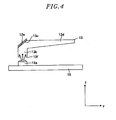
- Fig. 4 is a section view taken along line IV-IV in Fig. 3 , showing the light guide plate 13 in which the reflection sheet 13a is bonded to the outer surface thereof to cover the main reflection surface 13c.
- one of the LEDs 15a mounted to the substrate 15 is also shown in Fig. 4 .
- the LEDs 15a arranged and mounted on the substrate 15 emit light
- the light thus emitted is incident on the incident portion 13b of the light guide plate 13 through the frame 14 (not shown in Fig. 4 ) and the light incident surface 13f of the light guide plate 13.
- the light incident on the incident portion 13b of the light guide plate 13 is reflected by the main reflection surface 13c of the light guide plate 13, thus traveling toward the irradiation portion 13d of the light guide plate 13.
- the irradiation portion 13d of the light guide plate 13 makes the light uniform and illuminates the liquid crystal panel 12 from the rear side thereof.
- the light incident on the main reflection surface 13c is not fully reflected but may partially transmit the main reflection surface 13c.
- the reflection sheet 13a is bonded to the outer surface of the light guide plate 13 so that it can cover the main reflection surface 13c of the light guide plate 13 to reflect the light penetrating the main reflection surface 13c.
- the reflection sheet 13a is made of a highly reflective material. Use of the reflection sheet 13a improves the reflectivity of the main reflection surface 13c of the light guide plate 13.
- the light emitted from the LEDs 15a as a light source is well irradiated on the liquid crystal panel 12, consequently enhancing the backlight brightness in the backlight unit 10.
- the reflection sheet 13a as an auxiliary reflection surface makes it possible to orient the light source so that the axis of the light source can extend in the thickness direction of the substrate 15. Therefore, it is possible to arrange the light source between the light guide plate 13 and the substrate 15. In other words, there is no need to provide a space near the end surface of the light guide plate 13 as in the case where the light source is arranged on the end surface of the light guide plate 13. Accordingly, it is possible to reduce the size of the light guide plate 13 as compared with the case where the light source is arranged on the end surface of the light guide plate 13.
- a reflection member 13e for reflecting the light which comes from the light incident surface 13f of the light guide plate 13 and passes through the main reflection surface 13c, toward the main reflection surface 13c may be attached to the outer surface of the light guide plate 13 so that it can cover the main reflection surface 13c of the light guide plate 13.
- the reflection member 13e include a bonding structure of a resin-made or metal-made sheet, a vapor deposition structure of a metal foil and a structure in which a separate member is brought into close contact with the outer surface of the main reflection surface 13c.
- Fig. 5 is a perspective view showing the light guide plate 13, to which the reflection member 13e is attached to cover the main reflection surface 13c of the light guide plate 13, and the liquid crystal panel 12.
- Fig. 6 is a section view taken along line VI-VI in Fig. 5 , showing the light guide plate 13 to which the reflection member 13e is attached to cover the main reflection surface 13c of the light guide plate 13.
- one of the LEDs 15a arranged and mounted on the substrate 15 is illustrated in Fig. 6 .
- the LEDs 15a arranged and mounted on the substrate 15 emit light
- the light thus emitted is incident on the incident portion 13b of the light guide plate 13 through the frame 14 (not shown in Fig. 6 ) and the light incident surface 13f of the light guide plate 13.
- the light incident on the incident portion 13b of the light guide plate 13 is reflected by the main reflection surface 13c of the light guide plate 13, thus traveling toward the irradiation portion 13d of the light guide plate 13.
- the irradiation portion 13d of the light guide plate 13 makes the light uniform and illuminates the liquid crystal panel 12 from the rear side thereof.
- the light incident on the main reflection surface 13c is not fully reflected but may partially transmit the main reflection surface 13c.
- the reflection member 13e is attached to the outer surface of the light guide plate 13 so that it can cover the main reflection surface 13c of the light guide plate 13 to reflect the light penetrating the main reflection surface 13c.
- the reflection member 13e is made of a highly reflective material. Use of the reflection member 13e improves the reflectivity of the main reflection surface 13c of the light guide plate 13. Thus, the light emitted from the LEDs 15a is well irradiated on the liquid crystal panel 12, consequently enhancing the backlight brightness in the backlight unit 10.
- the reflection member 13e as an auxiliary reflection surface makes it possible to provide the reflection member 13e outside the main reflection surface 13c. Therefore, the light penetrating the main reflection surface 13c is reflected into the light guide plate 13 by the reflection member 13e. Accordingly, the light emitted from the light source is reliably launched from the launching surface of the light guide plate 13 through the main reflection surface 13c. This helps prevent occurrence of brightness reduction.
- a covering portion 14a for covering the main reflection surface 13c may be provided in the frame 14 as illustrated in Fig. 7 .
- the covering portion 14a may include a reflection portion 14a1 (see Fig. 8 ) that serves as a covering surface for reflecting the light toward the main reflection surface 13c.
- the reflection portion 14a1 makes up a reflection layer in the covering portion 14a of the frame 14.
- Fig. 8 is a section view of the frame 14 taken along line VIII-VIII in Fig. 7 . In this regard, it does not matter whether the covering surface is in contact with the outer surface of the main reflection surface 13c.
- Examples of the reflection layer of the frame 14 include a bonding structure of a resin-made or metal-made sheet, a vapor deposition structure of a metal foil, a structure in which a separate member is brought into close contact with the outer surface of the main reflection surface 13c, and a frame structure formed of a material with desired surface reflectivity.
- the reflection portion 14a1 of the covering portion 14a of the frame 14 provides a frame reflection layer on the covering surface. Therefore, the light penetrating the main reflection surface 13c is reflected into the light guide plate 13 by the frame reflection layer. Accordingly, the light emitted from the light source is reliably launched from the launching surface of the light guide plate 13 through the main reflection surface 13c. This helps prevent occurrence of brightness reduction.
- the frame 14 may include a fixing portion 14b for fixing the liquid crystal panel 12 in place.
- Fig. 9 is a perspective view showing the frame 14 provided with the fixing portion 14b for fixing the liquid crystal panel 12 in place. A part of the liquid crystal panel 12 is illustrated by a dot line in Fig. 9 .
- the liquid crystal panel 12 is fixed in place by the covering portion 14a and the fixing portion 14b of the frame 14.
- the frame 14 plays a role of supporting and fixing the liquid crystal panel 12. There is no need to provide other members than the frame 14 to fix the liquid crystal panel 12. This provides an advantageous effect in that it is possible to reduce the number of parts required in manufacturing the display device 1 of the first embodiment, thereby further reducing the component parts of the display device 1.
- the frame 14 may include a surrounding member 14c arranged between the substrate 15 and the frame 14.
- the surrounding member 14c has transmission holes for passing the light emitted from the light source and surrounds the light source.
- the surrounding member 14c is made of a material having reflectivity substantially equal to or greater than that of the substrate 15.
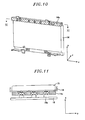
- Fig. 10 is a rear perspective view showing the surrounding member 14c attached between the substrate 15 and the frame 14 to surround the LEDs 15a as a light source.
- Fig. 11 is a section view taken along line XI-XI in Fig. 10 , showing the relationship between the surrounding member 14c for reflecting the light emitted from the LEDs 15a, the frame 14, the LEDs 15a arranged and mounted on the substrate 15 and the light guide plate 13.
- the LEDs 15a arranged and mounted on the substrate 15 is covered by the surrounding member 14c, the light emitted from the light source in other directions than the light incident surface is reflected toward the light incident surface by the surrounding member 14c or the surrounding portion. This makes it possible to realize high brightness.
- the light guide plate 13, the frame 14 and the substrate 15 are actually kept in close contact with each other, although they are separated from each other in the drawings.
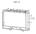
- the frame 14 may be made of a material having reflectivity substantially equal to or greater than that of the substrate 15 and may include surrounding portions 14d for surrounding the light source as shown in Fig. 12 , each of the surrounding portions 14d having a transmission hole for passing the light emitted from the LEDs 15a.
- Fig. 13 is a section view of the frame 14 taken along the z-x plane in Fig. 12 .
- the surrounding portions 14d of the frame 14 provides a substrate reflection layer around the light source in the substrate 15, the light emitted toward the substrate 15 is reflected by the substrate reflection layer to go toward the light incident surface. This makes it possible to realize high brightness.
- a substrate reflection layer for reflecting the lights emitted from the LEDs 15a may be provided around the LEDs 15a arranged and mounted on the substrate 15.
- Fig. 14 is a perspective view showing the substrate 15, in which reflection devisal is applied around the LEDs 15a, and the frame 14.
- Examples of the method for forming the substrate reflection layer include applying white silk to the area around the LEDs 15a, applying white resist to the area around the LEDs 15a, bonding a dedicated reflective sheet to the area around the LEDs 15a and providing a dedicated reflective member. This makes it possible to efficiently reflect the light emitted from the LEDs 15a, thereby enhancing the backlight brightness.
- Fig. 15 is a section view showing one example of the combination of the liquid crystal panel 12, the light guide plate 13, the frame 14 and the substrate 15. Only one of the LEDs 15a is representatively illustrated in Fig. 15 . With this configuration, it is possible to save the material of the light guide plate 13, thereby shortening the distance between the light guide plate 13 and the substrate 15 and reducing the thickness of the display device 1.
- the lights emitted from the LEDs 15a may be incident on the light incident surface 13f of the light guide plate 13 along the direction (toward the y-direction negative side).
- the LEDs 15a are oriented so that the optical axes thereof can extend in the direction parallel to the plane of the substrate 15.
- Fig. 16 is a section view showing another example of the combination of the liquid crystal panel 12, the light guide plate 13, the frame 14 and the substrate 15. Only one of the LEDs 15a is representatively illustrated in Fig. 16 . Since the light source is oriented so that the optical axis thereof can extend in the direction parallel to the plane of the substrate 15, there is no need to form the light guide plate 13 into an I-like shape or an L-like shape. Furthermore, the light can be guided by the light guide plate 13 even if the LEDs 15a emit the light in the direction parallel to the plane of the substrate 15.
- the LEDs as a light source are not limited to LEDs emitting single color light (e.g., red light). Two or three kinds of LEDs selected from red LEDs, green LEDs and blue LEDs may be alternately arranged. No particular restriction is imposed on the number of LEDs as a light source, the kind of emitted light colors and the number of emitted light colors.
Landscapes
- Physics & Mathematics (AREA)
- General Physics & Mathematics (AREA)
- Optics & Photonics (AREA)
- Liquid Crystal (AREA)
- Planar Illumination Modules (AREA)
Applications Claiming Priority (1)
| Application Number | Priority Date | Filing Date | Title |
|---|---|---|---|
| JP2009267986A JP4931985B2 (ja) | 2009-11-25 | 2009-11-25 | バックライトユニット及びこれを用いた表示器 |
Publications (1)
| Publication Number | Publication Date |
|---|---|
| EP2333592A2 true EP2333592A2 (de) | 2011-06-15 |
Family
ID=43530282
Family Applications (1)
| Application Number | Title | Priority Date | Filing Date |
|---|---|---|---|
| EP10014623A Withdrawn EP2333592A2 (de) | 2009-11-25 | 2010-11-15 | Rückbeleuchtungseinheit und Anzeigevorrichtung damit |
Country Status (5)
| Country | Link |
|---|---|
| US (1) | US20110122650A1 (de) |
| EP (1) | EP2333592A2 (de) |
| JP (1) | JP4931985B2 (de) |
| CN (1) | CN102141219A (de) |
| TW (1) | TWI436132B (de) |
Families Citing this family (8)
| Publication number | Priority date | Publication date | Assignee | Title |
|---|---|---|---|---|
| JP5829845B2 (ja) * | 2011-07-01 | 2015-12-09 | パナソニック デバイスSunx株式会社 | 表示器 |
| US8558971B2 (en) * | 2011-09-14 | 2013-10-15 | Shenzhen China Star Optoelectronics Technology Co., Ltd. | Integrated liquid crystal display device |
| JP5906050B2 (ja) * | 2011-09-30 | 2016-04-20 | 株式会社小糸製作所 | 車両用灯具 |
| JP6212706B2 (ja) * | 2012-08-31 | 2017-10-18 | パナソニックIpマネジメント株式会社 | 表示装置 |
| JP2014116104A (ja) * | 2012-12-06 | 2014-06-26 | Panasonic Corp | 照明装置 |
| KR102409209B1 (ko) * | 2015-10-01 | 2022-06-16 | 삼성디스플레이 주식회사 | 표시 장치 |
| JP7121298B2 (ja) | 2019-12-27 | 2022-08-18 | 日亜化学工業株式会社 | 線状光源の製造方法 |
| TWI857525B (zh) * | 2023-03-15 | 2024-10-01 | 致伸科技股份有限公司 | 導光模組 |
Citations (1)
| Publication number | Priority date | Publication date | Assignee | Title |
|---|---|---|---|---|
| JP2004325959A (ja) | 2003-04-25 | 2004-11-18 | Matsushita Electric Works Ltd | 液晶バックライト装置 |
Family Cites Families (9)
| Publication number | Priority date | Publication date | Assignee | Title |
|---|---|---|---|---|
| JPH09160032A (ja) * | 1995-12-12 | 1997-06-20 | Omron Corp | 照明装置、並びに当該照明装置を用いた液晶表示装置、携帯端末機器、車載用機器及び光学的認識装置 |
| JP2000235183A (ja) * | 1999-02-16 | 2000-08-29 | Matsushita Electric Ind Co Ltd | 照明装置およびこれを備えた携帯情報機器 |
| JP2003109421A (ja) * | 2001-07-25 | 2003-04-11 | Toshiba Lighting & Technology Corp | バックライトユニットおよび表示装置 |
| JP2003092020A (ja) * | 2001-09-17 | 2003-03-28 | Seiko Instruments Inc | バックライト付き表示装置 |
| JP2003279971A (ja) * | 2002-03-20 | 2003-10-02 | Kawaguchiko Seimitsu Co Ltd | 液晶表示装置 |
| JP2004031180A (ja) * | 2002-06-27 | 2004-01-29 | Kawaguchiko Seimitsu Co Ltd | バックライト装置 |
| DE20210707U1 (de) * | 2002-07-11 | 2003-11-20 | Diehl AKO Stiftung & Co. KG, 88239 Wangen | Hinterleuchtete Flüssigkristallanzeige, insbesondere zum Einsatz als Anzeigemodul hinter der Bedienblende eines Haushaltsgroßgerätes |
| JP2004117435A (ja) * | 2002-09-24 | 2004-04-15 | Kawaguchiko Seimitsu Co Ltd | 液晶表示パネルのバックライト構造 |
| JP2004119031A (ja) * | 2002-09-24 | 2004-04-15 | Kawaguchiko Seimitsu Co Ltd | 液晶表示パネルのバックライト装置 |
-
2009
- 2009-11-25 JP JP2009267986A patent/JP4931985B2/ja active Active
-
2010
- 2010-11-15 EP EP10014623A patent/EP2333592A2/de not_active Withdrawn
- 2010-11-24 CN CN2010105691012A patent/CN102141219A/zh active Pending
- 2010-11-24 US US12/926,534 patent/US20110122650A1/en not_active Abandoned
- 2010-11-25 TW TW099140804A patent/TWI436132B/zh active
Patent Citations (1)
| Publication number | Priority date | Publication date | Assignee | Title |
|---|---|---|---|---|
| JP2004325959A (ja) | 2003-04-25 | 2004-11-18 | Matsushita Electric Works Ltd | 液晶バックライト装置 |
Also Published As
| Publication number | Publication date |
|---|---|
| US20110122650A1 (en) | 2011-05-26 |
| JP4931985B2 (ja) | 2012-05-16 |
| TW201128269A (en) | 2011-08-16 |
| CN102141219A (zh) | 2011-08-03 |
| TWI436132B (zh) | 2014-05-01 |
| JP2011113752A (ja) | 2011-06-09 |
Similar Documents
| Publication | Publication Date | Title |
|---|---|---|
| EP2333592A2 (de) | Rückbeleuchtungseinheit und Anzeigevorrichtung damit | |
| CN101896765B (zh) | 照明装置和液晶显示装置 | |
| EP2192438B1 (de) | Flüssigkristallanzeigevorrichtung | |
| CN112764264B (zh) | 直下式背光装置和具有该背光装置的显示设备 | |
| EP3726285B1 (de) | Elektronische vorrichtung und anzeigeanordnung und rückbeleuchtungsmodul dafür | |
| CN205619047U (zh) | 照明装置、显示装置及电视接收装置 | |
| US20190121199A1 (en) | Backlight module and display device | |
| JP2006286638A (ja) | 複数の隣り合って重なり合う導光板を有する発光装置 | |
| CN111665661B (zh) | 背光装置以及液晶显示装置 | |
| KR20100067482A (ko) | 광출사 모듈 및 이를 갖는 표시장치 | |
| WO2011070724A1 (ja) | 照明装置及びそれを備えた液晶表示装置 | |
| TWI576880B (zh) | 背光模組及使用其之鍵盤 | |
| WO2011093119A1 (ja) | 照明装置、表示装置、テレビ受信装置 | |
| JP2019125519A (ja) | 照明装置および表示装置 | |
| KR101453954B1 (ko) | 백라이트 유닛 및 이를 포함하는 액정 표시 장치 | |
| CN102197256A (zh) | 照明装置、面光源装置、显示装置和电视接收装置 | |
| US8579491B2 (en) | Backlight unit and display apparatus having the same | |
| US8950926B2 (en) | Planar light source apparatus and display apparatus using the same | |
| KR20070112312A (ko) | 백라이트 어셈블리 및 이를 갖는 표시 장치 | |
| CN103732973A (zh) | 照明装置和具备它的显示装置 | |
| WO2012066887A1 (ja) | 照明装置およびこれを備えた液晶表示装置 | |
| WO2012050052A1 (ja) | バックライトユニットおよび液晶表示装置 | |
| JP2010123345A (ja) | 面状照明装置および液晶表示装置 | |
| JP2013182854A (ja) | 照明装置及びそれを備えた表示装置 | |
| JP2010276628A (ja) | 液晶表示装置 |
Legal Events
| Date | Code | Title | Description |
|---|---|---|---|
| PUAI | Public reference made under article 153(3) epc to a published international application that has entered the european phase |
Free format text: ORIGINAL CODE: 0009012 |
|
| AK | Designated contracting states |
Kind code of ref document: A2 Designated state(s): AL AT BE BG CH CY CZ DE DK EE ES FI FR GB GR HR HU IE IS IT LI LT LU LV MC MK MT NL NO PL PT RO RS SE SI SK SM TR |
|
| AX | Request for extension of the european patent |
Extension state: BA ME |
|
| STAA | Information on the status of an ep patent application or granted ep patent |
Free format text: STATUS: THE APPLICATION HAS BEEN WITHDRAWN |
|
| 18W | Application withdrawn |
Effective date: 20131007 |