EP2329477B1 - Composant optoélectronique - Google Patents
Composant optoélectronique Download PDFInfo
- Publication number
- EP2329477B1 EP2329477B1 EP09736802.1A EP09736802A EP2329477B1 EP 2329477 B1 EP2329477 B1 EP 2329477B1 EP 09736802 A EP09736802 A EP 09736802A EP 2329477 B1 EP2329477 B1 EP 2329477B1
- Authority
- EP
- European Patent Office
- Prior art keywords
- diode chip
- optoelectronic device
- luminescence diode
- shield
- shielding region
- Prior art date
- Legal status (The legal status is an assumption and is not a legal conclusion. Google has not performed a legal analysis and makes no representation as to the accuracy of the status listed.)
- Active
Links
- 230000005693 optoelectronics Effects 0.000 title claims description 142
- 238000004020 luminiscence type Methods 0.000 claims description 82
- 230000005855 radiation Effects 0.000 claims description 44
- 230000005670 electromagnetic radiation Effects 0.000 claims description 21
- 239000006096 absorbing agent Substances 0.000 claims description 19
- 238000004382 potting Methods 0.000 claims description 17
- 238000010521 absorption reaction Methods 0.000 claims description 7
- 230000002745 absorbent Effects 0.000 claims description 6
- 239000002250 absorbent Substances 0.000 claims description 6
- 239000004020 conductor Substances 0.000 claims description 3
- 239000000463 material Substances 0.000 description 8
- 230000003287 optical effect Effects 0.000 description 7
- 238000005538 encapsulation Methods 0.000 description 5
- 238000001746 injection moulding Methods 0.000 description 4
- 238000001721 transfer moulding Methods 0.000 description 4
- 230000015572 biosynthetic process Effects 0.000 description 3
- 239000011521 glass Substances 0.000 description 3
- 238000002310 reflectometry Methods 0.000 description 3
- 239000011248 coating agent Substances 0.000 description 2
- 238000000576 coating method Methods 0.000 description 2
- 239000002184 metal Substances 0.000 description 2
- 238000000034 method Methods 0.000 description 2
- 239000007787 solid Substances 0.000 description 2
- XLYOFNOQVPJJNP-UHFFFAOYSA-N water Substances O XLYOFNOQVPJJNP-UHFFFAOYSA-N 0.000 description 2
- 238000005452 bending Methods 0.000 description 1
- 239000006229 carbon black Substances 0.000 description 1
- 239000000969 carrier Substances 0.000 description 1
- 238000005266 casting Methods 0.000 description 1
- 229910010293 ceramic material Inorganic materials 0.000 description 1
- 235000013351 cheese Nutrition 0.000 description 1
- 239000003086 colorant Substances 0.000 description 1
- 238000004040 coloring Methods 0.000 description 1
- 230000007423 decrease Effects 0.000 description 1
- 230000008021 deposition Effects 0.000 description 1
- 230000007613 environmental effect Effects 0.000 description 1
- 238000005530 etching Methods 0.000 description 1
- 238000002347 injection Methods 0.000 description 1
- 239000007924 injection Substances 0.000 description 1
- 238000000059 patterning Methods 0.000 description 1
- 229920001296 polysiloxane Polymers 0.000 description 1
- 239000004071 soot Substances 0.000 description 1
- 230000003595 spectral effect Effects 0.000 description 1
- 230000000007 visual effect Effects 0.000 description 1
Images

Classifications
-
- H—ELECTRICITY
- H01—ELECTRIC ELEMENTS
- H01L—SEMICONDUCTOR DEVICES NOT COVERED BY CLASS H10
- H01L33/00—Semiconductor devices with at least one potential-jump barrier or surface barrier specially adapted for light emission; Processes or apparatus specially adapted for the manufacture or treatment thereof or of parts thereof; Details thereof
- H01L33/48—Semiconductor devices with at least one potential-jump barrier or surface barrier specially adapted for light emission; Processes or apparatus specially adapted for the manufacture or treatment thereof or of parts thereof; Details thereof characterised by the semiconductor body packages
- H01L33/58—Optical field-shaping elements
- H01L33/60—Reflective elements
-
- G—PHYSICS
- G09—EDUCATION; CRYPTOGRAPHY; DISPLAY; ADVERTISING; SEALS
- G09F—DISPLAYING; ADVERTISING; SIGNS; LABELS OR NAME-PLATES; SEALS
- G09F27/00—Combined visual and audible advertising or displaying, e.g. for public address
- G09F27/008—Sun shades, shades, hoods or louvres on electronic displays to minimise the effect of direct sun light on the display
-
- H—ELECTRICITY
- H01—ELECTRIC ELEMENTS
- H01L—SEMICONDUCTOR DEVICES NOT COVERED BY CLASS H10
- H01L2224/00—Indexing scheme for arrangements for connecting or disconnecting semiconductor or solid-state bodies and methods related thereto as covered by H01L24/00
- H01L2224/01—Means for bonding being attached to, or being formed on, the surface to be connected, e.g. chip-to-package, die-attach, "first-level" interconnects; Manufacturing methods related thereto
- H01L2224/42—Wire connectors; Manufacturing methods related thereto
- H01L2224/47—Structure, shape, material or disposition of the wire connectors after the connecting process
- H01L2224/48—Structure, shape, material or disposition of the wire connectors after the connecting process of an individual wire connector
- H01L2224/4805—Shape
- H01L2224/4809—Loop shape
- H01L2224/48091—Arched
-
- H—ELECTRICITY
- H01—ELECTRIC ELEMENTS
- H01L—SEMICONDUCTOR DEVICES NOT COVERED BY CLASS H10
- H01L2224/00—Indexing scheme for arrangements for connecting or disconnecting semiconductor or solid-state bodies and methods related thereto as covered by H01L24/00
- H01L2224/01—Means for bonding being attached to, or being formed on, the surface to be connected, e.g. chip-to-package, die-attach, "first-level" interconnects; Manufacturing methods related thereto
- H01L2224/42—Wire connectors; Manufacturing methods related thereto
- H01L2224/47—Structure, shape, material or disposition of the wire connectors after the connecting process
- H01L2224/48—Structure, shape, material or disposition of the wire connectors after the connecting process of an individual wire connector
- H01L2224/481—Disposition
- H01L2224/48151—Connecting between a semiconductor or solid-state body and an item not being a semiconductor or solid-state body, e.g. chip-to-substrate, chip-to-passive
- H01L2224/48221—Connecting between a semiconductor or solid-state body and an item not being a semiconductor or solid-state body, e.g. chip-to-substrate, chip-to-passive the body and the item being stacked
- H01L2224/48245—Connecting between a semiconductor or solid-state body and an item not being a semiconductor or solid-state body, e.g. chip-to-substrate, chip-to-passive the body and the item being stacked the item being metallic
- H01L2224/48247—Connecting between a semiconductor or solid-state body and an item not being a semiconductor or solid-state body, e.g. chip-to-substrate, chip-to-passive the body and the item being stacked the item being metallic connecting the wire to a bond pad of the item
-
- H—ELECTRICITY
- H01—ELECTRIC ELEMENTS
- H01L—SEMICONDUCTOR DEVICES NOT COVERED BY CLASS H10
- H01L33/00—Semiconductor devices with at least one potential-jump barrier or surface barrier specially adapted for light emission; Processes or apparatus specially adapted for the manufacture or treatment thereof or of parts thereof; Details thereof
- H01L33/48—Semiconductor devices with at least one potential-jump barrier or surface barrier specially adapted for light emission; Processes or apparatus specially adapted for the manufacture or treatment thereof or of parts thereof; Details thereof characterised by the semiconductor body packages
- H01L33/58—Optical field-shaping elements
Definitions
- An optoelectronic component is specified.
- An object to be solved is to provide an optoelectronic component which is particularly well protected against environmental influences such as extraneous light and / or rainwater. Another object to be solved is to provide an optoelectronic component which can be mounted particularly easily.
- the component comprises at least one luminescence diode chip.
- the luminescence diode chip is preferably a laser diode chip or a light-emitting diode chip.
- the luminescence diode chip is suitable for generating electromagnetic radiation.
- the electromagnetic radiation may be in the wavelength range from UV radiation to infrared light.
- the luminescence diode chip is suitable for generating electromagnetic radiation in the visible spectral range.
- the component comprises at least one shield against external radiation.
- External radiation is from the outside, ie from outside the optoelectronic component, to Radiation incident on the component.
- it is sunlight or the light of bulbs such as headlights.
- the extraneous radiation if it is not shielded, can hit the luminescence diode chip or another component of the optoelectronic component, such as a lens, for example, and be reflected there.
- electromagnetic radiation emitted by the optoelectronic component during operation is distorted.
- the unwanted electromagnetic radiation is also referred to as phantom radiation.
- the shield is now suitable for preventing the extraneous radiation from the luminescence diode chip and / or other components of the optoelectronic component.
- the shield surrounds the luminescence diode chip only in places laterally. That is, the shield is laterally adjacent, preferably laterally spaced from the LED chip, the shield not completely surrounding the LED chip laterally, but the shield only surrounds the LED chip at selected locations, such as along a single side surface.
- the shield is arranged such that it can shield extraneous radiation from an external radiation source from the luminescence diode chip and / or further optical components of the optoelectronic component. If the shield is provided, for example, as a shield against sunlight, then the shield surrounds the luminescence diode chip, preferably on sides of the luminescence diode chip, which face the sun. The shield casts a shadow in which the be shielded components at least partially or completely.
- the shield is formed integrally with at least one component of the optoelectronic component. That is, the shield is formed as one piece with another component of the optoelectronic device.
- the shield forms part or a portion of the component.
- “Integral” may also mean in particular that no interface between the shield and the component is arranged.
- the shield and the component may be made together, for example.
- the shield is also possible for the shield to be integrally formed with a plurality of components of the optoelectronic component.
- the optoelectronic component in this case comprises a plurality of shields, wherein each shield is formed integrally with a component of the optoelectronic component. That is, the optoelectronic component may comprise one, two or more shields, wherein each shield is formed integrally with another component of the optoelectronic device.
- the component comprises at least one luminescence diode chip which emits electromagnetic radiation during operation of the optoelectronic component. Furthermore, the optoelectronic component comprises at least one shield against extraneous radiation, which surrounds the luminescence diode chip only in places laterally. Each of the shields is integral with a component the optoelectronic component is formed.
- the components may be, for example, connection carriers, printed circuit boards, optical elements such as lenses, housing bases, and / or reflector walls.
- the optoelectronic component described here is based on the knowledge that a shield, which is integrally formed with a component of the component, reduces the assembly effort of the optoelectronic component. So it is no longer necessary to adjust the optoelectronic component and shield separately. Further, the integral formation of the shield with a component of the optoelectronic device increases the mechanical stability of the optoelectronic device, since a separately attached to the optoelectronic device or in the vicinity of the optoelectronic device shield can be separated from the optoelectronic device, for example, due to external weather conditions easier than one piece with formed a component of the component shield.
- the optoelectronic component comprises a connection carrier.
- the connection carrier is a printed circuit board which has electrical connection points for the electrical connection of the at least one luminescence diode chip.
- the printed circuit board on conductor tracks, by means of which the at least one Lumineszenzdiodenchip can be electrically contacted.
- the printed circuit board may, for example, comprise an electrically insulating main body into which or onto which the electrical connection points and the conductor tracks are structured.
- connection carrier is a carrier frame (lead frame, also leadframe).
- a support frame also serves for attachment and electrical contacting of the at least one LED chip.
- the at least one luminescence diode chip is attached at least indirectly to the connection carrier.
- the luminescence diode chip can be applied directly to the connection carrier. Moreover, it is possible for further components to be present between the luminescence diode chip and the connection carrier.
- the at least one luminescence diode chip is electrically contacted via the connection carrier. That is, by means of the connection carrier, the at least one luminescence diode chip can be energized during operation of the optoelectronic component.
- the at least one shield is formed at least in places by a shielding region of the connection carrier.
- the shield is thus integral with the connection carrier, and thus formed with a component of the optoelectronic component.
- connection carrier has at least two partial regions: a shielding region which forms at least one shielding of the optoelectronic component against external radiation.
- the shielding area is such arranged that it surrounds the LED chip only in places laterally.
- the shielding region of the connection carrier is, for example, free of a luminescence diode chip.
- connection carrier comprises a remaining region on which, for example, the at least one luminescence diode chip is arranged.
- the component comprises a connection carrier on which the at least one luminescence diode chip is at least indirectly fixed and via which the at least one luminescence diode chip is electrically contacted.
- at least one shielding of the optoelectronic component is formed by a shielding region of the connection carrier.
- connection carrier has a bend. This bend connects the shielding area of the connection carrier with the remaining connection carrier, on which, for example, the at least one luminescence diode chip is at least indirectly fixed.
- the connection carrier is preferably made of a bendable material.
- connection carrier has a bend, so that the shielding region is arranged at a certain angle to the connection carrier.
- the shielding region and the remaining connection carrier are arranged at an angle of less than or equal to 110 ° to one another.
- the shielding area and the rest of the connection carrier form an angle of less than or equal to 110 ° with each other.
- the connection carrier is designed to be bendable in such a way that the user of the optoelectronic component, for example after the assembly of the optoelectronic component, can adjust the angle between the shielding area and the remaining connection carrier in a specific area. In this way it is possible to optimally adapt the shielding to the place of use of the optoelectronic component.
- the component comprises a reflector wall which completely surrounds the at least one luminescence diode chip laterally.
- the reflector wall is suitable for the reflection of electromagnetic radiation generated by the luminescence diode chip during operation.
- the reflector wall preferably has a reflectivity for the electromagnetic radiation generated by the luminescence diode chip during operation of at least 90%, preferably of at least 95%:
- the reflector wall may be formed from a white ceramic material or with a metal.
- the reflector wall surrounds the at least one luminescence diode chip laterally completely, that is, it is arranged like a frame around the luminescence diode chip.
- frame-like does not refer to the geometry of the reflector wall, but is intended only for Express expression that the LED chip is laterally completely enclosed by the reflector wall.
- the reflector wall has an uneven height. That is, the reflector wall has areas where it is higher than in other areas. For example, in one revolution around the at least one light-emitting diode chip, the height of the reflector wall initially increases, reaches a maximum height, decreases, until it reaches a minimum height.
- At least one shielding of the component against extraneous radiation is formed at least in places by a shielding region of the reflector wall.
- the shield is formed in one piece with the reflector wall, that is to say a component of the optoelectronic component, by means of the shielding region.
- the shielding of the reflector wall is formed higher than the rest of the reflector wall. That is, in one revolution around the at least one luminescence diode chip, the reflector wall has an area in which the height rises, reaches a maximum and falls to the initial value of the height.
- the shielding region is then formed by the region of the reflector wall in which the height increases, reaches a maximum and drops to the initial value.
- the component comprises a reflector wall which completely surrounds the at least one luminescence diode chip laterally, wherein the reflector wall has an uneven height.
- at least a shielding of the optoelectronic component against extraneous radiation is formed at least in places by a shielding region of the reflector wall, which is designed to be higher than the remaining reflector wall.
- the reflector wall is arranged within a lens for the at least one luminescence diode chip.
- the lens may span the reflector wall and the at least one luminescence diode chip in the manner of a dome.
- the reflector wall and the luminescence diode chip can then adjoin a gas, for example air.
- the lens is formed as a solid body, which is applied in the manner of a potting on the LED chip and the reflector wall.
- reflector wall and the at least one LED chip are embedded in the material of the lens, so a casting. It is also possible that the potting is not formed lens-like, but has flat side surfaces and a flat top surface. In any case, the reflector wall in this embodiment at least in places directly adjoins a potting for the at least one luminescence diode chip.
- the reflector wall and thus the shield which is formed by a shielding region of the reflector wall, are particularly well protected by the potting from external influences.
- the shielding area is thus protected against external weather influences as well as against mechanical stress.
- the shield does not provide protection against external radiation for the entire potting.
- the potting itself must therefore be particularly resistant to external radiation, for example, protected against UV radiation, and against external influences such as rainwater in this case.
- the optoelectronic component can comprise a further shield, which is formed by the shielding region of a connection carrier.
- particularly UV-resistant materials such as silicone, find use.
- the component instead of the reflector wall, the component has an absorber wall which absorbs electromagnetic radiation impinging on it. Otherwise, the absorber wall is formed like the described reflector wall.
- the absorber wall is black, for example. It can - for example, with a color - be coated black, or from a black material - such as soot-filled plastic - be formed.
- the absorber wall suppresses, for example, the formation of stray radiation.
- the absorber wall has a reflectivity of preferably less than 10%, particularly preferably less than 5%, for light striking it.
- the reflector wall or the absorber wall is formed integrally with a carrier of the component.
- the reflector wall or the absorber wall and the carrier are produced by a common injection molding process or a common transfer molding process. That is, the reflector wall or the absorber wall and the carrier are injection molded or injection-molded together. It is an objective feature that can be detected on the finished component.
- the optoelectronic component comprises a housing base body.
- the housing base is made of a plastic material, for example.
- the housing base body can have a cavity in which the at least one luminescence diode chip is arranged.
- the luminescence diode chip is then laterally surrounded in the cavity by a housing wall of the housing base body, which may be formed as a reflector wall.
- This reflector wall has a uniform height.
- the reflector wall as described above has a non-uniform height and thereby forms one of the shielding of the optoelectronic device against extraneous radiation.
- At least one shielding of the component is formed at least in places by a shielding region of the housing base body. That is, integral with the housing body and thus integral with a component of the optoelectronic component, a shielding region of the housing base body is formed, in which the housing base body is designed, for example, in the manner of a projection. This projection surrounds the luminescence diode chip laterally only in places.
- the component comprises a housing base body which has a cavity in which the at least one luminescence diode chip is arranged.
- at least one shielding of the optoelectronic component against external radiation is formed at least in places by a shielding region of the housing base body.
- the shielding region of the housing base body can be arranged inside or outside a lens and / or an encapsulation for the at least one luminescence diode chip.
- the shielding region can be produced in a particularly simple manner together with the housing base body, for example by means of transfer molding or injection molding. That is, according to at least one embodiment of the optoelectronic component described here, the shielding area is injection-molded or injection-molded together with the rest of the housing main body. In the case of "injection-molded" or "injection-molded”, these are objective features that can be detected on the finished product. That is, it can be demonstrated on the finished product that the shielding area was designed in one piece with the housing base body by injection molding or transfer molding.
- the housing base body can for example be poured or sprayed in places around a connection carrier, on which the at least one luminescence diode chip is attached at least indirectly.
- the optoelectronic component comprises a lens for the at least one luminescence diode chip.
- the lens is an optical element which, for example, increases the probability of decoupling electromagnetic radiation from the optoelectronic component.
- the lens may have jet-forming properties.
- the lens may be focusing or scattering for the passing electromagnetic radiation.
- At least one shielding of the optoelectronic component against extraneous radiation is formed at least in places by a shielding region of the lens. That is, the lens includes at certain locations a shielding area formed by patterning, coating, or partially coloring the lens.
- the lens in the shielding region can be polarizing, absorbing and / or reflecting. This can be realized, for example, by a partial coating of the outer surface of the lens facing away from the at least one luminescence diode chip with a metal.
- the component comprises a lens for the at least one luminescence diode chip, wherein at least one shield of the optoelectronic component is formed by a shielding region of the lens.
- At least one of the shields of the optoelectronic component has at least one reflection region, which faces the at least one luminescence diode chip and is designed to be reflective for electromagnetic radiation generated by the luminescence diode chip during operation of the optoelectronic component.
- radiation generated by the luminescence diode chip can partially strike the reflection region of the shield during operation of the optoelectronic component and is reflected there.
- the reflectance is preferably at least 90%, more preferably at least 95%.
- the remaining areas of the shielding are preferably designed to absorb radiation. That is, they absorb the incident extraneous radiation, so that no scattered light arises on the shield, which could disturb the visual impression of the optoelectronic component.
- the shield is formed radiopaque for the extraneous radiation, so that no extraneous radiation can pass through the shield on to be shielded areas of the optoelectronic device.
- the shield is at least in an absorption region, which faces the at least one LED chip for, from Luminescence diode chip formed in the operation of the optoelectronic component generated electromagnetic radiation absorbing. That is, no reflection or hardly any reflection of the incident electromagnetic radiation of the luminescence diode chip takes place in these absorption regions, but this radiation is absorbed in the absorption region.
- the degree of absorption is preferably at least 90, more preferably at least 95%.
- the shield may be designed to be reflective or absorbing in the entire area facing the at least one luminescence diode chip.
- the shield may have reflecting regions formed thereon and absorbent absorption regions formed in a reflective manner.
- At least one of the shields has a curvature.
- “Curvature” means that the shield in the manner of an arc, a spherical segment, a spherical shell segment, a hollow cylinder segment or similar geometric figures in places laterally led around the at least one LED chip.
- Such a design of the shield can prove to be advantageous in two ways.
- such a shield if it is designed to be absorbent and / or reflective in its region facing the luminescence diode chip, can perform optical tasks in the optoelectronic component. That is, the shield with curvature can contribute to the setting of a defined radiation characteristic of the optoelectronic device.
- the curvature may be suitable to pass moisture, in particular rainwater, which impinges from outside onto the optoelectronic component, around the radiation exit surface of the optoelectronic component.
- the radiation exit surface of the optoelectronic component is that optionally imaginary surface of the component through which the electromagnetic radiation generated during operation escapes to the outside.
- the radiation exit surface can be formed for example by the part of the outer surface of a lens or a potting.
- the curvature of the shield may be suitable for guiding rainwater around the radiation exit surface, in particular if the shield is formed outside a lens or encapsulation or integrally with a lens or encapsulation.
- the optoelectronic component described here can have exactly one of the shields described. Moreover, it is possible for the optoelectronic device described herein to have a combination of two or more of the shields described herein.
- the optoelectronic component can have a shield, which is formed by a shielding region of a connection carrier.
- the optoelectronic component can then have a shield, which is formed by the shielding region of a reflector wall.
- a lens for the at least one luminescence diode chip of the optoelectronic component can have a shielding region.
- the optoelectronic component described here is particularly suitable for forming a large-screen display, in which individual pixels are formed by an optoelectronic component described here. That is, the display is formed by a plurality of matrix-like arranged optoelectronic components. Each of the components in this case has at least one shield, which protects it from extraneous light, for example from sunlight.
- the shielding of each optoelectronic component can provide protection of the radiation exit surface of the component from rainwater. In this way, the display can also be operated under bad weather conditions. By diverting rainwater through a shield of the optoelectronic device does not lead to the deposition of water on the radiation exit surface of the component, so that scattered light due to water droplets, which act as unwanted optical elements, is suppressed.
- FIGS. 1A to 5B show examples and embodiments of optoelectronic components described here in schematic perspective views.
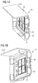
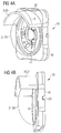
- the FIGS. 1A, 1B and 1C show a first example of an optoelectronic device described here with reference to schematic perspective views.
- the optoelectronic component 10 has four LED chips 1, which are formed as light emitting diode chips.
- the four LED chips 1 can emit light of the same color or different colors. For example, a luminescence diode chip 1 for generating blue light, a luminescence diode chip 1 for generating red light, and two luminescence diode chips 1 for generating green light are provided.
- the luminescence diode chips 1 are fastened on a connection carrier 20, which in the present case is designed as a metallic carrier frame.
- the luminescence diode chips 1 are surrounded by a potting 21.
- the outer surface of the encapsulation 21 facing away from the luminescence diode chips 1 forms the radiation exit surface 8 of the optoelectronic component 10.
- connection carrier 20 has tabs 25 in which it is bent up to the potting 21 out. This increases the adhesion of the potting 21 to the remaining components of the potting Optoelectronic device 10 such as the connection carrier 20 or the LED chips 1.
- the LED chips 1 may also be covered by a glass plate.
- the glass plate then preferably has on its side facing the luminescence diode chips 1 in the region of the luminescence diode chips 1 at least one recess in which it is reduced in thickness. In this recess, the LED chips 1 are arranged.
- the recess can be produced, for example, by etching the glass plate.
- the connection carrier 20 also has a shielding region 23, with which the connection carrier 20 is formed in one piece.
- the shielding region 23 is in principle an enlarged tab 25, which extends along a side surface of the optoelectronic component 10.
- the shielding region 23 projects beyond the potting 21 at least by the height of the potting 21.
- the shielding region 23 surrounds the luminescence diode chips 1 only in places laterally. That is, the shielding region 23 is arranged laterally adjacent to a side surface of the LED chip 1.
- the shielding region 23 does not completely surround the luminescence diode chips 1 laterally.
- the shielding region 23 forms the only shielding 3 of the optoelectronic component against extraneous radiation 4, which is incident on the component 10 from outside.
- the shielding region 23 is connected to the rest of the connection carrier 20 by means of a bend 24.
- the connection carrier 20 is bent in such a way that the shielding region 23 forms an angle ⁇ of approximately 90 ° with the remaining connection carrier 20.
- the inner surface of the shielding region 23 facing the luminescence diode chip 1 can be embodied as a reflection region 6 and / or as an absorption region 7. That is, depending on requirements, this surface is designed to be absorbent or reflective for electromagnetic radiation 2 generated by the LED chips 1 during operation.
- connection carrier 20 is formed so bendable that the user can optoelectronic component of the angle ⁇ by simple mechanical bending in a certain scope depending on the use of the optoelectronic device can be adjusted. This can be done easily to adapt the optoelectronic device to its place of use.
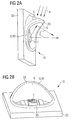
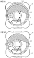
- FIGS. 2A and 2B show schematic perspective views of the optoelectronic component 10.
- the component 10 has a reflector wall 30.
- the reflector wall 30 has a non-uniform height. In its highest region-the shielding region 33 of the reflector wall-the reflector wall 30 forms the shield 3. That is, in this region the reflector wall shields extraneous radiation 4 from the optical components of the optoelectronic component.
- the reflector wall 30 is formed in the shielding region 33 on its side facing the luminescence diode chip 1 as a reflection region 6 which reflects radiation 2 generated by the luminescence diode chip 1 during operation.
- the reflector wall 30 may be applied to the carrier 32 as a separate component of the component.
- reflector wall 30 and support 32 are integrally formed with each other and are made for example by a common injection molding or a common transfer molding process with each other.
- the carrier 32 may be, for example, the electrically insulating basic body of the printed circuit board, via which the LED chip 1 is electrically contacted.
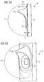
- the shielding region 33 is formed in one piece with the reflector wall 30 and is characterized in that it has a greater height H2 than the minimum height H1 of the reflector wall 30 (see also FIGS FIG. 3A ).
- the shielding 3, that is to say the shielding region 33 of the reflector wall, has a curvature 5 which, for example, dissipates rainwater, which can be incident from the same direction as the extraneous light 4, to the outside around the optical components of the optoelectronic component 10.
- the optoelectronic component 10 can also have an absorber wall 30 which absorbs electromagnetic radiation impinging on it.
- the absorber wall is black, for example. It can - for example with one color - be coated black, or from a black material - such as carbon black filled plastic - be formed.
- the absorber wall suppresses, for example, the formation of stray radiation.
- the absorber wall has a reflectivity of preferably less than 10%, particularly preferably less than 5%, for light striking it.
- the optoelectronic component 10 here has a lens 31 which surrounds both the luminescence diode chip 1 and the reflector wall 30 with shielding region 33.
- the lens 31 spans the components of the component 10 dome-like or dome-like.
- the lens 31 may be formed as a hollow body, so that it is slipped over the reflector wall 30 and Lumineszenzdiodenchip 1 in the manner of a cheese bell.
- the lens 31 is formed as a solid body.
- the lens 31 can be applied as a type of potting over the luminescence diode chip 1 and the reflector wall 30, so that the reflector wall 30 and thus the shielding region 33 are embedded in the encapsulation of the lens 31.
- the reflector wall 30 has a minimum height H1 in which it does not form a shielding region 33. Only in the region where the reflector wall 30 has a height greater than H1, with the maximum height H2, does it form the shielding region 33. That is, the shielding formed by the shielding region 33 surrounds the luminescence diode chip 1 only in places laterally. Because the reflector wall 30 has areas with a reduced height H1, the shield 3, that is to say the shielding area 33, is not completely around the shield Lumineszenzdiodenchip 1 led around. The reflector wall 30 is thus formed asymmetrically.
- the shielding 3 is here outside of the lens 31, 50 is arranged.
- the optoelectronic component 10 comprises a housing base body 40, which surrounds a connection carrier 20.
- the housing base body 40 is sprayed onto the connection carrier, which may be designed as a carrier strip.
- connection carrier 20 is overmolded with the material of the base body 40.
- the base body 40 has a cavity 41 in which the luminescence diode chip 1 is arranged.
- a reflector wall 30 Arranged around the luminescence diode chip 1 is a reflector wall 30, which in this case has a uniform height and does not include a shielding region 33.
- the housing base body 40 has a termination region 43, with which it is integrally formed.
- the connection region 43 is designed in the manner of a projection and, for example, injection-molded or injection-molded together with the housing base body. Alternatively, it is possible that the shielding portion 43 is fixed by means of a press fit in the housing base body 40.
- the shielding portion 43 is inserted in this case in the housing base body 40, adhered to this or otherwise secured.
- the shielding region 43 and thus the shielding 3 surrounds the Lumineszenzdiodenchip 1 laterally only in places.
- the shielding region is designed so high that it is at least as high as the highest point of the lens 31, 50, or the lens 31, 50 projects beyond.
- the shielding region 43 has a curvature 5, which is provided for leading rainwater around the lens 31, 50 and thus around the radiation exit surface 8 of the optoelectronic component.
- the component has two different shields 3.
- the component has a shield 3, which is formed by a shielding region 43 of the base body 40, as for example in conjunction with FIGS FIGS. 4A to 4C described.
- the component 10 has a shield 3, which is formed by a shielding region 53 of the lens 50.
- the lens is coated on its outer surface with a material and thereby formed absorbent. That is, electromagnetic radiation 2 generated by the LED chip 1 during operation is absorbed by this region of the lens.
- the shielding region 53 of the lens is also an exemplary example of how the Shields described here for the optoelectronic component in one and the same optoelectronic component 10 can be combined. In this way, the advantages of the individual shields can be combined, resulting in particularly advantageous optoelectronic components 10.
- FIG. 5B shows the FIG. 5B a component in which the shield 3 is formed only by a shielding portion 53 of the lens 50.
Claims (13)
- Composant optoélectronique (10), comprenant:- au moins une puce à diode électroluminescente (1) qui, lors du fonctionnement du composant optoélectronique, émet un rayonnement électromagnétique (2);- au moins un blindage (3) contre un rayonnement étranger (4), qui entoure latéralement, seulement en partie, la puce à diode électroluminescente (1),- une paroi réfléchissante ou une paroi absorbante (30) qui entoure latéralement entièrement l'au moins une puce à diode électroluminescente (1), et- un support de bornes (20) sur lequel est fixée au moins indirectement l'au moins une puce à diode électroluminescente (1) et par l'intermédiaire duquel un contact électrique est établi avec l'au moins une puce à diode électroluminescente (1),dans lequel- chaque blindage (3) est réalisé d'une seule pièce avec un composant (20, 30, 40, 50) du composant optoélectronique (10),- la paroi réfléchissante ou la paroi absorbante (30) présente une hauteur (H) irrégulière,- l'au moins un blindage (3) est formé au moins en partie par une région de blindage (33) de la paroi réfléchissante ou de la paroi absorbante (30), qui est réalisée à une plus grande hauteur que le reste de la paroi réfléchissante ou de la paroi absorbante (30),- la paroi réfléchissante ou la paroi absorbante (30) est disposée à l'intérieur d'une lentille (31, 50) destinée à l'au moins une puce à diode électroluminescente (1),- le support de bornes (20) est une carte de circuit imprimé, dans lequel la carte de circuit imprimé comprend un corps de base (32) électriquement isolé dans lequel ou sur lequel sont structurés des points de connexion et des pistes conductrices, et- la paroi réfléchissante ou la paroi absorbante (30) est réalisée en une seule pièce avec le corps de base (32) réalisé de manière électriquement isolante.
- Composant optoélectronique selon la revendication précédente, dans lequel
l'au moins un blindage (3) est formé au moins en partie par une région de blindage (23) du support de bornes (20). - Composant optoélectronique selon la revendication précédente,
dans lequel le support de bornes (20) présente un coude (24) qui relie la région de blindage (23) du support de bornes (20) au reste du support de bornes (20). - Composant optoélectronique selon la revendication 2 ou 3,
dans lequel la région de blindage (23) et le reste du support de bornes (20) délimitent l'un par rapport à l'autre un angle (α) inférieur ou égal à 110°. - Composant optoélectronique selon la revendication 1,
dans lequel la paroi réfléchissante ou la paroi absorbante (30) est incorporée à une encapsulation (21) de l'au moins une puce électroluminescente (1). - Composant optoélectronique selon l'une quelconque des revendications précédentes, comportant- un corps de base de boîtier (40) qui comporte une cavité (41) dans laquelle est disposée au moins une puce électroluminescente (1), dans lequel- l'au moins un blindage (3) est formé au moins en partie par une région de blindage (43) du corps de base de boîtier (40).
- Composant optoélectronique selon la revendication précédente,
dans lequel la région de blindage (43) est moulée par injection ou moulée par transfert en association avec le reste du corps de base de boîtier (40). - Composant optoélectronique selon l'une quelconque des revendications précédentes, comportant- une lentille (31, 50) pour l'au moins une puce électroluminescente (1), dans lequel- l'au moins un blindage (3) est formé au moins en partie par une région de blindage (53) de la lentille (31, 50).
- Composant optoélectronique selon la revendication précédente,
dans lequel la lentille (31, 50) est formée dans la région de blindage (53) de manière à être polarisante, absorbante et/ou réfléchissante. - Composant optoélectronique selon l'une quelconque des revendications précédentes,
dans lequel le blindage (3) est réalisé, au moins dans une région de réflexion (6) qui est opposée à l'au moins une puce de diode électroluminescente (1), de manière à être réfléchissant pour le rayonnement électromagnétique (2) généré par la puce de diode électroluminescente (1) lors du fonctionnement du composant optoélectronique. - Composant optoélectronique selon l'une quelconque des revendications précédentes,
dans lequel l'au moins un blindage (3) est réalisé dans au moins dans une région d'absorption (7) qui est opposée à l'au moins une puce de diode électroluminescente (1) de manière à être absorbant pour le rayonnement électromagnétique (2) généré par la puce de diode électroluminescente lors du fonctionnement du composant optoélectronique. - Composant optoélectronique selon l'une quelconque des revendications précédentes,
dans lequel l'au moins un blindage (3) présente une courbure (5). - Composant optoélectronique selon la revendication précédente,
dans lequel le blindage (3) est prévu pour dévier l'eau de pluie le long d'une surface de sortie de rayonnement (8) du composant optoélectronique.
Applications Claiming Priority (2)
| Application Number | Priority Date | Filing Date | Title |
|---|---|---|---|
| DE102008048846A DE102008048846A1 (de) | 2008-09-25 | 2008-09-25 | Optoelektronisches Bauteil |
| PCT/DE2009/001228 WO2010034281A1 (fr) | 2008-09-25 | 2009-09-01 | Composant optoélectronique |
Publications (2)
| Publication Number | Publication Date |
|---|---|
| EP2329477A1 EP2329477A1 (fr) | 2011-06-08 |
| EP2329477B1 true EP2329477B1 (fr) | 2016-06-22 |
Family
ID=41549862
Family Applications (1)
| Application Number | Title | Priority Date | Filing Date |
|---|---|---|---|
| EP09736802.1A Active EP2329477B1 (fr) | 2008-09-25 | 2009-09-01 | Composant optoélectronique |
Country Status (7)
| Country | Link |
|---|---|
| US (1) | US8668365B2 (fr) |
| EP (1) | EP2329477B1 (fr) |
| JP (1) | JP2012503847A (fr) |
| KR (1) | KR101591126B1 (fr) |
| CN (1) | CN102165502B (fr) |
| DE (1) | DE102008048846A1 (fr) |
| WO (1) | WO2010034281A1 (fr) |
Families Citing this family (6)
| Publication number | Priority date | Publication date | Assignee | Title |
|---|---|---|---|---|
| DE102010047303A1 (de) * | 2010-10-01 | 2012-04-05 | Osram Opto Semiconductors Gmbh | Reflektorelement, optoelektronisches Bauelement und Verfahren zur Herstellung eines Reflektorelements und eines optoelektronischen Bauelements |
| JP6113420B2 (ja) * | 2011-05-30 | 2017-04-12 | 日亜化学工業株式会社 | 発光装置 |
| KR101830717B1 (ko) * | 2011-06-30 | 2018-02-21 | 엘지이노텍 주식회사 | 발광 소자 패키지 |
| KR101665760B1 (ko) * | 2014-05-12 | 2016-10-24 | 엘지전자 주식회사 | 발광 모듈 및 이를 구비하는 조명 장치 |
| KR101657358B1 (ko) * | 2014-09-30 | 2016-09-30 | 엘지전자 주식회사 | 조명 장치 |
| JP6729254B2 (ja) | 2016-09-30 | 2020-07-22 | 日亜化学工業株式会社 | 発光装置及び表示装置 |
Family Cites Families (15)
| Publication number | Priority date | Publication date | Assignee | Title |
|---|---|---|---|---|
| US4271408A (en) * | 1978-10-17 | 1981-06-02 | Stanley Electric Co., Ltd. | Colored-light emitting display |
| FR2712108B3 (fr) | 1993-11-04 | 1995-10-27 | Adaptive Micro Systems Inc | Dispositif d'affichage électronique comportant une pluralité d'éléments d'affichage. |
| GB9606695D0 (en) * | 1996-03-29 | 1996-06-05 | Rolls Royce Power Eng | Display sign and an optical element for use with the same |
| JP2000299502A (ja) * | 1999-04-13 | 2000-10-24 | Seiwa Electric Mfg Co Ltd | Ledランプ |
| EP1264298B1 (fr) * | 2000-03-06 | 2007-01-03 | Teledyne Lighting and Display Products, Inc. | Source lumineuse a del avec dispositif optique de reglage du champ |
| EP1276157A3 (fr) * | 2001-06-27 | 2005-02-09 | Toyoda Gosei Co., Ltd. | Dispositif électroluminescent réflective avec protection |
| US8598557B2 (en) * | 2002-06-21 | 2013-12-03 | Pressco Technology Inc. | Method and apparatus for providing patterned illumination fields for machine vision systems |
| JP4040955B2 (ja) * | 2002-11-06 | 2008-01-30 | 株式会社小糸製作所 | 車両用前照灯及びその製造方法 |
| AT500013B1 (de) * | 2003-01-31 | 2006-10-15 | Swarco Futurit Verkehrssysteme | Optikelement für wechselverkehrszeichen |
| DE102005001954A1 (de) | 2004-01-14 | 2005-09-15 | Osram Opto Semiconductors Gmbh | Optisches System und Display mit einer Vielzahl optischer Systeme |
| DE102005028748A1 (de) * | 2004-10-25 | 2006-05-04 | Osram Opto Semiconductors Gmbh | Elektromagnetische Strahlung emittierendes Halbleiterbauelement und Bauelementgehäuse |
| JP2006186158A (ja) * | 2004-12-28 | 2006-07-13 | Sharp Corp | 発光ダイオードランプおよび発光ダイオード表示装置 |
| US7316488B2 (en) * | 2005-02-07 | 2008-01-08 | Philips Lumileds Lighting Company, Llc | Beam shutter in LED package |
| DE102005059524A1 (de) * | 2005-09-30 | 2007-04-05 | Osram Opto Semiconductors Gmbh | Gehäuse für ein elektromagnetische Strahlung emittierendes optoelektronisches Bauelement, Bauelement und Verfahren zum Herstellen eines Gehäuses oder eines Bauelements |
| US7556403B2 (en) * | 2005-11-15 | 2009-07-07 | Skyline Products, Inc. | Hooded face plate for a message and display sign |
-
2008
- 2008-09-25 DE DE102008048846A patent/DE102008048846A1/de active Pending
-
2009
- 2009-09-01 JP JP2011528182A patent/JP2012503847A/ja active Pending
- 2009-09-01 CN CN200980137716.3A patent/CN102165502B/zh active Active
- 2009-09-01 US US13/119,342 patent/US8668365B2/en active Active
- 2009-09-01 EP EP09736802.1A patent/EP2329477B1/fr active Active
- 2009-09-01 KR KR1020117008531A patent/KR101591126B1/ko active IP Right Grant
- 2009-09-01 WO PCT/DE2009/001228 patent/WO2010034281A1/fr active Application Filing
Also Published As
| Publication number | Publication date |
|---|---|
| US20110182075A1 (en) | 2011-07-28 |
| JP2012503847A (ja) | 2012-02-09 |
| US8668365B2 (en) | 2014-03-11 |
| WO2010034281A1 (fr) | 2010-04-01 |
| EP2329477A1 (fr) | 2011-06-08 |
| CN102165502B (zh) | 2016-03-02 |
| DE102008048846A1 (de) | 2010-04-08 |
| KR101591126B1 (ko) | 2016-02-18 |
| KR20110057236A (ko) | 2011-05-31 |
| CN102165502A (zh) | 2011-08-24 |
Similar Documents
| Publication | Publication Date | Title |
|---|---|---|
| EP1770793B1 (fr) | Dispositif optoélectronique émettant de rayonnement electromagnetique et procédé pour la fabrication d'un tel dispositif | |
| EP2047526B1 (fr) | Ensemble d'éclairage | |
| EP2329477B1 (fr) | Composant optoélectronique | |
| DE102010012602B4 (de) | Strahlungsemittierendes Halbleiterbauteil sowie Anzeigevorrichtung und Herstellungsverfahren | |
| DE102016119002B4 (de) | Optoelektronisches bauelement und verfahren zum herstellen eines optoelektronischen bauelements | |
| EP2583319B1 (fr) | Composant optoélectronique | |
| EP1905287B1 (fr) | Boitier pour composant optoélectronique émettant du rayonnement électromagnétique, composant émettant du rayonnement électromagnétique, et procédé pour réaliser un boitier ou un composant de ce type | |
| EP1982360B1 (fr) | Diode électroluminescente comprenant un boîtier | |
| DE102005036742A1 (de) | Led-Lampe | |
| DE10241989A1 (de) | Optoelektronisches Bauelement | |
| DE102012102114A1 (de) | Strahlungsemittierendes Halbleiterbauteil, Beleuchtungsvorrichtung und Anzeigevorrichtung | |
| DE102004046994A1 (de) | Lichtemittierende Diode | |
| EP2057695A1 (fr) | Boîtier pour composant optoélectronique, composant optoélectronique et procédé de fabrication d'un boîtier pour composant optoélectronique | |
| DE202010017509U1 (de) | Lichtemittierende Vorrichtung und Beleuchtungssystem | |
| EP2425688A1 (fr) | Procédé de fabrication d'une carte de circuit imprimé comportant des diodes électroluminescentes et une surface réfléchissante imprimée, et carte de circuit imprimé fabriquée selon le procédé | |
| DE102012101102A1 (de) | Optoelektronisches Halbleiterbauelement und Anordnung mit einer Mehrzahl von derartigen Bauelementen | |
| EP2845233B1 (fr) | Module de del | |
| WO2010076103A2 (fr) | Dispositif d'éclairage | |
| DE10122002A1 (de) | Gehäuse für ein optoelektronisches Bauelement und optoelektronisches Bauelement | |
| EP3516688B1 (fr) | Phare de véhicule à moteur avec del smd soudée | |
| EP1598590A2 (fr) | Dispositif d'illumination avec surface optimisée pour l'extraction de lumière | |
| DE102008015550A1 (de) | Optoelektronische Projektionsvorrichtung | |
| DE102013106948A1 (de) | Optoelektronisches Halbleiterbauteil | |
| DE102010032302A1 (de) | Optoelektronisches Halbleiterbauteil | |
| WO2014108277A1 (fr) | Cuvette de réflecteur pour un composant semi-conducteur optoélectronique |
Legal Events
| Date | Code | Title | Description |
|---|---|---|---|
| PUAI | Public reference made under article 153(3) epc to a published international application that has entered the european phase |
Free format text: ORIGINAL CODE: 0009012 |
|
| 17P | Request for examination filed |
Effective date: 20110125 |
|
| AK | Designated contracting states |
Kind code of ref document: A1 Designated state(s): AT BE BG CH CY CZ DE DK EE ES FI FR GB GR HR HU IE IS IT LI LT LU LV MC MK MT NL NO PL PT RO SE SI SK SM TR |
|
| AX | Request for extension of the european patent |
Extension state: AL BA RS |
|
| DAX | Request for extension of the european patent (deleted) | ||
| 17Q | First examination report despatched |
Effective date: 20150617 |
|
| GRAP | Despatch of communication of intention to grant a patent |
Free format text: ORIGINAL CODE: EPIDOSNIGR1 |
|
| INTG | Intention to grant announced |
Effective date: 20151208 |
|
| GRAS | Grant fee paid |
Free format text: ORIGINAL CODE: EPIDOSNIGR3 |
|
| GRAA | (expected) grant |
Free format text: ORIGINAL CODE: 0009210 |
|
| AK | Designated contracting states |
Kind code of ref document: B1 Designated state(s): AT BE BG CH CY CZ DE DK EE ES FI FR GB GR HR HU IE IS IT LI LT LU LV MC MK MT NL NO PL PT RO SE SI SK SM TR |
|
| REG | Reference to a national code |
Ref country code: GB Ref legal event code: FG4D Free format text: NOT ENGLISH |
|
| REG | Reference to a national code |
Ref country code: CH Ref legal event code: EP |
|
| REG | Reference to a national code |
Ref country code: IE Ref legal event code: FG4D Free format text: LANGUAGE OF EP DOCUMENT: GERMAN |
|
| REG | Reference to a national code |
Ref country code: AT Ref legal event code: REF Ref document number: 808067 Country of ref document: AT Kind code of ref document: T Effective date: 20160715 |
|
| REG | Reference to a national code |
Ref country code: DE Ref legal event code: R096 Ref document number: 502009012723 Country of ref document: DE |
|
| REG | Reference to a national code |
Ref country code: LT Ref legal event code: MG4D |
|
| REG | Reference to a national code |
Ref country code: NL Ref legal event code: MP Effective date: 20160622 |
|
| PG25 | Lapsed in a contracting state [announced via postgrant information from national office to epo] |
Ref country code: FI Free format text: LAPSE BECAUSE OF FAILURE TO SUBMIT A TRANSLATION OF THE DESCRIPTION OR TO PAY THE FEE WITHIN THE PRESCRIBED TIME-LIMIT Effective date: 20160622 Ref country code: NO Free format text: LAPSE BECAUSE OF FAILURE TO SUBMIT A TRANSLATION OF THE DESCRIPTION OR TO PAY THE FEE WITHIN THE PRESCRIBED TIME-LIMIT Effective date: 20160922 Ref country code: LT Free format text: LAPSE BECAUSE OF FAILURE TO SUBMIT A TRANSLATION OF THE DESCRIPTION OR TO PAY THE FEE WITHIN THE PRESCRIBED TIME-LIMIT Effective date: 20160622 |
|
| PG25 | Lapsed in a contracting state [announced via postgrant information from national office to epo] |
Ref country code: NL Free format text: LAPSE BECAUSE OF FAILURE TO SUBMIT A TRANSLATION OF THE DESCRIPTION OR TO PAY THE FEE WITHIN THE PRESCRIBED TIME-LIMIT Effective date: 20160622 Ref country code: SE Free format text: LAPSE BECAUSE OF FAILURE TO SUBMIT A TRANSLATION OF THE DESCRIPTION OR TO PAY THE FEE WITHIN THE PRESCRIBED TIME-LIMIT Effective date: 20160622 Ref country code: GR Free format text: LAPSE BECAUSE OF FAILURE TO SUBMIT A TRANSLATION OF THE DESCRIPTION OR TO PAY THE FEE WITHIN THE PRESCRIBED TIME-LIMIT Effective date: 20160923 Ref country code: HR Free format text: LAPSE BECAUSE OF FAILURE TO SUBMIT A TRANSLATION OF THE DESCRIPTION OR TO PAY THE FEE WITHIN THE PRESCRIBED TIME-LIMIT Effective date: 20160622 Ref country code: LV Free format text: LAPSE BECAUSE OF FAILURE TO SUBMIT A TRANSLATION OF THE DESCRIPTION OR TO PAY THE FEE WITHIN THE PRESCRIBED TIME-LIMIT Effective date: 20160622 |
|
| PG25 | Lapsed in a contracting state [announced via postgrant information from national office to epo] |
Ref country code: EE Free format text: LAPSE BECAUSE OF FAILURE TO SUBMIT A TRANSLATION OF THE DESCRIPTION OR TO PAY THE FEE WITHIN THE PRESCRIBED TIME-LIMIT Effective date: 20160622 Ref country code: CZ Free format text: LAPSE BECAUSE OF FAILURE TO SUBMIT A TRANSLATION OF THE DESCRIPTION OR TO PAY THE FEE WITHIN THE PRESCRIBED TIME-LIMIT Effective date: 20160622 Ref country code: SK Free format text: LAPSE BECAUSE OF FAILURE TO SUBMIT A TRANSLATION OF THE DESCRIPTION OR TO PAY THE FEE WITHIN THE PRESCRIBED TIME-LIMIT Effective date: 20160622 Ref country code: IS Free format text: LAPSE BECAUSE OF FAILURE TO SUBMIT A TRANSLATION OF THE DESCRIPTION OR TO PAY THE FEE WITHIN THE PRESCRIBED TIME-LIMIT Effective date: 20161022 Ref country code: RO Free format text: LAPSE BECAUSE OF FAILURE TO SUBMIT A TRANSLATION OF THE DESCRIPTION OR TO PAY THE FEE WITHIN THE PRESCRIBED TIME-LIMIT Effective date: 20160622 Ref country code: IT Free format text: LAPSE BECAUSE OF FAILURE TO SUBMIT A TRANSLATION OF THE DESCRIPTION OR TO PAY THE FEE WITHIN THE PRESCRIBED TIME-LIMIT Effective date: 20160622 |
|
| PG25 | Lapsed in a contracting state [announced via postgrant information from national office to epo] |
Ref country code: SM Free format text: LAPSE BECAUSE OF FAILURE TO SUBMIT A TRANSLATION OF THE DESCRIPTION OR TO PAY THE FEE WITHIN THE PRESCRIBED TIME-LIMIT Effective date: 20160622 Ref country code: BE Free format text: LAPSE BECAUSE OF NON-PAYMENT OF DUE FEES Effective date: 20160930 Ref country code: PT Free format text: LAPSE BECAUSE OF FAILURE TO SUBMIT A TRANSLATION OF THE DESCRIPTION OR TO PAY THE FEE WITHIN THE PRESCRIBED TIME-LIMIT Effective date: 20161024 Ref country code: ES Free format text: LAPSE BECAUSE OF FAILURE TO SUBMIT A TRANSLATION OF THE DESCRIPTION OR TO PAY THE FEE WITHIN THE PRESCRIBED TIME-LIMIT Effective date: 20160622 Ref country code: PL Free format text: LAPSE BECAUSE OF FAILURE TO SUBMIT A TRANSLATION OF THE DESCRIPTION OR TO PAY THE FEE WITHIN THE PRESCRIBED TIME-LIMIT Effective date: 20160622 |
|
| REG | Reference to a national code |
Ref country code: DE Ref legal event code: R097 Ref document number: 502009012723 Country of ref document: DE |
|
| PG25 | Lapsed in a contracting state [announced via postgrant information from national office to epo] |
Ref country code: MC Free format text: LAPSE BECAUSE OF FAILURE TO SUBMIT A TRANSLATION OF THE DESCRIPTION OR TO PAY THE FEE WITHIN THE PRESCRIBED TIME-LIMIT Effective date: 20160622 |
|
| PLBE | No opposition filed within time limit |
Free format text: ORIGINAL CODE: 0009261 |
|
| REG | Reference to a national code |
Ref country code: CH Ref legal event code: PL |
|
| STAA | Information on the status of an ep patent application or granted ep patent |
Free format text: STATUS: NO OPPOSITION FILED WITHIN TIME LIMIT |
|
| GBPC | Gb: european patent ceased through non-payment of renewal fee |
Effective date: 20160922 |
|
| 26N | No opposition filed |
Effective date: 20170323 |
|
| PG25 | Lapsed in a contracting state [announced via postgrant information from national office to epo] |
Ref country code: DK Free format text: LAPSE BECAUSE OF FAILURE TO SUBMIT A TRANSLATION OF THE DESCRIPTION OR TO PAY THE FEE WITHIN THE PRESCRIBED TIME-LIMIT Effective date: 20160622 |
|
| REG | Reference to a national code |
Ref country code: IE Ref legal event code: MM4A |
|
| REG | Reference to a national code |
Ref country code: FR Ref legal event code: ST Effective date: 20170531 |
|
| PG25 | Lapsed in a contracting state [announced via postgrant information from national office to epo] |
Ref country code: GB Free format text: LAPSE BECAUSE OF NON-PAYMENT OF DUE FEES Effective date: 20160922 Ref country code: IE Free format text: LAPSE BECAUSE OF NON-PAYMENT OF DUE FEES Effective date: 20160901 Ref country code: CH Free format text: LAPSE BECAUSE OF NON-PAYMENT OF DUE FEES Effective date: 20160930 Ref country code: FR Free format text: LAPSE BECAUSE OF NON-PAYMENT OF DUE FEES Effective date: 20160930 Ref country code: LI Free format text: LAPSE BECAUSE OF NON-PAYMENT OF DUE FEES Effective date: 20160930 |
|
| PG25 | Lapsed in a contracting state [announced via postgrant information from national office to epo] |
Ref country code: SI Free format text: LAPSE BECAUSE OF FAILURE TO SUBMIT A TRANSLATION OF THE DESCRIPTION OR TO PAY THE FEE WITHIN THE PRESCRIBED TIME-LIMIT Effective date: 20160622 Ref country code: LU Free format text: LAPSE BECAUSE OF NON-PAYMENT OF DUE FEES Effective date: 20160901 |
|
| REG | Reference to a national code |
Ref country code: AT Ref legal event code: MM01 Ref document number: 808067 Country of ref document: AT Kind code of ref document: T Effective date: 20160901 |
|
| REG | Reference to a national code |
Ref country code: BE Ref legal event code: MM Effective date: 20160930 |
|
| PG25 | Lapsed in a contracting state [announced via postgrant information from national office to epo] |
Ref country code: AT Free format text: LAPSE BECAUSE OF NON-PAYMENT OF DUE FEES Effective date: 20160901 |
|
| PG25 | Lapsed in a contracting state [announced via postgrant information from national office to epo] |
Ref country code: HU Free format text: LAPSE BECAUSE OF FAILURE TO SUBMIT A TRANSLATION OF THE DESCRIPTION OR TO PAY THE FEE WITHIN THE PRESCRIBED TIME-LIMIT; INVALID AB INITIO Effective date: 20090901 Ref country code: CY Free format text: LAPSE BECAUSE OF FAILURE TO SUBMIT A TRANSLATION OF THE DESCRIPTION OR TO PAY THE FEE WITHIN THE PRESCRIBED TIME-LIMIT Effective date: 20160622 |
|
| PG25 | Lapsed in a contracting state [announced via postgrant information from national office to epo] |
Ref country code: TR Free format text: LAPSE BECAUSE OF FAILURE TO SUBMIT A TRANSLATION OF THE DESCRIPTION OR TO PAY THE FEE WITHIN THE PRESCRIBED TIME-LIMIT Effective date: 20160622 Ref country code: MK Free format text: LAPSE BECAUSE OF FAILURE TO SUBMIT A TRANSLATION OF THE DESCRIPTION OR TO PAY THE FEE WITHIN THE PRESCRIBED TIME-LIMIT Effective date: 20160622 Ref country code: MT Free format text: LAPSE BECAUSE OF FAILURE TO SUBMIT A TRANSLATION OF THE DESCRIPTION OR TO PAY THE FEE WITHIN THE PRESCRIBED TIME-LIMIT Effective date: 20160622 |
|
| PG25 | Lapsed in a contracting state [announced via postgrant information from national office to epo] |
Ref country code: BG Free format text: LAPSE BECAUSE OF FAILURE TO SUBMIT A TRANSLATION OF THE DESCRIPTION OR TO PAY THE FEE WITHIN THE PRESCRIBED TIME-LIMIT Effective date: 20160622 |
|
| P01 | Opt-out of the competence of the unified patent court (upc) registered |
Effective date: 20230825 |
|
| PGFP | Annual fee paid to national office [announced via postgrant information from national office to epo] |
Ref country code: DE Payment date: 20230920 Year of fee payment: 15 |