EP2047526B1 - Ensemble d'éclairage - Google Patents
Ensemble d'éclairage Download PDFInfo
- Publication number
- EP2047526B1 EP2047526B1 EP07817414.1A EP07817414A EP2047526B1 EP 2047526 B1 EP2047526 B1 EP 2047526B1 EP 07817414 A EP07817414 A EP 07817414A EP 2047526 B1 EP2047526 B1 EP 2047526B1
- Authority
- EP
- European Patent Office
- Prior art keywords
- radiation
- semiconductor chip
- lighting arrangement
- reflector
- arrangement according
- Prior art date
- Legal status (The legal status is an assumption and is not a legal conclusion. Google has not performed a legal analysis and makes no representation as to the accuracy of the status listed.)
- Active
Links
- 230000005855 radiation Effects 0.000 claims description 249
- 239000004065 semiconductor Substances 0.000 claims description 167
- 230000003287 optical effect Effects 0.000 claims description 142
- 230000005693 optoelectronics Effects 0.000 claims description 90
- 239000000463 material Substances 0.000 claims description 34
- 239000010409 thin film Substances 0.000 claims description 27
- 230000002745 absorbent Effects 0.000 claims description 21
- 239000002250 absorbent Substances 0.000 claims description 21
- 239000004020 conductor Substances 0.000 claims description 21
- 239000004033 plastic Substances 0.000 claims description 16
- 229920003023 plastic Polymers 0.000 claims description 16
- 239000000758 substrate Substances 0.000 claims description 16
- 238000002310 reflectometry Methods 0.000 claims description 13
- 239000000203 mixture Substances 0.000 claims description 10
- 239000000919 ceramic Substances 0.000 claims description 8
- 229910052751 metal Inorganic materials 0.000 claims description 8
- 239000002184 metal Substances 0.000 claims description 7
- 238000004519 manufacturing process Methods 0.000 claims description 3
- 238000005286 illumination Methods 0.000 description 73
- 239000010410 layer Substances 0.000 description 63
- 238000007493 shaping process Methods 0.000 description 20
- 230000003595 spectral effect Effects 0.000 description 11
- 238000009826 distribution Methods 0.000 description 9
- 238000005253 cladding Methods 0.000 description 8
- 229910045601 alloy Inorganic materials 0.000 description 6
- 239000000956 alloy Substances 0.000 description 6
- 239000002131 composite material Substances 0.000 description 6
- 229920001296 polysiloxane Polymers 0.000 description 6
- 238000010521 absorption reaction Methods 0.000 description 5
- 229910052782 aluminium Inorganic materials 0.000 description 5
- 238000013461 design Methods 0.000 description 5
- 238000005259 measurement Methods 0.000 description 5
- 239000002245 particle Substances 0.000 description 5
- 239000000975 dye Substances 0.000 description 4
- 230000009467 reduction Effects 0.000 description 4
- 229910052709 silver Inorganic materials 0.000 description 4
- 239000011358 absorbing material Substances 0.000 description 3
- 230000007423 decrease Effects 0.000 description 3
- 230000000694 effects Effects 0.000 description 3
- 238000004020 luminiscence type Methods 0.000 description 3
- 229910052763 palladium Inorganic materials 0.000 description 3
- 229910052703 rhodium Inorganic materials 0.000 description 3
- 229910000679 solder Inorganic materials 0.000 description 3
- 230000007704 transition Effects 0.000 description 3
- 230000008901 benefit Effects 0.000 description 2
- 230000015572 biosynthetic process Effects 0.000 description 2
- 239000012876 carrier material Substances 0.000 description 2
- 150000001875 compounds Chemical class 0.000 description 2
- 238000005538 encapsulation Methods 0.000 description 2
- 238000000407 epitaxy Methods 0.000 description 2
- 229910052737 gold Inorganic materials 0.000 description 2
- 230000005484 gravity Effects 0.000 description 2
- 229910052738 indium Inorganic materials 0.000 description 2
- 229910052697 platinum Inorganic materials 0.000 description 2
- 229920000642 polymer Polymers 0.000 description 2
- 238000013139 quantization Methods 0.000 description 2
- 238000005476 soldering Methods 0.000 description 2
- 230000006641 stabilisation Effects 0.000 description 2
- 238000011105 stabilization Methods 0.000 description 2
- OKTJSMMVPCPJKN-UHFFFAOYSA-N Carbon Chemical compound [C] OKTJSMMVPCPJKN-UHFFFAOYSA-N 0.000 description 1
- 229910001218 Gallium arsenide Inorganic materials 0.000 description 1
- 229910010413 TiO 2 Inorganic materials 0.000 description 1
- 238000013459 approach Methods 0.000 description 1
- 229910052799 carbon Inorganic materials 0.000 description 1
- 239000002800 charge carrier Substances 0.000 description 1
- 238000006243 chemical reaction Methods 0.000 description 1
- 239000011248 coating agent Substances 0.000 description 1
- 238000000576 coating method Methods 0.000 description 1
- 238000000748 compression moulding Methods 0.000 description 1
- 238000010276 construction Methods 0.000 description 1
- 229910052802 copper Inorganic materials 0.000 description 1
- 230000008878 coupling Effects 0.000 description 1
- 238000010168 coupling process Methods 0.000 description 1
- 238000005859 coupling reaction Methods 0.000 description 1
- 230000001419 dependent effect Effects 0.000 description 1
- 238000005137 deposition process Methods 0.000 description 1
- 238000005530 etching Methods 0.000 description 1
- 238000001746 injection moulding Methods 0.000 description 1
- 239000011229 interlayer Substances 0.000 description 1
- 238000003698 laser cutting Methods 0.000 description 1
- 239000004973 liquid crystal related substance Substances 0.000 description 1
- 238000002488 metal-organic chemical vapour deposition Methods 0.000 description 1
- 238000000034 method Methods 0.000 description 1
- 238000012986 modification Methods 0.000 description 1
- 230000004048 modification Effects 0.000 description 1
- 238000000465 moulding Methods 0.000 description 1
- 238000010137 moulding (plastic) Methods 0.000 description 1
- 229910052754 neon Inorganic materials 0.000 description 1
- GKAOGPIIYCISHV-UHFFFAOYSA-N neon atom Chemical compound [Ne] GKAOGPIIYCISHV-UHFFFAOYSA-N 0.000 description 1
- 230000008569 process Effects 0.000 description 1
- 239000002096 quantum dot Substances 0.000 description 1
- 229920005989 resin Polymers 0.000 description 1
- 239000011347 resin Substances 0.000 description 1
- 229920002050 silicone resin Polymers 0.000 description 1
- 238000004544 sputter deposition Methods 0.000 description 1
- 229920001169 thermoplastic Polymers 0.000 description 1
- 229920001187 thermosetting polymer Polymers 0.000 description 1
- 239000004416 thermosoftening plastic Substances 0.000 description 1
- 238000012549 training Methods 0.000 description 1
- 238000012546 transfer Methods 0.000 description 1
- 238000001721 transfer moulding Methods 0.000 description 1
- 238000007740 vapor deposition Methods 0.000 description 1
Images

Classifications
-
- H—ELECTRICITY
- H01—ELECTRIC ELEMENTS
- H01L—SEMICONDUCTOR DEVICES NOT COVERED BY CLASS H10
- H01L33/00—Semiconductor devices having potential barriers specially adapted for light emission; Processes or apparatus specially adapted for the manufacture or treatment thereof or of parts thereof; Details thereof
- H01L33/48—Semiconductor devices having potential barriers specially adapted for light emission; Processes or apparatus specially adapted for the manufacture or treatment thereof or of parts thereof; Details thereof characterised by the semiconductor body packages
- H01L33/58—Optical field-shaping elements
-
- G—PHYSICS
- G02—OPTICS
- G02B—OPTICAL ELEMENTS, SYSTEMS OR APPARATUS
- G02B3/00—Simple or compound lenses
- G02B3/02—Simple or compound lenses with non-spherical faces
- G02B3/04—Simple or compound lenses with non-spherical faces with continuous faces that are rotationally symmetrical but deviate from a true sphere, e.g. so called "aspheric" lenses
-
- H—ELECTRICITY
- H01—ELECTRIC ELEMENTS
- H01L—SEMICONDUCTOR DEVICES NOT COVERED BY CLASS H10
- H01L2224/00—Indexing scheme for arrangements for connecting or disconnecting semiconductor or solid-state bodies and methods related thereto as covered by H01L24/00
- H01L2224/01—Means for bonding being attached to, or being formed on, the surface to be connected, e.g. chip-to-package, die-attach, "first-level" interconnects; Manufacturing methods related thereto
- H01L2224/26—Layer connectors, e.g. plate connectors, solder or adhesive layers; Manufacturing methods related thereto
- H01L2224/31—Structure, shape, material or disposition of the layer connectors after the connecting process
- H01L2224/32—Structure, shape, material or disposition of the layer connectors after the connecting process of an individual layer connector
- H01L2224/321—Disposition
- H01L2224/32151—Disposition the layer connector connecting between a semiconductor or solid-state body and an item not being a semiconductor or solid-state body, e.g. chip-to-substrate, chip-to-passive
- H01L2224/32221—Disposition the layer connector connecting between a semiconductor or solid-state body and an item not being a semiconductor or solid-state body, e.g. chip-to-substrate, chip-to-passive the body and the item being stacked
- H01L2224/32245—Disposition the layer connector connecting between a semiconductor or solid-state body and an item not being a semiconductor or solid-state body, e.g. chip-to-substrate, chip-to-passive the body and the item being stacked the item being metallic
-
- H—ELECTRICITY
- H01—ELECTRIC ELEMENTS
- H01L—SEMICONDUCTOR DEVICES NOT COVERED BY CLASS H10
- H01L2224/00—Indexing scheme for arrangements for connecting or disconnecting semiconductor or solid-state bodies and methods related thereto as covered by H01L24/00
- H01L2224/01—Means for bonding being attached to, or being formed on, the surface to be connected, e.g. chip-to-package, die-attach, "first-level" interconnects; Manufacturing methods related thereto
- H01L2224/42—Wire connectors; Manufacturing methods related thereto
- H01L2224/47—Structure, shape, material or disposition of the wire connectors after the connecting process
- H01L2224/48—Structure, shape, material or disposition of the wire connectors after the connecting process of an individual wire connector
- H01L2224/4805—Shape
- H01L2224/4809—Loop shape
- H01L2224/48091—Arched
-
- H—ELECTRICITY
- H01—ELECTRIC ELEMENTS
- H01L—SEMICONDUCTOR DEVICES NOT COVERED BY CLASS H10
- H01L2224/00—Indexing scheme for arrangements for connecting or disconnecting semiconductor or solid-state bodies and methods related thereto as covered by H01L24/00
- H01L2224/01—Means for bonding being attached to, or being formed on, the surface to be connected, e.g. chip-to-package, die-attach, "first-level" interconnects; Manufacturing methods related thereto
- H01L2224/42—Wire connectors; Manufacturing methods related thereto
- H01L2224/47—Structure, shape, material or disposition of the wire connectors after the connecting process
- H01L2224/48—Structure, shape, material or disposition of the wire connectors after the connecting process of an individual wire connector
- H01L2224/481—Disposition
- H01L2224/48151—Connecting between a semiconductor or solid-state body and an item not being a semiconductor or solid-state body, e.g. chip-to-substrate, chip-to-passive
- H01L2224/48221—Connecting between a semiconductor or solid-state body and an item not being a semiconductor or solid-state body, e.g. chip-to-substrate, chip-to-passive the body and the item being stacked
- H01L2224/48245—Connecting between a semiconductor or solid-state body and an item not being a semiconductor or solid-state body, e.g. chip-to-substrate, chip-to-passive the body and the item being stacked the item being metallic
- H01L2224/48247—Connecting between a semiconductor or solid-state body and an item not being a semiconductor or solid-state body, e.g. chip-to-substrate, chip-to-passive the body and the item being stacked the item being metallic connecting the wire to a bond pad of the item
-
- H—ELECTRICITY
- H01—ELECTRIC ELEMENTS
- H01L—SEMICONDUCTOR DEVICES NOT COVERED BY CLASS H10
- H01L2224/00—Indexing scheme for arrangements for connecting or disconnecting semiconductor or solid-state bodies and methods related thereto as covered by H01L24/00
- H01L2224/73—Means for bonding being of different types provided for in two or more of groups H01L2224/10, H01L2224/18, H01L2224/26, H01L2224/34, H01L2224/42, H01L2224/50, H01L2224/63, H01L2224/71
- H01L2224/732—Location after the connecting process
- H01L2224/73251—Location after the connecting process on different surfaces
- H01L2224/73265—Layer and wire connectors
-
- H—ELECTRICITY
- H01—ELECTRIC ELEMENTS
- H01L—SEMICONDUCTOR DEVICES NOT COVERED BY CLASS H10
- H01L33/00—Semiconductor devices having potential barriers specially adapted for light emission; Processes or apparatus specially adapted for the manufacture or treatment thereof or of parts thereof; Details thereof
- H01L33/44—Semiconductor devices having potential barriers specially adapted for light emission; Processes or apparatus specially adapted for the manufacture or treatment thereof or of parts thereof; Details thereof characterised by the coatings, e.g. passivation layer or anti-reflective coating
-
- H—ELECTRICITY
- H01—ELECTRIC ELEMENTS
- H01L—SEMICONDUCTOR DEVICES NOT COVERED BY CLASS H10
- H01L33/00—Semiconductor devices having potential barriers specially adapted for light emission; Processes or apparatus specially adapted for the manufacture or treatment thereof or of parts thereof; Details thereof
- H01L33/48—Semiconductor devices having potential barriers specially adapted for light emission; Processes or apparatus specially adapted for the manufacture or treatment thereof or of parts thereof; Details thereof characterised by the semiconductor body packages
- H01L33/58—Optical field-shaping elements
- H01L33/60—Reflective elements
Definitions
- the invention relates to a lighting arrangement with an optoelectronic component as the radiation source.
- the publication WO 03/049204 A2 (OSRAM OPTO SEMICONDUCTORS GMBH [DE]; ARNDT KARLHEINZ [FARCHTCHIAN], June 12, 2003) describes a lighting arrangement according to the preamble of claim 1.
- An object of the present invention is to provide a lighting arrangement whose radiated radiation is simplified or reliably shaped according to a predetermined radiation characteristic or can be shaped. This object is achieved by a lighting arrangement according to one of the independent claims.
- Advantageous embodiments and modifications of the invention are the subject of the dependent claims.
- a lighting arrangement comprises an optical device having a radiation exit surface and an optoelectronic component for generating radiation, wherein a reflector-like shaped element is formed whose shape and arrangement of the reflector-like shaped element is suitable for radiation generated in the component through the radiation exit surface to divert, and where the element is designed to absorb specifically generated for radiation generated in the component.
- radiation which is generated in the optoelectronic component and impinges on the optical device without prior reflection in the illumination arrangement, in particular on the reflector-like shaped element predominantly passes through the radiation exit area.
- the optical device is designed as a component separate from the optoelectronic component.
- the optoelectronic component contains at least one semiconductor chip suitable for generating radiation.
- the semiconductor chip has a surface facing the optical device and a side surface. Radiation generated in the semiconductor chip can escape through these areas.
- the reflector-like shaped element is formed and arranged relative to the semiconductor chip, that radiation, which emerges from the side surface of the semiconductor chip, predominantly on the reflector-like shaped element meets and is specifically absorbed by this. This avoids that radiation coupled out of the semiconductor chip does not strike the radiation exit surface directly, but only after one or more reflections within the illumination arrangement.
- the optical device is thus provided mainly by the surface of the semiconductor chip emerging radiation. This radiation emitted from the surface undergoes no reflection before impinging on the radiation exit surface and can be simplified by the optical device in accordance with a predetermined emission characteristic.
- the radiation output emerging altogether from the radiation exit surface of the optical device is reduced by the proportion of the radiation power generated by the optoelectronic component which is absorbed by the reflector element formed in a specifically absorbing manner.
- this radiation component if it were not absorbed, but directed to the optical device, could be difficult to shape by it according to the predetermined radiation characteristic.
- incident radiation under reflection represents an undesirable scattered radiation component.
- This scattered radiation component can be reduced by the deliberately absorbing design of the reflector-like shaped element.
- the radiation emerging from the illumination arrangement which is preferably in the visible spectral range, can subsequently be shaped in a simplified manner in accordance with a radiation characteristic predetermined, in particular directed, of the illumination arrangement.
- the semiconductor chip is formed as a thin-film semiconductor chip, wherein the surface of the semiconductor chip facing the optical device is designed as a main radiation decoupling surface and the side surface forms a secondary radiation exit surface.
- the radiation output emerging from the main radiation decoupling surface is greater than the radiation output emerging from the secondary radiation exit surface.
- the sum of the radiation power emerging from the secondary radiation exit surfaces is preferably smaller than the radiation output exiting through the main radiation coupling-out surface.
- a lighting arrangement comprises an optoelectronic component having at least one radiation generating semiconductor chip which is designed as a thin film semiconductor chip and has a surface configured as a main radiation decoupling surface and a side surface forming a secondary radiation exit surface, forming a reflector-like shaped element whose shape is formed and arrangement is suitable for deflecting at least a part of the radiation emerging from the secondary radiation exit surface, and wherein the element is designed to be absorptive to radiation emitted by the semiconductor chip.
- Such a lighting arrangement provides radiation generated by the thin-film semiconductor chip, which emerges predominantly from the main radiation coupling-out surface.
- radiation emerging from the side surfaces is predominantly absorbed by the reflector-like shaped element formed in a specifically absorbing manner.
- the incident on a subsequent separate optics radiation from a precisely defined surface the main radiation output surface of the thin-film semiconductor chip, emitted and can be simplified in accordance with a predetermined emission characteristics.
- the illumination arrangement comprises an optical device with a radiation exit surface through which radiation generated by the thin-film semiconductor chip can emerge from the illumination arrangement.
- a thin-film semiconductor chip comprises a carrier and a semiconductor body with a semiconductor layer sequence, wherein the semiconductor body is arranged on the carrier.
- the carrier is different from a growth substrate on which the semiconductor layer sequence, for example by means of epitaxy, is deposited.
- the growth substrate may be partially or completely removed or thinned. This can be done, for example, mechanically or chemically.
- the carrier serves for the mechanical stabilization of the semiconductor body. The growth substrate is no longer necessary for this.
- the support does not have to meet the high requirements of crystalline purity, but rather may be selected in view of other criteria such as mechanical stability, optical, thermal or electrical properties.
- a mirror layer is arranged on the semiconductor body.
- the mirror layer is preferably arranged between the carrier and the semiconductor body.
- the mirror layer furthermore preferably contains a metal or a metallic one Alloy or is metallic.
- the mirror layer may contain Au, Al, Ag, Pd, Rh or Pt, or an alloy with at least one of these materials.
- Au for example, is characterized by a high reflectivity in the red and infrared spectral range, while Ag or Al also shows a high reflectivity in the blue or ultraviolet spectral range.
- Radiation generated in the active region and proceeding in the direction of the carrier can be reflected at the mirror layer and emitted at a surface of the semiconductor chip which faces away from the carrier and forms the main radiation coupling-out surface, thereby advantageously increasing the radiation component coupled out by the main radiation coupling-out surface.
- the mirror layer can prevent absorption of radiation by the carrier material, which further increases the degrees of freedom in the selection of the carrier material.
- the radiation output emerging from the lateral secondary radiation exit surfaces reduces in favor of an increased radiation output coupled out of the main radiation output surface. Since essentially only the radiation exiting from the surface of the semiconductor chip is provided by the illumination arrangement, while radiation emerging from the side surface is predominantly absorbed by the reflector-shaped element formed in a specifically absorbing manner, the advantage advantageously increases with a thin-film semiconductor chip as the radiation source Radiation power emitted by the illumination arrangement. Therefore, thin film semiconductor chips are particularly suitable as a radiation source.
- a reflector-like shaped element may be considered an element in the lighting arrangement or an integrated element in the optoelectronic component whose shape and Arrangement relative to the optoelectronic component, in particular optionally to its semiconductor chip, and / or the optical device is suitable for at least partially deflecting radiation emitted by the optoelectronic component and incident on the element directly or indirectly through the radiation exit surface.
- the shape of the reflector-like shaped element is freely selectable within wide limits, as long as due to its shape and arrangement at least a portion of the radiation generated in the optoelectronic component of this element, could be directed by the radiation exit surface and in particular would be increasingly directed, if on a targeted absorbing training would be waived.
- the reflector-like shaped element may have the shape of a flat or a curved surface.
- the reflector-like shaped element is considered to be specifically absorbent in the context of the present invention if the reflectivity of the reflector-like shaped element for radiation generated in the optoelectronic component is 15% or less, preferably 5% or less.
- the lowest possible values for the reflectivity of the reflector-like shaped element are advantageous since this reduces the proportion of radiation which is reflected at the reflector-like shaped element. Rather, the radiation is absorbed to a corresponding extent.
- the absorptively formed reflector-like shaped element is designed such that radiation generated by the optoelectronic component is not transmitted through this element.
- An obviously designed as a reflector element with no or only with great effort avoidable Residual absorption is not considered to be specifically absorbent in the above sense. This applies both to directionally reflective elements such as typically metal elements or elements with a metal surface as well as to diffuse reflective elements such as white plastic moldings, which are typically used in a housing body for optoelectronic components such as light emitting diodes.
- the reflector-like shaped element is made entirely or at least partially from a radiation-absorbing material or an absorbent material composition generated in the optoelectronic component, or completely or partially provided, for example coated, with a radiation-absorbing material or an absorbent material composition produced in the optoelectronic component , such as printed or stamped.
- the reflector-like shaped element is completely or partially made of black, dark gray or blackened material or a black, dark gray or blackened material composition.
- the reflector-like shaped element can be provided with black or dark gray material or a black or dark gray material composition, for example coated.
- the element may be wholly or partly made of plastic, which plastic is blackened for example by dyes, soot-like or soot-like particles.
- a material or composition of matter is considered black if the material is uniformly absorbent over this spectral region to be perceived as black.
- a blackened material In particular, a material is understood to be perceived as gray or dark gray.
- the optoelectronic component has a housing body, which preferably contains the reflector-like-shaped element.
- the optoelectronic component preferably has an external connecting conductor, on which the semiconductor chip is fastened and, in particular, electrically contacted.
- the semiconductor chip is electrically conductively connected to a second external connection conductor.
- the electrical connection parts can be formed with the housing body.
- the optoelectronic component can be embodied in the so-called premolded housing form, in which the housing body is prefabricated.
- the semiconductor chip can be mounted on an electrical connection conductor already formed by the housing body.
- the external connection conductors which can be formed by means of a lead frame, allow external electrical contacting of the semiconductor chip and can be electrically conductively connected to conductor tracks of a connection carrier, for example a printed circuit board.
- the electrical connection preferably takes place by means of soldering, in particular lead-free soldering.
- the optoelectronic component has a thermal connection part, which serves for thermal contacting of the optoelectronic component.
- This thermal connection part is preferably formed in addition to the electrical connection conductor.
- the heat generated during operation of the optoelectronic component are largely derived independently of the electrical connections.
- the reflector-like-shaped element is formed by means of a wall of a cavity of the housing body.
- the semiconductor chip is arranged in the cavity.
- the housing body contains a ceramic or a plastic or is partially or completely made of a ceramic or a plastic. Ceramic is usually characterized by a good thermal conductivity, so that the heat generated during operation of the optoelectronic component can be dissipated efficiently. Housing bodies based on plastics can be manufactured particularly cost-effectively.
- the housing body in particular the reflector-like-shaped element, is made wholly or partly from a material which specifically absorbs the radiation generated in the optoelectronic component.
- the housing body in particular the wall of the cavity of the housing body forming the reflector-like shaped element, can be completely or partially blackened, blackened or suitably coated.
- sooty or soot-like particles or dyes can be used to dye plastic black or dark gray.
- the semiconductor chip is embedded in a cladding which is permeable in particular to the radiation generated in the semiconductor chip.
- This enclosure can cover the semiconductor chip, in particular completely.
- An electrical contacting of the semiconductor chip, for example a bonding wire, may also be covered by the cladding.
- the envelope is preferably formed sufficiently dimensionally stable in order to protect the chip and possibly the bonding wire from harmful external influences, such as mechanical stress.
- the sheath may contain a reaction resin, a silicone resin or a silicone.
- an intermediate layer is formed between the sheath and the optical device, which particularly preferably directly adjoins the optical device and the sheath.
- the intermediate layer serves as a refractive index matching layer between the cladding and the optical device.
- the optical device has an optical axis which preferably passes through the semiconductor chip, in particular substantially through the center of the semiconductor chip, such as the center of gravity of a laterally extending cross-sectional area of the semiconductor chip.
- the optical device has a radiation entrance surface, which faces the optoelectronic component.
- the radiation entrance surface faces the surface of the semiconductor chip serving for the coupling out of radiation.
- the minimum distance between the Semiconductor chip and the radiation entrance surface is preferably 3 mm or less, more preferably 1 mm or less, for example, 0.6 mm.
- the minimum distance between the radiation exit surface of the optical device and the surface of the semiconductor chip is 5 mm or less, preferably 3 mm or less, for example 2 mm.
- the reduction of stray radiation allows reliable beam forming by the optical device at very small distances of the optical device to the semiconductor chip.
- the lighting arrangement can thus be made particularly compact.
- the radiation exit surface is designed rotationally symmetrical to the optical axis.
- a radiation characteristic can be achieved; which is substantially rotationally symmetrical to the optical axis.
- Parts of the optical device that are not primarily used for beam shaping, but are provided, for example, for mounting the optical device on the optoelectronic component, may be designed to deviate from the rotational symmetry to the optical axis.
- the radiation exit surface of the optical device has a concavely curved partial region and a convexly curved partial region surrounding the concavely curved partial region at least partially.
- the optical axis preferably passes through the concave curved portion, and more preferably at the same time through the semiconductor chip, in particular substantially through its center, such as the center of gravity of a laterally extending cross-sectional area of the semiconductor chip. Radiation generated in the optoelectronic device and not congruent with the optical axis directly on the concavely curved portion hits, is mainly refracted away from the optical axis.
- the proportion of the radiation which propagates substantially in the direction of the optical axis is reduced.
- the proportion of radiation which leaves the illumination arrangement at large angles to the optical axis for example 30 ° or more, increases.
- the radiant power emitted by the illumination arrangement as a function of the angle to the optical axis preferably exhibits a maximum at comparatively large angles of 30 ° or more, for example at an angle of between 60 ° and 70 ° inclusive.
- An illumination arrangement with such a radiation characteristic is particularly suitable for illuminating a surface extending substantially perpendicular to the optical axis of the illumination arrangement and in particular for backlighting display devices, such as LCDs (liquid crystal display).
- the area to be illuminated is considerably larger than the area of the semiconductor chip.
- a radiation characteristic with a maximum of the radiated radiation power at a large angle to the optical axis, preferably at an angle of 60 ° or more, is advantageous, since so areas of the surface to be illuminated at a relatively large distance from the optical axis even at small distances of the surface of the lighting arrangement can be illuminated.
- the backlighting unit of an LCD can advantageously be made particularly compact with a small overall depth.
- the convexly curved subregion has a first subregion and a second subregion, wherein the curvature of the first subregion is smaller than the curvature of the second subregion.
- the second Subregion may be arranged at a greater distance from the optical axis than the first sub-area.
- the curvature of the convexly curved subarea in particular the curvature of the second subarea, preferably increases with increasing distance from the concavely curved subarea.
- a continuously increasing curvature with the distance is preferred, but not mandatory.
- An increase in the curvature may cause the proportion of radiation that exits at a large angle to the optical axis to be advantageously increased.
- a uniform illumination of partial surfaces of the surface to be illuminated, which are located at a relatively large distance from the optical axis, is promoted.
- Radiation that emerges from the surface of the semiconductor chip and strikes directly on the radiation exit surface is refracted by it particularly efficiently into large angles of 30 ° and more to the optical axis.
- scattered radiation would predominantly be directed in the direction of the optical axis and, as a consequence, lead to a greater illumination of the surface to be illuminated in the area around its point of intersection with the optical axis. Due to the targeted absorbing formation of the reflector-like shaped element of this scattered radiation component can be reduced.
- a surface to be illuminated can be illuminated in such a way as to be free from scattered radiation, over a large area and particularly homogeneously. In particular, the formation of more highly illuminated regions, which extend island-like around the intersection of the surface with the optical axis, can be advantageously reduced.
- radiation which strikes the radiation exit surface from outside the illumination arrangement and passes through the optical device may also cause a scattered radiation component if this radiation is reflected in the component and exits through the radiation exit surface of the optical device.
- This re-emerging portion of the radiation is also referred to as phantom light and can reduce the contrast ratio of the display device when using the illumination arrangement for the backlighting of display devices, such as LCDs or LCD TVs.
- display devices such as LCDs or LCD TVs.
- the optical device is attached to the optoelectronic component.
- the optical device can be designed, for example, as an attachment optics, in particular as a rollover optics, as a plug-on optics or as snap-on optics.
- the optical device can be glued to the optoelectronic component.
- a plug-in optical system is to be understood as an optical device which has a fastening element which can be inserted into a suitable mounting device of the optoelectronic component, e.g. a recess of the housing body, can be inserted.
- the fastening elements can be heat staked after the assembly of the optical device to the optoelectronic component, so that the optical device is particularly stable and permanently attached to the optoelectronic component.
- the optical device has a fastening element which engages in a suitable mounting device of the optoelectronic component.
- the reflector-like shaped element 3 is designed to absorb the radiation generated in the optoelectronic component in a targeted manner.
- the reflector-like-shaped element 3 and, further, the housing body 20 may be made completely or partially from a material that absorbs the radiation generated in the optoelectronic component or an absorbent material composition.
- the reflector-like shaped element and in particular the housing body is executed black or dark gray.
- a housing body made of plastic by the addition of dyes, soot-like or soot-like particles in the plastic material used black or dark gray be formed.
- the reflector-like shaped element 3 and in particular the housing body 20 can be provided with a material or an absorbing material composition which generates the radiation produced in the optoelectronic component, for example coated, e.g. printed or stamped, be.
- the semiconductor chip 5 is fastened on a first electrical connection conductor 205, which preferably allows an electrically conductive connection to an external connection, for example a conductor track.
- a second electrical connection conductor 206 may, for example, be electrically connected via a bonding wire 290 to the upper side 52 of the semiconductor chip facing away from the electrical connection conductor.
- the ends 207 of the first 205 and second 206 connection conductors can be fastened on a printed circuit board 280 by means of a solder 270, in particular a lead-free solder.
- the first electrical connection conductor 205 and the second electrical connection conductor 206 are deformed by the housing body 20 and protrude from different sides of the housing body.
- the first and the second electrical connection conductor are formed by a lead frame for the optoelectronic component 2.
- the optoelectronic component 2 is designed as a surface mountable component.
- the lighting arrangement 1 can be designed with the optoelectronic component 2 and the optical device 4 as a composite component. Compared with a single assembly of the optoelectronic component and the optical device, a lighting assembly designed as a surface-mountable composite component can be mounted in a simplified manner on the printed circuit board 280.
- the cavity 240 of the housing body contains a cladding mass 250 into which the semiconductor chip 5 and the Bonding wire are embedded.
- a complete embedding is advantageous here.
- This enclosure serves to protect the semiconductor chip 5 and the bonding wire from harmful external influences and mechanical stresses.
- the cladding mass is radiation-permeable to radiation generated by the semiconductor chip.
- an intermediate layer 260 is introduced between the encapsulation compound 250 and a radiation entrance surface 46 of the optical device 4, which particularly preferably directly adjoins the encapsulation compound and the radiation entrance surface.
- This interlayer may be formed for refractive index matching between the cladding and the optical device.
- the optoelectronic component, the intermediate layer and the cladding are designed essentially free of diffusers and / or luminescence converters.
- an increasingly non-directional radiation can be avoided, so that the radiation provided by the optoelectronic component can be simplified by the optical device in accordance with a predetermined radiation characteristic.
- An optical axis 40 of the optical device 4 passes through the semiconductor chip 5, in particular substantially through the center of the semiconductor chip.
- the optical axis is perpendicular or substantially perpendicular to the surface 52 of the semiconductor chip 5.
- the optical device has a beam shaping part 48 and a carrier part 49.
- the support member is provided for mounting the optical device to the optoelectronic device;
- the beam shaping part 48 and the support part 49 of the optical device 4 can be made of different materials and, in particular, molded onto one another. By molding together the beam shaping part and the Carrier part is facilitated adhesion-free mechanically stable connection of the support member with the beam shaping part.
- the materials for the support part and the beam shaping part can be selected with regard to different requirements.
- optical properties such as transparency and radiation resistance are particularly important for radiation emitted by the optoelectronic component.
- the beam shaping part 48 preferably contains a silicone or a silicone hybrid material or consists of such a material.
- the support member 49 is not intended for radiation shaping and therefore may be formed radiopaque.
- the material for the carrier part may be selected with regard to special requirements such as mechanical stability or good fastening properties.
- a thermoplastic or thermoset is particularly suitable for the production of the support member.
- the distance between the radiation entrance surface 46 of the optical device and the surface of the semiconductor chip 52 is 5 mm or less, preferably 3 mm or less, preferably 1 mm or less, particularly preferably about 0.6 mm.
- the illumination arrangement can thus advantageously be made particularly compact.
- the beam shaping part of the optical device is similar to that in connection with FIG. 3 is formed described, the two embodiments differ by the embodiment of the support member and the type of attachment to the optoelectronic device.
- the optical device 4 is designed as plug-on optics.
- the carrier part 49 can have a pin-like fastening element 49A, which can be inserted into a suitable mounting device of the optoelectronic component 2 can be inserted.
- the mounting device is formed by a recess or a recess 201 in the housing body 20.
- the fastening element can be heat staked, so that the optical device is stably and permanently attached to the optoelectronic component.
- the optical device is designed as a rollover optics.
- a carrier part 49 runs around the housing body 20 laterally, in particular completely.
- the support part can embrace an outermost side surface of the housing body.
- the carrier part can be laterally spaced from the housing body over a large area. A complete spacing is advantageous here.
- the intermediate layer 260 at least partially fills the volume between the optical device 4 and the housing body 20.
- the volume between the cladding mass 250 and the radiation entrance surface 46 is preferably completely filled with the intermediate layer.
- the intermediate layer surrounds the housing body.
- the intermediate layer may contain or consist of a silicone, in particular a silicone gel, or a silicone hybrid material.
- the intermediate layer can simultaneously fulfill the function of a refractive index matching layer and serve the simple, stable and permanent attachment of the optical device 4 to the optoelectronic component 2.
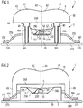
- FIGS. 1 and 2 shown embodiments of a lighting arrangement are preferably provided for the homogeneous illumination of a substantially perpendicular to the optical axis 40 extending surface 80. Since the surface to be illuminated is typically considerably larger than the surface of the semiconductor chip 5, it is conducive to uniform illumination, if possible large part of the radiation generated in the optoelectronic component 2, the radiation exit surface 41 leaves at a large angle to the optical axis.
- the maximum of the radiated radiant power as a function of the angle to the optical axis at an angle of greater than or equal to 50 °, more preferably greater than or equal to 60 °, for example about 70 °.
- FIG. 3 A possible shaping for the beam shaping part 48 of the optical device 4 of such a lighting arrangement 1 and the functioning of the optical device 4 will be described with reference to FIG FIG. 3 explained.
- the structure of the illumination arrangement shown corresponds to that of the Figures 1 and 2 , For reasons of clarity, however, some details of the illumination arrangement which are not critical to the principle of beam shaping of the radiation generated by the semiconductor chip 5 in an active region 51 by the optical device 4 in accordance with a radiation characteristic predetermined for the illumination arrangement are not shown.
- the radiation entrance surface 46 is substantially planar.
- the beam shaping of the radiation generated in the optoelectronic component in accordance with an illumination intensity distribution predetermined for the illumination arrangement is preferably carried out predominantly at the radiation exit area, thereby facilitating reliable beam shaping in a simplified manner.
- the radiation exit surface 41 of the optical device is preferably formed rotationally symmetrical to the optical axis 40 of the optical device 4.
- Parts of the optical device that do not serve the beam shaping, such as in the Figures 1 and 2 each support member 49 shown, may be formed differently from the rotational symmetry.
- the radiation exit surface 41 has a concavely curved portion 42.
- the optical axis 40 of the Optical device 4 passes through the concave curved portion.
- the concave curved portion 42 is surrounded by a convex curved portion 43, in particular completely.
- the surface area of the convexly curved partial area is preferably larger than the area of the concavely curved partial area.
- the convexly curved subregion has a first convexly curved subregion 44 and a second, convexly curved subregion 45.
- the radiation generated in the active region 51 of the semiconductor chip 5 exits through a surface 52 of the semiconductor chip and a side surface 53.
- the effect of the optical device 4 on radiation emerging from the surface is shown by way of example with reference to the beams 60, 61 and 62.
- the optical device acts like a diverging lens. Therefore, radiation incident obliquely to the optical axis 40 or at a non-zero distance parallel to the optical axis on the concave curved portion of the radiation exit surface is refracted away from the optical axis. This advantageously reduces the proportion of radiation which strikes the surface 80 to be illuminated in the region near the optical axis.
- radiation 61 and 62 striking the first 44 and second 45 convexly curved subregions, respectively is refracted away from the optical axis.
- the second convexly curved subregion 45 is preferably more curved than the first convexly curved subregion 44, since radiation 62 impinging on the second subregion can be broken particularly efficiently into large angles to the optical axis.
- the radiation exit surface 41 is executed without angular transitions, ie the entire Radiation exit surface is a differentiable surface at each point, in particular at a transition 47 between the concave curved portion 42 and the convex curved portion 43. Brighter or darker areas caused by angular transitions, such as higher intensity rings on the surface to be illuminated, can thus be advantageously avoided.
- the beam paths in or on the optical device preferably extend essentially totally free of reflection.
- the optical device is preferably designed so that any two rays which emanate from the region of the active region 51 which is penetrated by the optical axis do not intersect after exiting the radiation exit surface 41.
- Intersecting beams may have the effect of localized bundling of radiation so that inhomogeneities in irradiance, such as rings or circles of higher intensity, may form on the illumination surface 80 to be illuminated.
- inhomogeneities in irradiance such as rings or circles of higher intensity
- radiation which undergoes reflection before impinging on the radiation exit surface 41 of the optical device 4 may cause cross-beam paths. This is through the in FIG. 3 registered rays 70, which emerge through the side surfaces 53 of the semiconductor chip 5.
- arrows dotted lines 71 and 72 indicate how the beams would pass after reflection on the reflector-like shaped element, when the reflector-like shaped element 3 is not as described in connection with FIG FIG. 1 described for in the semiconductor chip generated radiation would be specifically absorbent, but would cause, for example due to a metallic coating directed reflection incident radiation.
- the beams 71 would intersect with the beams 60 and the beams 72 with the beams 61 after exiting the radiation exit surface 41. As a result, regions of increased illumination could form on the surface to be illuminated for specific distances of the surface 80 from the radiation exit surface.
- both the beam 71, which would be deflected onto the concavely curved portion 42 of the radiation exit surface 41, and the beam 72, which would hit the convexly curved portion 43, would not be of the optical Axis away, but mainly lead to an illumination of the portion of the surface to be illuminated 80 near the optical axis. This central area of the area would be more illuminated. Also, a reflector-like shaped member made diffusely reflecting with a high reflection coefficient, such as a reflector-like shaped member formed by a white plastic surface, would become more.
- the housing body is preferably designed to be completely absorbent for the entire visible spectral range. Inhomogeneous illumination due to phantom radiation can thus be greatly reduced.
- the substantial reduction of the scattered light component generally facilitates the beam shaping of the radiation generated in the optoelectronic component in accordance with a radiation characteristic predetermined, in particular directed, of the illumination arrangement.
- FIG. 4 an embodiment of a particularly suitable for the optoelectronic component semiconductor chip 5 is shown with reference to a schematic sectional view.
- the semiconductor chip 5 has a semiconductor body 54 arranged on a carrier 55.
- the semiconductor body comprises a semiconductor layer sequence with an active region 51 provided for generating radiation.
- the semiconductor layer sequence forms the semiconductor body 54.
- a first contact 58 is arranged on the side of the semiconductor body remote from the carrier.
- the first contact 58 is in particular for the electrically conductive connection with a bonding wire and the second contact 59 for electrically conductive connection to a connecting conductor.
- the contacts may each contain a metal or an alloy.
- the semiconductor body 54 in particular the active region 51, contains at least one III-V semiconductor material, for example a material from the material systems In x Ga y Al 1-xy P, In x Ga y Al 1-xy N or In x Ga y Al 1-xy As, each with 0 ⁇ x ⁇ 1, 0 ⁇ y ⁇ 1 and x + y ⁇ 1, in particular with x ⁇ 0, y ⁇ 0, x ⁇ 1 and / or y ⁇ 1.
- the semiconductor layer sequence is produced in an epitaxial deposition process, for example by means of MBE or MOVPE on a growth substrate.
- III-V semiconductor materials are used for generating radiation in the ultraviolet (In x Ga y Al 1-xy N) over the visible (In x Ga y Al 1-xy N, in particular for blue to green radiation, or In x Ga y Al 1- xy P, in particular for yellow to red radiation) to the infrared (In x Ga y Al 1-xy As) spectral range is particularly suitable.
- III-V semiconductor materials in particular from the mentioned material systems, it is furthermore possible to achieve advantageously high internal quantum efficiencies in the generation of radiation.
- the active region 51 comprises a heterostructure, in particular a double heterostructure.
- the active zone may comprise a single or a multiple quantum well structure.
- quantum well structure encompasses any structure in which charge carriers can experience or experience quantization of their energy states by confinement.
- quantum well structure does not include information about the dimensionality of the quantization. It thus includes quantum wells, quantum wires and quantum dots and any combination of these structures.
- a mirror layer 56 is arranged on the semiconductor body.
- the mirror layer is arranged between the semiconductor body 54 and the carrier 55.
- the mirror layer can be embodied, for example, as a metal-containing, in particular substantially metallic, mirror layer. Radiation generated in the active region can be reflected at the mirror layer, which prevents absorption in the downstream of the mirror layer from the active region structures, such as the support. The efficiency of the semiconductor chip 5 can thus be increased.
- the mirror layer contains Au, Al, Ag, Pd, Rh, Pt or an alloy with at least one of these materials.
- Al, Pd, Rh and Ag have particularly high reflectivities in the ultraviolet and blue spectral range, Au also in the yellow, orange and red to the infrared spectral range. Furthermore, the proportion of radiation exiting the mirror layer 56 on the side of the semiconductor body is increased by reflection at the mirror layer.
- connection layer 57 may be arranged, by means of which the semiconductor body is fixed on the carrier by the mirror layer.
- the connection layer 307 can be designed, for example, as a solder layer.
- the in FIG. 4 shown semiconductor chip is designed as a thin-film semiconductor chip.
- the carrier is different from a growth substrate on which the semiconductor layer sequence of the semiconductor body is deposited, for example by means of epitaxy.
- the growth substrate may be mechanically and / or chemically removed in regions or completely or thinned.
- the carrier serves for the mechanical stabilization of the semiconductor body.
- the support does not have to meet the stringent crystalline purity requirements, but rather may be selected for other criteria such as mechanical stability, thermal or electrical properties.
- the carrier 55 has a comparatively high thermal conductivity.
- the carrier contains Ge.
- a GaAs-containing carrier can find application.
- the active region 51 is preferably electrically conductively connected to the second contact 59 via the electrically conductive carrier, the electrically conductive connection layer and the electrically conductive mirror layer and the semiconductor layer sequence of the semiconductor body.
- the carrier contains a semiconductor material
- the carrier is preferably suitably doped to increase the conductivity.
- the surface 52 of the semiconductor body facing away from the mirror layer is formed as a main radiation output surface in the illustrated thin-film chip.
- a side surface 53 forms a secondary radiation exit surface.
- the radiation output emerging from the main radiation decoupling surface is greater than the radiation output emerging from the secondary radiation exit surface.
- the sum of the radiation output emerging from the secondary radiation exit surfaces is smaller than the radiation output exiting through the main radiation output surface.
- the radiation output emerging from the lateral secondary radiation exit surfaces reduces in favor of an increased radiation output coupled out of the main radiation output surface. Since, preferably, only the radiation emerging from the surface 52 of the semiconductor chip is to be provided by the illumination arrangement 1, while laterally emerging radiation is used as in connection with FIG FIG. 3 described absorbed by the targeted absorbing formed reflector-like shaped element 3 is predominantly, thus advantageously increases the radiated from the illumination assembly 1 radiant power. Therefore, thin film semiconductor chips are particularly suitable as a radiation source.
- FIG. 4 a semiconductor chip, in which the growth substrate is not detached, may be suitable for the lighting arrangement.
- a semiconductor chip can be used in FIG. 4 have shown construction.
- the carrier 55 is formed by the growth substrate.
- the connection layer 57 is then not required.
- the mirror layer 56 may be omitted or it may be embodied as a Bragg mirror, consisting of a series of layers, for example as part of the semiconductor layer sequence of the semiconductor body 54.
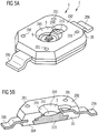
- FIGS. 5A and 5B Another embodiment of a lighting arrangement is in the FIGS. 5A and 5B shown, where FIG. 5A a perspective view and FIG. 5B is a perspective sectional view.
- the illumination arrangement 1 has an optoelectronic component 2, in which a reflector-like-shaped element is formed by a wall 245 of a cavity 240 of a housing body 20 and is designed to be absorbent in a targeted manner for radiation generated in the optoelectronic component.
- a thin-film semiconductor chip 5 serves as a radiation source.
- the cavity 240 is formed as a recess in a first main surface 202 of the housing body 20.
- a bottom 241 of the cavity preferably runs substantially parallel to the first main surface.
- the expansion of the cavity in a plane extending parallel to the first main surface decreases with increasing distance from the first main surface, in particular continuously, so that the bottom of the cavity has a smaller diameter than the diameter of the cavity in the plane of the first main surface.
- the cavity may be substantially the shape of a truncated cone, the diameter of which decreases with increasing distance from the first main surface.
- the optoelectronic component has a thermal connection part 215 on which the semiconductor chip 5 is arranged.
- the thermal connection part extends in the vertical direction with preference from the cavity 240 to a second main surface 204 of the housing body 20.
- the thermal connection part facilitates a large-area, thermal connection of the semiconductor chip 5 on the part of the second main area, in particular with respect to the chip mounting area on the thermal connection part to an external heat-conducting device, such as a heat sink, eg made of Cu.
- the optoelectronic component can be designed to generate a high radiation power at a heat transfer which is advantageously improved at the same time on account of the thermal connection part.
- Such an optoelectronic component is particularly suitable for illuminating surfaces, for example for backlighting a display device, such as an LCD.
- the thermal connection part 215 is inserted, for example, in a tab of a first connection conductor 205, inserted or otherwise with the first connection conductor, in particular electrically conductive and / or mechanically, laterally connected peripherally. Furthermore, the first main surface 202 of the housing body 20 has a recess 213 formed in the wall 245 of the cavity. This recess is provided for an electrically conductive connection of a second electrical connecting conductor 206 to the semiconductor chip 5, for example by means of the bonding wire 290.
- the second terminal conductor 206 is preferably increased in the chip mounting plane of the semiconductor chip 5 on the thermal terminal part 215.
- the thermal connection part can furthermore protrude from the housing body on the part of the second main surface 204 or terminate substantially flush with the housing body.
- the thermal connection part contains a metal of high thermal conductivity, such as Cu or Al, or an alloy, such as a CuW alloy.
- a lead frame having such a formed terminal part and a housing body is in the WO02 / 084749 , described.
- optoelectronic component as an optoelectronic component in the lighting arrangements according to the Figures 1 and 2 be used.
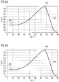
- Figures 6A and 6B It is shown how the radiation characteristic of a lighting arrangement according to the invention in relation to a lighting arrangement in which a reflector-like shaped element is not formed specifically absorbent, advantageously changed.
- the figure shows a first measurement ( FIG.
- FIG. 6A of the intensity I emitted in the visible spectral range in arbitrary units as a function of the angle ⁇ to the optical axis for a first illumination arrangement and a second measurement ( FIG. 6B ) of the radiated intensity I in arbitrary units as a function of the angle ⁇ to the optical axis for a second illumination arrangement.
- the second lighting arrangement is as related to Figures 1 and 2 described executed.
- the first lighting arrangement is constructed identically to the second lighting arrangement, but the reflector-like-shaped element is not specifically designed to be absorbent.
- the housing body 20 of the first lighting arrangement is made of highly reflective plastic, reflectivities of about 85% for the surface of the housing body and thus for the reflector-like shaped element are achieved by adding TiO 2 particles in the plastic composition.
- the housing body and thus the reflector-like shaped element are designed to be absorbent in such a way that the plastic mass from which the housing body is made is colored black by the addition of carbon black-like particles, so that the reflectivity of the housing body in the visible spectral range is about 5 % is.
- a curve 400 shows the course of the intensity of the optical power radiated by the first illumination arrangement as a function of the angle to the optical axis.
- the intensity is normalized to 1 and thus given as relative intensity.
- a curve 450 shows the emission characteristic of the second illumination arrangement, wherein the intensity curve is in turn normalized.
- Both the curve 400 and the curve 450 have an overall maximum 410 or 460 of the intensity at an angle of approximately 67 ° to the optical axis. Accordingly, the described optical device causes that the radiation generated in the optoelectronic component is predominantly not emitted along the optical axis.
- first and the second illumination arrangement essentially differ only by the embodiment of the reflector-like shaped element, radiation which emerges through the respective main radiation coupling-out surface 52 and strikes the radiation exit surface undergoes essentially the same radiation shaping in both illumination arrangements. Differences between the radiation characteristic of the first and the second illumination arrangement therefore arise mainly due to radiation leaving the semiconductor chip in each case through a side surface 53.
- the reflector-like-shaped element 3 due to its shape and arrangement relative to the radiation-generating semiconductor chip, is suitable for deflecting at least part of the radiation striking the reflector-like shaped element onto the radiation exit surface 41. Because of the comparatively high reflectivity of about 85%, therefore, a considerable part of the radiation emerging from the side surfaces 53 can be deflected onto the radiation exit surface 41 of the optical device 4.
- the reflector-like shaped element is specifically designed to absorb the radiation generated in the semiconductor chip so that the reflector-like shaped element, due to the low reflectivity of about 5%, despite its shape and arrangement, only a significantly smaller portion of one of the side surfaces 53 Exiting radiation deflects to the radiation exit surface.
- the relative intensity 400 of the radiation 420 emitted by the first illumination arrangement is significantly higher than the relative intensity of that of the second one Illumination arrangement in the corresponding area 430 emitted radiation.
- This will, as related to FIG. 3 described, caused by scattered radiation, which is directed by the reflector-like shaped element on the radiation exit surface and exit therefrom mainly at angles to the optical axis 40, which are considerably smaller than 60 °, about 40 ° or smaller.
- a radiation characteristic with a maximum at angles of 60 ° or greater with simultaneous additional reduction of radiated into small angles to the optical axis 40 radiant power can thus be achieved improved by the targeted absorbent design of the reflector-like shaped element.
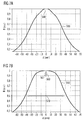
- FIGS. 7A and 7B The illuminance distributions shown were performed on the same components as those in Figures 6A and 6B shown measurements.
- Figure 7A and Figure 7B each show the illumination intensity distribution for the first and second illumination arrangement.
- Both the curve 500 for the first illumination arrangement and the curve 550 for the second illumination arrangement represent the illuminance B along a straight line which is perpendicular to the optical axis 4 at a distance of 25 mm above the surface of the semiconductor chip 5 from the radiation exit surface 41 of the optical device 4 40 runs.
- the distance d from the intersection of this line with the optical axis plotted on a mm scale On the x-axis, the distance d from the intersection of this line with the optical axis plotted on a mm scale.
- the illumination intensity is normalized for the two curves 500 and 550 to the respective maximum value, which both curves assume at the point of intersection with the optical axis, and indicated in a relative scale in arbitrary units.
- the two illuminance distributions 500 and 550 are substantially symmetrical with respect to the y-axis.
- the reflector-like element of high reflectivity In the first illumination arrangement, radiation emerging from the side surfaces can be deflected by the reflector-like element of high reflectivity onto the radiation exit surface 41. This radiation component strikes the radiation exit surface at an angle which is difficult to control and can therefore only be formed with difficulty by the optical device 4 in accordance with the emission characteristic predetermined by the illumination arrangement. The deflection is predominantly in comparatively small angles to the optical axis, which leads to an inflated in the range 510 illuminance.
- the reflector-like-shaped element is designed to be absorbent so that radiation emerging from the side surface 53 of the semiconductor chip is predominantly absorbed.
- a common parameter for the width of a distribution is the full width of the half width, which indicates how wide the range around the maximum of the distribution is, in which the function value of the distribution is 50% or more of the maximum function value.
- this width is indicated by a horizontal arrow 570.
- the full half width of the curve 550 is advantageously widened over that of the curve 500 to about 84 mm versus 76 mm in the curve 500.
- the illumination intensity distribution can advantageously be widened significantly by means of a targeted absorptively formed reflector-like shaped element.
- an area which is considerably larger than the surface 52 of the semiconductor chip 5 be illuminated particularly homogeneous.
- the second illumination arrangement described is particularly suitable for the backlighting of display devices such as LCDs. Due to the large-area illumination at small intervals of the surface to be illuminated by the illumination arrangement, the depth of the backlight unit can be advantageously kept low.
- such a lighting arrangement can be used, for example, for general lighting, effect lighting, illumination of neon signs or for channel letters.
Landscapes
- Engineering & Computer Science (AREA)
- Physics & Mathematics (AREA)
- Microelectronics & Electronic Packaging (AREA)
- General Physics & Mathematics (AREA)
- Optics & Photonics (AREA)
- Manufacturing & Machinery (AREA)
- Computer Hardware Design (AREA)
- Power Engineering (AREA)
- Led Device Packages (AREA)
- Planar Illumination Modules (AREA)
- Led Devices (AREA)
- Non-Portable Lighting Devices Or Systems Thereof (AREA)
Claims (15)
- Dispositif d'éclairage (1) comprenant un dispositif optique (4) présentant une surface de sortie de rayonnement (41) et un composant optoélectronique (2) pour générer un rayonnement, dans lequel- un élément (3) est conçu en forme de réflecteur, dont la forme et l'agencement sont appropriés pour dévier le rayonnement généré dans le composant à travers la surface de sortie du rayonnement,- le composant optoélectronique (2) est conçu sous la forme d'un composant CMS montable en surface ; et- l'élément en forme de réflecteur (3) est spécifiquement conçu pour absorber le rayonnement généré dans le composant ; sur lequel- le composant optoélectronique (2) contient l'élément conçu en forme de réflecteur et spécifiquement absorbant ; et- le composant optoélectronique (2) comprend au moins une puce semi-conductrice (5) appropriée pour générer un rayonnement ;caractérisé en ce que
la réflectivité de l'élément en forme de réflecteur (3) pour le rayonnement généré dans le composant (2) est de 15 % ou moins ; et
la puce semi-conductrice est formée sous la forme d'une puce semi-conductrice à couche mince, dans laquelle le corps semiconducteur est disposé sur un support différent d'un substrat de croissance. - Dispositif d'éclairage selon la revendication 1, sur lequel la surface de sortie de rayonnement (41) présente une partie incurvée concave (42) et une partie incurvée convexe (43) entourant au moins partiellement la partie incurvée concave.
- Dispositif d'éclairage selon la revendication 1 ou 2, dans lequel
le dispositif optique (4) est fixé au composant optoélectronique (2). - Dispositif d'éclairage selon l'une des revendications précédentes, sur lequel une distance minimale entre la surface de sortie de rayonnement (41) et la puce semi-conductrice (5) est inférieure ou égale à 5 mm.
- Dispositif d'éclairage selon l'une des revendications précédentes, sur lequel une distance minimale entre la surface de sortie de rayonnement (41) et la puce semi-conductrice (5) est inférieure ou égale à 3mm.
- Dispositif d'éclairage selon l'une des revendications précédentes, sur lequel le dispositif optique (4) est conçu pour former une caractéristique de rayonnement prédéfinie du dispositif d'éclairage, dans lequel un impact du rayonnement découplé hors de la puce semi-conductrice (5) après réflexion à l'intérieur du dispositif d'éclairage sur la surface de sortie de rayonnement (41) est au moins partiellement réprimé.
- Dispositif d'éclairage selon l'une des revendications précédentes,
la puce semi-conductrice (5) présentant une surface (52) conçue en tant que surface de découplage du rayonnement principal et une surface latérale (53) formant une surface de sortie de rayonnement secondaire, la forme et l'agencement de l'élément en forme de réflecteur (3) permettant de dévier au moins une partie du rayonnement sortant de la surface de sortie de rayonnement secondaire. - Dispositif d'éclairage selon l'une des revendications précédentes,
sur lequel la puce semi-conductrice (5) comprend un corps semi-conducteur (54) doté d'une succession de couches semi-conductrices présentant une zone active (51) prévue pour générer un rayonnement et un support (55),
le corps semi-conducteur étant disposé sur le support et le support étant différent d'un substrat de croissance de la succession de couches semi-conductrices. - Dispositif d'éclairage selon la revendication 8,
sur lequel une couche miroir (56) est disposée entre le corps semi-conducteur (54) et le support (55), la couche miroir (56) contenant un métal ou étant métallique. - Dispositif d'éclairage selon l'une des revendications 1 à 9,
sur lequel le composant optoélectronique comprend un corps de boîtier (20) et un conducteur de connexion électrique externe (205), le boîtier contenant l'élément en forme de réflecteur (3) et la puce semi-conductrice (5) étant fixée au conducteur de connexion. - Dispositif d'éclairage selon la revendication 10,
sur lequel l'élément en forme de réflecteur (3) est conçu au moyen d'une paroi (245) d'une cavité (240) du corps de boîtier (20), la puce semi-conductrice (5) étant disposée dans la cavité (240) du corps de boîtier (20). - Dispositif d'éclairage selon la revendication 10 ou 11,
sur lequel le corps du boîtier (20) est en céramique noire ou sur lequel le corps du boîtier contient une céramique et est noirci. - Dispositif d'éclairage selon la revendication 10 ou 11,
sur lequel le corps du boîtier (20) est en plastique noir ou sur lequel le corps du boîtier contient une matière plastique et est noirci. - Dispositif d'éclairage selon l'une des revendications 1 à 13,
sur lequel l'élément en forme de réflecteur (3) est au moins partiellement constitué d'un matériau noir ou d'un composé de matériaux noirs ou au moins partiellement pourvu d'un matériau noir ou d'un composé de matériaux noirs. - Dispositif d'éclairage selon l'une des revendications précédentes,
sur lequel le dispositif d'éclairage est prévu pour le rétroéclairage d'un dispositif d'affichage, tel qu'un écran LCD.
Applications Claiming Priority (2)
| Application Number | Priority Date | Filing Date | Title |
|---|---|---|---|
| DE102006035635A DE102006035635A1 (de) | 2006-07-31 | 2006-07-31 | Beleuchtungsanordnung |
| PCT/DE2007/001348 WO2008014771A1 (fr) | 2006-07-31 | 2007-07-27 | Ensemble d'éclairage |
Publications (2)
| Publication Number | Publication Date |
|---|---|
| EP2047526A1 EP2047526A1 (fr) | 2009-04-15 |
| EP2047526B1 true EP2047526B1 (fr) | 2018-07-25 |
Family
ID=38692073
Family Applications (1)
| Application Number | Title | Priority Date | Filing Date |
|---|---|---|---|
| EP07817414.1A Active EP2047526B1 (fr) | 2006-07-31 | 2007-07-27 | Ensemble d'éclairage |
Country Status (8)
| Country | Link |
|---|---|
| US (1) | US8585252B2 (fr) |
| EP (1) | EP2047526B1 (fr) |
| JP (2) | JP5675101B2 (fr) |
| KR (1) | KR101314414B1 (fr) |
| CN (1) | CN101496189B (fr) |
| DE (1) | DE102006035635A1 (fr) |
| TW (1) | TWI396309B (fr) |
| WO (1) | WO2008014771A1 (fr) |
Families Citing this family (29)
| Publication number | Priority date | Publication date | Assignee | Title |
|---|---|---|---|---|
| WO2009157166A1 (fr) * | 2008-06-23 | 2009-12-30 | パナソニック株式会社 | Appareil électroluminescent, appareil plan électroluminescent et appareil d'affichage |
| DE102008045653B4 (de) | 2008-09-03 | 2020-03-26 | Osram Opto Semiconductors Gmbh | Optoelektronisches Bauteil |
| US8083380B2 (en) * | 2009-04-17 | 2011-12-27 | Mig Technology Inc. | Integrated structure for optical refractor |
| TWI384177B (zh) * | 2009-09-04 | 2013-02-01 | Au Optronics Corp | 具高發光效率之光源裝置及其製造方法 |
| JP5263788B2 (ja) * | 2009-10-22 | 2013-08-14 | シャープ株式会社 | 表示装置 |
| CN102054920A (zh) * | 2009-10-27 | 2011-05-11 | 展晶科技(深圳)有限公司 | 发光二极管封装结构 |
| US8602605B2 (en) | 2010-01-07 | 2013-12-10 | Seoul Semiconductor Co., Ltd. | Aspherical LED lens and light emitting device including the same |
| US20110273892A1 (en) * | 2010-05-07 | 2011-11-10 | Tyco Electronics Corporation | Solid state lighting assembly |
| CN104154463A (zh) * | 2010-09-27 | 2014-11-19 | 北京京东方光电科技有限公司 | 发光二极管光源及其制造方法、具有其的背光源 |
| DE102010048162A1 (de) | 2010-10-11 | 2012-04-12 | Osram Opto Semiconductors Gmbh | Konversionsbauteil |
| RU2612562C2 (ru) | 2011-05-05 | 2017-03-09 | Филипс Лайтинг Холдинг Б.В. | Оптическое устройство для формирования светового пучка |
| KR101978634B1 (ko) * | 2012-07-27 | 2019-05-15 | 엘지이노텍 주식회사 | 조명기기 |
| CN104235754B (zh) * | 2013-06-20 | 2019-06-18 | 欧司朗有限公司 | 用于照明装置的透镜和具有该透镜的照明装置 |
| TW201508220A (zh) * | 2013-08-27 | 2015-03-01 | Hon Hai Prec Ind Co Ltd | 發光二極體模組 |
| JP6323020B2 (ja) | 2014-01-20 | 2018-05-16 | セイコーエプソン株式会社 | 光源装置およびプロジェクター |
| JP6374723B2 (ja) * | 2014-07-25 | 2018-08-15 | スタンレー電気株式会社 | 半導体発光装置 |
| DE102015101216A1 (de) * | 2015-01-28 | 2016-07-28 | Osram Opto Semiconductors Gmbh | Optoelektronische Anordnung mit Strahlungskonversionselement und Verfahren zur Herstellung eines Strahlungskonversionselements |
| USD779112S1 (en) | 2015-04-24 | 2017-02-14 | Abl Ip Holding Llc | Tri-lobe light fixture optic |
| US10393341B2 (en) | 2015-04-24 | 2019-08-27 | Abl Ip Holding Llc | Tri-lobe optic and associated light fixtures |
| DE102015112042B4 (de) | 2015-07-23 | 2021-07-01 | OSRAM Opto Semiconductors Gesellschaft mit beschränkter Haftung | Optoelektronische Leuchtvorrichtung |
| WO2017061370A1 (fr) * | 2015-10-07 | 2017-04-13 | 株式会社エンプラス | Élément de commande de flux lumineux, dispositif électroluminescent, dispositif de source de lumière de surface et dispositif d'affichage |
| JP6110528B2 (ja) * | 2016-02-03 | 2017-04-05 | 京セラコネクタプロダクツ株式会社 | 半導体発光素子用ホルダ、及び、半導体発光素子モジュール |
| WO2018147963A1 (fr) * | 2017-02-08 | 2018-08-16 | Princeton Optronics, Inc. | Boîtier d'éclairage vcsel comprenant une structure optique intégrée dans l'encapsulant |
| CN110594704B (zh) | 2018-06-12 | 2021-10-29 | 意法半导体(格勒诺布尔2)公司 | 光源的保护机构 |
| US10865962B2 (en) * | 2018-06-12 | 2020-12-15 | Stmicroelectronics (Grenoble 2) Sas | Protection mechanism for light source |
| CN210118715U (zh) | 2018-06-12 | 2020-02-28 | 意法半导体(格勒诺布尔2)公司 | 用于安装在基板上的光源的壳体和电子设备 |
| US10738985B2 (en) | 2018-06-12 | 2020-08-11 | Stmicroelectronics (Research & Development) Limited | Housing for light source |
| FR3085465B1 (fr) | 2018-08-31 | 2021-05-21 | St Microelectronics Grenoble 2 | Mecanisme de protection pour source lumineuse |
| KR102543767B1 (ko) * | 2020-11-26 | 2023-06-16 | 주식회사 사이언 | 야시조명계통용 발광다이오드 |
Citations (3)
| Publication number | Priority date | Publication date | Assignee | Title |
|---|---|---|---|---|
| WO2003049204A2 (fr) * | 2001-11-30 | 2003-06-12 | Osram Opto Semiconductors Gmbh | Composant optoelectronique |
| US20040037076A1 (en) * | 2002-07-17 | 2004-02-26 | Sharp Kabushiki Kaisha | Light emitting diode lamp and light emitting diode display unit |
| JP2006013265A (ja) * | 2004-06-28 | 2006-01-12 | Kyocera Corp | 発光装置およびそれを用いた照明装置 |
Family Cites Families (22)
| Publication number | Priority date | Publication date | Assignee | Title |
|---|---|---|---|---|
| JPS63178569A (ja) * | 1987-01-20 | 1988-07-22 | Toshiba Corp | 半導体発光装置 |
| DE8713875U1 (de) | 1987-10-15 | 1988-02-18 | Siemens AG, 1000 Berlin und 8000 München | Optisches Senderbauelement |
| JPH01258481A (ja) * | 1988-04-08 | 1989-10-16 | Toshiba Corp | Ledアレイ |
| JPH02306289A (ja) * | 1989-05-22 | 1990-12-19 | Rohm Co Ltd | 発光ダイオード |
| AUPM483294A0 (en) * | 1994-03-31 | 1994-04-28 | Chulalongkorn University | Amorphous semiconductor thin film light emitting diode |
| DE19738972A1 (de) * | 1997-08-11 | 1999-02-18 | Man Technologie Gmbh | Displayanordnung zum Anzeigen von Informationen und deren Verwendung |
| US6340824B1 (en) * | 1997-09-01 | 2002-01-22 | Kabushiki Kaisha Toshiba | Semiconductor light emitting device including a fluorescent material |
| JP2001242356A (ja) * | 2000-02-28 | 2001-09-07 | Alps Electric Co Ltd | 光ファイバコネクタ及びそれを用いた光通信モジュール |
| JP4050444B2 (ja) * | 2000-05-30 | 2008-02-20 | 信越半導体株式会社 | 発光素子及びその製造方法 |
| CN1177377C (zh) | 2000-09-01 | 2004-11-24 | 西铁城电子股份有限公司 | 表面装配型发光二极管及其制造方法 |
| TW528889B (en) * | 2000-11-14 | 2003-04-21 | Toshiba Corp | Image pickup apparatus, manufacturing method thereof, and portable electric apparatus |
| EP1227458A3 (fr) * | 2001-01-11 | 2004-12-22 | Dr. techn. Josef Zelisko, Fabrik für Elektrotechnik und Maschinenbau Gesellschaft m.b.H. | Dispositif d' affichage et /ou de signalisation |
| DE10117889A1 (de) | 2001-04-10 | 2002-10-24 | Osram Opto Semiconductors Gmbh | Leiterrahmen und Gehäuse für ein strahlungsemittierendes Bauelement, strahlungsemittierendes Bauelement sowie Verfahren zu dessen Herstellung |
| US6820991B2 (en) * | 2001-05-14 | 2004-11-23 | Nichia Corporation | Light emitting device and vehicle display device |
| DE10344768B3 (de) * | 2003-09-26 | 2005-08-18 | Siemens Ag | Optisches Modul mit federndem Element zwischen Linsenhalter und Schaltungsträger und optisches System |
| DE102005016592A1 (de) | 2004-04-14 | 2005-11-24 | Osram Opto Semiconductors Gmbh | Leuchtdiodenchip |
| KR101085144B1 (ko) | 2004-04-29 | 2011-11-21 | 엘지디스플레이 주식회사 | Led 램프 유닛 |
| JP3875247B2 (ja) | 2004-09-27 | 2007-01-31 | 株式会社エンプラス | 発光装置、面光源装置、表示装置及び光束制御部材 |
| JP2006100500A (ja) | 2004-09-29 | 2006-04-13 | Sanken Electric Co Ltd | 半導体発光素子及びその製造方法 |
| KR101080355B1 (ko) | 2004-10-18 | 2011-11-04 | 삼성전자주식회사 | 발광다이오드와 그 렌즈 |
| US20060082297A1 (en) * | 2004-10-19 | 2006-04-20 | Eastman Kodak Company | Method of preparing a lens-less LED |
| JP2006186158A (ja) | 2004-12-28 | 2006-07-13 | Sharp Corp | 発光ダイオードランプおよび発光ダイオード表示装置 |
-
2006
- 2006-07-31 DE DE102006035635A patent/DE102006035635A1/de not_active Withdrawn
-
2007
- 2007-07-27 US US12/375,530 patent/US8585252B2/en active Active
- 2007-07-27 EP EP07817414.1A patent/EP2047526B1/fr active Active
- 2007-07-27 CN CN200780028740.4A patent/CN101496189B/zh active Active
- 2007-07-27 KR KR1020097002782A patent/KR101314414B1/ko active IP Right Grant
- 2007-07-27 WO PCT/DE2007/001348 patent/WO2008014771A1/fr active Application Filing
- 2007-07-27 JP JP2009522084A patent/JP5675101B2/ja active Active
- 2007-07-30 TW TW096127686A patent/TWI396309B/zh active
-
2014
- 2014-10-09 JP JP2014208110A patent/JP6141248B2/ja active Active
Patent Citations (3)
| Publication number | Priority date | Publication date | Assignee | Title |
|---|---|---|---|---|
| WO2003049204A2 (fr) * | 2001-11-30 | 2003-06-12 | Osram Opto Semiconductors Gmbh | Composant optoelectronique |
| US20040037076A1 (en) * | 2002-07-17 | 2004-02-26 | Sharp Kabushiki Kaisha | Light emitting diode lamp and light emitting diode display unit |
| JP2006013265A (ja) * | 2004-06-28 | 2006-01-12 | Kyocera Corp | 発光装置およびそれを用いた照明装置 |
Also Published As
| Publication number | Publication date |
|---|---|
| JP2015015260A (ja) | 2015-01-22 |
| KR101314414B1 (ko) | 2013-10-04 |
| US20100073907A1 (en) | 2010-03-25 |
| WO2008014771A1 (fr) | 2008-02-07 |
| JP6141248B2 (ja) | 2017-06-07 |
| CN101496189B (zh) | 2014-06-18 |
| EP2047526A1 (fr) | 2009-04-15 |
| JP2009545864A (ja) | 2009-12-24 |
| KR20090034966A (ko) | 2009-04-08 |
| TWI396309B (zh) | 2013-05-11 |
| JP5675101B2 (ja) | 2015-02-25 |
| DE102006035635A1 (de) | 2008-02-07 |
| TW200814376A (en) | 2008-03-16 |
| US8585252B2 (en) | 2013-11-19 |
| CN101496189A (zh) | 2009-07-29 |
Similar Documents
| Publication | Publication Date | Title |
|---|---|---|
| EP2047526B1 (fr) | Ensemble d'éclairage | |
| EP1352432B9 (fr) | Diode luminescente et procede permettant de la produire | |
| EP1771891B1 (fr) | Element électroluminescent et module lumineux | |
| EP1792351B1 (fr) | Boitier pour un composant optoelectronique, composant optoelectronique et procede de production de ce dernier | |
| EP1864340B1 (fr) | Dispositif d'éclairage | |
| DE102012102114B4 (de) | Strahlungsemittierendes Halbleiterbauteil, Beleuchtungsvorrichtung und Anzeigevorrichtung | |
| DE19942470B4 (de) | Optisches Halbeitermodul und Verfahren zum Herstellen eines optischen Halbleitermoduls | |
| EP2583319B1 (fr) | Composant optoélectronique | |
| EP1805813B1 (fr) | Dispositif a semiconducteur emettant un rayonnement electromagnetique | |
| EP1982360B1 (fr) | Diode électroluminescente comprenant un boîtier | |
| DE112013000928B4 (de) | Optoelektronisches Halbleiterbauelement | |
| EP1597776A2 (fr) | Module d'eclairage et procede de fabrication | |
| EP1905287B1 (fr) | Boitier pour composant optoélectronique émettant du rayonnement électromagnétique, composant émettant du rayonnement électromagnétique, et procédé pour réaliser un boitier ou un composant de ce type | |
| DE102006046037B4 (de) | LED-Halbleiterkörper und Verwendung eines LED-Halbleiterkörpers | |
| DE102005019832A1 (de) | Beleuchtungsvorrichtung | |
| DE102011080458A1 (de) | Optoelektronische anordnung und verfahren zur herstellung einer optoelektronischen anordnung | |
| DE102017111706A1 (de) | Lichtemissionsvorrichtung | |
| WO2019076890A1 (fr) | Composant électroluminescent | |
| EP1627455A2 (fr) | Procede de production d'un composant a diodes laser, boitier pour composant a diodes laser, et composant a diodes laser y relatif | |
| DE112017001296B4 (de) | Halbleiterlichtquelle | |
| DE112018001199B4 (de) | Optoelektronisches Halbleiterbauteil | |
| DE10345516B4 (de) | Elektromagnetische Strahlung aussendendes Halbleiterbauelement und Verfahren zu seiner Herstellung | |
| EP0839400B1 (fr) | Puce laser a semi-conducteur et composant emetteur d'infrarouges | |
| WO2017178421A1 (fr) | Puce semiconductrice électroluminescente, composant électroluminescent et procédé de fabrication d'un composant électroluminescent |
Legal Events
| Date | Code | Title | Description |
|---|---|---|---|
| PUAI | Public reference made under article 153(3) epc to a published international application that has entered the european phase |
Free format text: ORIGINAL CODE: 0009012 |
|
| 17P | Request for examination filed |
Effective date: 20081222 |
|
| AK | Designated contracting states |
Kind code of ref document: A1 Designated state(s): AT BE BG CH CY CZ DE DK EE ES FI FR GB GR HU IE IS IT LI LT LU LV MC MT NL PL PT RO SE SI SK TR |
|
| AX | Request for extension of the european patent |
Extension state: AL BA HR MK RS |
|
| DAX | Request for extension of the european patent (deleted) | ||
| RBV | Designated contracting states (corrected) |
Designated state(s): DE |
|
| 17Q | First examination report despatched |
Effective date: 20150401 |
|
| REG | Reference to a national code |
Ref country code: DE Ref legal event code: R079 Ref document number: 502007016303 Country of ref document: DE Free format text: PREVIOUS MAIN CLASS: H01L0033000000 Ipc: H01L0033580000 |
|
| GRAP | Despatch of communication of intention to grant a patent |
Free format text: ORIGINAL CODE: EPIDOSNIGR1 |
|
| RIC1 | Information provided on ipc code assigned before grant |
Ipc: H01L 33/60 20100101ALN20180305BHEP Ipc: H01L 33/44 20100101ALN20180305BHEP Ipc: H01L 33/58 20100101AFI20180305BHEP |
|
| INTG | Intention to grant announced |
Effective date: 20180404 |
|
| GRAS | Grant fee paid |
Free format text: ORIGINAL CODE: EPIDOSNIGR3 |
|
| GRAA | (expected) grant |
Free format text: ORIGINAL CODE: 0009210 |
|
| AK | Designated contracting states |
Kind code of ref document: B1 Designated state(s): DE |
|
| REG | Reference to a national code |
Ref country code: DE Ref legal event code: R096 Ref document number: 502007016303 Country of ref document: DE |
|
| REG | Reference to a national code |
Ref country code: DE Ref legal event code: R097 Ref document number: 502007016303 Country of ref document: DE |
|
| PLBE | No opposition filed within time limit |
Free format text: ORIGINAL CODE: 0009261 |
|
| STAA | Information on the status of an ep patent application or granted ep patent |
Free format text: STATUS: NO OPPOSITION FILED WITHIN TIME LIMIT |
|
| 26N | No opposition filed |
Effective date: 20190426 |
|
| P01 | Opt-out of the competence of the unified patent court (upc) registered |
Effective date: 20230825 |
|
| PGFP | Annual fee paid to national office [announced via postgrant information from national office to epo] |
Ref country code: DE Payment date: 20230719 Year of fee payment: 17 |