EP2047526B1 - Lighting assembly - Google Patents
Lighting assembly Download PDFInfo
- Publication number
- EP2047526B1 EP2047526B1 EP07817414.1A EP07817414A EP2047526B1 EP 2047526 B1 EP2047526 B1 EP 2047526B1 EP 07817414 A EP07817414 A EP 07817414A EP 2047526 B1 EP2047526 B1 EP 2047526B1
- Authority
- EP
- European Patent Office
- Prior art keywords
- radiation
- semiconductor chip
- lighting arrangement
- reflector
- arrangement according
- Prior art date
- Legal status (The legal status is an assumption and is not a legal conclusion. Google has not performed a legal analysis and makes no representation as to the accuracy of the status listed.)
- Active
Links
- 230000005855 radiation Effects 0.000 claims description 249
- 239000004065 semiconductor Substances 0.000 claims description 167
- 230000003287 optical effect Effects 0.000 claims description 142
- 230000005693 optoelectronics Effects 0.000 claims description 90
- 239000000463 material Substances 0.000 claims description 34
- 239000010409 thin film Substances 0.000 claims description 27
- 230000002745 absorbent Effects 0.000 claims description 21
- 239000002250 absorbent Substances 0.000 claims description 21
- 239000004020 conductor Substances 0.000 claims description 21
- 239000004033 plastic Substances 0.000 claims description 16
- 229920003023 plastic Polymers 0.000 claims description 16
- 239000000758 substrate Substances 0.000 claims description 16
- 238000002310 reflectometry Methods 0.000 claims description 13
- 239000000203 mixture Substances 0.000 claims description 10
- 239000000919 ceramic Substances 0.000 claims description 8
- 229910052751 metal Inorganic materials 0.000 claims description 8
- 239000002184 metal Substances 0.000 claims description 7
- 238000004519 manufacturing process Methods 0.000 claims description 3
- 238000005286 illumination Methods 0.000 description 73
- 239000010410 layer Substances 0.000 description 63
- 238000007493 shaping process Methods 0.000 description 20
- 230000003595 spectral effect Effects 0.000 description 11
- 238000009826 distribution Methods 0.000 description 9
- 238000005253 cladding Methods 0.000 description 8
- 229910045601 alloy Inorganic materials 0.000 description 6
- 239000000956 alloy Substances 0.000 description 6
- 239000002131 composite material Substances 0.000 description 6
- 229920001296 polysiloxane Polymers 0.000 description 6
- 238000010521 absorption reaction Methods 0.000 description 5
- 229910052782 aluminium Inorganic materials 0.000 description 5
- 238000013461 design Methods 0.000 description 5
- 238000005259 measurement Methods 0.000 description 5
- 239000002245 particle Substances 0.000 description 5
- 239000000975 dye Substances 0.000 description 4
- 230000009467 reduction Effects 0.000 description 4
- 229910052709 silver Inorganic materials 0.000 description 4
- 239000011358 absorbing material Substances 0.000 description 3
- 230000007423 decrease Effects 0.000 description 3
- 230000000694 effects Effects 0.000 description 3
- 238000004020 luminiscence type Methods 0.000 description 3
- 229910052763 palladium Inorganic materials 0.000 description 3
- 229910052703 rhodium Inorganic materials 0.000 description 3
- 229910000679 solder Inorganic materials 0.000 description 3
- 230000007704 transition Effects 0.000 description 3
- 230000008901 benefit Effects 0.000 description 2
- 230000015572 biosynthetic process Effects 0.000 description 2
- 239000012876 carrier material Substances 0.000 description 2
- 150000001875 compounds Chemical class 0.000 description 2
- 238000005538 encapsulation Methods 0.000 description 2
- 238000000407 epitaxy Methods 0.000 description 2
- 229910052737 gold Inorganic materials 0.000 description 2
- 230000005484 gravity Effects 0.000 description 2
- 229910052738 indium Inorganic materials 0.000 description 2
- 229910052697 platinum Inorganic materials 0.000 description 2
- 229920000642 polymer Polymers 0.000 description 2
- 238000013139 quantization Methods 0.000 description 2
- 238000005476 soldering Methods 0.000 description 2
- 230000006641 stabilisation Effects 0.000 description 2
- 238000011105 stabilization Methods 0.000 description 2
- OKTJSMMVPCPJKN-UHFFFAOYSA-N Carbon Chemical compound [C] OKTJSMMVPCPJKN-UHFFFAOYSA-N 0.000 description 1
- 229910001218 Gallium arsenide Inorganic materials 0.000 description 1
- 229910010413 TiO 2 Inorganic materials 0.000 description 1
- 238000013459 approach Methods 0.000 description 1
- 229910052799 carbon Inorganic materials 0.000 description 1
- 239000002800 charge carrier Substances 0.000 description 1
- 238000006243 chemical reaction Methods 0.000 description 1
- 239000011248 coating agent Substances 0.000 description 1
- 238000000576 coating method Methods 0.000 description 1
- 238000000748 compression moulding Methods 0.000 description 1
- 238000010276 construction Methods 0.000 description 1
- 229910052802 copper Inorganic materials 0.000 description 1
- 230000008878 coupling Effects 0.000 description 1
- 238000010168 coupling process Methods 0.000 description 1
- 238000005859 coupling reaction Methods 0.000 description 1
- 230000001419 dependent effect Effects 0.000 description 1
- 238000005137 deposition process Methods 0.000 description 1
- 238000005530 etching Methods 0.000 description 1
- 238000001746 injection moulding Methods 0.000 description 1
- 239000011229 interlayer Substances 0.000 description 1
- 238000003698 laser cutting Methods 0.000 description 1
- 239000004973 liquid crystal related substance Substances 0.000 description 1
- 238000002488 metal-organic chemical vapour deposition Methods 0.000 description 1
- 238000000034 method Methods 0.000 description 1
- 238000012986 modification Methods 0.000 description 1
- 230000004048 modification Effects 0.000 description 1
- 238000000465 moulding Methods 0.000 description 1
- 238000010137 moulding (plastic) Methods 0.000 description 1
- 229910052754 neon Inorganic materials 0.000 description 1
- GKAOGPIIYCISHV-UHFFFAOYSA-N neon atom Chemical compound [Ne] GKAOGPIIYCISHV-UHFFFAOYSA-N 0.000 description 1
- 230000008569 process Effects 0.000 description 1
- 239000002096 quantum dot Substances 0.000 description 1
- 229920005989 resin Polymers 0.000 description 1
- 239000011347 resin Substances 0.000 description 1
- 229920002050 silicone resin Polymers 0.000 description 1
- 238000004544 sputter deposition Methods 0.000 description 1
- 229920001169 thermoplastic Polymers 0.000 description 1
- 229920001187 thermosetting polymer Polymers 0.000 description 1
- 239000004416 thermosoftening plastic Substances 0.000 description 1
- 238000012549 training Methods 0.000 description 1
- 238000012546 transfer Methods 0.000 description 1
- 238000001721 transfer moulding Methods 0.000 description 1
- 238000007740 vapor deposition Methods 0.000 description 1
Images

Classifications
-
- H—ELECTRICITY
- H01—ELECTRIC ELEMENTS
- H01L—SEMICONDUCTOR DEVICES NOT COVERED BY CLASS H10
- H01L33/00—Semiconductor devices with at least one potential-jump barrier or surface barrier specially adapted for light emission; Processes or apparatus specially adapted for the manufacture or treatment thereof or of parts thereof; Details thereof
- H01L33/48—Semiconductor devices with at least one potential-jump barrier or surface barrier specially adapted for light emission; Processes or apparatus specially adapted for the manufacture or treatment thereof or of parts thereof; Details thereof characterised by the semiconductor body packages
- H01L33/58—Optical field-shaping elements
-
- G—PHYSICS
- G02—OPTICS
- G02B—OPTICAL ELEMENTS, SYSTEMS OR APPARATUS
- G02B3/00—Simple or compound lenses
- G02B3/02—Simple or compound lenses with non-spherical faces
- G02B3/04—Simple or compound lenses with non-spherical faces with continuous faces that are rotationally symmetrical but deviate from a true sphere, e.g. so called "aspheric" lenses
-
- H—ELECTRICITY
- H01—ELECTRIC ELEMENTS
- H01L—SEMICONDUCTOR DEVICES NOT COVERED BY CLASS H10
- H01L2224/00—Indexing scheme for arrangements for connecting or disconnecting semiconductor or solid-state bodies and methods related thereto as covered by H01L24/00
- H01L2224/01—Means for bonding being attached to, or being formed on, the surface to be connected, e.g. chip-to-package, die-attach, "first-level" interconnects; Manufacturing methods related thereto
- H01L2224/26—Layer connectors, e.g. plate connectors, solder or adhesive layers; Manufacturing methods related thereto
- H01L2224/31—Structure, shape, material or disposition of the layer connectors after the connecting process
- H01L2224/32—Structure, shape, material or disposition of the layer connectors after the connecting process of an individual layer connector
- H01L2224/321—Disposition
- H01L2224/32151—Disposition the layer connector connecting between a semiconductor or solid-state body and an item not being a semiconductor or solid-state body, e.g. chip-to-substrate, chip-to-passive
- H01L2224/32221—Disposition the layer connector connecting between a semiconductor or solid-state body and an item not being a semiconductor or solid-state body, e.g. chip-to-substrate, chip-to-passive the body and the item being stacked
- H01L2224/32245—Disposition the layer connector connecting between a semiconductor or solid-state body and an item not being a semiconductor or solid-state body, e.g. chip-to-substrate, chip-to-passive the body and the item being stacked the item being metallic
-
- H—ELECTRICITY
- H01—ELECTRIC ELEMENTS
- H01L—SEMICONDUCTOR DEVICES NOT COVERED BY CLASS H10
- H01L2224/00—Indexing scheme for arrangements for connecting or disconnecting semiconductor or solid-state bodies and methods related thereto as covered by H01L24/00
- H01L2224/01—Means for bonding being attached to, or being formed on, the surface to be connected, e.g. chip-to-package, die-attach, "first-level" interconnects; Manufacturing methods related thereto
- H01L2224/42—Wire connectors; Manufacturing methods related thereto
- H01L2224/47—Structure, shape, material or disposition of the wire connectors after the connecting process
- H01L2224/48—Structure, shape, material or disposition of the wire connectors after the connecting process of an individual wire connector
- H01L2224/4805—Shape
- H01L2224/4809—Loop shape
- H01L2224/48091—Arched
-
- H—ELECTRICITY
- H01—ELECTRIC ELEMENTS
- H01L—SEMICONDUCTOR DEVICES NOT COVERED BY CLASS H10
- H01L2224/00—Indexing scheme for arrangements for connecting or disconnecting semiconductor or solid-state bodies and methods related thereto as covered by H01L24/00
- H01L2224/01—Means for bonding being attached to, or being formed on, the surface to be connected, e.g. chip-to-package, die-attach, "first-level" interconnects; Manufacturing methods related thereto
- H01L2224/42—Wire connectors; Manufacturing methods related thereto
- H01L2224/47—Structure, shape, material or disposition of the wire connectors after the connecting process
- H01L2224/48—Structure, shape, material or disposition of the wire connectors after the connecting process of an individual wire connector
- H01L2224/481—Disposition
- H01L2224/48151—Connecting between a semiconductor or solid-state body and an item not being a semiconductor or solid-state body, e.g. chip-to-substrate, chip-to-passive
- H01L2224/48221—Connecting between a semiconductor or solid-state body and an item not being a semiconductor or solid-state body, e.g. chip-to-substrate, chip-to-passive the body and the item being stacked
- H01L2224/48245—Connecting between a semiconductor or solid-state body and an item not being a semiconductor or solid-state body, e.g. chip-to-substrate, chip-to-passive the body and the item being stacked the item being metallic
- H01L2224/48247—Connecting between a semiconductor or solid-state body and an item not being a semiconductor or solid-state body, e.g. chip-to-substrate, chip-to-passive the body and the item being stacked the item being metallic connecting the wire to a bond pad of the item
-
- H—ELECTRICITY
- H01—ELECTRIC ELEMENTS
- H01L—SEMICONDUCTOR DEVICES NOT COVERED BY CLASS H10
- H01L2224/00—Indexing scheme for arrangements for connecting or disconnecting semiconductor or solid-state bodies and methods related thereto as covered by H01L24/00
- H01L2224/73—Means for bonding being of different types provided for in two or more of groups H01L2224/10, H01L2224/18, H01L2224/26, H01L2224/34, H01L2224/42, H01L2224/50, H01L2224/63, H01L2224/71
- H01L2224/732—Location after the connecting process
- H01L2224/73251—Location after the connecting process on different surfaces
- H01L2224/73265—Layer and wire connectors
-
- H—ELECTRICITY
- H01—ELECTRIC ELEMENTS
- H01L—SEMICONDUCTOR DEVICES NOT COVERED BY CLASS H10
- H01L33/00—Semiconductor devices with at least one potential-jump barrier or surface barrier specially adapted for light emission; Processes or apparatus specially adapted for the manufacture or treatment thereof or of parts thereof; Details thereof
- H01L33/44—Semiconductor devices with at least one potential-jump barrier or surface barrier specially adapted for light emission; Processes or apparatus specially adapted for the manufacture or treatment thereof or of parts thereof; Details thereof characterised by the coatings, e.g. passivation layer or anti-reflective coating
-
- H—ELECTRICITY
- H01—ELECTRIC ELEMENTS
- H01L—SEMICONDUCTOR DEVICES NOT COVERED BY CLASS H10
- H01L33/00—Semiconductor devices with at least one potential-jump barrier or surface barrier specially adapted for light emission; Processes or apparatus specially adapted for the manufacture or treatment thereof or of parts thereof; Details thereof
- H01L33/48—Semiconductor devices with at least one potential-jump barrier or surface barrier specially adapted for light emission; Processes or apparatus specially adapted for the manufacture or treatment thereof or of parts thereof; Details thereof characterised by the semiconductor body packages
- H01L33/58—Optical field-shaping elements
- H01L33/60—Reflective elements
Description
Die Erfindung betrifft eine Beleuchtungsanordnung mit einem optoelektronischen Bauteil als Strahlungsquelle. Die Druckschrift
Bei Beleuchtungsanordnungen wie LEDs, die zur Hinterleuchtung von Anzeigevorrichtungen vorgesehen sind, stellt sich oft das Problem, dass die Ausleuchtung der Anzeigevorrichtung nicht ausreichend homogen erfolgt. So können beispielsweise besonders stark ausgeleuchtete Teilbereiche bei der Betrachtung der Anzeigevorrichtung störend wirken.
Eine Aufgabe der vorliegenden Erfindung ist es, eine Beleuchtungsanordnung anzugeben, deren abgestrahlte Strahlung vereinfacht zuverlässig gemäß einer vorgegebenen Abstrahlcharakteristik geformt ist oder geformt werden kann.
Diese Aufgabe wird erfindungsgemäß durch eine Beleuchtungsanordnung nach einem der unabhängigen Patentansprüche gelöst. Vorteilhafte Ausgestaltungen und Weiterbildungen der Erfindung sind Gegenstand der abhängigen Patentansprüche.
In einer ersten Ausführungsform umfasst eine erfindungsgemäße Beleuchtungsanordnung eine optische Vorrichtung mit einer Strahlungsaustrittsfläche und ein optoelektronisches Bauteil zur Erzeugung von Strahlung, wobei ein reflektorartig geformtes Element gebildet ist, dessen Formgebung und Anordnung des reflektorartig geformten Elements dafür geeignet ist, im Bauteil erzeugte Strahlung durch die Strahlungsaustrittsfläche umzulenken, und wobei das Element für im Bauteil erzeugte Strahlung gezielt absorbierend ausgebildet ist.
Im Betrieb der Beleuchtungsanordnung tritt durch die Strahlungsaustrittsfläche vorwiegend Strahlung aus, welche im optoelektronischen Bauteil erzeugt wird und ohne eine vorhergehende Reflexion in der Beleuchtungsanordnung, insbesondere an dem reflektorartig geformten Element, auf die optische Vorrichtung trifft. Strahlung, die nach einer Reflexion an dem reflektorartig geformten Element durch die Strahlungsaustrittsfläche austreten würde, wird dagegen vorwiegend absorbiert, da das reflektorartig geformte Element für im optoelektronischen Bauteil erzeugte Strahlung gezielt absorbierend ausgebildet ist. Mit Vorteil kann so der Strahlungsanteil vermindert werden, welcher nach einer oder mehreren Reflexionen in der Beleuchtungsanordnung und damit unter einem nur schwer kontrollierbaren Winkel aus der Strahlungsaustrittsfläche austritt. Die Formung der insgesamt aus der Strahlungsaustrittsfläche austretenden Strahlung gemäß einer vorgegebenen Abstrahlcharakteristik kann so vereinfacht erzielt werden.
Bevorzugt ist die optische Vorrichtung als vom optoelektronischen Bauteil separate Komponente ausgeführt. Gemäß der vorliegenden Erfindung enthält das optoelektronische Bauteil mindestens einen zur, Strahlungserzeugung geeigneten Halbleiterchip. Der Halbleiterchip weist eine Oberfläche, die der optischen Vorrichtung zugewandt ist, und eine Seitenfläche auf. Im Halbleiterchip erzeugte Strahlung kann durch diese Flächen austreten.
Bevorzugt ist das reflektorartig geformte Element so ausgebildet und relativ zum Halbleiterchip angeordnet, dass Strahlung, welche aus der Seitenfläche des Halbleiterchips austritt, vorwiegend auf das reflektorartig geformte Element trifft und von diesem gezielt absorbiert wird. Damit wird vermieden, dass aus dem Halbleiterchip ausgekoppelte Strahlung nicht unmittelbar, sondern erst nach einer oder mehrerer Reflexionen innerhalb der Beleuchtungsanordnung auf die Strahlungsaustrittsfläche trifft. Der optischen Vorrichtung wird so hauptsächlich durch die Oberfläche des Halbleiterchips austretende Strahlung zur Verfügung gestellt. Diese aus der Oberfläche ausgetretene Strahlung erfährt vor Auftreffen auf die Strahlungsaustrittsfläche keine Reflexion und kann durch die optische Vorrichtung vereinfacht gemäß einer vorgegebenen Abstrahlcharakteristik geformt werden.In lighting arrangements such as LEDs, which are provided for the backlighting of display devices, often poses the problem that the illumination of the display device is not sufficiently homogeneous. For example, particularly heavily illuminated partial areas can interfere with the viewing device when viewed.
An object of the present invention is to provide a lighting arrangement whose radiated radiation is simplified or reliably shaped according to a predetermined radiation characteristic or can be shaped.
This object is achieved by a lighting arrangement according to one of the independent claims. Advantageous embodiments and modifications of the invention are the subject of the dependent claims.
In a first embodiment, a lighting arrangement according to the invention comprises an optical device having a radiation exit surface and an optoelectronic component for generating radiation, wherein a reflector-like shaped element is formed whose shape and arrangement of the reflector-like shaped element is suitable for radiation generated in the component through the radiation exit surface to divert, and where the element is designed to absorb specifically generated for radiation generated in the component.
During operation of the illumination arrangement, radiation which is generated in the optoelectronic component and impinges on the optical device without prior reflection in the illumination arrangement, in particular on the reflector-like shaped element, predominantly passes through the radiation exit area. Radiation which would escape through the radiation exit surface after reflection on the reflector-like element is, on the other hand, predominantly absorbed, since the reflector-like shaped element is designed to absorb specifically the radiation generated in the optoelectronic component. Advantageously, it is thus possible to reduce the radiation component which emerges from the radiation exit surface after one or more reflections in the illumination arrangement and thus at an angle which is difficult to control. The shaping of the total radiation emerging from the radiation exit surface in accordance with a predetermined emission characteristic can thus be achieved in a simplified manner.
Preferably, the optical device is designed as a component separate from the optoelectronic component. According to the present invention, the optoelectronic component contains at least one semiconductor chip suitable for generating radiation. The semiconductor chip has a surface facing the optical device and a side surface. Radiation generated in the semiconductor chip can escape through these areas.
Preferably, the reflector-like shaped element is formed and arranged relative to the semiconductor chip, that radiation, which emerges from the side surface of the semiconductor chip, predominantly on the reflector-like shaped element meets and is specifically absorbed by this. This avoids that radiation coupled out of the semiconductor chip does not strike the radiation exit surface directly, but only after one or more reflections within the illumination arrangement. The optical device is thus provided mainly by the surface of the semiconductor chip emerging radiation. This radiation emitted from the surface undergoes no reflection before impinging on the radiation exit surface and can be simplified by the optical device in accordance with a predetermined emission characteristic.
Die insgesamt aus der Strahlungsaustrittsfläche der optischen Vorrichtung austretende Strahlungsleistung verringert sich um den Anteil der vom optoelektronischen Bauteil erzeugten Strahlungsleistung, welcher von dem gezielt absorbierend ausgebildeten reflektorartig geformten Element absorbiert wird. Dies betrifft insbesondere die aus der Seitenfläche des Halbleiterchips austretende Strahlung. Dieser ' Strahlungsanteil könnte aber, wenn er nicht absorbiert, sondern auf die optische Vorrichtung gelenkt würde, von dieser nur schwer gemäß der vorgegebenen Abstrahlungscharakteristik geformt werden. Dies gilt im Besonderen, wenn die optische Vorrichtung für die Strahlformung der aus der in der Regel kleinflächigen Oberfläche austretenden Strahlung ausgebildet und geeignet angeordnet ist. Für eine derartige optische Vorrichtung stellt unter Reflexion auftreffende Strahlung einen unerwünschten Streustrahlungsanteil dar. Dieser Streustrahlungsanteil kann durch die gezielt absorbierende Ausführung des reflektorartig geformten Elements vermindert werden. Die aus der Beleuchtungsanordnung austretende Strahlung, welche bevorzugt.im sichtbaren Spektralbereich liegt, kann in der Folge vereinfacht gemäß einer der Beleuchtungsanordnung vorgegebenen, insbesondere gerichteten, Abstrahlcharakteristik geformt sein.The radiation output emerging altogether from the radiation exit surface of the optical device is reduced by the proportion of the radiation power generated by the optoelectronic component which is absorbed by the reflector element formed in a specifically absorbing manner. This applies in particular to the radiation emerging from the side surface of the semiconductor chip. However, this radiation component, if it were not absorbed, but directed to the optical device, could be difficult to shape by it according to the predetermined radiation characteristic. This applies in particular if the optical device is designed and suitably arranged for the beam shaping of the radiation emerging from the surface, which generally has a small surface area. For such an optical device, incident radiation under reflection represents an undesirable scattered radiation component. This scattered radiation component can be reduced by the deliberately absorbing design of the reflector-like shaped element. The radiation emerging from the illumination arrangement, which is preferably in the visible spectral range, can subsequently be shaped in a simplified manner in accordance with a radiation characteristic predetermined, in particular directed, of the illumination arrangement.
Gemäß der vorliegenden Erfindung ist der Halbleiterchip als Dünnfilm-Halbleiterchip ausgebildet, wobei die der optischen Vorrichtung zugewandte Oberfläche des Halbleiterchips als eine Hauptstrahlungsauskoppelfläche ausgeführt ist und die Seitenfläche eine Nebenstrahlungsaustrittsfläche bildet. Die aus der Hauptstrahlungsauskoppelfläche austretende Strahlungsleistung ist dabei größer als die aus der Nebenstrahlungsaustrittsfläche austretende Strahlungsleistung. Bevorzugt ist die Summe der aus den Nebenstrahlungsaustrittsflächen austretenden Strahlungsleistung kleiner als die durch die Hauptstrahlungsauskoppelfläche austretende Strahlungsleistung.
In einer weiteren Ausführungsform umfasst eine erfindungsgemäße Beleuchtungsanordnung ein optoelektronisches Bauteil mit mindestens einem zur Strahlungserzeugung vorgesehenen Halbleiterchip, der als Dünnfilm-Halbleiterchip ausgeführt ist und eine als Hauptstrahlungsauskoppelfläche ausgeführte Oberfläche und eine eine Nebenstrahlungsaustrittsfläche bildende Seitenfläche aufweist, wobei ein reflektorartig geformtes Element gebildet ist, dessen Formgebung und Anordnung dafür geeignet ist, zumindest einen Teil der aus der Nebenstrahlungsaustrittsfläche austretenden Strahlung umzulenken, und wobei das Element für von dem Halbleiterchip emittierte Strahlung gezielt absorbierend ausgebildet ist.
Eine derartig ausgeführte Beleuchtungsanordnung stellt vom Dünnfilm-Halbleiterchip erzeugte Strahlung zur Verfügung, welche vorwiegend aus der Hauptstrahlungsauskoppelfläche austritt. Aus den Seitenflächen austretende Strahlung wird dagegen von dem gezielt absorbierend ausgebildeten reflektorartig geformten Element vorwiegend absorbiert.According to the present invention, the semiconductor chip is formed as a thin-film semiconductor chip, wherein the surface of the semiconductor chip facing the optical device is designed as a main radiation decoupling surface and the side surface forms a secondary radiation exit surface. The radiation output emerging from the main radiation decoupling surface is greater than the radiation output emerging from the secondary radiation exit surface. The sum of the radiation power emerging from the secondary radiation exit surfaces is preferably smaller than the radiation output exiting through the main radiation coupling-out surface.
In a further embodiment, a lighting arrangement according to the invention comprises an optoelectronic component having at least one radiation generating semiconductor chip which is designed as a thin film semiconductor chip and has a surface configured as a main radiation decoupling surface and a side surface forming a secondary radiation exit surface, forming a reflector-like shaped element whose shape is formed and arrangement is suitable for deflecting at least a part of the radiation emerging from the secondary radiation exit surface, and wherein the element is designed to be absorptive to radiation emitted by the semiconductor chip.
Such a lighting arrangement provides radiation generated by the thin-film semiconductor chip, which emerges predominantly from the main radiation coupling-out surface. On the other hand, radiation emerging from the side surfaces is predominantly absorbed by the reflector-like shaped element formed in a specifically absorbing manner.
Damit wird die auf eine nachfolgende separate Optik auftreffende Strahlung aus einer, genau definierten Fläche, der Hauptstrahlungsauskoppelfläche des Dünnfilm-Halbleiterchips, abgestrahlt und kann vereinfacht gemäß einer vorgegebenen Abstrahlcharakteristik geformt werden.Thus, the incident on a subsequent separate optics radiation from a precisely defined surface, the main radiation output surface of the thin-film semiconductor chip, emitted and can be simplified in accordance with a predetermined emission characteristics.
In einer bevorzugten Ausgestaltung umfasst die Beleuchtungsanordnung eine optische Vorrichtung mit einer Strahlungsaustrittsfläche, durch die vom Dünnfilm-Halbleiterchip erzeugte Strahlung aus der Beleuchtungsanordnung austreten kann.In a preferred embodiment, the illumination arrangement comprises an optical device with a radiation exit surface through which radiation generated by the thin-film semiconductor chip can emerge from the illumination arrangement.
Ein Dünnfilm-Halbleiterchip umfasst einen Träger und einen Halbleiterkörper mit einer Halbleiterschichtenfolge, wobei der Halbleiterkörper auf dem Träger angeordnet ist. Im Gegensatz zu einem herkömmlichen Halbleiterchip ist bei einem Dünnfilm-Halbleiterchip der Träger von einem Aufwachssubstrat, auf dem die Halbleiterschichtenfolge, beispielsweise mittels Epitaxie, abgeschieden ist, verschieden. Das Aufwachssubstrat kann bereichsweise oder vollständig entfernt oder gedünnt sein. Dies kann beispielsweise mechanisch oder chemisch erfolgen. Der Träger dient der mechanischen Stabilisierung des Halbleiterkörpers. Das Aufwachssubstrat ist hierfür nicht mehr erforderlich.A thin-film semiconductor chip comprises a carrier and a semiconductor body with a semiconductor layer sequence, wherein the semiconductor body is arranged on the carrier. In contrast to a conventional semiconductor chip, in the case of a thin-film semiconductor chip, the carrier is different from a growth substrate on which the semiconductor layer sequence, for example by means of epitaxy, is deposited. The growth substrate may be partially or completely removed or thinned. This can be done, for example, mechanically or chemically. The carrier serves for the mechanical stabilization of the semiconductor body. The growth substrate is no longer necessary for this.
Mit Vorteil muss der Träger im Gegensatz zu dem Aufwachssubstrat nicht die hohen Anforderungen hinsichtlich der kristallinen Reinheit erfüllen, sondern kann vielmehr im Hinblick auf andere Kriterien, wie beispielsweise mechanische Stabilität, optische, thermische oder elektrische Eigenschaften ausgewählt werden.Advantageously, unlike the growth substrate, the support does not have to meet the high requirements of crystalline purity, but rather may be selected in view of other criteria such as mechanical stability, optical, thermal or electrical properties.
In einer bevorzugten Ausgestaltung ist auf dem Halbleiterkörper eine Spiegelschicht angeordnet. Bevorzugt ist die Spiegelschicht zwischen dem Träger und dem Halbleiterkörper angeordnet. Die Spiegelschicht enthält weiterhin bevorzugt ein Metall oder eine metallische Legierung oder ist metallisch ausgeführt. Beispielsweise kann die Spiegelschicht Au, Al, Ag, Pd, Rh oder Pt oder eine Legierung mit mindestens einem dieser Materialien enthalten. Au zum Beispiel zeichnet sich durch eine hohe Reflektivität im roten und infraroten Spektralbereich aus, während Ag oder Al auch im blauen oder ultravioletten Spektralbereich eine hohe Reflektivität zeigt.In a preferred embodiment, a mirror layer is arranged on the semiconductor body. The mirror layer is preferably arranged between the carrier and the semiconductor body. The mirror layer furthermore preferably contains a metal or a metallic one Alloy or is metallic. For example, the mirror layer may contain Au, Al, Ag, Pd, Rh or Pt, or an alloy with at least one of these materials. Au, for example, is characterized by a high reflectivity in the red and infrared spectral range, while Ag or Al also shows a high reflectivity in the blue or ultraviolet spectral range.
Im aktiven Bereich erzeugte und in Richtung des Trägers verlaufende Strahlung kann an der Spiegelschicht reflektiert und an einer dem Träger abgewandten, die Hauptstrahlungsauskoppelfläche bildenden, Oberfläche des Halbleiterchips emittiert werden, wodurch sich vorteilhaft der durch die Hauptstrahlungsauskoppelfläche ausgekoppelte Strahlungsanteil erhöht. Weiterhin kann die Spiegelschicht einer Absorption von Strahlung durch das Trägermaterial vorbeugen, was die Freiheitsgrade bei der Auswahl des Trägermaterials weitergehend erhöht.Radiation generated in the active region and proceeding in the direction of the carrier can be reflected at the mirror layer and emitted at a surface of the semiconductor chip which faces away from the carrier and forms the main radiation coupling-out surface, thereby advantageously increasing the radiation component coupled out by the main radiation coupling-out surface. Furthermore, the mirror layer can prevent absorption of radiation by the carrier material, which further increases the degrees of freedom in the selection of the carrier material.
In Dünnfilm-Halbleiterchips verringert sich die aus den seitlichen Nebenstrahlungsaustrittsflächen austretende Strahlungsleistung zugunsten einer gesteigerten aus der Hauptstrahlungsauskoppelfläche ausgekoppelten Strahlungsleistung. Da von der Beleuchtungsanordnung bevorzugt im Wesentlichen nur die aus der Oberfläche des Halbleiterchips austretende Strahlung zur Verfügung gestellt wird, während aus der Seitenfläche austretende Strahlung von dem gezielt absorbierend ausgebildeten reflektorartig geformten Element überwiegend absorbiert wird, erhöht sich mit einem Dünnfilm-Halbleiterchip als Strahlungsquelle vorteilhaft die von der Beleuchtungsanordnung abgestrahlte Strahlungsleistung. Deshalb sind Dünnfilm-Halbleiterchips als Strahlungsquelle besonders geeignet.In thin-film semiconductor chips, the radiation output emerging from the lateral secondary radiation exit surfaces reduces in favor of an increased radiation output coupled out of the main radiation output surface. Since essentially only the radiation exiting from the surface of the semiconductor chip is provided by the illumination arrangement, while radiation emerging from the side surface is predominantly absorbed by the reflector-shaped element formed in a specifically absorbing manner, the advantage advantageously increases with a thin-film semiconductor chip as the radiation source Radiation power emitted by the illumination arrangement. Therefore, thin film semiconductor chips are particularly suitable as a radiation source.
Als reflektorartig geformtes Element kann ein Element in der Beleuchtungsanordnung oder ein im optoelektronischen Bauteil integriertes Element angesehen werden, dessen Formgebung und Anordnung relativ zum optoelektronischen Bauteil, insbesondere gegebenenfalls zu dessen Halbleiterchip, und/oder zur optischen Vorrichtung geeignet ist, um Strahlung, die vom optoelektronischen Bauteil emittiert wird und auf das Element trifft, zumindest teilweise direkt oder indirekt durch die Strahlungsaustrittsfläche umzulenken. Die Form des reflektorartig geformten Elements ist in weiten Grenzen frei wählbar, solange aufgrund dessen Formgebung und Anordnung zumindest ein Teil der im optoelektronischen Bauteil erzeugten Strahlung von diesem Element, durch die Strahlungsaustrittsfläche gelenkt werden könnte und insbesondere vermehrt gelenkt würde, falls auf eine gezielt absorbierende Ausbildung verzichtet würde. Beispielsweise kann das reflektorartig geformte Element die Form einer ebenen oder einer gekrümmten Fläche aufweisen.As a reflector-like shaped element may be considered an element in the lighting arrangement or an integrated element in the optoelectronic component whose shape and Arrangement relative to the optoelectronic component, in particular optionally to its semiconductor chip, and / or the optical device is suitable for at least partially deflecting radiation emitted by the optoelectronic component and incident on the element directly or indirectly through the radiation exit surface. The shape of the reflector-like shaped element is freely selectable within wide limits, as long as due to its shape and arrangement at least a portion of the radiation generated in the optoelectronic component of this element, could be directed by the radiation exit surface and in particular would be increasingly directed, if on a targeted absorbing training would be waived. For example, the reflector-like shaped element may have the shape of a flat or a curved surface.
Das reflektorartig geformte Element wird im Zusammenhang mit der vorliegenden Erfindung als gezielt absorbierend angesehen, wenn die Reflektivität des reflektorartig geformten Elements für im optoelektronischen Bauteil erzeugte Strahlung 15% oder weniger, bevorzugt 5% oder weniger beträgt. Ein möglichst niedriger Werte für die Reflektivität des reflektorartig geformten Elements ist vorteilhaft, da so der Anteil von Strahlung reduziert wird, welcher an dem reflektorartig geformten Element reflektiert wird. Vielmehr wird die Strahlung in entsprechendem Maße absorbiert. Typischerweise ist das absorbierend ausgebildete reflektorartig geformte Element so ausgeführt, dass vom optoelektronischen Bauteil erzeugte Strahlung nicht durch dieses Element transmittiert wird. Der Absorptionsgrad A des gezielt absorbierend ausgebildeten reflektorartig geformten Elements und die Reflektivität R, welche auch als Reflexionsgrad bezeichnet wird, sind damit über die Beziehung A=1-R miteinander verknüpft.
Ein offensichtlich als Reflektor ausgebildetes Element mit einer nicht oder nur mit großem Aufwand vermeidbaren Restabsorption ist nicht als im obigen Sinne gezielt absorbierend ausgebildet anzusehen. Dies bezieht sich sowohl auf gerichtet reflektierende Elemente wie in der Regel metallische Elemente oder Elemente mit einer Metalloberfläche als auch auf diffus reflektierende Elemente wie zum Beispiel weiße Kunststoff-Formteile, die typischerweise bei einem Gehäusekörper für optoelektronische Bauteile wie beispielsweise Leuchtdioden eingesetzt werden.The reflector-like shaped element is considered to be specifically absorbent in the context of the present invention if the reflectivity of the reflector-like shaped element for radiation generated in the optoelectronic component is 15% or less, preferably 5% or less. The lowest possible values for the reflectivity of the reflector-like shaped element are advantageous since this reduces the proportion of radiation which is reflected at the reflector-like shaped element. Rather, the radiation is absorbed to a corresponding extent. Typically, the absorptively formed reflector-like shaped element is designed such that radiation generated by the optoelectronic component is not transmitted through this element. The degree of absorption A of the absorptively formed reflector-like shaped element and the reflectivity R, which is also referred to as reflectance, are thus linked to one another via the relationship A = 1-R.
An obviously designed as a reflector element with no or only with great effort avoidable Residual absorption is not considered to be specifically absorbent in the above sense. This applies both to directionally reflective elements such as typically metal elements or elements with a metal surface as well as to diffuse reflective elements such as white plastic moldings, which are typically used in a housing body for optoelectronic components such as light emitting diodes.
In einer bevorzugten Ausgestaltung ist das reflektorartig geformte Element vollständig oder zumindest teilweise aus einem die im optoelektronischen Bauteil erzeugte Strahlung absorbierenden Material oder einer absorbierenden Materialzusammensetzung gefertigt oder vollständig oder teilweise mit einem die im optoelektronischen Bauteil erzeugte Strahlung absorbierenden Material oder einer absorbierenden Materialzusammensetzung versehen, beispielsweise beschichtet, etwa bedruckt oder bestempelt.In a preferred embodiment, the reflector-like shaped element is made entirely or at least partially from a radiation-absorbing material or an absorbent material composition generated in the optoelectronic component, or completely or partially provided, for example coated, with a radiation-absorbing material or an absorbent material composition produced in the optoelectronic component , such as printed or stamped.
In einer besonders bevorzugten Ausgestaltung ist das reflektorartig geformte Element vollständig oder teilweise aus schwarzem, dunkelgrauem oder geschwärztem Material oder einer schwarzen, dunkelgrauen oder geschwärzten Materialzusammensetzung gefertigt. Alternativ oder ergänzend kann das reflektorartig geformte Element mit schwarzem oder dunkelgrauem Material oder einer schwarzen oder dunkelgrauen Materialzusammensetzung versehen, beispielsweise beschichtet, sein. Insbesondere kann das Element vollständig oder teilweise aus Kunststoff gefertigt sein, wobei dieser Kunststoff beispielsweise durch Farbstoffe, rußartige oder rußähnliche Partikel geschwärzt ist. Im sichtbaren Spektralbereich wird ein Material oder eine Materialzusammensetzung als schwarz aufgefasst, wenn das Material gleichmäßig über diesen Spektralbereich hinreichend stark absorbierend ausgebildet ist, um als schwarz wahrgenommen zu werden. Unter einem geschwärzten Material wird insbesondere ein Material verstanden, das als grau oder dunkelgrau wahrgenommen wird.In a particularly preferred embodiment, the reflector-like shaped element is completely or partially made of black, dark gray or blackened material or a black, dark gray or blackened material composition. Alternatively or additionally, the reflector-like shaped element can be provided with black or dark gray material or a black or dark gray material composition, for example coated. In particular, the element may be wholly or partly made of plastic, which plastic is blackened for example by dyes, soot-like or soot-like particles. In the visible spectral range, a material or composition of matter is considered black if the material is uniformly absorbent over this spectral region to be perceived as black. Under a blackened material In particular, a material is understood to be perceived as gray or dark gray.
Gemäß einer weiteren bevorzugten Ausgestaltung weist das optoelektronische Bauteil einen Gehäusekörper auf, der bevorzugt das reflektorartig geformte Element enthält. Zudem weist das optoelektronische Bauelement bevorzugt einen externen Anschlussleiter auf, auf dem der Halbleiterchip befestigt und insbesondere elektrisch kontaktiert ist. Typischerweise ist der Halbleiterchip mit einem zweiten externen Anschlussleiter elektrisch leitend verbunden.According to a further preferred embodiment, the optoelectronic component has a housing body, which preferably contains the reflector-like-shaped element. In addition, the optoelectronic component preferably has an external connecting conductor, on which the semiconductor chip is fastened and, in particular, electrically contacted. Typically, the semiconductor chip is electrically conductively connected to a second external connection conductor.
Insbesondere können die elektrischen Anschlussteile mit dem Gehäusekörper umformt sein. Das optoelektronische Bauteil kann in der so genannten Premolded-Gehäuseform ausgeführt sein, bei welcher der Gehäusekörper vorgefertigt ist. Der Halbleiterchip kann in dieser Ausgestaltung auf einem bereits vom Gehäusekörper umformten elektrischen Anschlussleiter montiert werden. Die externen Anschlussleiter, welche mittels eines Leiterrahmens gebildet sein können, ermöglichen eine externe elektrische Kontaktierung des Halbleiterchips und können mit Leiterbahnen eines Anschlussträgers, beispielsweise einer Leiterplatte, elektrisch leitend verbunden werden. Bevorzugt erfolgt die elektrische Verbindung mittels Lötens, insbesondere bleifreien Lötens.In particular, the electrical connection parts can be formed with the housing body. The optoelectronic component can be embodied in the so-called premolded housing form, in which the housing body is prefabricated. In this refinement, the semiconductor chip can be mounted on an electrical connection conductor already formed by the housing body. The external connection conductors, which can be formed by means of a lead frame, allow external electrical contacting of the semiconductor chip and can be electrically conductively connected to conductor tracks of a connection carrier, for example a printed circuit board. The electrical connection preferably takes place by means of soldering, in particular lead-free soldering.
In einer bevorzugten Ausgestaltung weist das optoelektronische Bauteil ein thermisches Anschlussteil auf, das der thermischen Kontaktierung des optoelektronischen Bauteils dient. Dieses thermische Anschlussteil ist vorzugsweise zusätzlich zu dem elektrischen Anschlussleiter ausgebildet. Mit Vorteil kann durch eine thermisch leitende Verbindung dieses thermischen Anschlussteils mit einer externen Wärmesenke die im Betrieb des optoelektronischen Bauteils erzeugte Wärme weitgehend unabhängig von den elektrischen Anschlüssen abgeleitet werden.In a preferred embodiment, the optoelectronic component has a thermal connection part, which serves for thermal contacting of the optoelectronic component. This thermal connection part is preferably formed in addition to the electrical connection conductor. Advantageously, by a thermally conductive connection of this thermal connection part with an external heat sink, the heat generated during operation of the optoelectronic component are largely derived independently of the electrical connections.
In einer weiteren bevorzugten Ausgestaltung wird das reflektorartig geformte Element mittels einer Wand einer Kavität des Gehäusekörpers gebildet. Besonders bevorzugt ist der Halbleiterchip in der Kavität angeordnet. Durch eine derartige Anordnung kann der Halbleiterchip vereinfacht vor externen mechanischen Einflüssen geschützt werden. Zudem kann durch die absorbierende Ausführung des reflektorartig geformten Elements ein Großteil der Strahlung, welche aus dem Halbleiterchip ausgekoppelt wird und nur in Folge einer Reflexion auf die Strahlungsaustrittsfläche treffen würde, vorwiegend absorbiert werden. Einfach- und Mehrfachreflexionen von Strahlung innerhalb der Beleuchtungsanordnung und ein nachfolgender Austritt dieser Streustrahlung aus der Beleuchtungsanordnung unter einem nur schwer kontrollierbaren Winkel werden hierdurch mit Vorteil vermindert.In a further preferred embodiment, the reflector-like-shaped element is formed by means of a wall of a cavity of the housing body. Particularly preferably, the semiconductor chip is arranged in the cavity. By such an arrangement, the semiconductor chip can be easily protected from external mechanical influences. In addition, due to the absorbent embodiment of the reflector-like shaped element, a majority of the radiation which is coupled out of the semiconductor chip and would only hit as a result of reflection on the radiation exit surface can be absorbed predominantly. Single and multiple reflections of radiation within the illumination arrangement and a subsequent exit of this scattered radiation from the illumination arrangement at an angle which is difficult to control are thereby advantageously reduced.
In einer weiteren bevorzugten Ausgestaltung enthält der Gehäusekörper eine Keramik oder einen Kunststoff oder ist teilweise oder vollständig aus einer Keramik oder einem Kunststoff gefertigt. Keramik zeichnet sich üblicherweise durch eine gute Wärmeleitfähigkeit aus, so dass die im Betrieb des optoelektronischen Bauteils erzeugte Wärme effizient abgeführt werden kann. Gehäusekörper auf der Basis von Kunststoffen lassen sich besonders kostengünstig fertigen.In a further preferred embodiment, the housing body contains a ceramic or a plastic or is partially or completely made of a ceramic or a plastic. Ceramic is usually characterized by a good thermal conductivity, so that the heat generated during operation of the optoelectronic component can be dissipated efficiently. Housing bodies based on plastics can be manufactured particularly cost-effectively.
In einer weiteren bevorzugten Ausgestaltung ist der Gehäusekörper, insbesondere das reflektorartig geformte Element, vollständig oder teilweise aus einem Material gefertigt, das die im optoelektronischen Bauteil erzeugte Strahlung gezielt absorbiert. Alternativ oder ergänzend kann der Gehäusekörper, insbesondere die das reflektorartig geformte Element bildende Wand der Kavität des Gehäusekörpers, vollständig oder teilweise schwarz, geschwärzt oder geeignet beschichtet sein. Beispielsweise können rußartige oder rußähnliche Partikel oder Farbstoffe eingesetzt werden, um Kunststoff schwarz oder dunkelgrau zu färben.In a further preferred refinement, the housing body, in particular the reflector-like-shaped element, is made wholly or partly from a material which specifically absorbs the radiation generated in the optoelectronic component. As an alternative or in addition, the housing body, in particular the wall of the cavity of the housing body forming the reflector-like shaped element, can be completely or partially blackened, blackened or suitably coated. For example, sooty or soot-like particles or dyes can be used to dye plastic black or dark gray.
In einer weiteren bevorzugten Ausgestaltung ist der Halbleiterchip in eine, insbesondere für die im Halbleiterchip erzeugte Strahlung durchlässige, Umhüllung eingebettet. Diese Umhüllung kann den Halbleiterchip, insbesondere vollständig, abdecken. Auch eine elektrische Kontaktierung des Halbleiterchips, beispielsweise ein Bonddraht, kann von der Umhüllung abgedeckt sein. Die Umhüllung ist vorzugsweise ausreichend formfest ausgebildet, um den Chip und gegebenenfalls den Bonddraht vor schädlichen äußeren Einflüssen, wie etwa mechanischer Belastung, schützen zu können. Beispielsweise kann die Umhüllung ein Reaktionsharz, ein Silikonharz oder ein Silikon enthalten.In a further preferred refinement, the semiconductor chip is embedded in a cladding which is permeable in particular to the radiation generated in the semiconductor chip. This enclosure can cover the semiconductor chip, in particular completely. An electrical contacting of the semiconductor chip, for example a bonding wire, may also be covered by the cladding. The envelope is preferably formed sufficiently dimensionally stable in order to protect the chip and possibly the bonding wire from harmful external influences, such as mechanical stress. For example, the sheath may contain a reaction resin, a silicone resin or a silicone.
In einer weiteren bevorzugten Ausgestaltung ist zwischen der Umhüllung und der optischen Vorrichtung eine Zwischenschicht ausgebildet, welche besonders bevorzugt an die optische Vorrichtung und an die Umhüllung unmittelbar, angrenzt. Vorzugsweise dient die Zwischenschicht als Brechungsindexanpassungsschicht zwischen der Umhüllung und der optischen Vorrichtung.In a further preferred embodiment, an intermediate layer is formed between the sheath and the optical device, which particularly preferably directly adjoins the optical device and the sheath. Preferably, the intermediate layer serves as a refractive index matching layer between the cladding and the optical device.
In einer bevorzugten Ausgestaltung weist die optische Vorrichtung eine optische Achse auf, welche bevorzugt durch den Halbleiterchip, insbesondere im Wesentlichen durch das Zentrum des Halbleiterchips, etwa den Schwerpunkt einer lateral verlaufenden Querschnittsfläche des Halbleiterchips, verläuft.In a preferred embodiment, the optical device has an optical axis which preferably passes through the semiconductor chip, in particular substantially through the center of the semiconductor chip, such as the center of gravity of a laterally extending cross-sectional area of the semiconductor chip.
In einer weiteren bevorzugten Ausgestaltung weist die optische Vorrichtung eine Strahlungseintrittsfläche auf, welche dem optoelektronischen Bauteil zugewandt ist. Zweckmäßigerweise ist die Strahlungseintrittsfläche der der Auskopplung von Strahlung dienenden Oberfläche des Halbleiterchips zugewandt. Der minimale Abstand zwischen dem Halbleiterchip und der Strahlungsseintrittsfläche beträgt bevorzugt 3 mm oder weniger, besonders bevorzugt 1 mm oder weniger, beispielsweise 0,6 mm.In a further preferred embodiment, the optical device has a radiation entrance surface, which faces the optoelectronic component. Expediently, the radiation entrance surface faces the surface of the semiconductor chip serving for the coupling out of radiation. The minimum distance between the Semiconductor chip and the radiation entrance surface is preferably 3 mm or less, more preferably 1 mm or less, for example, 0.6 mm.
Bevorzugt beträgt der minimale Abstand zwischen der Strahlungsaustrittsfläche der optischen Vorrichtung und der Oberfläche des Halbleiterchips 5 mm oder weniger, bevorzugt 3 mm oder weniger, beispielsweise 2 mm. Die Verminderung der Streustrahlung ermöglicht eine zuverlässige Strahlformung durch die optische Vorrichtung bei sehr geringen Abständen der optischen Vorrichtung zum Halbleiterchip. Die Beleuchtungsanordnung kann somit besonders kompakt gefertigt sein.Preferably, the minimum distance between the radiation exit surface of the optical device and the surface of the semiconductor chip is 5 mm or less, preferably 3 mm or less, for example 2 mm. The reduction of stray radiation allows reliable beam forming by the optical device at very small distances of the optical device to the semiconductor chip. The lighting arrangement can thus be made particularly compact.
In einer bevorzugten Ausgestaltung ist die Strahlungsaustrittsfläche rotationssymmetrisch zur optischen Achse ausgeführt. Dadurch kann eine Abstrahlcharakteristik erreicht werden; welche im Wesentlichen rotationssymmetrisch zur optischen Achse ist. Teile der optischen Vorrichtung, die hauptsächlich nicht der Strahlformung dienen, sondern beispielsweise zur Montage der optischen Vorrichtung an dem optoelektronischen Bauteil vorgesehen sind, können von der Rotationssymmetrie zur optischen Achse abweichend ausgebildet sein.In a preferred embodiment, the radiation exit surface is designed rotationally symmetrical to the optical axis. As a result, a radiation characteristic can be achieved; which is substantially rotationally symmetrical to the optical axis. Parts of the optical device that are not primarily used for beam shaping, but are provided, for example, for mounting the optical device on the optoelectronic component, may be designed to deviate from the rotational symmetry to the optical axis.
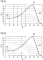
In einer bevorzugten Ausgestaltung weist die Strahlungsaustrittsfläche der optischen Vorrichtung einen konkav gekrümmten Teilbereich und einen den konkav gekrümmten Teilbereich zumindest teilweise umgebenden, konvex gekrümmten Teilbereich auf. Die optische Achse verläuft mit Vorzug durch den konkav gekrümmten Teilbereich und besonders bevorzugt gleichzeitig durch den Halbleiterchip, insbesondere im Wesentlichen durch dessen Zentrum, etwa den Schwerpunkt einer lateral verlaufenden Querschnittsfläche des Halbleiterchips. Strahlung, die im optoelektronischen Bauteil erzeugt wird und nicht deckungsgleich mit der optischen Achse direkt auf den konkav gekrümmten Teilbereich trifft, wird vorwiegend von der optischen Achse weg gebrochen.In a preferred embodiment, the radiation exit surface of the optical device has a concavely curved partial region and a convexly curved partial region surrounding the concavely curved partial region at least partially. The optical axis preferably passes through the concave curved portion, and more preferably at the same time through the semiconductor chip, in particular substantially through its center, such as the center of gravity of a laterally extending cross-sectional area of the semiconductor chip. Radiation generated in the optoelectronic device and not congruent with the optical axis directly on the concavely curved portion hits, is mainly refracted away from the optical axis.
So verringert sich der Anteil der Strahlung, welche sich im Wesentlichen in Richtung der optischen Achse, etwa unter einem Winkel von 20° oder weniger zur optischen Achse, ausbreitet. Dagegen erhöht sich der Strahlungsanteil, der die Beleuchtungsanordnung in großen Winkeln zur optischen Achse, beispielsweise 30° oder mehr, verlässt. Die von der Beleuchtungsanordnung abgestrahlte Strahlungsleistung als Funktion des Winkels zur optischen Achse zeigt vorzugsweise ein Maximum bei vergleichsweise großen Winkeln von 30° oder mehr, zum Beispiel bei einem Winkel zwischen einschließlich 60° und einschließlich 70°.Thus, the proportion of the radiation which propagates substantially in the direction of the optical axis, for example at an angle of 20 ° or less to the optical axis, is reduced. By contrast, the proportion of radiation which leaves the illumination arrangement at large angles to the optical axis, for example 30 ° or more, increases. The radiant power emitted by the illumination arrangement as a function of the angle to the optical axis preferably exhibits a maximum at comparatively large angles of 30 ° or more, for example at an angle of between 60 ° and 70 ° inclusive.
Eine Beleuchtungsanordnung mit einer solchen Abstrahlcharakteristik eignet sich besonders für die Ausleuchtung einer sich im Wesentlichen senkrecht zur optischen Achse der Beleuchtungsanordnung erstreckenden Fläche und insbesondere zur Hinterleuchtung von Anzeigevorrichtungen, etwa LCDs (liquid crystal display). Typischerweise ist die auszuleuchtende Fläche erheblich größer als die Fläche des Halbleiterchips. Eine Abstrahlcharakteristik mit einem Maximum der abgestrahlten Strahlungsleistung bei einem großen Winkel zur optischen Achse, bevorzugt bei einem Winkel von 60° oder mehr, ist von Vorteil, da so Bereiche der auszuleuchtenden Fläche in vergleichsweise großem Abstand zur optischen Achse auch bei geringen Abständen der Fläche von der Beleuchtungsanordnung beleuchtet werden können. So kann etwa die Hinterleuchtungseinheit eines LCDs vorteilhaft besonders kompakt mit einer geringen Bautiefe gefertigt sein.An illumination arrangement with such a radiation characteristic is particularly suitable for illuminating a surface extending substantially perpendicular to the optical axis of the illumination arrangement and in particular for backlighting display devices, such as LCDs (liquid crystal display). Typically, the area to be illuminated is considerably larger than the area of the semiconductor chip. A radiation characteristic with a maximum of the radiated radiation power at a large angle to the optical axis, preferably at an angle of 60 ° or more, is advantageous, since so areas of the surface to be illuminated at a relatively large distance from the optical axis even at small distances of the surface of the lighting arrangement can be illuminated. For example, the backlighting unit of an LCD can advantageously be made particularly compact with a small overall depth.
Bevorzugt weist der konvex gekrümmte Teilbereich einen ersten Unterbereich und einen zweiten Unterbereich auf, wobei die Krümmung des ersten Unterbereichs kleiner als die Krümmung des zweiten Unterbereichs ist. Dabei kann der zweite Unterbereich in einem größeren Abstand zur optischen Achse angeordnet sein als der erste Unterbereich. Vorzugsweise nimmt die Krümmung des konvex gekrümmten Teilbereichs, insbesondere die Krümmung des zweiten Unterbereichs, mit wachsendem Abstand vom konkav gekrümmten Teilbereich zu. Eine mit dem Abstand kontinuierlich zunehmende Krümmung ist bevorzugt, aber nicht zwingend. Eine Zunahme der Krümmung kann bewirken, dass der Anteil von Strahlung, die unter einem großen Winkel zur optischen Achse austritt, vorteilhaft erhöht ist. Eine gleichmäßige Ausleuchtung von Teilflächen der zu beleuchtenden Fläche, die sich in vergleichsweise großem Abstand zur optischen Achse befinden, wird so gefördert.Preferably, the convexly curved subregion has a first subregion and a second subregion, wherein the curvature of the first subregion is smaller than the curvature of the second subregion. In this case, the second Subregion may be arranged at a greater distance from the optical axis than the first sub-area. The curvature of the convexly curved subarea, in particular the curvature of the second subarea, preferably increases with increasing distance from the concavely curved subarea. A continuously increasing curvature with the distance is preferred, but not mandatory. An increase in the curvature may cause the proportion of radiation that exits at a large angle to the optical axis to be advantageously increased. A uniform illumination of partial surfaces of the surface to be illuminated, which are located at a relatively large distance from the optical axis, is promoted.
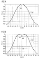
Strahlung, die aus der Oberfläche des Halbleiterchips austritt und direkt auf die Strahlungsaustrittsfläche trifft, wird von dieser besonders effizient in große Winkel von 30° und mehr zur optischen Achse gebrochen. Streustrahlung würde dagegen überwiegend in Richtung der optischen Achse gelenkt werden und in der Folge zu einer stärkeren Ausleuchtung der zu beleuchtenden Fläche im Bereich um deren Schnittpunkt mit der optischen Achse führen. Durch die gezielt absorbierende Ausbildung des reflektorartig geformten Elements kann dieser Streustrahlungsanteil vermindert werden. Eine auszuleuchtende Fläche kann so streustrahlungsarm, großflächig und besonders homogen ausgeleuchtet werden. Insbesondere kann das Ausbilden stärker ausgeleuchteter Bereiche, welche sich inselartig um den Schnittpunkt der Fläche mit der optischen Achse erstrecken, mit Vorteil vermindert werden.Radiation that emerges from the surface of the semiconductor chip and strikes directly on the radiation exit surface is refracted by it particularly efficiently into large angles of 30 ° and more to the optical axis. By contrast, scattered radiation would predominantly be directed in the direction of the optical axis and, as a consequence, lead to a greater illumination of the surface to be illuminated in the area around its point of intersection with the optical axis. Due to the targeted absorbing formation of the reflector-like shaped element of this scattered radiation component can be reduced. A surface to be illuminated can be illuminated in such a way as to be free from scattered radiation, over a large area and particularly homogeneously. In particular, the formation of more highly illuminated regions, which extend island-like around the intersection of the surface with the optical axis, can be advantageously reduced.
Weiterhin kann auch Strahlung, die von außerhalb der Beleuchtungsanordnung auf die Strahlungsaustrittsfläche trifft und durch die optische Vorrichtung hindurch tritt, einen Streustrahlungsanteil verursachen, falls diese Strahlung im Bauteil reflektiert wird und durch die Strahlungsaustrittsfläche der optischen Vorrichtung wieder austritt. Dieser wieder austretende Anteil der Strahlung wird auch als Phantomlicht bezeichnet und kann beim Einsatz der Beleuchtungsanordnung zur Hinterleuchtung von Anzeigevorrichtungen, wie beispielsweise LCDs oder LCD-Fernsehern, das Kontrastverhältnis der Anzeigevorrichtung mindern. Mit der gezielt absorbierenden Ausführung des reflektorartig geformten Elements und insbesondere des gesamten Gehäusekörpers kann der Phantomlichteinfluss weitgehend unterdrückt werden, was zu einer vorteilhaften Steigerung des Kontrastverhältnisses der Anzeigevorrichtung führen kann.Furthermore, radiation which strikes the radiation exit surface from outside the illumination arrangement and passes through the optical device may also cause a scattered radiation component if this radiation is reflected in the component and exits through the radiation exit surface of the optical device. This re-emerging portion of the radiation is also referred to as phantom light and can reduce the contrast ratio of the display device when using the illumination arrangement for the backlighting of display devices, such as LCDs or LCD TVs. With the targeted absorbent design of the reflector-like shaped element and in particular the entire housing body of the phantom light influence can be largely suppressed, which can lead to an advantageous increase in the contrast ratio of the display device.
In einer bevorzugten Ausgestaltung ist die optische Vorrichtung an dem optoelektronischen Bauteil befestigt. Dazu kann die optische Vorrichtung beispielsweise als Aufsatzoptik, insbesondere als Überstülpoptik, als Aufsteckoptik oder als Aufschnappoptik ausgeführt sein. Alternativ oder zusätzlich kann die optische Vorrichtung an das optoelektronische Bauteil geklebt werden.In a preferred embodiment, the optical device is attached to the optoelectronic component. For this purpose, the optical device can be designed, for example, as an attachment optics, in particular as a rollover optics, as a plug-on optics or as snap-on optics. Alternatively or additionally, the optical device can be glued to the optoelectronic component.
Hierbei ist unter einer Aufsteckoptik eine optische Vorrichtung zu verstehen, welche ein Befestigungselement aufweist, das in eine geeignete Montagevorrichtung des optoelektronischen Bauteils, z.B. eine Ausnehmung des Gehäusekörpers, eingesteckt werden kann. Ergänzend können die Befestigungselemente nach der Montage der optischen Vorrichtung an dem optoelektronischen Bauteil heißverstemmt werden, so dass die optische Vorrichtung besonders stabil und dauerhaft an dem optoelektronischen Bauteil befestigt ist.Here, a plug-in optical system is to be understood as an optical device which has a fastening element which can be inserted into a suitable mounting device of the optoelectronic component, e.g. a recess of the housing body, can be inserted. In addition, the fastening elements can be heat staked after the assembly of the optical device to the optoelectronic component, so that the optical device is particularly stable and permanently attached to the optoelectronic component.
Bei einer Aufschnappoptik weist die optische Vorrichtung ein Befestigungselement auf, welches in einer geeigneten Montagevorrichtung des optoelektronischen Bauteils einrastet.In a snap-on optical system, the optical device has a fastening element which engages in a suitable mounting device of the optoelectronic component.
Eine Überstülpoptik kann eingriffsfrei und/oder rastverbindungsfrei am optoelektronischen Bauteil befestigt werden. Spezielle Elemente zur Befestigung am optoelektronischen Bauteil sind bei einer Überstülpoptik nicht erforderlich. Ergänzend kann die Überstülpoptik an das optoelektronische Bauteil geklebt werden.
Bevorzugt ist die Beleuchtungsanordnung und insbesondere das optoelektronische Bauteil im Wesentlichen frei von Diffusoren und/oder Lumineszenzkonvertern ausgeführt, da sowohl Streuung von im optoelektronischen Bauteil erzeugter Strahlung an Diffusoren als auch die Absorption der Strahlung mit nachfolgender Re-Emission durch Lumineszenzkonverter dazu führen würde, dass die Abstrahlung des optoelektronischen Bauteils vermehrt ungerichtet erfolgen würde. Zudem ist die Umhüllung und gegebenenfalls die Zwischenschicht vorzugsweise klar ausgeführt. Dadurch kann die von dem optoelektronischen Bauteil zur Verfügung gestellte Strahlung durch die optische Vorrichtung vereinfacht gemäß einer vorgegebenen Abstrahlcharakteristik geformt werden. Gemäß der vorliegenden Erfindung ist das optoelektronische Bauteil als oberflächenmontierbares Bauteil (surface mountable device, SMD) ausgeführt.
Besonders bevorzugt ist die Beleuchtungsanordnung mit dem optoelektronischen Bauteil und an dem optoelektronischen Bauteil befestigten optischen Vorrichtung als Verbundbauteil ausgebildet. Als Verbundbauteil kann die Beleuchtungsanordnung als Ganzes vereinfacht, beispielsweise auf eine Leiterplatte, montiert werden. Vorzugsweise ist das Verbundbauteil als oberflächenmontierbares Bauteil ausgeführt.
Weitere Merkmale, vorteilhafte Ausgestaltungen und Zweckmäßigkeiten der Erfindung ergeben sich aus der folgenden Beschreibung der Ausführungsbeispiele in Verbindung mit den Figuren.
Es zeigen:
-
Figur 1 -
Figur 2 -
Figur 3 -
Figur 4 -
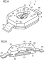
Figur 5A eine schematische perspektivische Ansicht einer erfindungsgemäßen Beleuchtungsanordnung, -
Figur 5B eine schematische Schnittansicht durch eine Beleuchtungsanordnung gemäßFigur 5A in perspektivischer Darstellung. -
Figur 6A ein Beispiel für die Abstrahlcharakteristik (relative Intensität I als Funktion des Winkels ϑ zur optischen Achse) einer Beleuchtungsanordnung mit einem nicht gezielt absorbierend ausgebildeten reflektorartig geformten Element, -
Figur 6B ein Beispiel für die Abstrahlcharakteristik (relative Intensität I als Funktion des Winkels ϑ zur optischen Achse) einer erfindungsgemäßen Beleuchtungsanordnung mit einem gezielt absorbierend ausgebildeten reflektorartig geformten Element, -
Figur 7A ein Beispiel für die relative Beleuchtungsstärke B als Funktion der Entfernung d zur optischen Achse für eine Beleuchtungsanordnung mit einem nicht gezielt absorbierend ausgebildeten reflektorartig geformten Element und -
Figur 7B ein Beispiel für die relative Beleuchtungsstärke B als Funktion der Entfernung d zur optischen Achse für eine erfindungsgemäße Beleuchtungsanordnung mit einem gezielt absorbierend ausgebildeten reflektorartig geformten Element.
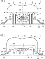
In
Weiterhin enthält das optoelektronische Bauteil einen zur Strahlungserzeugung vorgesehenen Halbleiterchip 5, der als Dünnfilm-Halbleiterchip ausgeführt ist. Ein typischer Aufbau eines Dünnfilm-Halbleiterchips ist im
Preferably, the illumination arrangement and in particular the optoelectronic component is designed substantially free of diffusers and / or luminescence converters, since both scattering of radiation generated in the optoelectronic component to diffusers and absorption of the radiation with subsequent re-emission by luminescence converters would lead to the Radiation of the optoelectronic device would be increasingly undirected. In addition, the sheath and optionally the intermediate layer is preferably made clear. As a result, the radiation provided by the optoelectronic component can be simplified by the optical device in accordance with a predetermined emission characteristic. According to the present invention, the optoelectronic device is designed as a surface mountable device (SMD).
Particularly preferably, the illumination arrangement with the optoelectronic component and optical device attached to the optoelectronic component is designed as a composite component. As a composite component, the lighting arrangement as a whole can be simplified, for example, mounted on a printed circuit board. Preferably, the composite component is designed as a surface mountable component.
Further features, advantageous embodiments and advantages of the invention will become apparent from the following description of the embodiments in conjunction with the figures.
Show it:
-
FIG. 1 a schematic sectional view of a first embodiment of a lighting arrangement according to the invention, -
FIG. 2 a schematic sectional view of a second embodiment of a lighting arrangement according to the invention, -
FIG. 3 an example of a schematic representation of the beam path in a lighting arrangement according to the invention, -
FIG. 4 a schematic sectional view of a particularly suitable for a lighting arrangement according to the invention semiconductor chip, -
FIG. 5A a schematic perspective view of a lighting arrangement according to the invention, -
FIG. 5B a schematic sectional view through a lighting arrangement according toFIG. 5A in perspective view. -
FIG. 6A an example of the radiation characteristic (relative intensity I as a function of the angle θ to the optical axis) of a lighting arrangement with a reflector-like shaped element which is not intentionally absorbed, -
FIG. 6B an example of the emission characteristic (relative intensity I as a function of the angle θ to the optical axis) of a lighting arrangement according to the invention with a reflector-like element formed in a specifically absorbing manner, -
FIG. 7A an example of the relative illuminance B as a function of the distance d to the optical axis for a Illumination arrangement with a not specifically absorbing formed reflector-like shaped element and -
FIG. 7B an example of the relative illuminance B as a function of the distance d to the optical axis for a lighting arrangement according to the invention with a reflector-like shaped element designed to be absorbent.
In the
Furthermore, the optoelectronic component contains a
The
The
Das reflektorartig geformte Element 3 ist für die im optoelektronischen Bauteil erzeugte Strahlung gezielt absorbierend ausgebildet. Dazu kann das reflektorartig geformte Element 3 und weitergehend der Gehäusekörper 20 vollständig oder teilweise aus einem die im optoelektronischen Bauteil erzeugte Strahlung absorbierenden Material oder einer absorbierenden Materialzusammensetzung gefertigt sein. Bevorzugt ist das reflektorartig geformte Element und insbesondere der Gehäusekörper schwarz oder dunkelgrau ausgeführt. Beispielsweise kann ein Gehäusekörper aus Kunststoff durch Zugabe von Farbstoffen, rußartigen oder rußähnlichen Partikeln in die verwendete Kunststoffmasse schwarz oder dunkelgrau ausgebildet sein.The reflector-like
Alternativ oder ergänzend kann das reflektorartig geformte Element 3 und insbesondere der Gehäusekörper 20 mit einem die im optoelektronischen Bauteil erzeugte Strahlung absorbierenden Material oder einer absorbierenden Materialzusammensetzung versehen, beispielsweise beschichtet, z.B. bedruckt oder bestempelt, sein.Alternatively or additionally, the reflector-like
Insbesondere beträgt die verbleibende Reflektivität des gezielt absorbierend ausgebildeten reflektorartig geformten Elements 3 im Wellenlängenbereich der vom optoelektronischen Bauteil emittierten Strahlung 15% oder weniger, bevorzugt 5% oder weniger.
Weiterhin ist der Halbleiterchip 5 auf einem ersten elektrischen Anschlussleiter 205 befestigt, der bevorzugt eine elektrisch leitende Verbindung zu einem externen Anschluss, z.B. einer Leiterbahn, ermöglicht. Ein zweiter elektrischer Anschlussleiter 206 kann beispielsweise über einen Bonddraht 290 mit der dem elektrischen Anschlussleiter abgewandten Oberseite 52 des Halbleiterchips elektrisch verbunden sein. Die Enden 207 des ersten 205 und zweiten 206 Anschlussleiters können mittels eines Lots 270, insbesondere eines bleifreien Lots, auf einer Leiterplatte 280 befestigt sein.
Der erste elektrischen Anschlussleiter 205 und der zweite elektrische Anschlussleiter 206 sind von dem Gehäusekörper 20 umformt und ragen aus verschiedenen Seiten des Gehäusekörpers heraus. Bevorzugt sind der erste und der zweite elektrische Anschlussleiter durch einen Leiterrahmen für das optoelektronische Bauteil 2 gebildet.
Weiterhin ist das optoelektronische Bauteil 2 als oberflächenmontierbares Bauteil ausgeführt. Die Beleuchtungsanordnung 1 kann mit dem optoelektronischen Bauteil 2 und der optischen Vorrichtung 4 als ein Verbundbauteil ausgeführt sein.
Gegenüber einer Einzelmontage des optoelektronischen Bauteils und der optischen Vorrichtung kann eine als oberflächenmontierbares Verbundbauteil ausgeführte Beleuchtungsanordnung vereinfacht auf der Leiterplatte 280 montiert werden.
Die Kavität 240 des Gehäusekörpers enthält eine Umhüllungsmasse 250, in welche der Halbleiterchip 5 und der Bonddraht eingebettet sind. Eine vollständige Einbettung ist hierbei von Vorteil. Diese Umhüllung dient zum Schutz des Halbleiterchips 5 und des Bonddrahts vor schädlichen äußeren Einflüssen und mechanischen Belastungen. Zweckmäßigerweise ist die Umhüllungsmasse strahlungsdurchlässig für vom Halbleiterchip erzeugte Strahlung ausgeführt.In particular, the remaining reflectivity of the targeted absorbing formed reflector-like
Furthermore, the
The first
Furthermore, the
Compared with a single assembly of the optoelectronic component and the optical device, a lighting assembly designed as a surface-mountable composite component can be mounted in a simplified manner on the printed
The
Weiterhin ist eine Zwischenschicht 260 zwischen der Umhüllungsmasse 250 und einer Strahlungseintrittsfläche 46 der optischen Vorrichtung 4 eingebracht, welche besonders bevorzugt an die Umhüllungsmasse und an die Strahlungseintrittsfläche unmittelbar angrenzt. Diese Zwischenschicht kann zur Brechungsindexanpassung zwischen der Umhüllung und der optischen Vorrichtung ausgebildet sein.Furthermore, an
Bevorzugt sind das optoelektronische Bauteil, die Zwischenschicht und die Umhüllung im Wesentlichen frei von Diffusoren und/oder Lumineszenzkonvertern ausgeführt. Dadurch kann eine vermehrt ungerichtete Abstrahlung vermieden werden, so dass die von dem optoelektronischen Bauteil zur Verfügung gestellte Strahlung durch die optische Vorrichtung vereinfacht gemäß einer vorgegebenen Abstrahlcharakteristik geformt werden kann.Preferably, the optoelectronic component, the intermediate layer and the cladding are designed essentially free of diffusers and / or luminescence converters. As a result, an increasingly non-directional radiation can be avoided, so that the radiation provided by the optoelectronic component can be simplified by the optical device in accordance with a predetermined radiation characteristic.
Eine optische Achse 40 der optischen Vorrichtung 4 verläuft durch den Halbleiterchip 5, insbesondere im Wesentlichen durch das Zentrum des Halbleiterchips. Bevorzugt ist die optische Achse senkrecht oder im Wesentlichen senkrecht zur Oberfläche 52 des Halbleiterchips 5. Die optische Vorrichtung weist ein Strahlformungsteil 48 und ein Trägerteil 49 auf. Das Trägerteil ist zur Befestigung der optischen Vorrichtung an dem optoelektronischen Bauteil vorgesehen;An
Das Strahlformungsteil 48 und das Trägerteil 49 der optischen Vorrichtung 4 können aus unterschiedlichen Materialien gefertigt und insbesondere aneinander angeformt sein. Durch das aneinander Anformen des Strahlformungsteils und des Trägerteils wird eine haftvermittlungsfreie mechanisch stabile Verbindung des Trägerteils mit dem Strahlformungsteil erleichtert. Die Materialien für das Trägerteil und das Strahlformungsteil können im Hinblick auf unterschiedliche Anforderungen ausgewählt werden. Bei dem Strahlformungsteil sind optische Eigenschaften wie Transparenz und Strahlungsresistenz für von dem optoelektronischen Bauteil emittierte Strahlung besonders bedeutsam.The
Bevorzugt enthält das Strahlformungsteil 48 ein Silikon oder ein Silikon-Hybridmaterial oder besteht aus einem derartigen Material. Das Trägerteil 49 ist dagegen nicht zur Strahlungsformung vorgesehen und kann deshalb auch strahlungsundurchlässig ausgebildet sein. Das Material für das Trägerteil kann hinsichtlich besonderer Anforderungen wie mechanische Stabilität oder gute Befestigungseigenschaften ausgewählt sein. Ein Thermoplast oder ein Duroplast ist für die Fertigung des Trägerteils besonders geeignet.The
Der Abstand zwischen der Strahlungseintrittsfläche 46 der optischen Vorrichtung und der Oberfläche des Halbleiterchips 52 beträgt 5 mm oder weniger, vorzugsweise 3mm oder weniger, bevorzugt 1 mm oder weniger, besonders bevorzugt etwa 0,6 mm. Die Beleuchtungsanordnung kann damit vorteilhaft besonders kompakt gefertigt sein.The distance between the
Während bei den in den
In
In
Die Zwischenschicht 260 füllt das Volumen zwischen der optischen Vorrichtung 4 und dem Gehäusekörper 20 zumindest teilweise aus. Das Volumen zwischen der Umhüllungsmasse 250 und der Strahlungseintrittsfläche 46 ist vorzugsweise vollständig mit der Zwischenschicht ausgefüllt. Weiterhin bevorzugt umgreift bei einer Überstülpoptik die Zwischenschicht den Gehäusekörper. Die Zwischenschicht kann ein Silikon, insbesondere ein Silikongel, oder ein Silikon-Hybridmaterial enthalten oder hieraus, bestehen. So kann die Zwischenschicht gleichzeitig die Funktion einer Brechungsindexanpassungsschicht erfüllen und der einfachen, stabilen und dauerhaften Befestigung der optischen Vorrichtung 4 am optoelektronischen Bauteil 2 dienen.The
Die in
Die Strahlungseintrittsfläche 46 ist im Wesentlichen eben ausgeführt. Die Strahlformung der im optoelektronischen Bauteil erzeugten Strahlung gemäß einer der Beleuchtungsanordnung vorgegebenen Beleuchtungsstärkeverteilung erfolgt bevorzugt vorwiegend an der Strahlungsaustrittsfläche, wodurch eine zuverlässige Strahlformung vereinfacht ermöglicht wird.The
Die Strahlungsaustrittsfläche 41 der optischen Vorrichtung ist vorzugsweise rotationssymmetrisch zur optischen Achse 40 der optischen Vorrichtung 4 ausgebildet. Teile der optischen Vorrichtung, die nicht der Strahlformung dienen, etwa das in den
Weiterhin weist die Strahlungsaustrittsfläche 41 einen konkav gekrümmten Teilbereich 42 auf. Die optische Achse 40 der optischen Vorrichtung 4 verläuft durch den konkav gekrümmten Teilbereich.Furthermore, the
Der konkav gekrümmte Teilbereich 42 ist von einem konvex gekrümmten Teilbereich 43, insbesondere vollständig, umgeben. Bevorzugt ist der Flächeninhalt des konvex gekrümmten Teilbereichs größer als der Flächeninhalt des konkav gekrümmten Teilbereichs. Weiterhin weist der konvex gekrümmte Teilbereich einen ersten konvex gekrümmten Unterbereich 44 und einen zweiten konvex gekrümmten Unterbereich 45 auf.The concave
Die im aktiven Bereich 51 des Halbleiterchips 5 erzeugte Strahlung tritt durch eine Oberfläche 52 des Halbleiterchips und eine Seitenfläche 53 aus. Die Wirkung der optischen Vorrichtung 4 auf aus der Oberfläche austretende Strahlung ist beispielhaft anhand der Strahlen 60, 61 und 62 gezeigt.The radiation generated in the
Für Strahlung 60, die auf den konkav gekrümmten Teilbereich 42 der Strahlungsaustrittsfläche 41 trifft, wirkt die optische Vorrichtung wie eine Zerstreuungslinse. Deshalb wird Strahlung, die schräg zur optischen Achse 40 oder in einem von null verschiedenen Abstand parallel zur optischen Achse auf den konkav gekrümmten Bereich der Strahlungsaustrittsfläche trifft, von der optischen Achse weg gebrochen. Dadurch verringert sich vorteilhaft der Strahlungsanteil, welcher die zu beleuchtende Fläche 80 im Bereich nahe der optischen Achse trifft. Ebenso wird Strahlung 61 und 62, welche auf den ersten 44 bzw. zweiten 45 konvex gekrümmten Unterbereich trifft, von der optischen Achse weg gebrochen. Der zweite konvex gekrümmte Unterbereich 45 ist bevorzugt stärker gekrümmt als der erste konvex gekrümmte Unterbereich 44, da so auf den zweiten Unterbereich auftreffende Strahlung 62 besonders effizient in große Winkel zur optischen Achse gebrochen werden kann.For
Bevorzugt ist die Strahlungsaustrittsfläche 41 ohne kantige Übergänge ausgeführt, d.h. die gesamte Strahlungsaustrittsfläche ist eine an jedem Punkt, insbesondere an einem Übergang 47 zwischen dem konkav gekrümmten Teilbereich 42 und dem konvex gekrümmten Teilbereich 43, differenzierbare Fläche. Durch kantige Übergänge verursachte hellere oder dunklere Bereiche wie beispielsweise Ringe höherer Intensität auf der auszuleuchtenden Fläche können so mit Vorteil vermieden werden. Zudem verlaufen die Strahlengänge in bzw. an der optischen Vorrichtung bevorzugt im Wesentlichen totalreflexionsfrei.Preferably, the
Weiterhin ist die optische Vorrichtung bevorzugt so ausgeführt, dass sich zwei beliebige Strahlen, die von dem Bereich des aktiven Bereichs 51 ausgehen, der von der optischen Achse durchdrungen wird, nach dem Austritt aus der Strahlungsaustrittsfläche 41 nicht überschneiden. Sich überschneidende Strahlen können den Effekt einer lokalen Bündelung von Strahlung haben, so dass sich auf der zu beleuchtenden Fläche 80 zur Beleuchtungsanordnung Inhomogenitäten in der Bestrahlungsstärke, etwa in Form von Ringen oder Kreisen höherer Intensität, ausbilden können. Für den Fall einer idealen Punktlichtquelle, die auf der optischen Achse angeordnet ist, kann so eine solche lokale Bündelung vollständig vermieden werden.Furthermore, the optical device is preferably designed so that any two rays which emanate from the region of the
Insbesondere Strahlung, die vor dem Auftreffen auf die Strahlungsaustrittsfläche 41 der optischen Vorrichtung 4 eine Reflexion erfährt, kann, sich überkreuzende Strahlengänge verursachen. Dies ist durch die in
Für die Strahlen 70 ist durch Pfeile mit gestrichelten Linien 71 und 72 angedeutet, wie die Strahlen nach einer Reflexion an dem reflektorartig geformten Element verlaufen würden, wenn das reflektorartig geformte Element 3 nicht wie im Zusammenhang mit
Außerdem würden im Falle einer gerichteten Reflexion an dem reflektorartig geformten Element sowohl der Strahl 71, welcher auf den konkav gekrümmten Teilbereich 42 der Strahlungsaustrittsfläche 41 umgelenkt würde, als auch der Strahl 72, welcher auf den konvex gekrümmten Teilbereich 43 treffen würde, nicht von der optischen Achse weg gebrochen werden, sondern vorwiegend zu einer Ausleuchtung des Teilbereichs der auszuleuchtenden Fläche 80 nahe der optischen Achse führen. Dieser zentrale Bereich der Fläche wäre dadurch stärker ausgeleuchtet. Auch ein reflektorartig geformtes Element, das diffus reflektierend mit einem hohen Reflexionskoeffizienten ausgeführt ist, etwa ein reflektorartig geformtes Element, das durch eine weiße Kunststoffoberfläche gebildet ist, würde vermehrt einen. Streulichtanteil verursachen und folglich eine stärkere Ausleuchtung der zu beleuchtenden Fläche im Bereich nahe des Schnittpunkts mit der optischen Achse, etwa in einem Abstand von 10 mm oder weniger zur optischen Achse, bewirken. Aufgrund der gezielt absorbierenden Ausführung des reflektorartig geformten Elements kann eine besonders homogene Ausleuchtung einer zu beleuchtenden Fläche, etwa einer Anzeigevorrichtung wie einem LCD, erzielt werden.In addition, in the case of a directed reflection on the reflector-like shaped element, both the
Bei einer Beleuchtungsanordnung, die zur Hinterleuchtung einer Anzeigevorrichtung vorgesehen ist, ist der Gehäusekörper vorzugsweise vollständig für den gesamten sichtbaren Spektralbereich gezielt absorbierend ausgebildet. Eine inhomogene Ausleuchtung infolge von Phantomstrahlung kann so besonders stark vermindert werden.In a lighting arrangement which is provided for the backlighting of a display device, the housing body is preferably designed to be completely absorbent for the entire visible spectral range. Inhomogeneous illumination due to phantom radiation can thus be greatly reduced.
Die weitgehende Reduktion des Streulichtanteils erleichtert generell die Strahlformung der im optoelektronischen Bauteil erzeugten Strahlung gemäß einer der Beleuchtungsanordnung vorgegebenen, insbesondere gerichteten, Abstrahlcharakteristik.The substantial reduction of the scattered light component generally facilitates the beam shaping of the radiation generated in the optoelectronic component in accordance with a radiation characteristic predetermined, in particular directed, of the illumination arrangement.
In
Der Halbleiterchip 5 weist einen auf einem Träger 55 angeordneten Halbleiterkörper 54 auf. Der Halbleiterkörper umfasst eine Halbleiterschichtenfolge mit einem zur Strahlungserzeugung vorgesehenen aktiven Bereich 51. Die Halbleiterschichtenfolge bildet den Halbleiterkörper 54. Auf der dem Träger abgewandten Seite des Halbleiterkörpers ist ein erster Kontakt 58 angeordnet, über den der Halbleiterchip in Verbindung mit einem auf der dem Halbleiterkörper abgewandten Seite des Trägers angeordneten zweiten Kontakt 59 elektrisch anschließbar ist. Der erste Kontakt 58 ist insbesondere zur elektrisch leitenden Verbindung mit einem Bonddraht und der zweiten Kontakt 59 zur elektrisch leitenden Verbindung mit einem Anschlussleiter vorgesehen. Die Kontakte können beispielsweise jeweils ein Metall oder eine Legierung enthalten.The
In einer bevorzugten Ausgestaltung enthält der Halbleiterkörper 54, insbesondere der aktive Bereich 51, mindestens ein III-V-Halbleitermaterial, etwa ein Material aus den Materialsystemen InxGayAl1-x-yP, InxGayAl1-x-yN oder InxGayAl1-x-yAs, jeweils mit 0≤x≤1, 0≤y≤1 und x+y≤1, insbesondere mit x ≠ 0, y ≠ 0, x ≠ 1 und/oder y ≠ 1. Bevorzugt erfolgt die Herstellung der Halbleiterschichtenfolge in einem, insbesondere epitaktischen, Abscheideprozess, etwa mittels MBE oder MOVPE auf einem Aufwachssubstrat.In a preferred embodiment, the
III-V-Halbleitermaterialien sind zur Strahlungserzeugung im ultravioletten (InxGayAl1-x-yN) über den sichtbaren (InxGayAl1-x-yN, insbesondere für blaue bis grüne Strahlung, oder InxGayAl1-x-yP, insbesondere für gelbe bis rote Strahlung) bis in den infraroten (InxGayAl1-x-yAs) Spektralbereich besonders geeignet. Mit III-V-Halbleitermaterialien, insbesondere aus den genannten Materialsystemen, können weiterhin bei der Strahlungserzeugung vorteilhaft hohe interne Quanteneffizienzen erzielt werden.III-V semiconductor materials are used for generating radiation in the ultraviolet (In x Ga y Al 1-xy N) over the visible (In x Ga y Al 1-xy N, in particular for blue to green radiation, or In x Ga y Al 1- xy P, in particular for yellow to red radiation) to the infrared (In x Ga y Al 1-xy As) spectral range is particularly suitable. With III-V semiconductor materials, in particular from the mentioned material systems, it is furthermore possible to achieve advantageously high internal quantum efficiencies in the generation of radiation.
In einer weiteren bevorzugten Ausgestaltung umfasst der aktive Bereich 51 eine Heterostruktur, insbesondere eine Doppelheterostruktur. Weiterhin kann die aktive Zone eine Einfach- oder eine Mehrfach-Quantentopfstruktur umfassen. Mittels derartiger Strukturen, insbesondere einer Mehrfach-Quantentopfstruktur oder einer Doppelheterostruktur, können besonders hohe interne Quanteneffizienzen erzielt werden.In a further preferred embodiment, the
Die Bezeichnung Quantentopfstruktur umfasst im Rahmen der Anmeldung jegliche Struktur, bei der Ladungsträger durch Einschluss ("confinement") eine Quantisierung ihrer Energiezustände erfahren oder erfahren können. Insbesondere beinhaltet die Bezeichnung Quantentopfstruktur keine Angabe über die Dimensionalität der Quantisierung. Sie umfasst somit unter anderem Quantentröge, Quantendrähte und Quantenpunkte und jede Kombination dieser Strukturen.Within the scope of the application, the term quantum well structure encompasses any structure in which charge carriers can experience or experience quantization of their energy states by confinement. In particular, the term quantum well structure does not include information about the dimensionality of the quantization. It thus includes quantum wells, quantum wires and quantum dots and any combination of these structures.
In einer weiteren bevorzugten Ausgestaltung ist auf dem Halbleiterkörper eine Spiegelschicht 56 angeordnet. Besonders bevorzugt ist die Spiegelschicht zwischen dem Halbleiterkörper 54 und dem Träger 55 angeordnet. Die Spiegelschicht kann beispielsweise als metallhaltige, insbesondere im Wesentlichen metallische, Spiegelschicht ausgeführt sein. Im aktiven Bereich erzeugte Strahlung kann an der Spiegelschicht reflektiert werden, wodurch einer Absorption in den der Spiegelschicht vom aktiven Bereich aus gesehen nachgeordneten Strukturen, etwa dem Träger, vorgebeugt wird. Die Effizienz des Halbleiterchips 5 kann so erhöht werden. Beispielsweise enthält die Spiegelschicht Au, Al, Ag, Pd, Rh, Pt oder eine Legierung mit mindestens einem dieser-Materialien. Al, Pd, Rh und Ag weisen im ultravioletten und blauen Spektralbereich, Au auch im gelben, orangen und roten bis in den infraroten Spektralbereich besonders hohe Reflektivitäten auf. Weiterhin wird durch Reflexion an der Spiegelschicht der Anteil an der der Spiegelschicht 56 gegenüberliegenden Seite des Halbleiterkörpers austretenden Strahlung erhöht.In a further preferred refinement, a
Zwischen dem Träger 55 und der Spiegelschicht 56 kann eine Verbindungsschicht 57 angeordnet sein, mittels derer der Halbleiterkörper seitens der Spiegelschicht auf dem Träger befestigt ist. Die Verbindungsschicht 307 kann beispielsweise als Lotschicht ausgeführt sein.Between the
Der in
Mit Vorteil muss der Träger im Gegensatz zu dem Aufwachssubstrat nicht die hohen Anforderungen hinsichtlich der kristallinen Reinheit erfüllen, sondern kann vielmehr im Hinblick auf andere Kriterien, wie beispielsweise mechanische Stabilität, thermische oder elektrische Eigenschaften ausgewählt werden.Advantageously, unlike the growth substrate, the support does not have to meet the stringent crystalline purity requirements, but rather may be selected for other criteria such as mechanical stability, thermal or electrical properties.
Bevorzugt weist der Träger 55 eine vergleichsweise hohe Wärmeleitfähigkeit auf. Beispielsweise enthält der Träger Ge. Auch ein GaAs-haltiger Träger kann Anwendung, finden.Preferably, the
Der aktive Bereich 51 ist bevorzugt mit dem zweiten Kontakt 59 über den elektrisch leitfähigen Träger, die elektrisch leitfähige Verbindungsschicht und die elektrisch leitfähige Spiegelschicht sowie die Halbleiterschichtenfolge des Halbleiterkörpers elektrisch leitend verbunden.The
Enthält der Träger ein Halbleitermaterial, so ist der Träger vorzugsweise zur Erhöhung der Leitfähigkeit geeignet dotiert.If the carrier contains a semiconductor material, the carrier is preferably suitably doped to increase the conductivity.
Zur Herstellung eines Dünnfilm-Halbleiterchips wird beispielsweise zunächst die Halbleiterschichtenfolge des Halbleiterkörpers 54 auf dem Aufwachssubstrat hergestellt. Die Halbleiterschichtenfolge bildet den Halbleiterkörper 54. Nachfolgend wird auf die dem Aufwachssubstrat abgewandte Seite des vorgefertigten Halbleiterkörpers die Spiegelschicht 56, etwa mittels Aufdampfens oder Sputterns, aufgebracht. Seitens der Spiegelschicht wird der Verbund mit Halbleiterschichtenfolge und Aufwachssubstrat hierauf über die Verbindungsschicht 57 mit dem Träger 55 verbunden, woraufhin das Aufwachssubstrat, etwa mittels Ätzens oder Lasertrennens, entfernt oder abgelöst wird.
Ein Dünnfilm-Halbleiterchip, etwa ein Dünnfilm-Leuchtdioden-Chip, kann sich weiterhin im Rahmen der vorliegenden Erfindung durch folgende charakteristische Merkmale auszeichnen:
- an einer zu einem Trägerelement, z.B.
dem Träger 55, hin gewandten ersten Hauptfläche eines Halbleiterkörpers, der eine Halbleiterschichtenfolge mit einem aktiven Bereich umfasst, insbesondere einer Epitaxieschichtenfolge, ist eine Spiegelschicht aufgebracht oder, etwa als Braggspiegel in der Halbleiterschichtenfolge integriert, ausgebildet, die zumindest einen Teil der in der Halbleiterschichtenfolge erzeugten Strahlung in diese zurückreflektiert; - die Halbleiterschichtenfolge weist eine Dicke im Bereich von 20µm oder weniger, insbesondere
im Bereich von 10 µm auf; und/oder - die Halbleiterschichtenfolge enthält mindestens eine Halbleiterschicht mit zumindest einer Fläche, die eine Durchmischungsstruktur aufweist, die im Idealfall zu einer annähernd ergodischen Verteilung des Lichtes in der Halbleiterschichtenfolge führt, d.h. sie weist ein möglichst ergodisch stochastisches Streuverhalten auf.
A thin-film semiconductor chip, for example a thin-film light-emitting diode chip, can furthermore be characterized in the context of the present invention by the following characteristic features:
- On a first main surface of a semiconductor body facing a carrier element, eg the
carrier 55, which comprises a semiconductor layer sequence with an active region, in particular an epitaxial layer sequence, a mirror layer is applied or, for example integrated as a Bragg mirror in the semiconductor layer sequence, which forms at least one Reflects part of the radiation generated in the semiconductor layer sequence in this back; - the semiconductor layer sequence has a thickness in the range of 20 μm or less, in particular in the range of 10 μm ; and or
- The semiconductor layer sequence contains at least one semiconductor layer with at least one surface which has a mixed-through structure which, in the ideal case, leads to an approximately ergodic distribution of the light in the semiconductor layer sequence, ie it has a possibly ergodically stochastic scattering behavior.
Die der Spiegelschicht abgewandte Oberfläche 52 des Halbleiterkörpers ist bei dem dargestellten Dünnfilmchip als eine Hauptstrahlungsauskoppelfläche ausgebildet. Eine Seitenfläche 53 bildet eine Nebenstrahlungsaustrittsfläche. Die aus der Hauptstrahlungsauskoppelfläche austretende Strahlungsleistung ist dabei größer als die aus der Nebenstrahlungsaustrittsfläche austretende Strahlungsleistung. Insbesondere ist die Summe der aus den Nebenstrahlungsaustrittsflächen austretenden Strahlungsleistung kleiner als die durch die Hauptstrahlungsauskoppelfläche austretende Strahlungsleistung.The
In Dünnfilm-Halbleiterchips verringert sich die aus den seitlichen Nebenstrahlungsaustrittsflächen austretende Strahlungsleistung zugunsten einer gesteigerten aus der Hauptstrahlungsauskoppelfläche ausgekoppelten Strahlungsleistung. Da von der Beleuchtungsanordnung 1 bevorzugt im Wesentlichen nur die aus der Oberfläche 52 des Halbleiterchips austretende Strahlung zur Verfügung gestellt werden soll, während seitlich austretende Strahlung wie im Zusammenhang mit
Es sei angemerkt, dass eine andere Beleuchtungsanordnung, die nicht gemäß der vorliegenden Erfindung ausgeführt ist, selbstverständlich nicht nur mit einem Dünnfilm-Halbleiterchip realisiert werden kann. Auch ein Halbleiterchip, bei dem das Aufwachssubstrat nicht abgelöst ist, kann für die Beleuchtungsanordnung geeignet sein. Ein solcher Halbleiterchip kann den in
Ein weiteres Ausführungsbeispiel einer Beleuchtungsanordnung ist in den
Die Kavität 240 ist als Ausnehmung in einer ersten Hauptfläche 202 des Gehäusekörpers 20 gebildet. Ein Boden 241 der Kavität verläuft vorzugsweise im Wesentlichen parallel zur ersten Hauptfläche. Bevorzugt nimmt die Ausdehnung der Kavität in einer sich parallel zur ersten Hauptfläche erstreckenden Ebene mit zunehmendem Abstand von der ersten Hauptfläche, insbesondere kontinuierlich, ab, so dass der Boden der Kavität einen kleineren Durchmesser aufweist als der Durchmesser der Kavität in der Ebene der ersten Hauptfläche. Beispielsweise kann die Kavität im Wesentlichen die Form eines Kegelstumpfs, dessen Durchmesser mit zunehmendem Abstand von der ersten Hauptfläche abnimmt, aufweisen.It should be noted that, of course, another lighting device not according to the present invention can be realized not only with a thin film semiconductor chip. Also, a semiconductor chip, in which the growth substrate is not detached, may be suitable for the lighting arrangement. Such a semiconductor chip can be used in
Another embodiment of a lighting arrangement is in the
The
An dem optoelektronischen Bauteil kann eine vom optoelektronischen Bauteil separate Optik befestigt, etwa aufgesteckt oder angeklebt, sein. Diese ist aus Gründen der Übersichtlichkeit nicht gezeigt.On the optoelectronic component, a separate from the optoelectronic device optics attached, such as plugged or glued be. This is not shown for reasons of clarity.
Im Unterschied zum optoelektronischen Bauteil gemäß den
Das thermische Anschlussteil 215 ist beispielsweise in eine Lasche eines ersten Anschlussleiters 205 eingelegt, eingesteckt oder anderweitig mit dem ersten Anschlussleiter, insbesondere elektrisch leitend und/oder mechanisch, lateral umfangsseitig verbunden. Weiterhin weist die erste Hauptfläche 202 des Gehäusekörpers 20 eine Ausnehmung 213, welche in der Wand 245 der Kavität gebildet ist, auf. Diese Ausnehmung ist für eine elektrisch leitende Verbindung eines zweiten elektrischen Anschlussleiters 206 mit dem Halbleiterchip 5, beispielsweise mittels des Bonddrahts 290, vorgesehen. Der zweite Anschlussleiter 206 ist vorzugsweise bezüglich der Chipmontage-Ebene des Halbleiterchips 5 auf dem thermischen Anschlussteil 215 erhöht. Das thermische Anschlussteil kann ferner seitens der zweiten Hauptfläche 204 aus dem Gehäusekörper herausragen oder im Wesentlichen eben mit dem Gehäusekörper abschließen. Beispielsweise enthält das thermische Anschlussteil ein Metall hoher Wärmeleitfähigkeit, etwa Cu oder Al, oder eine Legierung, etwa eine CuW-Legierung. Ein Leiterrahmen mit einem derartig ausgebildeten Anschlussteil und einem.Gehäusekörper ist in der
In den
In the
Die zweite Beleuchtungsanordnung ist wie im Zusammenhang mit den
Der Gehäusekörper 20 der ersten Beleuchtungsanordnung ist aus hochreflektierendem Kunststoff gefertigt, wobei durch Zugabe von TiO2-Partikeln in die Kunststoffmasse Reflektivitäten von etwa 85% für die Oberfläche des Gehäusekörpers und damit für das reflektorartig geformte Element erreicht werden. Bei der zweiten Beleuchtungsanordnung ist dagegen der Gehäusekörper und somit das reflektorartig geformte Element dadurch gezielt absorbierend ausgebildet, dass die Kunststoffmasse, aus welcher der Gehäusekörper gefertigt ist, durch Zugabe von rußartigen Partikeln schwarz gefärbt ist, so dass die Reflektivität des Gehäusekörpers im sichtbaren Spektralbereich etwa 5% beträgt.The
Eine.Kurve 400 zeigt, den Verlauf der Intensität der von der ersten Beleuchtungsanordnung abgestrahlten optischen Leistung in Abhängigkeit vom Winkel zur optischen Achse. Dabei ist die Intensität auf 1 normiert und somit als relative Intensität angegeben.A
Entsprechend zeigt eine Kurve 450 die Abstrahlcharakteristik der zweiten Beleuchtungsanordnung, wobei die Intensitätskurve wiederum normiert ist.Accordingly, a
Sowohl die Kurve 400 als auch die Kurve 450 weisen bei einem Winkel von etwa 67° zur optischen Achse ein globales Maximum 410 bzw. 460 der Intensität auf. Demnach bewirkt die beschriebene optische Vorrichtung, dass die im optoelektronischen Bauteil erzeugte Strahlung überwiegend nicht entlang der optischen Achse abgestrahlt wird.Both the
Da sich die erste und die zweite Beleuchtungsanordnung im Wesentlichen lediglich durch die Ausführung des reflektorartig geformten Elements unterscheiden, erfährt Strahlung, welche durch die jeweilige Hauptstrahlungsauskoppelfläche 52 austritt und direkt auf die Strahlungsaustrittsfläche trifft, bei beiden Beleuchtungsanordnungen eine im Wesentlichen gleiche Strahlungsformung. Unterschiede zwischen der Abstrahlungscharakteristik der ersten und der zweiten Beleuchtungsanordnung ergeben sich deshalb vorwiegend aufgrund von Strahlung, die den Halbleiterchip jeweils durch eine Seitenfläche 53 verlässt.Since the first and the second illumination arrangement essentially differ only by the embodiment of the reflector-like shaped element, radiation which emerges through the respective main radiation coupling-
Bei der ersten Beleuchtungsanordnung ist das reflektorartig geformte Element 3 aufgrund seiner Formgebung und Anordnung relativ zum Strahlung erzeugenden Halbleiterchip geeignet, zumindest einen Teil der auf das reflektorartig geformte Element treffenden Strahlung auf die Strahlungsaustrittsfläche 41 umzulenken. Wegen der vergleichsweise hohen Reflektivität von etwa 85% kann deshalb ein beträchtlicher Teil der aus den Seitenflächen 53 austretenden Strahlung auf die Strahlungsaustrittsfläche 41 der optischen Vorrichtung 4 umgelenkt werden.In the case of the first illumination arrangement, the reflector-like-shaped
Bei der zweiten Beleuchtungsanordnung ist das reflektorartig geformte Element dagegen für die im Halbleiterchip erzeugte Strahlung gezielt absorbierend ausgebildet, so dass das reflektorartig geformte Element aufgrund der geringen Reflektivität von etwa 5% trotz seiner Form und Anordnung nur einen erheblich geringeren Teil der aus einer der Seitenflächen 53 austretenden Strahlung auf die Strahlungsaustrittsfläche umlenkt.In contrast, in the second illumination arrangement, the reflector-like shaped element is specifically designed to absorb the radiation generated in the semiconductor chip so that the reflector-like shaped element, due to the low reflectivity of about 5%, despite its shape and arrangement, only a significantly smaller portion of one of the side surfaces 53 Exiting radiation deflects to the radiation exit surface.
Im Bereich großer Winkel zur optischen Achse, etwa zwischen 45° und 90°, zeigen die beiden Kurven 400 und 450 einen sehr ähnlichen Verlauf. Von der Beleuchtungsanordnung in diesen Winkelbereich ausgesendete Strahlung ist vorwiegend der Strahlungsanteil, welcher aus der Hauptstrahlungsauskoppelfläche des jeweiligen Halbleiterchips ausgekoppelt wurde.In the region of large angles to the optical axis, approximately between 45 ° and 90 °, the two
Für kleinere Winkel zur optischen Achse, von 0° bis etwa 45°, ist die relative Intensität 400 der von der ersten Beleuchtungsanordnung emittierten Strahlung 420, insbesondere im Winkelbereich von 0° bis etwa 30°, signifikant höher als die relative Intensität der von der zweiten Beleuchtungsanordnung in den entsprechenden Bereich 430 emittierte Strahlung. Dies wird, wie im Zusammenhang mit
Eine Abstrahlungscharakteristik mit einem Maximum bei Winkeln von 60° oder größer bei gleichzeitiger zusätzlicher Reduktion der in kleine Winkel zur optischen Achse 40 abgestrahlten Strahlungsleistung kann demnach durch die gezielt absorbierende Ausführung des reflektorartig geformten Elements verbessert erzielt werden.A radiation characteristic with a maximum at angles of 60 ° or greater with simultaneous additional reduction of radiated into small angles to the
Die Messungen der in den
Da die Strahlungsaustrittsfläche der optischen Vorrichtung rotationssymmetrisch zur optischen Achse ausgebildet, ist, und die optische Achse im Wesentlichen durch das Zentrum des Halbleiterchips verläuft, sind die beiden Beleuchtungsstärkeverteilungen 500 und 550 im Wesentlichen symmetrisch zur y-Achse.Since the radiation exit surface of the optical device is rotationally symmetrical with respect to the optical axis, and the optical axis extends essentially through the center of the semiconductor chip, the two
Im Bereich nahe der y-Achse, etwa für |d|≤10mm, unterscheidet sich der Verlauf 560 der Beleuchtungsstärke bei der zweiten Beleuchtungsanordnung deutlich von dem Verlauf 510 bei der ersten Beleuchtungsanordnung. Während bei der Kurve 500 die Beleuchtungsstärke bei d=10 mm um etwa 5% gegenüber dem Maximalwert abgefallen ist, beträgt der entsprechende Abfall bei der zweiten Kurve lediglich etwa 1%.In the region near the y-axis, for example for | d | ≦ 10 mm, the
Bei der ersten Beleuchtungsanordnung kann aus den Seitenflächen austretende Strahlung vom reflektorartig geformten Element hoher Reflektivität auf die Strahlungsaustrittsfläche 41 umgelenkt werden. Dieser Strahlungsanteil trifft unter einem nur schwer zu kontrollierenden Winkel auf die Strahlungsaustrittsfläche und kann deshalb von der optischen Vorrichtung 4 nur schwer gemäß der der Beleuchtungsanordnung vorgegebenen Abstrahlcharakteristik geformt werden. Die Ablenkung erfolgt überwiegend in vergleichsweise kleine Winkel zur optischen Achse, was zu einer im Bereich 510 überhöhten Beleuchtungsstärke führt. Bei der zweiten Beleuchtungsanordnung dagegen ist das reflektorartig geformte Element gezielt absorbierend ausgebildet, so dass aus der Seitenfläche 53 des Halbleiterchips austretende Strahlung vorwiegend absorbiert wird. Die gesamte der optischen Vorrichtung zur Verfügung gestellte Strahlungsleistung lässt sich dadurch verbessert gemäß einer vorgegebenen Beleuchtungsstärkeverteilung formen.. Wie durch einen Pfeil 561 angedeutet, bewirkt dies im Bereich 560 die gewünschte Reduktion der Beleuchtungsstärke und einen langsameren Abfall der Beleuchtungsstärke mit zunehmendem Abstand zur optischen Achse. Beispielsweise beträgt der Abfall der relativen Beleuchtungsstärke bei d=30mm etwa 0.32 für die Kurve 500, aber nur 0.22 für die Kurve 550.In the first illumination arrangement, radiation emerging from the side surfaces can be deflected by the reflector-like element of high reflectivity onto the
Eine gebräuchliche Kenngröße für die Breite einer Verteilung ist die volle Halbwertsbreite, welche angibt, wie breit der Bereich um das Maximum der Verteilung ist, im dem der Funktionswert der Verteilung 50% oder mehr des maximalen Funktionswerts beträgt. In
Die in
Zudem kann eine solche Beleuchtungsanordnung beispielsweise für die Allgemeinbeleuchtung, die Effektbeleuchtung, die Ausleuchtung von Leuchtreklamen oder für Leuchtbuchstaben (channel letters) eingesetzt werden.In addition, such a lighting arrangement can be used, for example, for general lighting, effect lighting, illumination of neon signs or for channel letters.
Die Erfindung ist in Anspruch 1 definiert und nicht durch die Beschreibung anhand der Ausführungsbeispiele beschränkt.The invention is defined in
Claims (15)
- Lighting arrangement (1), comprising an optical apparatus (4) with a radiation outlet surface (41) and an optoelectronic component (2) for producing radiation, wherein- an element (3) which is formed like a reflector being formed, whose shape and arrangement are suitable for deflecting radiation generated in the component through the radiation outlet surface,- the optoelectronic component (2) is formed as a surface-mountable SMD-component, and- the element (3) which is formed like a reflector being designed to specifically absorb radiation which is generated in the component, wherein- the optoelectronic component (2) comprises the element which is formed like a reflector and which is designed specifically absorbent, and- the optoelectronic component (2) comprises at least one semiconductor chip (5) which is suitable for radiation production,characterised in that
the reflectivity of the element (3) which is formed like a reflector is less than or equal to 15%, and
the semiconductor chip is formed as a thin-film semiconductor chip, with the semiconductor body being arranged on a carrier and with the carrier being different from a growth substrate. - Lighting arrangement according to claim 1, in which the radiation outlet surface (41) has a concave-curved subarea (42) and a convex-curved subarea (43) which at least partially surrounds the concave-curved subarea.
- Lighting arrangement according to claim 1 or 2, in which the optical apparatus (4) is attached to the optoelectronic component (2).
- Lighting arrangement according to one of the preceding claims, in which a minimum distance between the radiation outlet surface (41) and the semiconductor chip (5) is less than or equal to 5 mm.
- Lighting arrangement according to one of the preceding claims, in which a minimum distance between the radiation outlet surface (41) and the semiconductor chip (5) is less than or equal to 3 mm.
- Lighting arrangement according to one of the preceding claims, in which the optical apparatus (4) is designed to form an emission characteristic which is predetermined for the lighting arrangement, with radiation which is output from the semiconductor chip (5) being at least partially prevented from striking the radiation outlet surface (41) after reflection within the lighting arrangement.
- Lighting arrangement according to one of the preceding claims, in which a surface of the semiconductor chip (5) forms a main radiation output surface (52), and a side surface forms a secondary radiation outlet surface (53), wherein the shape and arrangement of the element (3) which is formed like a reflector are suitable for deflecting at least a part of the radiation which emerges from the secondary radiation outlet surface.
- Lighting arrangement according to one of the preceding claims, in which the semiconductor chip (5) comprises a semiconductor body (54), which comprises a semiconductor layer sequence with an active area (51) which is intended to generate radiation, and a carrier (55), with the semiconductor body being arranged on the carrier and with the carrier being different from a growth substrate of the semiconductor layer sequence.
- Lighting arrangement according to claim 8, in which a mirror layer (56) is arranged between the semiconductor body (54) and the carrier (55), where the mirror layer (56) comprises a metal or is metallic.
- Lighting arrangement according to one of the claims 1 to 9, in which the optoelectronic component comprises a housing body (20) and an external electrical connecting conductor (205), with the housing body containing the element (3) which is formed like a reflector, and with the semiconductor chip (5) being mounted on the connecting conductor.
- Lighting arrangement according to claim 10, in which the element (3) which is formed like a reflector is formed by means of a wall (245) of a cavity (240) in the housing body (20), where the semiconductor chip (5) is arranged in the cavity (240) of the housing body (20).
- Lighting arrangement according to claim 10 or 11, in which the housing body (20) is manufactured from a black ceramic, or the housing body comprises a ceramic and is blackened.
- Lighting arrangement according to claim 10 or 11, in which the housing body (20) is manufactured from a black plastic, or the housing body comprises a plastic and is blackened.
- Lighting arrangement according to one of the claims 1 to 13, in which the element (3) which is formed like a reflector is manufactured at least partly from black material or from a black material composition, or is provided at least partly with a black material or a black material composition.
- Lighting arrangement according to one of the preceding claims, wherein the lighting arrangement is intended for backlighting of a display apparatus, for example an LCD.
Applications Claiming Priority (2)
| Application Number | Priority Date | Filing Date | Title |
|---|---|---|---|
| DE102006035635A DE102006035635A1 (en) | 2006-07-31 | 2006-07-31 | lighting arrangement |
| PCT/DE2007/001348 WO2008014771A1 (en) | 2006-07-31 | 2007-07-27 | Lighting assembly |
Publications (2)
| Publication Number | Publication Date |
|---|---|
| EP2047526A1 EP2047526A1 (en) | 2009-04-15 |
| EP2047526B1 true EP2047526B1 (en) | 2018-07-25 |
Family
ID=38692073
Family Applications (1)
| Application Number | Title | Priority Date | Filing Date |
|---|---|---|---|
| EP07817414.1A Active EP2047526B1 (en) | 2006-07-31 | 2007-07-27 | Lighting assembly |
Country Status (8)
| Country | Link |
|---|---|
| US (1) | US8585252B2 (en) |
| EP (1) | EP2047526B1 (en) |
| JP (2) | JP5675101B2 (en) |
| KR (1) | KR101314414B1 (en) |
| CN (1) | CN101496189B (en) |
| DE (1) | DE102006035635A1 (en) |
| TW (1) | TWI396309B (en) |
| WO (1) | WO2008014771A1 (en) |
Families Citing this family (29)
| Publication number | Priority date | Publication date | Assignee | Title |
|---|---|---|---|---|
| EP2290712A1 (en) * | 2008-06-23 | 2011-03-02 | Panasonic Corporation | Light emitting apparatus, planar light emitting apparatus and display apparatus |
| DE102008045653B4 (en) | 2008-09-03 | 2020-03-26 | Osram Opto Semiconductors Gmbh | Optoelectronic component |
| US8083380B2 (en) * | 2009-04-17 | 2011-12-27 | Mig Technology Inc. | Integrated structure for optical refractor |
| TWI384177B (en) * | 2009-09-04 | 2013-02-01 | Au Optronics Corp | Illumination device with high efficiency and manufacture method thereof |
| JP5263788B2 (en) * | 2009-10-22 | 2013-08-14 | シャープ株式会社 | Display device |
| CN102054920A (en) * | 2009-10-27 | 2011-05-11 | 展晶科技(深圳)有限公司 | Light-emitting diode encapsulation structure |
| TWI422074B (en) * | 2010-01-07 | 2014-01-01 | 首爾半導體股份有限公司 | Aspherical led lens and light emitting device including the same |
| US20110273892A1 (en) * | 2010-05-07 | 2011-11-10 | Tyco Electronics Corporation | Solid state lighting assembly |
| CN104154463A (en) * | 2010-09-27 | 2014-11-19 | 北京京东方光电科技有限公司 | Light emitting diode source and manufacturing method thereof and backlight source with light emitting diode source |
| DE102010048162A1 (en) | 2010-10-11 | 2012-04-12 | Osram Opto Semiconductors Gmbh | conversion component |
| EP2705397B1 (en) | 2011-05-05 | 2019-06-26 | Signify Holding B.V. | Optical device for forming a light beam |
| KR101978634B1 (en) * | 2012-07-27 | 2019-05-15 | 엘지이노텍 주식회사 | Lighting device |
| CN104235754B (en) * | 2013-06-20 | 2019-06-18 | 欧司朗有限公司 | Lens for lighting device and the lighting device with the lens |
| TW201508220A (en) * | 2013-08-27 | 2015-03-01 | Hon Hai Prec Ind Co Ltd | LED module |
| JP6323020B2 (en) | 2014-01-20 | 2018-05-16 | セイコーエプソン株式会社 | Light source device and projector |
| JP6374723B2 (en) | 2014-07-25 | 2018-08-15 | スタンレー電気株式会社 | Semiconductor light emitting device |
| DE102015101216A1 (en) * | 2015-01-28 | 2016-07-28 | Osram Opto Semiconductors Gmbh | Optoelectronic arrangement with radiation conversion element and method for producing a radiation conversion element |
| US10393341B2 (en) | 2015-04-24 | 2019-08-27 | Abl Ip Holding Llc | Tri-lobe optic and associated light fixtures |
| USD779112S1 (en) | 2015-04-24 | 2017-02-14 | Abl Ip Holding Llc | Tri-lobe light fixture optic |
| DE102015112042B4 (en) * | 2015-07-23 | 2021-07-01 | OSRAM Opto Semiconductors Gesellschaft mit beschränkter Haftung | Optoelectronic lighting device |
| US10466533B2 (en) * | 2015-10-07 | 2019-11-05 | Enplas Corporation | Light flux control member, light-emitting device, surface light source device and display device |
| JP6110528B2 (en) * | 2016-02-03 | 2017-04-05 | 京セラコネクタプロダクツ株式会社 | Semiconductor light emitting device holder and semiconductor light emitting device module |
| EP3580820B1 (en) | 2017-02-08 | 2022-03-30 | Princeton Optronics, Inc. | Vcsel illuminator package including an optical structure integrated in the encapsulant |
| FR3085465B1 (en) | 2018-08-31 | 2021-05-21 | St Microelectronics Grenoble 2 | LIGHT SOURCE PROTECTION MECHANISM |
| CN110594705A (en) | 2018-06-12 | 2019-12-20 | 意法半导体(格勒诺布尔2)公司 | Protection mechanism of light source |
| CN110594704B (en) | 2018-06-12 | 2021-10-29 | 意法半导体(格勒诺布尔2)公司 | Protection mechanism of light source |
| US10738985B2 (en) | 2018-06-12 | 2020-08-11 | Stmicroelectronics (Research & Development) Limited | Housing for light source |
| US10865962B2 (en) * | 2018-06-12 | 2020-12-15 | Stmicroelectronics (Grenoble 2) Sas | Protection mechanism for light source |
| KR102543767B1 (en) * | 2020-11-26 | 2023-06-16 | 주식회사 사이언 | Light emitting diode for night vision imaging system |
Citations (3)
| Publication number | Priority date | Publication date | Assignee | Title |
|---|---|---|---|---|
| WO2003049204A2 (en) * | 2001-11-30 | 2003-06-12 | Osram Opto Semiconductors Gmbh | Optoelectronic component |
| US20040037076A1 (en) * | 2002-07-17 | 2004-02-26 | Sharp Kabushiki Kaisha | Light emitting diode lamp and light emitting diode display unit |
| JP2006013265A (en) * | 2004-06-28 | 2006-01-12 | Kyocera Corp | Light emitting device and lighting device using the same |
Family Cites Families (22)
| Publication number | Priority date | Publication date | Assignee | Title |
|---|---|---|---|---|
| JPS63178569A (en) | 1987-01-20 | 1988-07-22 | Toshiba Corp | Semiconductor light-emitting device |
| DE8713875U1 (en) * | 1987-10-15 | 1988-02-18 | Siemens Ag, 1000 Berlin Und 8000 Muenchen, De | |
| JPH01258481A (en) | 1988-04-08 | 1989-10-16 | Toshiba Corp | Led array |
| JPH02306289A (en) | 1989-05-22 | 1990-12-19 | Rohm Co Ltd | Light-emitting diode |
| AUPM483294A0 (en) * | 1994-03-31 | 1994-04-28 | Chulalongkorn University | Amorphous semiconductor thin film light emitting diode |
| DE19738972A1 (en) | 1997-08-11 | 1999-02-18 | Man Technologie Gmbh | Display arrangement for displaying information and its use |
| US6340824B1 (en) * | 1997-09-01 | 2002-01-22 | Kabushiki Kaisha Toshiba | Semiconductor light emitting device including a fluorescent material |
| JP2001242356A (en) * | 2000-02-28 | 2001-09-07 | Alps Electric Co Ltd | Optical fiber connector and optical communication module using it |
| JP4050444B2 (en) | 2000-05-30 | 2008-02-20 | 信越半導体株式会社 | Light emitting device and manufacturing method thereof |
| CN1177377C (en) | 2000-09-01 | 2004-11-24 | 西铁城电子股份有限公司 | Surface assembled luminescent diode and its manufacture method |
| US7304684B2 (en) * | 2000-11-14 | 2007-12-04 | Kabushiki Kaisha Toshiba | Image pickup apparatus, method of making, and electric apparatus having image pickup apparatus |
| EP1227458A3 (en) * | 2001-01-11 | 2004-12-22 | Dr. techn. Josef Zelisko, Fabrik für Elektrotechnik und Maschinenbau Gesellschaft m.b.H. | Display and/or signalling device |
| DE10117889A1 (en) | 2001-04-10 | 2002-10-24 | Osram Opto Semiconductors Gmbh | Leadframe used for a light emitting diode component comprises a chip assembly region, a wire connecting region, external electrical connecting strips, and a support part coupled with a thermal connecting part |
| JP4230777B2 (en) * | 2001-05-14 | 2009-02-25 | 日亜化学工業株式会社 | LIGHT EMITTING DEVICE AND VEHICLE DISPLAY DEVICE |
| DE10344768B3 (en) * | 2003-09-26 | 2005-08-18 | Siemens Ag | Optical module with resilient element between lens holder and circuit carrier and optical system |
| DE102005016592A1 (en) * | 2004-04-14 | 2005-11-24 | Osram Opto Semiconductors Gmbh | LED chip |
| KR101085144B1 (en) * | 2004-04-29 | 2011-11-21 | 엘지디스플레이 주식회사 | Led lamp unit |
| JP3875247B2 (en) | 2004-09-27 | 2007-01-31 | 株式会社エンプラス | Light emitting device, surface light source device, display device, and light flux controlling member |
| JP2006100500A (en) * | 2004-09-29 | 2006-04-13 | Sanken Electric Co Ltd | Semiconductor light emitting device and its manufacturing method |
| KR101080355B1 (en) * | 2004-10-18 | 2011-11-04 | 삼성전자주식회사 | Light emitting diode, lens for the same |
| US20060082297A1 (en) * | 2004-10-19 | 2006-04-20 | Eastman Kodak Company | Method of preparing a lens-less LED |
| JP2006186158A (en) * | 2004-12-28 | 2006-07-13 | Sharp Corp | Light emitting diode lamp and light emitting diode display |
-
2006
- 2006-07-31 DE DE102006035635A patent/DE102006035635A1/en not_active Withdrawn
-
2007
- 2007-07-27 CN CN200780028740.4A patent/CN101496189B/en active Active
- 2007-07-27 KR KR1020097002782A patent/KR101314414B1/en active IP Right Grant
- 2007-07-27 WO PCT/DE2007/001348 patent/WO2008014771A1/en active Application Filing
- 2007-07-27 EP EP07817414.1A patent/EP2047526B1/en active Active
- 2007-07-27 US US12/375,530 patent/US8585252B2/en active Active
- 2007-07-27 JP JP2009522084A patent/JP5675101B2/en active Active
- 2007-07-30 TW TW096127686A patent/TWI396309B/en active
-
2014
- 2014-10-09 JP JP2014208110A patent/JP6141248B2/en active Active
Patent Citations (3)
| Publication number | Priority date | Publication date | Assignee | Title |
|---|---|---|---|---|
| WO2003049204A2 (en) * | 2001-11-30 | 2003-06-12 | Osram Opto Semiconductors Gmbh | Optoelectronic component |
| US20040037076A1 (en) * | 2002-07-17 | 2004-02-26 | Sharp Kabushiki Kaisha | Light emitting diode lamp and light emitting diode display unit |
| JP2006013265A (en) * | 2004-06-28 | 2006-01-12 | Kyocera Corp | Light emitting device and lighting device using the same |
Also Published As
| Publication number | Publication date |
|---|---|
| DE102006035635A1 (en) | 2008-02-07 |
| US20100073907A1 (en) | 2010-03-25 |
| WO2008014771A1 (en) | 2008-02-07 |
| US8585252B2 (en) | 2013-11-19 |
| TW200814376A (en) | 2008-03-16 |
| KR101314414B1 (en) | 2013-10-04 |
| JP6141248B2 (en) | 2017-06-07 |
| JP5675101B2 (en) | 2015-02-25 |
| TWI396309B (en) | 2013-05-11 |
| CN101496189B (en) | 2014-06-18 |
| JP2009545864A (en) | 2009-12-24 |
| EP2047526A1 (en) | 2009-04-15 |
| JP2015015260A (en) | 2015-01-22 |
| KR20090034966A (en) | 2009-04-08 |
| CN101496189A (en) | 2009-07-29 |
Similar Documents
| Publication | Publication Date | Title |
|---|---|---|
| EP2047526B1 (en) | Lighting assembly | |
| EP1352432B9 (en) | Light-emitting diode and method for the production thereof | |
| EP1771891B1 (en) | Light emitting component and illumination module | |
| EP1792351B1 (en) | Housing for an optoelectronic component, optoelectronic component and method for the production of an optoelectronic component | |
| EP1864340B1 (en) | Illumination device | |
| DE102012102114B4 (en) | Radiation-emitting semiconductor component, lighting device and display device | |
| EP2149160B1 (en) | Optoelectronic component and method for producing a plurality of optoelectronic components | |
| DE19942470B4 (en) | Optical semiconductor module and method for manufacturing an optical semiconductor module | |
| EP1805813B1 (en) | Semiconductor component emitting electromagnetic radiation | |
| EP1982360B1 (en) | Light-emitting diode comprising a housing | |
| EP2583319B1 (en) | Optoelectronic component | |
| EP1597776A2 (en) | Lighting module and method for the production thereof | |
| EP1905287B1 (en) | Housing for an optoelectronic component emitting electromagnetic radiation, component emitting electromagnetic radiation, and method for the production of a housing or a component | |
| DE102012101102A1 (en) | Optoelectronic semiconductor component and arrangement with a plurality of such components | |
| DE102005019832A1 (en) | Illumination device for LCD-display device, has auxiliary component designed as optical component and inserted into recess in optical unit, where component is connected with optical unit in connection region in mechanically stable manner | |
| DE102011080458A1 (en) | OPTOELECTRONIC ARRANGEMENT AND METHOD FOR PRODUCING AN OPTOELECTRONIC ARRANGEMENT | |
| WO2019076890A1 (en) | Light-emitting component | |
| DE102017111706A1 (en) | Light emitting device | |
| DE102006046037A1 (en) | Light emitting diode semiconductor body for radiation-emitting component and for applications of projection, has radiation generating active layers and photonic crystal | |
| WO2004107511A2 (en) | Method for producing a laser diode component, housing for a laser diode component, and laser diode component itself | |
| DE112017001296B4 (en) | semiconductor light source | |
| DE112018001199B4 (en) | Optoelectronic semiconductor component | |
| DE10345516B4 (en) | Electromagnetic radiation emitting semiconductor device and method for its production | |
| EP0839400B1 (en) | Semiconductor laser chip and infrared emitter component | |
| WO2017178421A1 (en) | Light-emitting semiconductor chip, light-emitting component and method for producing a light-emitting component |
Legal Events
| Date | Code | Title | Description |
|---|---|---|---|
| PUAI | Public reference made under article 153(3) epc to a published international application that has entered the european phase |
Free format text: ORIGINAL CODE: 0009012 |
|
| 17P | Request for examination filed |
Effective date: 20081222 |
|
| AK | Designated contracting states |
Kind code of ref document: A1 Designated state(s): AT BE BG CH CY CZ DE DK EE ES FI FR GB GR HU IE IS IT LI LT LU LV MC MT NL PL PT RO SE SI SK TR |
|
| AX | Request for extension of the european patent |
Extension state: AL BA HR MK RS |
|
| DAX | Request for extension of the european patent (deleted) | ||
| RBV | Designated contracting states (corrected) |
Designated state(s): DE |
|
| 17Q | First examination report despatched |
Effective date: 20150401 |
|
| REG | Reference to a national code |
Ref country code: DE Ref legal event code: R079 Ref document number: 502007016303 Country of ref document: DE Free format text: PREVIOUS MAIN CLASS: H01L0033000000 Ipc: H01L0033580000 |
|
| GRAP | Despatch of communication of intention to grant a patent |
Free format text: ORIGINAL CODE: EPIDOSNIGR1 |
|
| RIC1 | Information provided on ipc code assigned before grant |
Ipc: H01L 33/60 20100101ALN20180305BHEP Ipc: H01L 33/44 20100101ALN20180305BHEP Ipc: H01L 33/58 20100101AFI20180305BHEP |
|
| INTG | Intention to grant announced |
Effective date: 20180404 |
|
| GRAS | Grant fee paid |
Free format text: ORIGINAL CODE: EPIDOSNIGR3 |
|
| GRAA | (expected) grant |
Free format text: ORIGINAL CODE: 0009210 |
|
| AK | Designated contracting states |
Kind code of ref document: B1 Designated state(s): DE |
|
| REG | Reference to a national code |
Ref country code: DE Ref legal event code: R096 Ref document number: 502007016303 Country of ref document: DE |
|
| REG | Reference to a national code |
Ref country code: DE Ref legal event code: R097 Ref document number: 502007016303 Country of ref document: DE |
|
| PLBE | No opposition filed within time limit |
Free format text: ORIGINAL CODE: 0009261 |
|
| STAA | Information on the status of an ep patent application or granted ep patent |
Free format text: STATUS: NO OPPOSITION FILED WITHIN TIME LIMIT |
|
| 26N | No opposition filed |
Effective date: 20190426 |
|
| P01 | Opt-out of the competence of the unified patent court (upc) registered |
Effective date: 20230825 |
|
| PGFP | Annual fee paid to national office [announced via postgrant information from national office to epo] |
Ref country code: DE Payment date: 20230719 Year of fee payment: 17 |