EP2325902B1 - Leuchtdiode mit modulationsdotierter schicht - Google Patents
Leuchtdiode mit modulationsdotierter schicht Download PDFInfo
- Publication number
- EP2325902B1 EP2325902B1 EP09808363.7A EP09808363A EP2325902B1 EP 2325902 B1 EP2325902 B1 EP 2325902B1 EP 09808363 A EP09808363 A EP 09808363A EP 2325902 B1 EP2325902 B1 EP 2325902B1
- Authority
- EP
- European Patent Office
- Prior art keywords
- layer
- ingan
- layers
- type
- led
- Prior art date
- Legal status (The legal status is an assumption and is not a legal conclusion. Google has not performed a legal analysis and makes no representation as to the accuracy of the status listed.)
- Active
Links
Images
Classifications
-
- H—ELECTRICITY
- H10—SEMICONDUCTOR DEVICES; ELECTRIC SOLID-STATE DEVICES NOT OTHERWISE PROVIDED FOR
- H10H—INORGANIC LIGHT-EMITTING SEMICONDUCTOR DEVICES HAVING POTENTIAL BARRIERS
- H10H20/00—Individual inorganic light-emitting semiconductor devices having potential barriers, e.g. light-emitting diodes [LED]
- H10H20/80—Constructional details
- H10H20/81—Bodies
- H10H20/811—Bodies having quantum effect structures or superlattices, e.g. tunnel junctions
-
- H—ELECTRICITY
- H10—SEMICONDUCTOR DEVICES; ELECTRIC SOLID-STATE DEVICES NOT OTHERWISE PROVIDED FOR
- H10H—INORGANIC LIGHT-EMITTING SEMICONDUCTOR DEVICES HAVING POTENTIAL BARRIERS
- H10H20/00—Individual inorganic light-emitting semiconductor devices having potential barriers, e.g. light-emitting diodes [LED]
- H10H20/80—Constructional details
- H10H20/81—Bodies
- H10H20/8215—Bodies characterised by crystalline imperfections, e.g. dislocations; characterised by the distribution of dopants, e.g. delta-doping
-
- H—ELECTRICITY
- H10—SEMICONDUCTOR DEVICES; ELECTRIC SOLID-STATE DEVICES NOT OTHERWISE PROVIDED FOR
- H10H—INORGANIC LIGHT-EMITTING SEMICONDUCTOR DEVICES HAVING POTENTIAL BARRIERS
- H10H20/00—Individual inorganic light-emitting semiconductor devices having potential barriers, e.g. light-emitting diodes [LED]
- H10H20/80—Constructional details
- H10H20/81—Bodies
- H10H20/822—Materials of the light-emitting regions
- H10H20/824—Materials of the light-emitting regions comprising only Group III-V materials, e.g. GaP
- H10H20/825—Materials of the light-emitting regions comprising only Group III-V materials, e.g. GaP containing nitrogen, e.g. GaN
Definitions
- the present invention relates to a light emitting diode, and more particularly, to a light emitting diode having a modulation doped layer.
- nitride-based semiconductors are widely used for ultraviolet, blue/green light emitting diodes (LEDs) or laser diodes as light sources of full-color displays, traffic lights, general illuminators and optical communication devices.
- LEDs blue/green light emitting diodes
- Such a nitride-based light emitting device has an active region of an InGaN-based multiple quantum well structure, which is interposed between n-type and p-type nitride semiconductor layers, and emits light through recombination of electrons and holes in the active region.
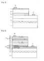
- FIG. 1 is a sectional view illustrating a conventional LED.
- the conventional LED comprises a substrate 11, a buffer layer 13, an undoped GaN layer 15, an n-type GaN contact layer 17, an active region 19, a p-type AlGaN clad layer 21, a p-type GaN contact layer 25, a transparent electrode 27, a p-electrode 29 and an n-electrode 31.
- the conventional LED has an active region 19 of a multiple quantum well structure having an InGaN well layer between the n-type and p-type contact layers 17 and 25, thereby improving light emitting efficiency. Further, light having a desired wavelength can be emitted by controlling the In content of the InGaN well layer in the multiple quantum well structure.
- a nitride-based compound semiconductor used in the conventional LED is generally grown on the heterogeneous substrate 11 such as sapphire.
- the lattice constant difference between sapphire and GaN crystals is large, and therefore, a strong tensile stress is generated in the GaN layer grown on the sapphire substrate.
- the tensile stress causes high-density crystal defects, e.g., dislocations to be generated in the GaN layer, and such dislocations are transferred to the active region 19 of the multiple quantum well structure, thereby reducing the light emitting efficiency.
- the strain generated in the multiple quantum well structure is influenced by an n-type nitride semiconductor layer adjacent to an active layer. As the mismatch of lattice constants between an n-type nitride semiconductor layer, e.g., an n-type contact layer, and a quantum well layer is increased, the strain induced in the active region is increased.
- a technique for forming a superlattice structure in which first and second nitride semiconductor layers having different compositions are alternately laminated between an n-type GaN contact layer and an active layer.
- the growth conditions of the respective layers e.g., temperatures and gas flow rates, are different. Therefore, a process of forming the superlattice structure is complicated, and process time is increased.
- the conventional LED allows current to be uniformly distributed in the p-type contact layer 25 by forming the transparent electrode 27 such as indium tin oxide (ITO) on the p-type contact layer 25.
- ITO indium tin oxide
- the current distribution using the transparent electrode 27 has a limitation due to its light transmittance and resistance. That is, as the transparent electrode 27 is increased in thickness, its light transmittance is rapidly decreased. When the resistance of the transparent electrode is excessively low, current flows into the sides of the transparent electrode and then flows out through the sides of the transparent electrode, so that light emitting efficiency may be reduced. On the other hand, when the thickness of the transparent electrode 27 is thin, it is difficult to uniformly distribute current on the p-type contact layer 25. Accordingly, although current distribution performance is ensured by optimizing the thickness of the transparent electrode 27, there is a limit in optimizing current distribution due to nonuniformity in thickness of the transparent electrode 27, crystal defects in the p-type contact layer 25, and the like.
- ESD electrostatic discharge
- a superlattice layer may be formed on the p-side region of the LED so as to improve the ESD characteristic.
- a superlattice layer having nitride semiconductor layers with different compositions is employed, manufacturing time of the LED is rapidly increased.
- modulation doped GaN layers may be used as an n-type contact layer (see EP 1063711 A1 ) to positively influence the light emission efficiency.
- An object of the present invention is to provide an LED, wherein dislocations can be prevented from being transferred into an active region while process time is prevented from being increased.
- Another object of the present invention is to provide an LED, in which strains induced in a multiple quantum well structure can be reduced.
- a further object of the present invention is to provide an LED, in which an electrostatic discharge characteristic is improved and a turn-on voltage is increased while process time is prevented from being increased.
- an LED having a modulation doped layer comprising an n-type contact layer, a p-type contact layer, and an active region of a multiple quantum well structure having an InGaN well layer and interposed between the n-type and p-type contact layers.
- the n-type contact layer comprises a first modulation doped layer having first InGaN layers and second InGaN layers alternately laminated, wherein the first InGaN layers are doped with an n-type impurity and the second InGaN layers have a lower doping concentration than that of the first InGaN layers, and a second modulation doped layer have third InGaN layers and fourth InGaN layers alternately laminated, wherein the third InGaN layers are doped with an n-type impurity and the fourth InGaN layers have a lower doping concentration than that of the third InGaN layers.
- first and second InGaN layers in the first modulation doped layer have the same composition
- third and fourth InGaN layers in the second modulation doped layer have the same composition
- the second modulation doped layer is interposed between the first modulation doped layer and the active region, and an n-electrode is in contact with the first modulation doped layer.
- the InGaN/InGaN modulation doped layer having the same composition is used as an n-type contact layer, so that it is possible to prevent process time of manufacturing an LED from being increased and dislocations from being transferred into the multiple quantum well structure through the modulation doped layer. Further, the InGaN/InGaN modulation doped layer is used, so that strains induced in the active region can be reduced as compared with a case where a GaN layer is used as a contact layer. Furthermore, the crystallinity of a quantum well layer is improved, thereby increasing the recombination rate of carriers.
- the second InGaN layer having a lower doping concentration than that of the first InGaN layer may be an undoped layer.
- the fourth InGaN layer having a lower doping concentration than that of the third InGaN layer may be an undoped layer.
- An In composition ratio in the first modulation doped layer may be smaller than that of the second modulation doped layer.
- the second modulation doped layer having a great In composition ratio is formed on the first modulation doped layer having a small In composition ratio, so that the In composition ratio can be gradually increased. Accordingly, it is possible to reduce strains caused by the difference in lattice constant between the n-type contact layer and the active region.
- the third InGaN layer doped with the n-type impurity in the second modulation doped layer may be adjacent to the active region. Accordingly, electrons can be smoothly injected into the active region from the modulation doped layer.
- the second modulation doped layer has a smaller In composition ratio than the InGaN well layer. Accordingly, carriers can be trapped in the active region, thereby increasing the recombination rate of electrons and holes.
- the LED may further comprise a substrate and a buffer layer interposed between the substrate and the n-type contact layer.
- the substrate may be a sapphire substrate, and the buffer layer may be a GaN buffer layer.
- the p-type contact layer may comprise a first p-type GaN layer, a second p-type GaN layer and a third modulation doped layer interposed between the first and second p-type GaN layers.
- the third modulation doped layer has fifth InGaN layers and sixth layers alternately laminated, wherein the fifth InGaN layers are doped with a p-type impurity and the sixth InGaN layers have a lower doping concentration than that of the fifth InGaN layers; and the fifth and sixth InGaN layers have the same composition. Accordingly, current distribution can be promoted in the p-type contact layer, thereby improving ESD and turn-on voltage characteristics of the LED.
- the sixth InGaN layer having a lower doping concentration than that of the fifth InGaN layer may be an undoped layer.
- the second p-type GaN layer may have the same doping concentration as the first p-type GaN layer.
- the fifth InGaN layer doped with the p-type impurity in the third modulation doped layer may have a different doping concentration from those of the first and second p-type GaN layers.
- the fifth InGaN layer may have a lower doping concentration than those of first and second p-type GaN layers.
- the LED may further comprise a p-type AlGaN clad layer interposed between the active region and the p-type contact layer.
- the p-type AlGaN clad layer prevents overflow of electrons, thereby increasing the recombination rate of electrons and holes.
- the LED may further comprise a superlattice layer interposed between the active region and the p-type AlGaN clad layer, wherein the superlattice layer have InGaN layers doped with a p-type impurity and AlGaN layers doped with a p-type impurity alternately laminated.
- the superlattice layer is used to reduce lattice mismatch between the multiple quantum well structure and the p-type AlGaN clad layer.
- FIG. 2 is a sectional view illustrating an LED according to one embodiment of the present invention.
- the LED comprises an n-type contact layer 57, an active region 59 of a multiple quantum well structure and a p-type contact layer 65.
- the LED may further comprise a substrate 51 and a buffer layer 55 interposed between the substrate 51 1 and the n-type contact layer 57.
- a nucleus layer 53 may be interposed between the substrate 51 and the buffer layer 55.
- a p-type AlGaN clad layer 61 may be interposed between the active region 59 and the p-type contact layer 65, and an InGaN/AlGaN superlattice layer 60 may be interposed between the p-type AlGaN clad layer 61 and the active region 59.
- a transparent electrode 67 and a p-electrode 69 may be formed on the p-type contact layer 65, and an n-electrode 71 may be formed on the n-type contact layer 57.
- the substrate 51 is a substrate for growing GaN-based semiconductor layers thereon, and includes, but not particularly limited to, sapphire, SiC, spinel and the like.
- the substrate 51 may be a patterned sapphire substrate (PSS) as shown in this figure.
- PSS patterned sapphire substrate
- the nucleus layer 53 may be formed of (Al, Ga)N, preferably GaN, at a low temperature of 400 to 600 °C so as to grow the GaN buffer layer 55 on the substrate 51.
- the nucleus layer 53 may be formed to have a thickness of about 25nm.
- the GaN buffer layer 55 is formed to reduce lattice mismatch between the substrate 51 and the n-type contact layer 57 and grown at a relatively high temperature.
- the GaN buffer layer may be formed of undoped GaN or GaN doped with an n-type impurity such as Si or Ge.
- the n-type contact layer 57 comprises a first modulation doped layer 56 and a second modulation doped layer 58, wherein the first modulation doped layer 56 has InGaN layers 56a doped with an n-type impurity and InGaN layers 56b having a lower doping concentration than that of the InGaN layers 56a, e.g., undoped InGaN layers 56b alternately laminated, and the second modulation doped layer 58 has InGaN layers 58a doped with an n-type impurity and InGaN layers 58b having a lower doping concentration than that of the InGaN layers 58a, e.g., undoped InGaN layers 58b alternately laminated.
- each of the first and second modulation doped layers 56 and 58 is formed of InGaN layers having the same composition except different impurity doping concentrations. Accordingly, each of the first and second modulation doped layers 56 and 58 may be formed by controlling the supply amount of an impurity source, e.g., by repeating the supply and interception of an impurity source.
- the second modulation doped layer 58 is interposed between the first modulation doped layer 56 and the active region 59.
- An In composition ratio in the first modulation doped layer 56 is different from that in the second modulation doped layer 58.
- the In composition ratio in the first modulation doped layer 56 is smaller than that in the second modulation doped layer 58. Accordingly, the In composition ratio in the n-type contact layer 57 can be gradually increased, so that the lattice mismatch between the n-type contact layer 57 and the active region 59 can be more reduced.
- the impurity with which the InGaN layers in the first and second modulation doped layers 56 and 58 are doped, may be various, including Si, Ge and the like. Preferably, Si may be used as the impurity. Si, with which the first and second modulation doped layers 56 and 58 are doped, prevents dislocations induced from its lower layer from being transferred to its upper layer, thereby improving crystallinity in the active region 59.
- the InGaN layers in each of the first and second modulation doped layers 56 and 58 may be formed by 7 to 15 periods.
- the effect of using modulation doped layers is slight when the InGaN layers in the first or second modulation doped layer 56 or 58 are formed by below 7 periods while process time is increased when the InGaN layers in the first or second modulation doped layer 56 or 58 are formed by over 15 periods, which is not preferable.
- the first and second modulation doped layers 56 and 58 may come into contact with each other.
- the present invention is not limited thereto. That is, a GaN-based semiconductor layer having a different composition from those of the first and second modulation doped layers may be interposed therebetween.
- the active region 59 has a multiple quantum well structure in which quantum barrier layers and InGaN quantum well layers are alternately laminated.
- the quantum barrier layer may be formed of a GaN-based semiconductor layer, e.g., GaN, InGaN, AlGaN or AlInGaN, having a wider bandgap than that of the quantum well layer.
- the In composition ratio in the InGaN quantum well layer is determined by a desired optical wavelength.
- the In composition ratio in the InGaN layer of the second modulation doped layer 58 is smaller than that of the InGaN quantum well layer such that electrons and holes can be trapped in the InGaN quantum well layer.
- the p-type clad layer 61 may be formed of AlGaN and allows a recombination rate of electrons and holes in the active region 59 to be improved by preventing overflow of electrons. Since the p-type AlGaN clad layer 61 has a relatively low lattice constant, the lattice mismatch between the active region 59 having the multiple quantum well structure and the clad layer 61 is increased, and therefore, the crystallinity of the AlGaN clad layer 61 may be deteriorated. Accordingly, before the AlGaN clad layer 61 is formed, the InGaN/AlGaN superlattice layer 60 may be formed. The superlattice layer 60 serves as a buffer layer for the p-type AlGaN clad layer 61.
- the p-type contact layer 65 comprises a first p-type GaN layer 62, a third modulation doped layer 63 and a second p-type GaN layer 64.
- the first and second p-type GaN layers 62 and 64 may be grown at a temperature of about 950 °C using a metal organic chemical vapor deposition (MOCVD) technique and doped with a p-type impurity, e.g., Mg at a concentration of about 5x10 18 cm -3 .
- MOCVD metal organic chemical vapor deposition
- the first and second p-type GaN layers 62 and 64 have the same doping concentration so as to perform a stable process.
- In the third modulation doped layer 63 InGaN layers 63a doped with a p-type impurity and InGaN layers 63b, e.g., undoped InGaN layers 63b, having a lower doping concentration than that of the InGaN layer 63a are alternately laminated.
- the InGaN layers 63a and 63b in the third modulation doped layer 63 may be grown by 7 to 15 periods.
- the InGaN layers 63a may be doped with Mg at a concentration of about 1x10 17 - 1x10 18 cm -3 , which is lower than that of the first and second p-type GaN layers 62 and 64.
- These InGaN layers 63a and 63b are formed to have the same composition except for doping or not with an impurity. Accordingly, the third modulation doped layer 63 may be continuously grown at the same temperature by repeating the supply and interception of a source gas of a p-type impurity, e.g., Cp 2 Mg.
- a source gas of a p-type impurity e.g., Cp 2 Mg.
- the doped InGaN layer 63a and the undoped InGaN layer 63b are repeatedly laminated in the third modulation doped layer 63, current can be easily distributed in the InGaN layer 63a. As a result, current can be uniformly distributed in the p-type contact layer 65. Further, the crystallinity of the second p-type GaN layer 64 can be improved by the third modulation doped layer 63.
- the transparent electrode 67 such as Ni/Au or indium tin oxide (ITO) is formed on the p-type contact layer 65, and the p-electrode 69 may be formed on the transparent electrode 67 using a lift-off process, for example.
- the n-electrode 71 such as Ni/Au or Ti/Al may also be formed on the n-type contact layer 57 by a lift-off process.
- the n-electrode 71 is preferably formed on the first modulation doped layer 56, as shown in this figure.
- the LED has been described in which the p-electrode 69 and the n-electrode 71 are formed on top of the substrate 51, the present invention is not limited thereto.
- the LED according to the present invention may be a vertical LED, in which electrodes are respectively formed on top and bottom surfaces of an LED through the process of separating the substrate 51 by a laser lift-off process.
- LEDs of present example and comparative example were manufactured to have the same structure except for application or not of the third modulation doped layer 63. That is, an LED (Present Example) was manufactured by growing the first p-type GaN layer 62, the Mg-doped InGaN layers and the undoped InGaN layers, and the second p-type GaN layer 64 and then forming an ITO transparent electrode 67, wherein the first p-type GaN layer 62 doped with Mg at a concentration of 5x10 18 cm -3 was formed to have a thickness of 50nm, the Mg-doped and undoped InGaN layers each having a thickness of 22 ⁇ were formed in 10 periods to have a total thickness of 22nm, the second p-type GaN layer 64 doped with Mg at a concentration of 5x10 18 cm -3 was formed to have a thickness of 128nm.
- an LED Compar
- an InGaN/InGaN modulation doped layer is used, so that it is possible to reduce strains in a multiple quantum well structure and to prevent dislocations from being transferred into the multiple quantum well structure through an n-type contact layer.
- a modulation doped layer is formed using InGaN layers having the same composition except an impurity, the InGaN layers in the modulation doped layer can be grown at the same temperature, thereby preventing an increase in manufacturing time.
- first and second modulation doped layers have different compositions from each other, so that the In composition ratio in an n-type contact layer can be gradually increased. Accordingly, the lattice mismatch between the n-type contact layer and a quantum well layer can be more reduced.
- an InGaN/InGaN modulation doped layer is formed in a p-type contact layer, so that current distribution can be promoted in the p-type contact layer, which makes it possible to improve ESD and turn-on voltage characteristics of an LED.
Landscapes
- Led Devices (AREA)
Claims (22)
- Lichtemittierende Diode (LED), umfassend eine Kontaktschicht vom n-Typ, eine Kontaktschicht vom p-Typ und einen aktiven Bereich mit Mehrfach-Quantentopfstruktur, der eine InGaN-Quantentopfschicht aufweist und zwischen der Kontaktschichten vom n-Typ und vom p-Typ angeordnet ist,
wobei die Kontaktschicht vom n-Typ eine erste modulationsdotierte Schicht mit abwechselnd laminierten ersten InGaN-Schichten und zweiten InGaN-Schichten umfasst, die ersten InGaN-Schichten mit einem Fremdstoff vom n-Typ dotiert sind und die zweiten InGaN-Schichten eine niedrigere Dotierungskonzentration als die ersten InGaN-Schichten aufweisen, und eine zweite modulationsdotierte Schicht mit abwechselnd laminierten dritten InGaN-Schichten und vierten InGaN-Schichten umfasst, die dritten InGaN-Schichten mit einem Fremdstoff vom n-Typ dotiert sind und die vierten InGaN-Schichten eine niedrigere Dotierungskonzentration als die dritten InGaN-Schichten aufweisen;
die ersten und zweiten InGaN-Schichten in der ersten modulationsdotierten Schicht dieselbe Zusammensetzung und die dritten und vierten InGaN-Schichten in der zweiten modulationsdotierten Schicht dieselbe Zusammensetzung aufweisen;
die zweite modulationsdotierte Schicht zwischen der ersten modulationsdotierten Schicht und dem aktiven Bereich angeordnet ist; und
eine n-Elektrode in Kontakt mit der ersten modulationsdotierten Schicht ist. - LED, wie sie in Anspruch 1 beansprucht wird, wobei sich der In-Anteil in der Zusammensetzung der ersten modulationsdotierten Schicht vom demjenigen in der zweiten modulationsdotierten Schicht unterscheidet.
- LED, wie sie in Anspruch 2 beansprucht wird, wobei der In-Anteil in der Zusammensetzung der ersten modulationsdotierten Schicht kleiner ist als derjenige in der zweiten modulationsdotierten Schicht.
- LED, wie sie in Anspruch 1 beansprucht wird, wobei die mit dem Fremdstoff vom n-Typ dotierte dritte InGaN-Schicht in der zweiten modulationsdotierten Schicht an den aktiven Bereich angrenzt.
- LED, wie sie in Anspruch 1 beansprucht wird, wobei die zweite modulationsdotierte Schicht einen kleineren In-Anteil in der Zusammensetzung aufweist als die InGaN-Quantentopfschicht.
- LED, wie sie in Anspruch 1 beansprucht wird, wobei die zweite InGaN-Schicht, die eine geringere Dotierungskonzentration als die erste InGaN-Schicht aufweist, eine undotierte Schicht ist.
- LED, wie sie in Anspruch 1 beansprucht wird, wobei die vierte InGaN-Schicht, die eine geringere Dotierungskonzentration als die dritte InGaN-Schicht aufweist, eine undotierte Schicht ist.
- LED, wie sie in Anspruch 1 beansprucht wird, weiterhin umfassend ein Saphirsubstrat und eine GaN-Pufferschicht, die zwischen dem Saphirsubstrat und der Kontaktschicht vom n-Typ angeordnet ist.
- LED, wie sie in Anspruch 1 beansprucht wird, wobei die Kontaktschicht vom p-Typ eine erste GaN-Schicht vom p-Typ, eine zweite GaN-Schicht vom p-Typ und eine zwischen der ersten und zweiten GaN-Schicht vom p-Typ angeordnete dritte modulationsdotierte Schicht umfasst; wobei die dritte modulationsdotierte Schicht abwechselnd laminierte fünfte InGaN-Schichten und sechste InGaN-Schichten aufweist, die fünften InGaN-Schichten mit einem Fremdstoff vom p-Typ dotiert sind, die sechsten InGaN-Schichten eine niedrigere Dotierungskonzentration als die fünften InGaN-Schichten aufweisen, und die fünften und sechsten InGaN-Schichten dieselbe Zusammensetzung aufweisen.
- LED, wie sie in Anspruch 9 beansprucht wird, wobei die zweite GaN-Schicht vom p-Typ dieselbe Dotierungskonzentration wie die erste GaN-Schicht vom p-Typ aufweist.
- LED, wie sie in Anspruch 9 beansprucht wird, wobei die mit dem Fremdstoff vom p-Typ dotierte fünfte InGaN-Schicht in der dritten modulationsdotierten Schicht eine andere Dotierungskonzentration als die erste und zweite GaN-Schicht vom p-Typ aufweist.
- LED, wie sie in Anspruch 11 beansprucht wird, wobei die mit dem Fremdstoff vom p-Typ dotierte fünfte InGaN-Schicht in der dritten modulationsdotierten Schicht eine niedrigere Dotierungskonzentration als die erste und zweite GaN-Schicht vom p-Typ aufweist.
- LED, wie sie in Anspruch 9 beansprucht wird, wobei die sechste InGaN-Schicht, die eine niedrigere Dotierungskonzentration als die fünfte InGaN-Schicht aufweist, eine undotierte Schicht ist.
- LED, wie sie in Anspruch 9 beansprucht wird, weiterhin umfassend eine AIGaN-Plattierungsschicht vom p-Typ, die zwischen dem aktiven Bereich und der Kontaktschicht vom p-Typ angeordnet ist.
- LED, wie sie in Anspruch 14 beansprucht wird, weiterhin umfassend eine zwischen dem aktiven Bereich und der AIGaN-Plattierungsschicht vom p-Typ angeordnete Übergitterschicht, wobei die Übergitterschicht abwechselnd laminierte mit einem Fremdstoff vom p-Typ dotierte InGaN-Schichten und mit einem Fremdstoff vom p-Typ dotierte AIGaN-Schichten aufweist.
- LED, umfassend:eine Kontaktschicht vom n-Typ,eine über der Kontaktschicht vom n-Typ gebildete Kontaktschicht vom p-Typ; undeinen aktiven Bereich mit Mehrfach-Quantentopfstruktur, der eine InGaN-Quantentopfschicht aufweist, wobei der aktive Bereich zwischen der Kontaktschicht vom n-Typ und der Kontaktschicht vom p-Typ angeordnet ist,wobei die Kontaktschicht vom p-Typ eine erste GaN-Schicht vom p-Typ, eine zweite GaN-Schicht vom p-Typ und eine zwischen der ersten und zweiten GaN-Schicht vom p-Typ angeordnete modulationsdotierte Schicht umfasst;die modulationsdotierte Schicht abwechselnd laminierte fünfte InGaN-Schichten und sechste InGaN-Schichten umfasst, wobei die fünften InGaN-Schichten mit einem Fremdstoff vom p-Typ dotiert sind, die sechsten InGaN-Schichten eine niedrigere Dotierungskonzentration als die fünften InGaN-Schichten aufweisen; unddie fünften und sechsten InGaN-Schichten dieselbe Zusammensetzung aufweisen.
- LED, wie sie in Anspruch 16 beansprucht wird, wobei die zweite GaN-Schicht vom p-Typ dieselbe Dotierungskonzentration wie die erste GaN-Schicht vom p-Typ aufweist.
- LED, wie sie in Anspruch 16 beansprucht wird, wobei die mit dem Fremdstoff vom p-Typ dotierte fünfte InGaN-Schicht in der modulationsdotierten Schicht eine andere Dotierungskonzentration als die erste und zweite GaN-Schicht vom p-Typ aufweist.
- LED, wie sie in Anspruch 18 beansprucht wird, wobei die mit dem Fremdstoff vom p-Typ dotierte fünfte InGaN-Schicht in der modulationsdotierten Schicht eine niedrigere Dotierungskonzentration als die erste und zweite GaN-Schicht vom p-Typ aufweist.
- LED, wie sie in Anspruch 16 beansprucht wird, wobei die sechste InGaN-Schicht, die eine niedrigere Dotierungskonzentration als die fünfte InGaN-Schicht aufweist, eine undotierte Schicht ist.
- LED, wie sie in Anspruch 16 beansprucht wird, weiterhin umfassend eine AIGaN-Plattierungsschicht vom p-Typ, die zwischen dem aktiven Bereich und der Kontaktschicht vom p-Typ angeordnet ist.
- LED, wie sie in Anspruch 21 beansprucht wird, weiterhin umfassend eine zwischen dem aktiven Bereich und der AIGaN-Plattierungsschicht vom p-Typ angeordnete Übergitterschicht, wobei die Übergitterschicht abwechselnd laminierte mit einem Fremdstoff vom p-Typ dotierte InGaN-Schichten und mit einem Fremdstoff vom p-Typ dotierte AIGaN-Schichten aufweist.
Applications Claiming Priority (3)
| Application Number | Priority Date | Filing Date | Title |
|---|---|---|---|
| KR20080081172 | 2008-08-20 | ||
| KR1020090060021A KR101017396B1 (ko) | 2008-08-20 | 2009-07-02 | 변조도핑층을 갖는 발광 다이오드 |
| PCT/KR2009/003637 WO2010021457A2 (ko) | 2008-08-20 | 2009-07-03 | 변조도핑층을 갖는 발광 다이오드 |
Publications (3)
| Publication Number | Publication Date |
|---|---|
| EP2325902A2 EP2325902A2 (de) | 2011-05-25 |
| EP2325902A4 EP2325902A4 (de) | 2013-04-24 |
| EP2325902B1 true EP2325902B1 (de) | 2014-03-12 |
Family
ID=42175327
Family Applications (1)
| Application Number | Title | Priority Date | Filing Date |
|---|---|---|---|
| EP09808363.7A Active EP2325902B1 (de) | 2008-08-20 | 2009-07-03 | Leuchtdiode mit modulationsdotierter schicht |
Country Status (5)
| Country | Link |
|---|---|
| US (2) | US7982210B2 (de) |
| EP (1) | EP2325902B1 (de) |
| JP (1) | JP5523459B2 (de) |
| KR (1) | KR101017396B1 (de) |
| WO (1) | WO2010021457A2 (de) |
Families Citing this family (38)
| Publication number | Priority date | Publication date | Assignee | Title |
|---|---|---|---|---|
| KR100703096B1 (ko) * | 2005-10-17 | 2007-04-06 | 삼성전기주식회사 | 질화물 반도체 발광 소자 |
| KR101628233B1 (ko) * | 2010-07-08 | 2016-06-08 | 엘지이노텍 주식회사 | 발광 다이오드 및 이를 포함하는 발광 소자 패키지 |
| US20120049151A1 (en) * | 2010-08-30 | 2012-03-01 | Invenlux Corporation | Light-emitting devices with two-dimensional composition-fluctuation active-region and method for fabricating the same |
| KR101259482B1 (ko) * | 2010-09-24 | 2013-05-06 | 서울옵토디바이스주식회사 | 고효율 발광다이오드 |
| JP5648475B2 (ja) * | 2010-12-28 | 2015-01-07 | 信越半導体株式会社 | 発光素子 |
| CN102637793B (zh) | 2011-02-15 | 2015-08-12 | 展晶科技(深圳)有限公司 | 三族氮化合物半导体紫外光发光二极管 |
| KR20120100056A (ko) * | 2011-03-02 | 2012-09-12 | 엘지이노텍 주식회사 | 발광 소자 |
| TW201238043A (en) * | 2011-03-11 | 2012-09-16 | Chi Mei Lighting Tech Corp | Light-emitting diode device and method for manufacturing the same |
| CN102157646A (zh) * | 2011-05-03 | 2011-08-17 | 映瑞光电科技(上海)有限公司 | 一种氮化物led结构及其制备方法 |
| JP5023230B1 (ja) | 2011-05-16 | 2012-09-12 | 株式会社東芝 | 窒化物半導体素子、窒化物半導体ウェーハ及び窒化物半導体層の製造方法 |
| JP5601281B2 (ja) * | 2011-05-30 | 2014-10-08 | 豊田合成株式会社 | Iii族窒化物半導体発光素子の製造方法 |
| JP5598437B2 (ja) * | 2011-07-12 | 2014-10-01 | 豊田合成株式会社 | Iii族窒化物半導体発光素子の製造方法 |
| US9012939B2 (en) * | 2011-08-02 | 2015-04-21 | Kabushiki Kaisha Toshiba | N-type gallium-nitride layer having multiple conductive intervening layers |
| JP5238865B2 (ja) * | 2011-10-11 | 2013-07-17 | 株式会社東芝 | 半導体発光素子 |
| KR20130058406A (ko) * | 2011-11-25 | 2013-06-04 | 삼성전자주식회사 | 반도체 발광소자 |
| KR101903361B1 (ko) * | 2012-03-07 | 2018-10-04 | 삼성전자주식회사 | 질화물 반도체 발광소자 및 그 제조방법 |
| KR101997020B1 (ko) * | 2012-03-29 | 2019-07-08 | 서울바이오시스 주식회사 | 근자외선 발광 소자 |
| US10164150B2 (en) * | 2012-03-29 | 2018-12-25 | Seoul Viosys Co., Ltd. | Near UV light emitting device |
| KR102246648B1 (ko) * | 2014-07-29 | 2021-04-30 | 서울바이오시스 주식회사 | 자외선 발광 다이오드 |
| TWI499080B (zh) | 2012-11-19 | 2015-09-01 | Genesis Photonics Inc | 氮化物半導體結構及半導體發光元件 |
| TWI524551B (zh) | 2012-11-19 | 2016-03-01 | 新世紀光電股份有限公司 | 氮化物半導體結構及半導體發光元件 |
| TWI535055B (zh) | 2012-11-19 | 2016-05-21 | 新世紀光電股份有限公司 | 氮化物半導體結構及半導體發光元件 |
| CN103972342A (zh) * | 2013-01-25 | 2014-08-06 | 新世纪光电股份有限公司 | 氮化物半导体结构及半导体发光元件 |
| JP2014183285A (ja) * | 2013-03-21 | 2014-09-29 | Stanley Electric Co Ltd | 発光素子 |
| KR102053388B1 (ko) * | 2013-06-11 | 2019-12-06 | 엘지이노텍 주식회사 | 발광소자 |
| US10109767B2 (en) * | 2014-04-25 | 2018-10-23 | Seoul Viosys Co., Ltd. | Method of growing n-type nitride semiconductor, light emitting diode and method of fabricating the same |
| US9985168B1 (en) | 2014-11-18 | 2018-05-29 | Cree, Inc. | Group III nitride based LED structures including multiple quantum wells with barrier-well unit interface layers |
| TWI568016B (zh) * | 2014-12-23 | 2017-01-21 | 錼創科技股份有限公司 | 半導體發光元件 |
| KR102643093B1 (ko) * | 2017-01-25 | 2024-03-04 | 쑤저우 레킨 세미컨덕터 컴퍼니 리미티드 | 반도체 소자 및 조명장치 |
| JP6669095B2 (ja) * | 2017-02-06 | 2020-03-18 | 日亜化学工業株式会社 | 窒化物半導体発光素子の製造方法 |
| US10403794B2 (en) * | 2017-03-30 | 2019-09-03 | Epistar Corporation | Semiconductor device |
| KR102432226B1 (ko) * | 2017-12-01 | 2022-08-12 | 쑤저우 레킨 세미컨덕터 컴퍼니 리미티드 | 반도체 소자 |
| US11393948B2 (en) | 2018-08-31 | 2022-07-19 | Creeled, Inc. | Group III nitride LED structures with improved electrical performance |
| US11366153B2 (en) * | 2019-01-15 | 2022-06-21 | Kkt Holdings Syndicate | Micro LED display panel |
| KR102540198B1 (ko) * | 2020-05-22 | 2023-06-02 | 충칭 콘카 포토일렉트릭 테크놀로지 리서치 인스티튜트 컴퍼니 리미티드 | 초격자층, led 에피택셜 구조, 디스플레이 장치 및 이의 제조 방법 |
| JP7333504B2 (ja) * | 2020-11-16 | 2023-08-25 | 日亜化学工業株式会社 | 発光素子 |
| JP7539338B2 (ja) * | 2021-04-15 | 2024-08-23 | 日機装株式会社 | 半導体発光素子 |
| CN121262955B (zh) * | 2025-11-24 | 2026-04-24 | 天津工业大学 | 一种多波长光谱可控的紫外发光二极管结构及其制备方法 |
Family Cites Families (18)
| Publication number | Priority date | Publication date | Assignee | Title |
|---|---|---|---|---|
| EP1014455B1 (de) * | 1997-07-25 | 2006-07-12 | Nichia Corporation | Halbleitervorrichtung aus einer nitridverbindung |
| CA2322490C (en) * | 1998-03-12 | 2010-10-26 | Nichia Chemical Industries, Ltd. | Nitride semiconductor device |
| JP3680558B2 (ja) * | 1998-05-25 | 2005-08-10 | 日亜化学工業株式会社 | 窒化物半導体素子 |
| JP3063756B1 (ja) * | 1998-10-06 | 2000-07-12 | 日亜化学工業株式会社 | 窒化物半導体素子 |
| JP3470622B2 (ja) * | 1998-11-18 | 2003-11-25 | 日亜化学工業株式会社 | 窒化物半導体発光素子 |
| JP2000261035A (ja) * | 1999-03-12 | 2000-09-22 | Toyoda Gosei Co Ltd | GaN系の半導体素子 |
| JP3763701B2 (ja) * | 1999-05-17 | 2006-04-05 | 株式会社東芝 | 窒化ガリウム系半導体発光素子 |
| US7692182B2 (en) * | 2001-05-30 | 2010-04-06 | Cree, Inc. | Group III nitride based quantum well light emitting device structures with an indium containing capping structure |
| JP3543809B2 (ja) * | 2001-07-04 | 2004-07-21 | 日亜化学工業株式会社 | 窒化物半導体素子 |
| JP4032704B2 (ja) | 2001-10-23 | 2008-01-16 | 日亜化学工業株式会社 | 窒化物半導体素子 |
| JP2003218396A (ja) * | 2001-11-15 | 2003-07-31 | Mitsubishi Cable Ind Ltd | 紫外線発光素子 |
| JP2004014587A (ja) * | 2002-06-04 | 2004-01-15 | Hitachi Cable Ltd | 窒化物系化合物半導体エピタキシャルウエハ及び発光素子 |
| JP2004214337A (ja) * | 2002-12-27 | 2004-07-29 | Nichia Chem Ind Ltd | 窒化物半導体発光素子 |
| KR100765004B1 (ko) * | 2004-12-23 | 2007-10-09 | 엘지이노텍 주식회사 | 질화물 반도체 발광소자 및 그 제조방법 |
| KR100604423B1 (ko) | 2005-08-02 | 2006-07-25 | 삼성전기주식회사 | 질화물 반도체 소자 |
| DE102006046227A1 (de) * | 2006-07-27 | 2008-01-31 | Osram Opto Semiconductors Gmbh | Halbleiter-Schichtstruktur mit Übergitter |
| KR20090034169A (ko) * | 2007-10-02 | 2009-04-07 | 주식회사 에피밸리 | 3족 질화물 반도체 발광소자 |
| KR20090056319A (ko) * | 2007-11-30 | 2009-06-03 | 한국광기술원 | 초격자 구조를 가지는 질화물계 반도체 발광소자 |
-
2009
- 2009-07-02 KR KR1020090060021A patent/KR101017396B1/ko not_active Expired - Fee Related
- 2009-07-03 EP EP09808363.7A patent/EP2325902B1/de active Active
- 2009-07-03 JP JP2011523731A patent/JP5523459B2/ja not_active Expired - Fee Related
- 2009-07-03 WO PCT/KR2009/003637 patent/WO2010021457A2/ko not_active Ceased
- 2009-08-12 US US12/540,123 patent/US7982210B2/en not_active Expired - Fee Related
-
2011
- 2011-05-09 US US13/103,631 patent/US8247792B2/en active Active
Also Published As
| Publication number | Publication date |
|---|---|
| US20110204326A1 (en) | 2011-08-25 |
| KR101017396B1 (ko) | 2011-02-28 |
| JP5523459B2 (ja) | 2014-06-18 |
| EP2325902A4 (de) | 2013-04-24 |
| US8247792B2 (en) | 2012-08-21 |
| KR20100022913A (ko) | 2010-03-03 |
| WO2010021457A3 (ko) | 2010-04-15 |
| US20100044674A1 (en) | 2010-02-25 |
| US7982210B2 (en) | 2011-07-19 |
| JP2012500489A (ja) | 2012-01-05 |
| EP2325902A2 (de) | 2011-05-25 |
| WO2010021457A2 (ko) | 2010-02-25 |
Similar Documents
| Publication | Publication Date | Title |
|---|---|---|
| EP2325902B1 (de) | Leuchtdiode mit modulationsdotierter schicht | |
| EP2523228B1 (de) | Lichtemittierende diode | |
| US8044385B2 (en) | Semiconductor light emitting device and method for manufacturing the same | |
| KR102191213B1 (ko) | 자외선 발광 소자 | |
| US8896085B2 (en) | Semiconductor light-emitting element manufacturing method, lamp, electronic equipment, and mechanical apparatus | |
| US20140084242A1 (en) | Group iii nitride semiconductor light-emitting device | |
| JP5504618B2 (ja) | Iii族窒化物半導体発光素子及びその製造方法 | |
| KR101997020B1 (ko) | 근자외선 발광 소자 | |
| US20150179881A1 (en) | Nitride led structure with double graded electron blocking layer | |
| KR20110084683A (ko) | 양자우물 구조의 활성 영역을 갖는 발광 소자 | |
| KR100979701B1 (ko) | 변조도핑층을 갖는 발광 다이오드 | |
| KR101507128B1 (ko) | 인듐질화물을 포함하는 발광 다이오드 | |
| KR101507130B1 (ko) | 초격자층을 갖는 발광 다이오드 | |
| KR20100024154A (ko) | 발광 다이오드 | |
| KR101583276B1 (ko) | 전류 분산을 위한 다층 구조체를 갖는 발광 다이오드 | |
| JP5942519B2 (ja) | 半導体発光素子 | |
| KR20100022593A (ko) | 발광 다이오드 |
Legal Events
| Date | Code | Title | Description |
|---|---|---|---|
| PUAI | Public reference made under article 153(3) epc to a published international application that has entered the european phase |
Free format text: ORIGINAL CODE: 0009012 |
|
| 17P | Request for examination filed |
Effective date: 20110216 |
|
| AK | Designated contracting states |
Kind code of ref document: A2 Designated state(s): AT BE BG CH CY CZ DE DK EE ES FI FR GB GR HR HU IE IS IT LI LT LU LV MC MK MT NL NO PL PT RO SE SI SK SM TR |
|
| AX | Request for extension of the european patent |
Extension state: AL BA RS |
|
| DAX | Request for extension of the european patent (deleted) | ||
| A4 | Supplementary search report drawn up and despatched |
Effective date: 20130327 |
|
| RIC1 | Information provided on ipc code assigned before grant |
Ipc: H01S 5/30 20060101ALI20130321BHEP Ipc: H01L 33/04 20100101AFI20130321BHEP |
|
| RIC1 | Information provided on ipc code assigned before grant |
Ipc: H01L 33/02 20100101ALN20131003BHEP Ipc: H01S 5/30 20060101ALI20131003BHEP Ipc: H01L 33/32 20100101ALN20131003BHEP Ipc: H01L 33/04 20100101AFI20131003BHEP |
|
| GRAP | Despatch of communication of intention to grant a patent |
Free format text: ORIGINAL CODE: EPIDOSNIGR1 |
|
| INTG | Intention to grant announced |
Effective date: 20131114 |
|
| GRAS | Grant fee paid |
Free format text: ORIGINAL CODE: EPIDOSNIGR3 |
|
| GRAA | (expected) grant |
Free format text: ORIGINAL CODE: 0009210 |
|
| AK | Designated contracting states |
Kind code of ref document: B1 Designated state(s): AT BE BG CH CY CZ DE DK EE ES FI FR GB GR HR HU IE IS IT LI LT LU LV MC MK MT NL NO PL PT RO SE SI SK SM TR |
|
| REG | Reference to a national code |
Ref country code: GB Ref legal event code: FG4D |
|
| REG | Reference to a national code |
Ref country code: CH Ref legal event code: EP |
|
| REG | Reference to a national code |
Ref country code: AT Ref legal event code: REF Ref document number: 656802 Country of ref document: AT Kind code of ref document: T Effective date: 20140315 |
|
| REG | Reference to a national code |
Ref country code: IE Ref legal event code: FG4D |
|
| REG | Reference to a national code |
Ref country code: NL Ref legal event code: T3 |
|
| REG | Reference to a national code |
Ref country code: DE Ref legal event code: R096 Ref document number: 602009022497 Country of ref document: DE Effective date: 20140424 |
|
| RAP2 | Party data changed (patent owner data changed or rights of a patent transferred) |
Owner name: SEOUL VIOSYS CO., LTD |
|
| PG25 | Lapsed in a contracting state [announced via postgrant information from national office to epo] |
Ref country code: LT Free format text: LAPSE BECAUSE OF FAILURE TO SUBMIT A TRANSLATION OF THE DESCRIPTION OR TO PAY THE FEE WITHIN THE PRESCRIBED TIME-LIMIT Effective date: 20140312 Ref country code: NO Free format text: LAPSE BECAUSE OF FAILURE TO SUBMIT A TRANSLATION OF THE DESCRIPTION OR TO PAY THE FEE WITHIN THE PRESCRIBED TIME-LIMIT Effective date: 20140612 |
|
| REG | Reference to a national code |
Ref country code: AT Ref legal event code: MK05 Ref document number: 656802 Country of ref document: AT Kind code of ref document: T Effective date: 20140312 |
|
| REG | Reference to a national code |
Ref country code: LT Ref legal event code: MG4D |
|
| PG25 | Lapsed in a contracting state [announced via postgrant information from national office to epo] |
Ref country code: SE Free format text: LAPSE BECAUSE OF FAILURE TO SUBMIT A TRANSLATION OF THE DESCRIPTION OR TO PAY THE FEE WITHIN THE PRESCRIBED TIME-LIMIT Effective date: 20140312 Ref country code: CY Free format text: LAPSE BECAUSE OF FAILURE TO SUBMIT A TRANSLATION OF THE DESCRIPTION OR TO PAY THE FEE WITHIN THE PRESCRIBED TIME-LIMIT Effective date: 20140312 Ref country code: FI Free format text: LAPSE BECAUSE OF FAILURE TO SUBMIT A TRANSLATION OF THE DESCRIPTION OR TO PAY THE FEE WITHIN THE PRESCRIBED TIME-LIMIT Effective date: 20140312 |
|
| PG25 | Lapsed in a contracting state [announced via postgrant information from national office to epo] |
Ref country code: LV Free format text: LAPSE BECAUSE OF FAILURE TO SUBMIT A TRANSLATION OF THE DESCRIPTION OR TO PAY THE FEE WITHIN THE PRESCRIBED TIME-LIMIT Effective date: 20140312 Ref country code: HR Free format text: LAPSE BECAUSE OF FAILURE TO SUBMIT A TRANSLATION OF THE DESCRIPTION OR TO PAY THE FEE WITHIN THE PRESCRIBED TIME-LIMIT Effective date: 20140312 |
|
| PG25 | Lapsed in a contracting state [announced via postgrant information from national office to epo] |
Ref country code: RO Free format text: LAPSE BECAUSE OF FAILURE TO SUBMIT A TRANSLATION OF THE DESCRIPTION OR TO PAY THE FEE WITHIN THE PRESCRIBED TIME-LIMIT Effective date: 20140312 Ref country code: EE Free format text: LAPSE BECAUSE OF FAILURE TO SUBMIT A TRANSLATION OF THE DESCRIPTION OR TO PAY THE FEE WITHIN THE PRESCRIBED TIME-LIMIT Effective date: 20140312 Ref country code: BE Free format text: LAPSE BECAUSE OF FAILURE TO SUBMIT A TRANSLATION OF THE DESCRIPTION OR TO PAY THE FEE WITHIN THE PRESCRIBED TIME-LIMIT Effective date: 20140312 Ref country code: IS Free format text: LAPSE BECAUSE OF FAILURE TO SUBMIT A TRANSLATION OF THE DESCRIPTION OR TO PAY THE FEE WITHIN THE PRESCRIBED TIME-LIMIT Effective date: 20140712 Ref country code: CZ Free format text: LAPSE BECAUSE OF FAILURE TO SUBMIT A TRANSLATION OF THE DESCRIPTION OR TO PAY THE FEE WITHIN THE PRESCRIBED TIME-LIMIT Effective date: 20140312 Ref country code: BG Free format text: LAPSE BECAUSE OF FAILURE TO SUBMIT A TRANSLATION OF THE DESCRIPTION OR TO PAY THE FEE WITHIN THE PRESCRIBED TIME-LIMIT Effective date: 20140612 |
|
| PG25 | Lapsed in a contracting state [announced via postgrant information from national office to epo] |
Ref country code: ES Free format text: LAPSE BECAUSE OF FAILURE TO SUBMIT A TRANSLATION OF THE DESCRIPTION OR TO PAY THE FEE WITHIN THE PRESCRIBED TIME-LIMIT Effective date: 20140312 Ref country code: SK Free format text: LAPSE BECAUSE OF FAILURE TO SUBMIT A TRANSLATION OF THE DESCRIPTION OR TO PAY THE FEE WITHIN THE PRESCRIBED TIME-LIMIT Effective date: 20140312 Ref country code: AT Free format text: LAPSE BECAUSE OF FAILURE TO SUBMIT A TRANSLATION OF THE DESCRIPTION OR TO PAY THE FEE WITHIN THE PRESCRIBED TIME-LIMIT Effective date: 20140312 Ref country code: PL Free format text: LAPSE BECAUSE OF FAILURE TO SUBMIT A TRANSLATION OF THE DESCRIPTION OR TO PAY THE FEE WITHIN THE PRESCRIBED TIME-LIMIT Effective date: 20140312 |
|
| REG | Reference to a national code |
Ref country code: DE Ref legal event code: R097 Ref document number: 602009022497 Country of ref document: DE |
|
| PG25 | Lapsed in a contracting state [announced via postgrant information from national office to epo] |
Ref country code: PT Free format text: LAPSE BECAUSE OF FAILURE TO SUBMIT A TRANSLATION OF THE DESCRIPTION OR TO PAY THE FEE WITHIN THE PRESCRIBED TIME-LIMIT Effective date: 20140714 |
|
| PLBE | No opposition filed within time limit |
Free format text: ORIGINAL CODE: 0009261 |
|
| STAA | Information on the status of an ep patent application or granted ep patent |
Free format text: STATUS: NO OPPOSITION FILED WITHIN TIME LIMIT |
|
| PG25 | Lapsed in a contracting state [announced via postgrant information from national office to epo] |
Ref country code: DK Free format text: LAPSE BECAUSE OF FAILURE TO SUBMIT A TRANSLATION OF THE DESCRIPTION OR TO PAY THE FEE WITHIN THE PRESCRIBED TIME-LIMIT Effective date: 20140312 |
|
| 26N | No opposition filed |
Effective date: 20141215 |
|
| PG25 | Lapsed in a contracting state [announced via postgrant information from national office to epo] |
Ref country code: LU Free format text: LAPSE BECAUSE OF FAILURE TO SUBMIT A TRANSLATION OF THE DESCRIPTION OR TO PAY THE FEE WITHIN THE PRESCRIBED TIME-LIMIT Effective date: 20140703 |
|
| REG | Reference to a national code |
Ref country code: CH Ref legal event code: PL |
|
| REG | Reference to a national code |
Ref country code: DE Ref legal event code: R097 Ref document number: 602009022497 Country of ref document: DE Effective date: 20141215 |
|
| PG25 | Lapsed in a contracting state [announced via postgrant information from national office to epo] |
Ref country code: IT Free format text: LAPSE BECAUSE OF FAILURE TO SUBMIT A TRANSLATION OF THE DESCRIPTION OR TO PAY THE FEE WITHIN THE PRESCRIBED TIME-LIMIT Effective date: 20140312 |
|
| REG | Reference to a national code |
Ref country code: IE Ref legal event code: MM4A |
|
| REG | Reference to a national code |
Ref country code: FR Ref legal event code: ST Effective date: 20150331 |
|
| PG25 | Lapsed in a contracting state [announced via postgrant information from national office to epo] |
Ref country code: CH Free format text: LAPSE BECAUSE OF NON-PAYMENT OF DUE FEES Effective date: 20140731 Ref country code: LI Free format text: LAPSE BECAUSE OF NON-PAYMENT OF DUE FEES Effective date: 20140731 |
|
| PG25 | Lapsed in a contracting state [announced via postgrant information from national office to epo] |
Ref country code: FR Free format text: LAPSE BECAUSE OF NON-PAYMENT OF DUE FEES Effective date: 20140731 |
|
| PG25 | Lapsed in a contracting state [announced via postgrant information from national office to epo] |
Ref country code: SI Free format text: LAPSE BECAUSE OF FAILURE TO SUBMIT A TRANSLATION OF THE DESCRIPTION OR TO PAY THE FEE WITHIN THE PRESCRIBED TIME-LIMIT Effective date: 20140312 |
|
| PG25 | Lapsed in a contracting state [announced via postgrant information from national office to epo] |
Ref country code: IE Free format text: LAPSE BECAUSE OF NON-PAYMENT OF DUE FEES Effective date: 20140703 |
|
| PG25 | Lapsed in a contracting state [announced via postgrant information from national office to epo] |
Ref country code: SM Free format text: LAPSE BECAUSE OF FAILURE TO SUBMIT A TRANSLATION OF THE DESCRIPTION OR TO PAY THE FEE WITHIN THE PRESCRIBED TIME-LIMIT Effective date: 20140312 Ref country code: MC Free format text: LAPSE BECAUSE OF FAILURE TO SUBMIT A TRANSLATION OF THE DESCRIPTION OR TO PAY THE FEE WITHIN THE PRESCRIBED TIME-LIMIT Effective date: 20140312 |
|
| PG25 | Lapsed in a contracting state [announced via postgrant information from national office to epo] |
Ref country code: MT Free format text: LAPSE BECAUSE OF FAILURE TO SUBMIT A TRANSLATION OF THE DESCRIPTION OR TO PAY THE FEE WITHIN THE PRESCRIBED TIME-LIMIT Effective date: 20140312 Ref country code: GR Free format text: LAPSE BECAUSE OF FAILURE TO SUBMIT A TRANSLATION OF THE DESCRIPTION OR TO PAY THE FEE WITHIN THE PRESCRIBED TIME-LIMIT Effective date: 20140613 |
|
| PG25 | Lapsed in a contracting state [announced via postgrant information from national office to epo] |
Ref country code: TR Free format text: LAPSE BECAUSE OF FAILURE TO SUBMIT A TRANSLATION OF THE DESCRIPTION OR TO PAY THE FEE WITHIN THE PRESCRIBED TIME-LIMIT Effective date: 20140312 Ref country code: HU Free format text: LAPSE BECAUSE OF FAILURE TO SUBMIT A TRANSLATION OF THE DESCRIPTION OR TO PAY THE FEE WITHIN THE PRESCRIBED TIME-LIMIT; INVALID AB INITIO Effective date: 20090703 |
|
| REG | Reference to a national code |
Ref country code: DE Ref legal event code: R082 Ref document number: 602009022497 Country of ref document: DE Representative=s name: STOLMAR & PARTNER PATENTANWAELTE PARTG MBB, DE Ref country code: DE Ref legal event code: R081 Ref document number: 602009022497 Country of ref document: DE Owner name: SEOUL VIOSYS CO., LTD., ANSAN-SI, KR Free format text: FORMER OWNER: SEOUL OPTO-DEVICES CO., LTD., GYEONGGI-DO, KR |
|
| REG | Reference to a national code |
Ref country code: NL Ref legal event code: HC Owner name: SEOUL VIOSYS CO., LTD; KR Free format text: DETAILS ASSIGNMENT: CHANGE OF OWNER(S), CHANGE OF OWNER(S) NAME; FORMER OWNER NAME: SEOUL OPTO-DEVICES CO., LTD. Effective date: 20180511 |
|
| PG25 | Lapsed in a contracting state [announced via postgrant information from national office to epo] |
Ref country code: MK Free format text: LAPSE BECAUSE OF FAILURE TO SUBMIT A TRANSLATION OF THE DESCRIPTION OR TO PAY THE FEE WITHIN THE PRESCRIBED TIME-LIMIT Effective date: 20140312 |
|
| REG | Reference to a national code |
Ref country code: DE Ref legal event code: R079 Ref document number: 602009022497 Country of ref document: DE Free format text: PREVIOUS MAIN CLASS: H01L0033040000 Ipc: H10H0020811000 |
|
| PGFP | Annual fee paid to national office [announced via postgrant information from national office to epo] |
Ref country code: NL Payment date: 20250520 Year of fee payment: 17 |
|
| PGFP | Annual fee paid to national office [announced via postgrant information from national office to epo] |
Ref country code: GB Payment date: 20250520 Year of fee payment: 17 |
|
| PGFP | Annual fee paid to national office [announced via postgrant information from national office to epo] |
Ref country code: DE Payment date: 20250520 Year of fee payment: 17 |