EP2323140A2 - Spule, Positionsanzeiger, Positionserkennungsvorrichtung und Spulenwickelverfahren - Google Patents
Spule, Positionsanzeiger, Positionserkennungsvorrichtung und Spulenwickelverfahren Download PDFInfo
- Publication number
- EP2323140A2 EP2323140A2 EP10191525A EP10191525A EP2323140A2 EP 2323140 A2 EP2323140 A2 EP 2323140A2 EP 10191525 A EP10191525 A EP 10191525A EP 10191525 A EP10191525 A EP 10191525A EP 2323140 A2 EP2323140 A2 EP 2323140A2
- Authority
- EP
- European Patent Office
- Prior art keywords
- conductive wire
- coil
- position indicator
- wound
- end portion
- Prior art date
- Legal status (The legal status is an assumption and is not a legal conclusion. Google has not performed a legal analysis and makes no representation as to the accuracy of the status listed.)
- Granted
Links
Images




Classifications
-
- H—ELECTRICITY
- H01—ELECTRIC ELEMENTS
- H01Q—ANTENNAS, i.e. RADIO AERIALS
- H01Q7/00—Loop antennas with a substantially uniform current distribution around the loop and having a directional radiation pattern in a plane perpendicular to the plane of the loop
- H01Q7/06—Loop antennas with a substantially uniform current distribution around the loop and having a directional radiation pattern in a plane perpendicular to the plane of the loop with core of ferromagnetic material
- H01Q7/08—Ferrite rod or like elongated core
-
- G—PHYSICS
- G06—COMPUTING OR CALCULATING; COUNTING
- G06F—ELECTRIC DIGITAL DATA PROCESSING
- G06F3/00—Input arrangements for transferring data to be processed into a form capable of being handled by the computer; Output arrangements for transferring data from processing unit to output unit, e.g. interface arrangements
- G06F3/01—Input arrangements or combined input and output arrangements for interaction between user and computer
- G06F3/03—Arrangements for converting the position or the displacement of a member into a coded form
- G06F3/033—Pointing devices displaced or positioned by the user, e.g. mice, trackballs, pens or joysticks; Accessories therefor
- G06F3/0354—Pointing devices displaced or positioned by the user, e.g. mice, trackballs, pens or joysticks; Accessories therefor with detection of two-dimensional [2D] relative movements between the device, or an operating part thereof, and a plane or surface, e.g. 2D mice, trackballs, pens or pucks
- G06F3/03545—Pens or stylus
-
- G—PHYSICS
- G06—COMPUTING OR CALCULATING; COUNTING
- G06F—ELECTRIC DIGITAL DATA PROCESSING
- G06F3/00—Input arrangements for transferring data to be processed into a form capable of being handled by the computer; Output arrangements for transferring data from processing unit to output unit, e.g. interface arrangements
- G06F3/01—Input arrangements or combined input and output arrangements for interaction between user and computer
- G06F3/03—Arrangements for converting the position or the displacement of a member into a coded form
- G06F3/041—Digitisers, e.g. for touch screens or touch pads, characterised by the transducing means
- G06F3/046—Digitisers, e.g. for touch screens or touch pads, characterised by the transducing means by electromagnetic means
-
- H—ELECTRICITY
- H01—ELECTRIC ELEMENTS
- H01F—MAGNETS; INDUCTANCES; TRANSFORMERS; SELECTION OF MATERIALS FOR THEIR MAGNETIC PROPERTIES
- H01F41/00—Apparatus or processes specially adapted for manufacturing or assembling magnets, inductances or transformers; Apparatus or processes specially adapted for manufacturing materials characterised by their magnetic properties
- H01F41/02—Apparatus or processes specially adapted for manufacturing or assembling magnets, inductances or transformers; Apparatus or processes specially adapted for manufacturing materials characterised by their magnetic properties for manufacturing cores, coils, or magnets
- H01F41/04—Apparatus or processes specially adapted for manufacturing or assembling magnets, inductances or transformers; Apparatus or processes specially adapted for manufacturing materials characterised by their magnetic properties for manufacturing cores, coils, or magnets for manufacturing coils
- H01F41/06—Coil winding
- H01F41/064—Winding non-flat conductive wires, e.g. rods, cables or cords
-
- H—ELECTRICITY
- H01—ELECTRIC ELEMENTS
- H01F—MAGNETS; INDUCTANCES; TRANSFORMERS; SELECTION OF MATERIALS FOR THEIR MAGNETIC PROPERTIES
- H01F41/00—Apparatus or processes specially adapted for manufacturing or assembling magnets, inductances or transformers; Apparatus or processes specially adapted for manufacturing materials characterised by their magnetic properties
- H01F41/02—Apparatus or processes specially adapted for manufacturing or assembling magnets, inductances or transformers; Apparatus or processes specially adapted for manufacturing materials characterised by their magnetic properties for manufacturing cores, coils, or magnets
- H01F41/04—Apparatus or processes specially adapted for manufacturing or assembling magnets, inductances or transformers; Apparatus or processes specially adapted for manufacturing materials characterised by their magnetic properties for manufacturing cores, coils, or magnets for manufacturing coils
- H01F41/06—Coil winding
- H01F41/071—Winding coils of special form
-
- H—ELECTRICITY
- H01—ELECTRIC ELEMENTS
- H01F—MAGNETS; INDUCTANCES; TRANSFORMERS; SELECTION OF MATERIALS FOR THEIR MAGNETIC PROPERTIES
- H01F5/00—Coils
Definitions
- the present invention relates in general to a coil which is suitable for use in detecting a position indicated by a position indicator in accordance with an electromagnetic induction method (hereinafter referred to as "an indicated position” for short), a position indicator, a position detecting device, and a coil winding method.
- Patent Document 1 Japanese Patent Laid-Open Nos. Sho 63-70326 (hereinafter referred to as Patent Document 1) and Hei 7-175572 , respectively, have been known as ones each relating to a position detecting device for detecting an indicated position in accordance with an electromagnetic induction method.
- Patent Document 1 Japanese Patent Laid-Open Nos. Sho 63-70326
- Hei 7-175572 have been known as ones each relating to a position detecting device for detecting an indicated position in accordance with an electromagnetic induction method.
- These techniques are such that a coil is provided in a position indicator and a sensor coil is provided in the position detecting device, and under this condition, a signal based on an electromagnetic wave is transmitted and received between the position detecting device and the position indicator, whereby the position detecting device detects the indicated position.
- Patent Document 2 Japanese Patent Laid-Open No. 2007-257359
- Patent Document 3 a construction of the position indicator used in the technique disclosed in Patent Document 2 is described in Japanese Patent Laid-Open No. 2007-164356 (hereinafter referred to as Patent Document 3).
- Each of the techniques disclosed in Patent Documents 2 and 3, respectively, is such that a power source is provided in the position indicator and an AC magnetic field is generated from a coil, and thus an indicated position on a liquid crystal panel is detected in accordance with an electromagnetic induction method between the AC magnetic field and the sensor coil made of a transparent conductive material (ITO film) and disposed on a front surface of the liquid crystal panel.
- ITO film transparent conductive material
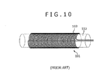
- FIG. 10 shows an example of a coil used in an existing position indicator disclosed in Patent Document 2 or the like.
- the coil 101 used in an existing position indicator is made by winding a conductive wire 103 around a ferrite core 102.
- the AC magnetic field transmitted from the coil 101 is detected by a sensor coil disposed in parallel relation to a tablet, thereby obtaining the indicated position.
- the AC voltage is applied to the coil 101, whereby the entire coil 101 acts as an electrode, thus generating an AC electric field.
- induced voltages due to the electrostatic induction are generated in each of plural lines of the sensor coil of the tablet.
- the resistance value of the sensor coil becomes as high as several kilo ohms to several tens of kilo ohms.
- the present invention is directed to providing a position indicator for use on a sensor coil having a high electrical resistance, whose indicated position is detected in accordance with an electromagnetic induction method, wherein an influence of the electrostatic induction between the position indicator and the sensor coil is excluded to thereby allow accurate detection of the indicated position.
- the present invention also provides a coil used in such a position indicator, a position detecting device used with such a position indicator, and a coil winding method.
- a coil including: a first conductive wire wound from a distal end portion thereof to a proximal end portion thereof in a predetermined rotational direction; and a second conductive wire wound from a proximal end portion thereof to a distal end portion thereof in the predetermined rotational direction; in which the first conductive wire and the second conductive wire are connected to each other at the proximal end portions thereof; and the wound first conductive wire and the wound second conductive wire are disposed alternately adjacent to each other.
- a position indicator including: an oscillation circuit configured to transmit a position indicating signal in order to indicate a position.
- the oscillation circuit includes a coil, which further includes a first conductive wire wound from a distal end portion thereof to a proximal end portion thereof in a predetermined rotational direction; and a second conductive wire wound from a proximal end portion thereof to a distal end portion thereof in the predetermined rotational direction; in which the first conductive wire and the second conductive wire are connected to each other at the proximal end portions thereof; and the wound first conductive wire and the wound second conductive wire are disposed alternately adjacent to each other.
- a position detecting device including: a position indicator including a coil for radiating a magnetic field for carrying out position indication; and a tablet including an input surface for receiving position indication made by the position indicator.
- the tablet is configured to detect a position indicated by the position indicator on the input surface in accordance with a magnetic field emitted from the position indicator.
- the coil includes a first conductive wire wound from a distal end portion thereof to a proximal end portion thereof in a predetermined rotational direction; and a second conductive wire wound from a proximal end portion thereof to a distal end portion thereof in the predetermined rotational direction.
- a position detecting device including: a position indicator including an oscillation circuit that includes a coil configured to emit a position indicating signal representing an indicated position; and a tablet including an input surface for receiving position indication made by the position indicator. Specifically, the tablet is configured to detect a position indicated by the position indicator on the input surface in accordance with a position indicating signal emitted from the position indicator.
- the coil includes a first conductive wire wound from a distal end portion thereof to a proximal end portion thereof in a predetermined rotational direction, and a second conductive wire wound from a proximal end portion thereof to a distal end portion thereof in the predetermined rotational direction, in which the first conductive wire and the second conductive wire are connected to each other at the proximal end portions thereof and the wound first conductive wire and the wound second conductive wire are disposed alternately adjacent to each other.
- the coil is configured to transmit the position indicating signal.
- a coil winding method including the steps of: designating a portion of a conductive wire from one predetermined point thereof to one end portion thereof as a first conductive wire, and designating another portion of the conductive wire from said one predetermined point to the other end portion thereof as a second conductive wire; fixing said one predetermined point of the conductive wire to a magnetic material having approximately a rod-like shape; winding the first conductive wire by a half turn in a first rotational direction, and winding the second conductive wire by a half turn in a second rotational direction, thereby placing the second conductive wire over the first conductive wire; and alternately winding the first conductive wire and the second conductive wire, for example along the last-wound conductive wire per each turn, to repetitively wind the first conductive wire and the second conductive wire by a predetermined number of turns. After the repetitive winding is completed, both end portions of the conductive wire are taken as both ends of the coil.
- the voltages which are opposite in polarity to each other and which have approximately the same potential are applied to the wound conductive wires that are adjacent to each other. For this reason, the electric fields generated from the conductive wires adjacent to each other cancel each other, and thus it is possible to suppress the radiation of the electric field from the coil.
- the sensor coil of the tablet can detect only the signal generated by the electromagnetic induction without being influenced by the electrostatic induction between the sensor coil and the position indicator. Thus, it is possible to precisely obtain the coordinates of the position indicator on the tablet.
- FIG. 1 shows a coil winding wire of a first embodiment of the present invention.
- a conductive wire 3 that forms a coil 1 has a predetermined length.
- a predetermined portion of the conductive wire 3 is determined as a middle point 4, and both end portions of the conductive wire 3 with respect to the middle point 4 are designated as a first end portion 5a and a second end portion 5b, respectively.
- a part of the conductive wire 3 extending from the middle point 4 to the first end portion 5a is designated as a first conductive wire 3a
- a part of the conductive wire 3 extending from the middle point 4 to the second end portion 5b is designated as a second conductive wire 3b.
- the first conductive wire 3a is wound from its one end portion (e.g., a distal end portion) to the other end portion (e.g., a proximal end portion near the middle point 4) in a predetermined rotational direction.
- the conductive wire 3 is folded back at the middle point 4 to be returned as the second conductive wire 3b back to the one end portion in the same rotational direction.
- the wound first conductive wire 3a and the wound second conductive wire 3b are disposed alternately adjacent to each other in respective portions of the coil 1.
- FIG. 2 shows a position indicator 10 having the coil 1 according to the first embodiment of the present invention.
- the position indicator 10 having the coil 1 includes a pen tip portion 10a, a pen holder 14b, the coil 1, a pen pressure sensor 12 for detecting a pen pressure applied to the pen tip portion 10a, and an oscillation circuit 13 (which cooperates with and functionally includes the coil 1).
- the coil 1 of the first embodiment is formed by using a special method of winding (knitting) the conductive wire 3 (refer to FIG. 7 , which will be described later) around the circumference of a ferrite core 2, and a winding process will be described later.
- the coil 1 and the ferrite core 2 are disposed close to the pen tip portion 10a.
- the pen tip portion 10a is provided at a distal end of a rod 11, which is inserted through a hole formed through the tip side of the pen holder 10b.
- the coil 1 is structured by winding a litz wire around the ferrite core 2, which includes a hole through which the rod 11 is slidably inserted.
- the coil 1 is disposed on the tip side of the pen holder 10b.
- the oscillation circuit 13, functionally including and cooperating with the coil 1, generates an AC signal, and transmits a position indicating signal to a tablet 31 (refer to FIG. 8 , which will be described later) via the coil 1.
- a battery may be used as a power source built in the position indicator 10.
- the power source which is charged by an excitation signal supplied thereto from the tablet 31 may also be used as the power source built in the position indicator 10.
- the pen pressure sensor 12 is composed of a variable capacitance capacitor, an example of which is disclosed in Japanese Patent Laid-Open No. Hei 5-275283 .
- an oscillation frequency may be changed in accordance with the pen pressure.
- the pen pressure may be converted into a binary code, and a signal generated in the coil 1 may be modulated by using the binary code.
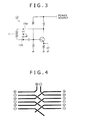
- FIG. 3 is a circuit diagram of a Colpitts type oscillation circuit used in the position indicator 10 having the coil 1 of the first embodiment.
- the oscillation circuit 13 of the position indicator 10 having the coil 1 of the first embodiment includes two capacitors 15a and 15b connected in series with each other, and the coil 1 connected in parallel with the two capacitors 15a and 15b, and is configured in the form of the well-known Colpitts type oscillation circuit.
- the two capacitors 15a and 15b are equal in electrostatic capacitance to each other, and a middle point to which each of the capacitors 15a and 15b is connected is connected to a predetermined fixed potential (a minus terminal of a power source (GND) in this case).
- the voltages generated in the coil 1 are as shown in FIG. 4 .
- the plus-side voltage and the minus-side voltage are alternately generated in each adjacent two winding wires of the coil 1, the electric fields radiated by each adjacent two winding wires cancel each other, to thus exert no influence to the surrounding. This is a feature of the present invention.
- the position indicator 10 includes the coil 1 in which the first and second conductive wires 3a and 3b are wound, from the starting end side and the terminating end side of the conductive wire 3, respectively, so as to be alternately adjacent to each other, per each turn. Therefore, the electric fields radiated from each adjacent two portions of the conductive wire 3 of the coil 1 cancel each other, to thereby reduce the radiation of the electric field from the coil 1.
- the Colpitts type oscillation circuit is used in the position indicator 10 having the coil 1 of the first embodiment, the signals which have the same amplitude and which are 180° out-of-phase with each other are generated at both ends of the conductive wire 3, respectively. Therefore, since the electric fields radiated by each adjacent two portions of the conductive wire 3 of the coil 1 fully cancel each other, it is possible to realize the position indicator which radiates very little electric field.
- the tablet 31 is free from the influence of the electrostatic induction between the positive indicator 10 and the sensor coil, and thus can precisely detect the indicated position indicated by the position indicator 10 on the sensor coil having a high electrical resistance.
- FIG. 5 is a view showing a coil winding wire of the coil 21.
- the coil 21 of the second embodiment is different from the coil 1 of the first embodiment in that in the coil 21, the middle point terminal 22 is drawn out from the middle point 4 of the conductive wire 3.
- FIG. 6 is a circuit diagram of a Hartley type oscillation circuit used in the position indicator 10 having the coil 21 of the second embodiment.
- one capacitor 23 is connected in parallel with the coil 21, to thereby form the well-known Hartley type oscillation circuit.
- a middle point terminal 22 connected to the middle point 4 of the coil 21 is connected to a predetermined fixed potential (a plus terminal of the power source (VCC) in this case).
- signals which have the same amplitude, with respect to the VCC potential as a reference, and which are 180° out-of-phase with each other are generated at both ends of the coil 21 or, more specifically, at both ends of the conductive wire 3 that forms the coil 21, respectively.
- the plus-side voltage and the minus-side voltage are alternately generated in each adjacent two winding wires of the coil 21.
- the position indicator 10 includes the coil 21 in which the first and second conductive wires 3a and 3b are wound, from the starting end side and the terminating end side of the conductive wire 3, respectively, so as to be alternately adjacent to each other, per each turn. Therefore, the electric fields radiated from each adjacent two portions of the conductive wire 3 of the coil 21 cancel each other, to thereby reduce the radiation of the electric field from the coil 21.
- the Hartley type oscillation circuit is used in the position indicator 10 having the coil 21 of the second embodiment, the signals which have the same amplitude, with respect to the potential at the middle point 22 as a reference, and which are 180° out-of-phase with each other are generated at both ends of the conductive wire 3, respectively. Thus, it is possible to realize the position indicator which radiates very little electric field because the electric fields radiated from each adjacent two portions of the conductive wire 3 of the coil 21 fully cancel each other.
- a resulting effect is that even when the sensor coil having a high electrical resistance is used in the tablet 31, the influence of the electrostatic induction between the position indicator 10 and the sensor coil is removed, and thus it is possible to precisely detect the indicated position of the position indicator 10 on the tablet 31.
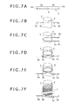
- FIGS. 7A to 7F are views explaining processes for manufacturing the coil 1 of the first embodiment shown in FIG. 1 .
- FIG. 7A shows a construction of the conductive wire 3.
- the conductive wire 3 in this case has a predetermined length, and both end portions of the conductive wire 3 with respect to the middle point 4 are designated as the first end portion 5a and the second end portion 5b, respectively. Also, a part of the conductive wire 3 extending from the middle point 4 to the first end portion 5a is designated as the first conductive wire 3a, and a part of the conductive wire 3 extending from the middle point 4 to the second end portion 5b is designated as the second conductive wire 3b.
- FIG. 7B shows a state in which the ferrite core 2 is placed over the middle point 4 of the conductive wire 3.
- the conductive wire 3 starts to be wound around the ferrite core 2 in a state shown in FIG. 7B .
- FIG. 7C shows a state in which the first conductive wire 3 a is wound around the ferrite core 2 by a half turn. At this time, the first conductive wire 3a is wound along the circumference of the ferrite core 2 by a half turn.
- FIG. 7D shows a state in which the second conductive wire 3b is wound around the ferrite core 2 by a half turn. At this time, the second conductive wire 3b is wound along the circumference of the ferrite core 2 by a half turn. Also, the second conductive wire 3b is placed on top of the first conductive wire 3a which has already been wound around the ferrite core 2 by a half turn.
- FIG. 7E shows a state in which the first conductive wire 3 a is wound around the ferrite core 2 by one more turn. At this time, the first conductive wire 3a is wound around the circumference of the ferrite core 2 by one turn so as to be adjacent to the second conductive wire 3b wound around the ferrite core 2 to be placed on top of the second conductive wire 3b.
- the second conductive wire 3b is placed on top of the first conductive wire 3 a.
- FIG . 7F shows the completed coil 1.
- the first end portion 5a and the second end portion 5b of the conductive wire 3 are taken and used as both ends of the coil 1.
- the conductive wire 3 is wound around the ferrite core 2 in the manner as described above, thereby forming the coil 1.
- the ferrite core 2 is used as the core of the coil 1, 21, any other suitable material may be used instead of using the ferrite core 2.
- the fixing portion (provided by the ferrite core 2, for example) may be removed from the coil 1, 21, thereby obtaining a hollow core coil.
- the NPN bipolar transistor is used as the constituent element composing the oscillation circuit 13, the present invention is by no means limited thereto.
- a single wire may be used as the conductive wire 3 which is wound around the ferrite core 2 in order to obtain the coil 1, 21, or a plurality of fine conductive wires may be bundled for use in formation of the coil 1, 21.
- first conductive wire 3a and the second conductive wire 3b are alternately wound around the ferrite core 2 so as to be adjacent to each other per each turn
- first conductive wire 3a and the second conductive wire 3b may be alternately wound around the ferrite core 2 so as to be adjacent to each other per every two turns or more turns.
- FIG. 8 shows a position detecting device (hereinafter referred to as "a pen tablet") 30, according to a third embodiment of the present invention, including the position indicator 10 having the construction and operation as described above.
- a pen tablet a position detecting device
- the pen tablet 30 has the pen-shaped position indicator 10, and a flat plate-like tablet 31.
- the pen-shaped position indicator 10 has the pen tip portion 10a, and the coil 1 is accommodated in the pen tip portion 10a.
- the tablet 31 is connected to an external computer apparatus (not shown), and has a function of detecting an indicated position indicated by the position indicator 10.
- the position indicator 10 is used on a position detection area 31a set on an upper surface of the tablet 31.
- the tablet 31 can detect a coordinate position which is indicated on the position detection area 31 a by the position indicator 10.
- Information regarding the indicated position indicated by the position indicator 10 and detected by the tablet 31 is outputted to the external computer apparatus.
- the external computer apparatus displays a drawing or the like corresponding to the coordinates inputted thereto from the tablet 31 on a screen of a liquid crystal display device (not shown) connected thereto.
- FIG. 9 is a block diagram showing a configuration of the tablet 31.
- the tablet 31 includes a plurality of loop coils 41.
- a plurality of loop coils 41 are composed of loop coils X1 to X20 which are disposed in an X-axis direction approximately in parallel with one another (hereinafter referred to as "X-axis loop coils”), and loop coils Y1 to Y20 which are disposed in a Y-axis direction approximately in parallel with one another (hereinafter referred to as "Y-axis loop coils”),
- the dimensions and pitch of the plurality of loop coils 41, of the position detection area 31a, composed of the X-axis loop coils X1 to X20 and the Y-axis loop coils Y1 to Y20, are determined according to the size of the tablet 31.
- the plurality of loop coils 41 receive the position indicating signal representing the indicated position indicated by the position indicator 10 from the position indicator 10 placed on the position detection area 31 a.
- a plurality of loop coils 41 composed of the X-axis loop coils X1 to X20 and the Y-axis loop coils Y1 to Y20 are connected to a selecting circuit 42 for selecting a set of output terminals of the X-axis loop coil and the Y-axis loop coil which correspond to the indicated position on the position detection area 31a.
- a set of output terminals of the X-axis loop coil and the Y-axis loop coil which is selected by the selecting circuit 42 is connected to an amplifying circuit 43.
- the amplifying circuit 43 is connected to a band-pass filter 44 having a frequency fo, which is the frequency of the signal from the position indicator 10, as a central frequency.
- the band-pass filter 44 is connected to a detector circuit 45.
- the detector circuit 45 is connected to a sample-and-hold circuit 46.
- a voltage held by the sample-and-hold circuit 46 is converted from an analog signal into a digital signal in an A/D conversion circuit 47.
- the digital signal outputted from the A/D conversion circuit 47 is inputted to a CPU 48.
- the CPU 48 sends control signals to the selecting circuit 42, the sample-and-hold circuit 46, and the A/D conversion circuit 47, respectively, and obtains the indicated position indicated by the position indicator 10 in the position detection area 31 a in accordance with the position indicating signal received by corresponding ones of the X-axis loop coils X1 to X20 and the Y-axis loop coils Y1 to Y20 that form the loop coils 41.
- the CPU 48 when there is no position indicator 10 on the tablet 31, the CPU 48 carries out the scanning for the entire tablet 31. Specifically, while the X-axis loop coils X1 to X20 and the Y-axis loop coils Y1 to Y20 are successively selected in the order from X1 to X20 and in the order from Y1 to Y20, respectively, on a one-by-one basis by the selecting circuit 22, the CPU 48 detects the presence or absence of, and the level of, each of the output signals from the X-axis loop coils X1 to X20 and the Y-axis loop coils Y1 to Y20, which are selected on the one-by-one basis, through the amplifying circuit 43, the detector circuit 45, the sample-and-hold circuit 46, and the A/D conversion circuit 47.
- the signals are detected from the corresponding ones of the X-axis loop coils X1 to X20 and the Y-axis loop coils Y1 to Y20 in the vicinity of the position indicator 10.
- the operation of the CPU 48 proceeds to the scanning of only several (about 5 to about 7) loop coils 41, which is centered around the loop coil from which the strongest signal was detected, with respect to both the X-axis loop coils and the Y-axis loop coils, respectively.
- the operation of the CPU 48 described above is carried out for both the X-axis loop coils X1 to X20 and the Y-axis loop coils Y1 to Y20 forming the loop coils 41, and thus the results of detection of the levels of the signals from the X-axis loop coils X1 to X20 and the Y-axis loop coils Y1 to Y20 show a two-dimensional distribution.
- the position of the position indicator 10 on the pen tablet 30 is detected in accordance with the distribution of the levels of the signals.
- a position detecting device includes: the position indicator 10 including the coil 1 for radiating the magnetic field for carrying out the position indication; and the tablet 31 including the position detection area 31a for receiving position indication made by the position indicator 10.
- the tablet 31 serves to detect the position indicated by the position indicator 10 on the position detection area 31a in accordance with the magnetic field emitted from the position indicator 10.
- the coil 1 includes: the first conductive wire 3a wound from a distal end portion thereof to a proximal end portion thereof in a predetermined rotational direction; and the second conductive wire 3b wound from a proximal end portion thereof to a distal end portion thereof in the predetermined rotational direction.
- position indicator 10 and the coil winding method of the present invention are embodied as described in the coils 1 and 21 of the first and second embodiments of the present invention.
- the oscillation circuit is by no means limited to the Colpitts type oscillation circuit and the Hartley type oscillation circuit.
Landscapes
- Engineering & Computer Science (AREA)
- Power Engineering (AREA)
- Theoretical Computer Science (AREA)
- General Engineering & Computer Science (AREA)
- Physics & Mathematics (AREA)
- Human Computer Interaction (AREA)
- General Physics & Mathematics (AREA)
- Manufacturing & Machinery (AREA)
- Electromagnetism (AREA)
- Position Input By Displaying (AREA)
- Measurement Of Length, Angles, Or The Like Using Electric Or Magnetic Means (AREA)
- Coil Winding Methods And Apparatuses (AREA)
- Coils Or Transformers For Communication (AREA)
Applications Claiming Priority (1)
| Application Number | Priority Date | Filing Date | Title |
|---|---|---|---|
| JP2009262296A JP5275959B2 (ja) | 2009-11-17 | 2009-11-17 | コイル、位置指示器、位置検出装置及びコイル巻回方法 |
Publications (3)
| Publication Number | Publication Date |
|---|---|
| EP2323140A2 true EP2323140A2 (de) | 2011-05-18 |
| EP2323140A3 EP2323140A3 (de) | 2014-03-19 |
| EP2323140B1 EP2323140B1 (de) | 2018-05-30 |
Family
ID=43607845
Family Applications (1)
| Application Number | Title | Priority Date | Filing Date |
|---|---|---|---|
| EP10191525.4A Not-in-force EP2323140B1 (de) | 2009-11-17 | 2010-11-17 | Positionsanzeiger, positionserkennungsvorrichtung und spulenwickelverfahren |
Country Status (5)
| Country | Link |
|---|---|
| US (1) | US8847928B2 (de) |
| EP (1) | EP2323140B1 (de) |
| JP (1) | JP5275959B2 (de) |
| CN (1) | CN102063237A (de) |
| TW (1) | TWI476794B (de) |
Cited By (3)
| Publication number | Priority date | Publication date | Assignee | Title |
|---|---|---|---|---|
| CN105829997A (zh) * | 2013-12-25 | 2016-08-03 | 株式会社和冠 | 位置指示用模块及触控笔 |
| EP2637082A3 (de) * | 2012-03-09 | 2017-08-02 | Wacom Co., Ltd. | Sensor für Koordinateneingabevorrichtung mit elektromagnetischer Induktion |
| CN115136106A (zh) * | 2020-03-12 | 2022-09-30 | 株式会社和冠 | 位置检测传感器及位置检测传感器的制造方法 |
Families Citing this family (16)
| Publication number | Priority date | Publication date | Assignee | Title |
|---|---|---|---|---|
| JP5430339B2 (ja) * | 2009-10-19 | 2014-02-26 | 株式会社ワコム | 位置検出装置及び位置指示器 |
| CN103019498A (zh) * | 2011-09-20 | 2013-04-03 | 友碁科技股份有限公司 | 电磁感应式输入设备 |
| US8878824B2 (en) | 2012-04-11 | 2014-11-04 | Blackberry Limited | Force-sensing stylus pointing device |
| JP5954115B2 (ja) * | 2012-10-26 | 2016-07-20 | Tdk株式会社 | 電子ペン用コイル装置 |
| CN103823579B (zh) * | 2012-11-15 | 2017-01-04 | Tdk株式会社 | 电子笔用线圈装置 |
| JP6032016B2 (ja) * | 2013-01-10 | 2016-11-24 | Tdk株式会社 | 電子ペン用コイル装置 |
| KR102065703B1 (ko) | 2013-02-07 | 2020-02-11 | 삼성전자주식회사 | 터치 펜, 터치 펜 인식을 위한 전자 장치 및 그 운용 방법 |
| WO2015106117A1 (en) * | 2014-01-09 | 2015-07-16 | Minipumps, Llc | Telemetry arrangements for implantable devices |
| WO2016022713A1 (en) * | 2014-08-05 | 2016-02-11 | Purvis Rick | Telemetry arrangements for implantable devices |
| DE102015216010A1 (de) * | 2015-08-21 | 2017-02-23 | Robert Bosch Gmbh | Magnetspule mit einem Wicklungsträger und Verfahren zum Aufbringen einer Wicklung |
| JP6037492B1 (ja) * | 2016-06-24 | 2016-12-07 | 株式会社ワコム | 発信型電子ペンの信号発信回路及び発信型電子ペン |
| JP6750488B2 (ja) * | 2016-12-02 | 2020-09-02 | スミダコーポレーション株式会社 | アンテナ装置およびその製造方法 |
| WO2018159333A1 (ja) * | 2017-02-28 | 2018-09-07 | 日本電産リード株式会社 | コイル状電子部品、コイル部品、コイル部品の製造方法、インダクタンス素子、t型フィルタ、発振回路、及びインダクタンス素子の製造方法 |
| US20180294708A1 (en) * | 2017-04-06 | 2018-10-11 | Bryan Healey Sample | Power source for portable electronic device |
| KR102360971B1 (ko) * | 2019-02-14 | 2022-02-09 | 주식회사 하이딥 | 스타일러스 펜 |
| JP7569577B2 (ja) | 2022-06-16 | 2024-10-18 | 株式会社 ハイディープ | ペン及びタッチ入力システム及びコントローラ |
Family Cites Families (18)
| Publication number | Priority date | Publication date | Assignee | Title |
|---|---|---|---|---|
| US4571557A (en) * | 1984-03-26 | 1986-02-18 | Randy Brandt | Wide band transistor oscillator |
| JPS6370326A (ja) * | 1986-09-12 | 1988-03-30 | Wacom Co Ltd | 位置検出装置 |
| US5061891A (en) * | 1988-11-21 | 1991-10-29 | Yazaki Corporation | Cross coil |
| DE69011292T2 (de) * | 1989-07-03 | 1995-03-16 | Sokymat S A | Verfahren zur herstellung von elektronischen komponenten mit einer spule aus dünndraht. |
| JP3071553B2 (ja) | 1992-03-24 | 2000-07-31 | 株式会社ワコム | 可変容量コンデンサ及びこれを利用した位置指示器 |
| JP3135183B2 (ja) | 1993-10-29 | 2001-02-13 | 株式会社ワコム | 位置指示器 |
| US5565836A (en) * | 1994-12-20 | 1996-10-15 | The United States Of America As Represented By The Secretary Of The Army | Nullification of magnetic fields relative to coils |
| JP3169314B2 (ja) * | 1995-01-20 | 2001-05-21 | 日特エンジニアリング株式会社 | 多層コイルおよびその巻線方法 |
| US5640970A (en) * | 1995-04-26 | 1997-06-24 | Cordis Corporation | Guidewire having a controlled radiopacity tip |
| US5579887A (en) * | 1995-06-15 | 1996-12-03 | Coin Acceptors, Inc. | Coin detection apparatus |
| JP3525971B2 (ja) | 1996-02-14 | 2004-05-10 | 日特エンジニアリング株式会社 | コイルボビン用巻線機 |
| JP3324584B2 (ja) | 1999-10-20 | 2002-09-17 | 松下電器産業株式会社 | 放電灯の製造方法 |
| US6834251B1 (en) * | 2001-12-06 | 2004-12-21 | Richard Fletcher | Methods and devices for identifying, sensing and tracking objects over a surface |
| JP2006065757A (ja) | 2004-08-30 | 2006-03-09 | Wacom Co Ltd | 座標指示器 |
| US20080128180A1 (en) * | 2004-12-01 | 2008-06-05 | Haim Perski | Position Detecting System and Apparatuses and Methods For Use and Control Thereof |
| JP4751191B2 (ja) | 2005-12-12 | 2011-08-17 | 株式会社ワコム | 位置検出器、及び、位置入力装置 |
| JP4709674B2 (ja) * | 2006-03-23 | 2011-06-22 | 株式会社ワコム | 位置検出装置及びコンピュータ |
| JP5109171B2 (ja) * | 2007-09-18 | 2012-12-26 | 株式会社ワコム | 位置指示器、位置入力装置及びコンピュータシステム |
-
2009
- 2009-11-17 JP JP2009262296A patent/JP5275959B2/ja not_active Expired - Fee Related
-
2010
- 2010-10-26 US US12/912,092 patent/US8847928B2/en not_active Expired - Fee Related
- 2010-11-05 TW TW099138181A patent/TWI476794B/zh not_active IP Right Cessation
- 2010-11-17 EP EP10191525.4A patent/EP2323140B1/de not_active Not-in-force
- 2010-11-17 CN CN2010105511734A patent/CN102063237A/zh active Pending
Cited By (4)
| Publication number | Priority date | Publication date | Assignee | Title |
|---|---|---|---|---|
| EP2637082A3 (de) * | 2012-03-09 | 2017-08-02 | Wacom Co., Ltd. | Sensor für Koordinateneingabevorrichtung mit elektromagnetischer Induktion |
| CN105829997A (zh) * | 2013-12-25 | 2016-08-03 | 株式会社和冠 | 位置指示用模块及触控笔 |
| CN105829997B (zh) * | 2013-12-25 | 2019-05-17 | 株式会社和冠 | 位置指示用模块及触控笔 |
| CN115136106A (zh) * | 2020-03-12 | 2022-09-30 | 株式会社和冠 | 位置检测传感器及位置检测传感器的制造方法 |
Also Published As
| Publication number | Publication date |
|---|---|
| US8847928B2 (en) | 2014-09-30 |
| US20110115753A1 (en) | 2011-05-19 |
| TWI476794B (zh) | 2015-03-11 |
| TW201142883A (en) | 2011-12-01 |
| JP5275959B2 (ja) | 2013-08-28 |
| JP2011107985A (ja) | 2011-06-02 |
| CN102063237A (zh) | 2011-05-18 |
| EP2323140A3 (de) | 2014-03-19 |
| EP2323140B1 (de) | 2018-05-30 |
Similar Documents
| Publication | Publication Date | Title |
|---|---|---|
| US8847928B2 (en) | Coil, position indicator, position detecting device, and coil winding method | |
| US11983357B2 (en) | Electronic device, stylus pen, and method for driving and controlling same | |
| JP6021174B2 (ja) | 位置検出装置およびその位置指示器 | |
| JP5430339B2 (ja) | 位置検出装置及び位置指示器 | |
| US9778761B2 (en) | Capacitive stylus pen | |
| EP2187288B1 (de) | Positionsanzeiger, variabler Kondensator und Eingabegerät | |
| CN107111399B (zh) | 位置指示器 | |
| JP2011065450A (ja) | 位置検出装置及び位置指示器 | |
| CN103699288B (zh) | 电磁感应方式的位置检测传感器 | |
| KR102198176B1 (ko) | 좌표 표시 장치의 주파수 측정 방법 및 그에 따른 전자기기 | |
| TWI643100B (zh) | Position detecting device and its position indicator | |
| TWI554935B (zh) | Electromagnetic induction input device | |
| JP5852631B2 (ja) | 位置指示器 | |
| KR102366071B1 (ko) | 검출 장치, 입력 장치 및 검출 방법 | |
| CN104516617A (zh) | 触摸输入设备 | |
| JP2010055385A (ja) | 複数の指示具を識別可能なデジタイザ | |
| CN1087850C (zh) | 无绳数字变换器 | |
| TWM421545U (en) | Electromagnetic induction type input device | |
| KR101522701B1 (ko) | 비접촉식 광학렌즈 2차원 위치 탐지 시스템 | |
| US10025398B2 (en) | Position measurement device for measuring position of pen and method for controlling same | |
| KR101551869B1 (ko) | 비접촉식 광학렌즈 높이 탐지 시스템 | |
| JPH07111672B2 (ja) | 位置検出装置 | |
| JPH07111673B2 (ja) | 位置検出装置 |
Legal Events
| Date | Code | Title | Description |
|---|---|---|---|
| PUAI | Public reference made under article 153(3) epc to a published international application that has entered the european phase |
Free format text: ORIGINAL CODE: 0009012 |
|
| AK | Designated contracting states |
Kind code of ref document: A2 Designated state(s): AL AT BE BG CH CY CZ DE DK EE ES FI FR GB GR HR HU IE IS IT LI LT LU LV MC MK MT NL NO PL PT RO RS SE SI SK SM TR |
|
| AX | Request for extension of the european patent |
Extension state: BA ME |
|
| PUAL | Search report despatched |
Free format text: ORIGINAL CODE: 0009013 |
|
| AK | Designated contracting states |
Kind code of ref document: A3 Designated state(s): AL AT BE BG CH CY CZ DE DK EE ES FI FR GB GR HR HU IE IS IT LI LT LU LV MC MK MT NL NO PL PT RO RS SE SI SK SM TR |
|
| AX | Request for extension of the european patent |
Extension state: BA ME |
|
| RIC1 | Information provided on ipc code assigned before grant |
Ipc: H01Q 7/08 20060101ALI20140212BHEP Ipc: G06F 3/041 20060101ALI20140212BHEP Ipc: H01F 41/06 20060101ALI20140212BHEP Ipc: H01F 5/00 20060101AFI20140212BHEP |
|
| 17P | Request for examination filed |
Effective date: 20140916 |
|
| RBV | Designated contracting states (corrected) |
Designated state(s): AL AT BE BG CH CY CZ DE DK EE ES FI FR GB GR HR HU IE IS IT LI LT LU LV MC MK MT NL NO PL PT RO RS SE SI SK SM TR |
|
| 17Q | First examination report despatched |
Effective date: 20170215 |
|
| REG | Reference to a national code |
Ref country code: DE Ref legal event code: R079 Ref document number: 602010050887 Country of ref document: DE Free format text: PREVIOUS MAIN CLASS: H01F0005000000 Ipc: H01F0041064000 |
|
| GRAP | Despatch of communication of intention to grant a patent |
Free format text: ORIGINAL CODE: EPIDOSNIGR1 |
|
| RIC1 | Information provided on ipc code assigned before grant |
Ipc: H01F 41/071 20160101ALI20180124BHEP Ipc: G06F 3/0354 20130101ALI20180124BHEP Ipc: G06F 3/046 20060101ALI20180124BHEP Ipc: H01Q 7/08 20060101ALI20180124BHEP Ipc: H01F 41/064 20160101AFI20180124BHEP Ipc: H01F 5/00 20060101ALI20180124BHEP |
|
| INTG | Intention to grant announced |
Effective date: 20180208 |
|
| RIN1 | Information on inventor provided before grant (corrected) |
Inventor name: KATSURAHIRA, YUJI |
|
| GRAS | Grant fee paid |
Free format text: ORIGINAL CODE: EPIDOSNIGR3 |
|
| GRAA | (expected) grant |
Free format text: ORIGINAL CODE: 0009210 |
|
| AK | Designated contracting states |
Kind code of ref document: B1 Designated state(s): AL AT BE BG CH CY CZ DE DK EE ES FI FR GB GR HR HU IE IS IT LI LT LU LV MC MK MT NL NO PL PT RO RS SE SI SK SM TR |
|
| REG | Reference to a national code |
Ref country code: GB Ref legal event code: FG4D |
|
| REG | Reference to a national code |
Ref country code: CH Ref legal event code: EP |
|
| REG | Reference to a national code |
Ref country code: AT Ref legal event code: REF Ref document number: 1004454 Country of ref document: AT Kind code of ref document: T Effective date: 20180615 |
|
| REG | Reference to a national code |
Ref country code: IE Ref legal event code: FG4D |
|
| REG | Reference to a national code |
Ref country code: DE Ref legal event code: R096 Ref document number: 602010050887 Country of ref document: DE |
|
| REG | Reference to a national code |
Ref country code: NL Ref legal event code: MP Effective date: 20180530 |
|
| REG | Reference to a national code |
Ref country code: LT Ref legal event code: MG4D |
|
| PG25 | Lapsed in a contracting state [announced via postgrant information from national office to epo] |
Ref country code: CY Free format text: LAPSE BECAUSE OF FAILURE TO SUBMIT A TRANSLATION OF THE DESCRIPTION OR TO PAY THE FEE WITHIN THE PRESCRIBED TIME-LIMIT Effective date: 20180530 Ref country code: LT Free format text: LAPSE BECAUSE OF FAILURE TO SUBMIT A TRANSLATION OF THE DESCRIPTION OR TO PAY THE FEE WITHIN THE PRESCRIBED TIME-LIMIT Effective date: 20180530 Ref country code: NO Free format text: LAPSE BECAUSE OF FAILURE TO SUBMIT A TRANSLATION OF THE DESCRIPTION OR TO PAY THE FEE WITHIN THE PRESCRIBED TIME-LIMIT Effective date: 20180830 Ref country code: SE Free format text: LAPSE BECAUSE OF FAILURE TO SUBMIT A TRANSLATION OF THE DESCRIPTION OR TO PAY THE FEE WITHIN THE PRESCRIBED TIME-LIMIT Effective date: 20180530 Ref country code: ES Free format text: LAPSE BECAUSE OF FAILURE TO SUBMIT A TRANSLATION OF THE DESCRIPTION OR TO PAY THE FEE WITHIN THE PRESCRIBED TIME-LIMIT Effective date: 20180530 Ref country code: FI Free format text: LAPSE BECAUSE OF FAILURE TO SUBMIT A TRANSLATION OF THE DESCRIPTION OR TO PAY THE FEE WITHIN THE PRESCRIBED TIME-LIMIT Effective date: 20180530 Ref country code: BG Free format text: LAPSE BECAUSE OF FAILURE TO SUBMIT A TRANSLATION OF THE DESCRIPTION OR TO PAY THE FEE WITHIN THE PRESCRIBED TIME-LIMIT Effective date: 20180830 |
|
| PG25 | Lapsed in a contracting state [announced via postgrant information from national office to epo] |
Ref country code: RS Free format text: LAPSE BECAUSE OF FAILURE TO SUBMIT A TRANSLATION OF THE DESCRIPTION OR TO PAY THE FEE WITHIN THE PRESCRIBED TIME-LIMIT Effective date: 20180530 Ref country code: GR Free format text: LAPSE BECAUSE OF FAILURE TO SUBMIT A TRANSLATION OF THE DESCRIPTION OR TO PAY THE FEE WITHIN THE PRESCRIBED TIME-LIMIT Effective date: 20180831 Ref country code: LV Free format text: LAPSE BECAUSE OF FAILURE TO SUBMIT A TRANSLATION OF THE DESCRIPTION OR TO PAY THE FEE WITHIN THE PRESCRIBED TIME-LIMIT Effective date: 20180530 Ref country code: HR Free format text: LAPSE BECAUSE OF FAILURE TO SUBMIT A TRANSLATION OF THE DESCRIPTION OR TO PAY THE FEE WITHIN THE PRESCRIBED TIME-LIMIT Effective date: 20180530 |
|
| REG | Reference to a national code |
Ref country code: AT Ref legal event code: MK05 Ref document number: 1004454 Country of ref document: AT Kind code of ref document: T Effective date: 20180530 |
|
| PG25 | Lapsed in a contracting state [announced via postgrant information from national office to epo] |
Ref country code: NL Free format text: LAPSE BECAUSE OF FAILURE TO SUBMIT A TRANSLATION OF THE DESCRIPTION OR TO PAY THE FEE WITHIN THE PRESCRIBED TIME-LIMIT Effective date: 20180530 |
|
| PG25 | Lapsed in a contracting state [announced via postgrant information from national office to epo] |
Ref country code: DK Free format text: LAPSE BECAUSE OF FAILURE TO SUBMIT A TRANSLATION OF THE DESCRIPTION OR TO PAY THE FEE WITHIN THE PRESCRIBED TIME-LIMIT Effective date: 20180530 Ref country code: PL Free format text: LAPSE BECAUSE OF FAILURE TO SUBMIT A TRANSLATION OF THE DESCRIPTION OR TO PAY THE FEE WITHIN THE PRESCRIBED TIME-LIMIT Effective date: 20180530 Ref country code: AT Free format text: LAPSE BECAUSE OF FAILURE TO SUBMIT A TRANSLATION OF THE DESCRIPTION OR TO PAY THE FEE WITHIN THE PRESCRIBED TIME-LIMIT Effective date: 20180530 Ref country code: EE Free format text: LAPSE BECAUSE OF FAILURE TO SUBMIT A TRANSLATION OF THE DESCRIPTION OR TO PAY THE FEE WITHIN THE PRESCRIBED TIME-LIMIT Effective date: 20180530 Ref country code: RO Free format text: LAPSE BECAUSE OF FAILURE TO SUBMIT A TRANSLATION OF THE DESCRIPTION OR TO PAY THE FEE WITHIN THE PRESCRIBED TIME-LIMIT Effective date: 20180530 Ref country code: SK Free format text: LAPSE BECAUSE OF FAILURE TO SUBMIT A TRANSLATION OF THE DESCRIPTION OR TO PAY THE FEE WITHIN THE PRESCRIBED TIME-LIMIT Effective date: 20180530 Ref country code: CZ Free format text: LAPSE BECAUSE OF FAILURE TO SUBMIT A TRANSLATION OF THE DESCRIPTION OR TO PAY THE FEE WITHIN THE PRESCRIBED TIME-LIMIT Effective date: 20180530 |
|
| REG | Reference to a national code |
Ref country code: CH Ref legal event code: PK Free format text: BERICHTIGUNGEN |
|
| RIC2 | Information provided on ipc code assigned after grant |
Ipc: H01F 41/064 20160101AFI20180124BHEP Ipc: H01Q 7/08 20060101ALI20180124BHEP Ipc: H01F 5/00 20060101ALI20180124BHEP Ipc: G06F 3/0354 20130101ALI20180124BHEP Ipc: G06F 3/046 20060101ALI20180124BHEP Ipc: H01F 41/071 20160101ALI20180124BHEP |
|
| PG25 | Lapsed in a contracting state [announced via postgrant information from national office to epo] |
Ref country code: IT Free format text: LAPSE BECAUSE OF FAILURE TO SUBMIT A TRANSLATION OF THE DESCRIPTION OR TO PAY THE FEE WITHIN THE PRESCRIBED TIME-LIMIT Effective date: 20180530 Ref country code: SM Free format text: LAPSE BECAUSE OF FAILURE TO SUBMIT A TRANSLATION OF THE DESCRIPTION OR TO PAY THE FEE WITHIN THE PRESCRIBED TIME-LIMIT Effective date: 20180530 |
|
| REG | Reference to a national code |
Ref country code: DE Ref legal event code: R097 Ref document number: 602010050887 Country of ref document: DE |
|
| PLBE | No opposition filed within time limit |
Free format text: ORIGINAL CODE: 0009261 |
|
| STAA | Information on the status of an ep patent application or granted ep patent |
Free format text: STATUS: NO OPPOSITION FILED WITHIN TIME LIMIT |
|
| 26N | No opposition filed |
Effective date: 20190301 |
|
| PG25 | Lapsed in a contracting state [announced via postgrant information from national office to epo] |
Ref country code: SI Free format text: LAPSE BECAUSE OF FAILURE TO SUBMIT A TRANSLATION OF THE DESCRIPTION OR TO PAY THE FEE WITHIN THE PRESCRIBED TIME-LIMIT Effective date: 20180530 |
|
| REG | Reference to a national code |
Ref country code: CH Ref legal event code: PL |
|
| PG25 | Lapsed in a contracting state [announced via postgrant information from national office to epo] |
Ref country code: LU Free format text: LAPSE BECAUSE OF NON-PAYMENT OF DUE FEES Effective date: 20181117 Ref country code: MC Free format text: LAPSE BECAUSE OF FAILURE TO SUBMIT A TRANSLATION OF THE DESCRIPTION OR TO PAY THE FEE WITHIN THE PRESCRIBED TIME-LIMIT Effective date: 20180530 |
|
| REG | Reference to a national code |
Ref country code: BE Ref legal event code: MM Effective date: 20181130 |
|
| REG | Reference to a national code |
Ref country code: IE Ref legal event code: MM4A |
|
| PG25 | Lapsed in a contracting state [announced via postgrant information from national office to epo] |
Ref country code: CH Free format text: LAPSE BECAUSE OF NON-PAYMENT OF DUE FEES Effective date: 20181130 Ref country code: LI Free format text: LAPSE BECAUSE OF NON-PAYMENT OF DUE FEES Effective date: 20181130 |
|
| PG25 | Lapsed in a contracting state [announced via postgrant information from national office to epo] |
Ref country code: IE Free format text: LAPSE BECAUSE OF NON-PAYMENT OF DUE FEES Effective date: 20181117 Ref country code: FR Free format text: LAPSE BECAUSE OF NON-PAYMENT OF DUE FEES Effective date: 20181130 |
|
| PG25 | Lapsed in a contracting state [announced via postgrant information from national office to epo] |
Ref country code: BE Free format text: LAPSE BECAUSE OF NON-PAYMENT OF DUE FEES Effective date: 20181130 Ref country code: AL Free format text: LAPSE BECAUSE OF FAILURE TO SUBMIT A TRANSLATION OF THE DESCRIPTION OR TO PAY THE FEE WITHIN THE PRESCRIBED TIME-LIMIT Effective date: 20180530 |
|
| PG25 | Lapsed in a contracting state [announced via postgrant information from national office to epo] |
Ref country code: MT Free format text: LAPSE BECAUSE OF NON-PAYMENT OF DUE FEES Effective date: 20181117 |
|
| PG25 | Lapsed in a contracting state [announced via postgrant information from national office to epo] |
Ref country code: TR Free format text: LAPSE BECAUSE OF FAILURE TO SUBMIT A TRANSLATION OF THE DESCRIPTION OR TO PAY THE FEE WITHIN THE PRESCRIBED TIME-LIMIT Effective date: 20180530 |
|
| PG25 | Lapsed in a contracting state [announced via postgrant information from national office to epo] |
Ref country code: PT Free format text: LAPSE BECAUSE OF FAILURE TO SUBMIT A TRANSLATION OF THE DESCRIPTION OR TO PAY THE FEE WITHIN THE PRESCRIBED TIME-LIMIT Effective date: 20180530 |
|
| PG25 | Lapsed in a contracting state [announced via postgrant information from national office to epo] |
Ref country code: HU Free format text: LAPSE BECAUSE OF FAILURE TO SUBMIT A TRANSLATION OF THE DESCRIPTION OR TO PAY THE FEE WITHIN THE PRESCRIBED TIME-LIMIT; INVALID AB INITIO Effective date: 20101117 Ref country code: MK Free format text: LAPSE BECAUSE OF NON-PAYMENT OF DUE FEES Effective date: 20180530 |
|
| PG25 | Lapsed in a contracting state [announced via postgrant information from national office to epo] |
Ref country code: IS Free format text: LAPSE BECAUSE OF FAILURE TO SUBMIT A TRANSLATION OF THE DESCRIPTION OR TO PAY THE FEE WITHIN THE PRESCRIBED TIME-LIMIT Effective date: 20180930 |
|
| PGFP | Annual fee paid to national office [announced via postgrant information from national office to epo] |
Ref country code: DE Payment date: 20201119 Year of fee payment: 11 Ref country code: GB Payment date: 20201119 Year of fee payment: 11 |
|
| REG | Reference to a national code |
Ref country code: DE Ref legal event code: R119 Ref document number: 602010050887 Country of ref document: DE |
|
| GBPC | Gb: european patent ceased through non-payment of renewal fee |
Effective date: 20211117 |
|
| PG25 | Lapsed in a contracting state [announced via postgrant information from national office to epo] |
Ref country code: GB Free format text: LAPSE BECAUSE OF NON-PAYMENT OF DUE FEES Effective date: 20211117 Ref country code: DE Free format text: LAPSE BECAUSE OF NON-PAYMENT OF DUE FEES Effective date: 20220601 |