EP2320433A1 - Photosensitive conductive film, method for forming conductive film, method for forming conductive pattern, and conductive film substrate - Google Patents
Photosensitive conductive film, method for forming conductive film, method for forming conductive pattern, and conductive film substrate Download PDFInfo
- Publication number
- EP2320433A1 EP2320433A1 EP09808160A EP09808160A EP2320433A1 EP 2320433 A1 EP2320433 A1 EP 2320433A1 EP 09808160 A EP09808160 A EP 09808160A EP 09808160 A EP09808160 A EP 09808160A EP 2320433 A1 EP2320433 A1 EP 2320433A1
- Authority
- EP
- European Patent Office
- Prior art keywords
- conductive
- substrate
- conductive film
- photosensitive
- film
- Prior art date
- Legal status (The legal status is an assumption and is not a legal conclusion. Google has not performed a legal analysis and makes no representation as to the accuracy of the status listed.)
- Granted
Links
Images

Classifications
-
- G—PHYSICS
- G02—OPTICS
- G02F—OPTICAL DEVICES OR ARRANGEMENTS FOR THE CONTROL OF LIGHT BY MODIFICATION OF THE OPTICAL PROPERTIES OF THE MEDIA OF THE ELEMENTS INVOLVED THEREIN; NON-LINEAR OPTICS; FREQUENCY-CHANGING OF LIGHT; OPTICAL LOGIC ELEMENTS; OPTICAL ANALOGUE/DIGITAL CONVERTERS
- G02F1/00—Devices or arrangements for the control of the intensity, colour, phase, polarisation or direction of light arriving from an independent light source, e.g. switching, gating or modulating; Non-linear optics
- G02F1/01—Devices or arrangements for the control of the intensity, colour, phase, polarisation or direction of light arriving from an independent light source, e.g. switching, gating or modulating; Non-linear optics for the control of the intensity, phase, polarisation or colour
- G02F1/13—Devices or arrangements for the control of the intensity, colour, phase, polarisation or direction of light arriving from an independent light source, e.g. switching, gating or modulating; Non-linear optics for the control of the intensity, phase, polarisation or colour based on liquid crystals, e.g. single liquid crystal display cells
- G02F1/133—Constructional arrangements; Operation of liquid crystal cells; Circuit arrangements
- G02F1/1333—Constructional arrangements; Manufacturing methods
- G02F1/1343—Electrodes
- G02F1/13439—Electrodes characterised by their electrical, optical, physical properties; materials therefor; method of making
-
- H—ELECTRICITY
- H01—ELECTRIC ELEMENTS
- H01B—CABLES; CONDUCTORS; INSULATORS; SELECTION OF MATERIALS FOR THEIR CONDUCTIVE, INSULATING OR DIELECTRIC PROPERTIES
- H01B5/00—Non-insulated conductors or conductive bodies characterised by their form
- H01B5/14—Non-insulated conductors or conductive bodies characterised by their form comprising conductive layers or films on insulating-supports
-
- H—ELECTRICITY
- H05—ELECTRIC TECHNIQUES NOT OTHERWISE PROVIDED FOR
- H05K—PRINTED CIRCUITS; CASINGS OR CONSTRUCTIONAL DETAILS OF ELECTRIC APPARATUS; MANUFACTURE OF ASSEMBLAGES OF ELECTRICAL COMPONENTS
- H05K1/00—Printed circuits
- H05K1/02—Details
- H05K1/03—Use of materials for the substrate
- H05K1/0313—Organic insulating material
- H05K1/0353—Organic insulating material consisting of two or more materials, e.g. two or more polymers, polymer + filler, + reinforcement
- H05K1/0366—Organic insulating material consisting of two or more materials, e.g. two or more polymers, polymer + filler, + reinforcement reinforced, e.g. by fibres, fabrics
-
- H—ELECTRICITY
- H05—ELECTRIC TECHNIQUES NOT OTHERWISE PROVIDED FOR
- H05K—PRINTED CIRCUITS; CASINGS OR CONSTRUCTIONAL DETAILS OF ELECTRIC APPARATUS; MANUFACTURE OF ASSEMBLAGES OF ELECTRICAL COMPONENTS
- H05K1/00—Printed circuits
- H05K1/02—Details
- H05K1/09—Use of materials for the conductive, e.g. metallic pattern
- H05K1/092—Dispersed materials, e.g. conductive pastes or inks
- H05K1/097—Inks comprising nanoparticles and specially adapted for being sintered at low temperature
-
- G—PHYSICS
- G02—OPTICS
- G02F—OPTICAL DEVICES OR ARRANGEMENTS FOR THE CONTROL OF LIGHT BY MODIFICATION OF THE OPTICAL PROPERTIES OF THE MEDIA OF THE ELEMENTS INVOLVED THEREIN; NON-LINEAR OPTICS; FREQUENCY-CHANGING OF LIGHT; OPTICAL LOGIC ELEMENTS; OPTICAL ANALOGUE/DIGITAL CONVERTERS
- G02F2202/00—Materials and properties
- G02F2202/02—Materials and properties organic material
- G02F2202/022—Materials and properties organic material polymeric
- G02F2202/023—Materials and properties organic material polymeric curable
-
- G—PHYSICS
- G02—OPTICS
- G02F—OPTICAL DEVICES OR ARRANGEMENTS FOR THE CONTROL OF LIGHT BY MODIFICATION OF THE OPTICAL PROPERTIES OF THE MEDIA OF THE ELEMENTS INVOLVED THEREIN; NON-LINEAR OPTICS; FREQUENCY-CHANGING OF LIGHT; OPTICAL LOGIC ELEMENTS; OPTICAL ANALOGUE/DIGITAL CONVERTERS
- G02F2202/00—Materials and properties
- G02F2202/36—Micro- or nanomaterials
-
- Y—GENERAL TAGGING OF NEW TECHNOLOGICAL DEVELOPMENTS; GENERAL TAGGING OF CROSS-SECTIONAL TECHNOLOGIES SPANNING OVER SEVERAL SECTIONS OF THE IPC; TECHNICAL SUBJECTS COVERED BY FORMER USPC CROSS-REFERENCE ART COLLECTIONS [XRACs] AND DIGESTS
- Y10—TECHNICAL SUBJECTS COVERED BY FORMER USPC
- Y10T—TECHNICAL SUBJECTS COVERED BY FORMER US CLASSIFICATION
- Y10T29/00—Metal working
- Y10T29/49—Method of mechanical manufacture
- Y10T29/49002—Electrical device making
- Y10T29/49117—Conductor or circuit manufacturing
- Y10T29/49124—On flat or curved insulated base, e.g., printed circuit, etc.
- Y10T29/4913—Assembling to base an electrical component, e.g., capacitor, etc.
- Y10T29/49144—Assembling to base an electrical component, e.g., capacitor, etc. by metal fusion
-
- Y—GENERAL TAGGING OF NEW TECHNOLOGICAL DEVELOPMENTS; GENERAL TAGGING OF CROSS-SECTIONAL TECHNOLOGIES SPANNING OVER SEVERAL SECTIONS OF THE IPC; TECHNICAL SUBJECTS COVERED BY FORMER USPC CROSS-REFERENCE ART COLLECTIONS [XRACs] AND DIGESTS
- Y10—TECHNICAL SUBJECTS COVERED BY FORMER USPC
- Y10T—TECHNICAL SUBJECTS COVERED BY FORMER US CLASSIFICATION
- Y10T29/00—Metal working
- Y10T29/49—Method of mechanical manufacture
- Y10T29/49002—Electrical device making
- Y10T29/49117—Conductor or circuit manufacturing
- Y10T29/49124—On flat or curved insulated base, e.g., printed circuit, etc.
- Y10T29/49155—Manufacturing circuit on or in base
- Y10T29/49156—Manufacturing circuit on or in base with selective destruction of conductive paths
-
- Y—GENERAL TAGGING OF NEW TECHNOLOGICAL DEVELOPMENTS; GENERAL TAGGING OF CROSS-SECTIONAL TECHNOLOGIES SPANNING OVER SEVERAL SECTIONS OF THE IPC; TECHNICAL SUBJECTS COVERED BY FORMER USPC CROSS-REFERENCE ART COLLECTIONS [XRACs] AND DIGESTS
- Y10—TECHNICAL SUBJECTS COVERED BY FORMER USPC
- Y10T—TECHNICAL SUBJECTS COVERED BY FORMER US CLASSIFICATION
- Y10T29/00—Metal working
- Y10T29/49—Method of mechanical manufacture
- Y10T29/49002—Electrical device making
- Y10T29/49117—Conductor or circuit manufacturing
- Y10T29/49124—On flat or curved insulated base, e.g., printed circuit, etc.
- Y10T29/49155—Manufacturing circuit on or in base
- Y10T29/49158—Manufacturing circuit on or in base with molding of insulated base
- Y10T29/4916—Simultaneous circuit manufacturing
Definitions
- the present invention relates to a photosensitive conductive film, a method for forming a conductive film, a method for forming a conductive pattern, and a conductive film substrate; and particularly to a method for forming a conductive pattern to be used as an electrode interconnection of an apparatus, such as a flat panel display with a liquid crystal display element, etc., a touch screen and a solar cell, and a conductive film substrate.
- an apparatus such as a flat panel display with a liquid crystal display element, etc., a touch screen and a solar cell, and a conductive film substrate.
- a liquid crystal display element or a touch screen For a larger electronic device, such as a personal computer and a television, a car navigation device, a cell phone, a smaller electronic device such as an electronic dictionary, and a display device or an OA/FA device, use of a liquid crystal display element or a touch screen has become popular.
- a liquid crystal display element and a touch screen as well as a device such as a solar cell, a transparent conductive film is used for a part of an interconnection, a pixel electrode or a terminal, which requires transparency.
- ITO Indium-Tin-Oxide
- indium oxide and tin oxide which exhibit high transmittance for visible light
- a patterned transparent conductive film consisting of the above material has become mainstream.
- a patterning method of a transparent conductive film is common a method by which after the formation of a transparent conductive film, a resist pattern is formed by a photolithography, and a predetermined part of the conductive film is removed by wet etching to form a conductive pattern.
- a mixture solution consisting of 2 liquids of hydrochloric acid and ferric chloride is commonly used as an etching solution.
- An ITO film or a tin oxide film is formed generally by a sputtering method.
- the properties of the transparent conductive film change sensitively depending on the difference of the sputtering method, a power or gas pressure of a sputter, a substrate temperature, or a type of the atmospheric gas.
- the difference of the film quality of a transparent conductive film caused by a fluctuation of the sputtering conditions can cause fluctuation in the etching speed, when the transparent conductive film is subjected to wet etching, which may lead to a lower product yield by reason of poor patterning.
- the above method for forming a conductive pattern must go through a step of sputtering, a step of forming resist, and a step of etching, and therefore the process is long, which constitutes a heavy burden costwise.
- Patent Literature 1 a method for forming a conductive pattern, by which a conductive layer containing conductive fiber such as silver fiber is formed on a substrate, then a photosensitive resin layer is formed on the conductive later, the former is exposed to light from above through a pattern mask, and developed.
- Patent Literature 1 U.S. Patent Application Publication No. 2007/0074316
- the present invention has been made in view of the problems involved in the conventional art, with objects to provide a photosensitive conductive film enabling with ease formation, on a substrate, of a sufficiently high resolution conductive pattern having sufficient adherence with the substrate and sufficiently low surface resistivity; as well as a method for forming a conductive film using the photosensitive conductive film; a method for forming a conductive pattern; and a conductive film substrate.
- the present invention provides a photosensitive conductive film comprising a support film, a conductive layer containing conductive fiber formed on the support film, and a photosensitive resin layer formed on the conductive layer.
- a photosensitive conductive film according to the present invention by reason of having the above constitution, it becomes possible to form a conductive pattern having sufficient adherence with a substrate and sufficiently low surface resistivity at a sufficient resolution by a simple process, in which a photosensitive conductive film is laminated so that a photosensitive resin layer is tightly attached onto a substrate, and the same is then exposed and. developed.
- the minimum light transmittance in a wavelength range of 450 to 650 nm of a laminate of the conductive layer and the photosensitive resin layer is preferably 80% or higher, provided that the total film thickness of the two layers is set at 1 to 10 ⁇ m.
- the conductive layer and the photosensitive resin layer satisfy the above conditions, higher brightness of a display panel, etc, becomes easy to achieve.
- the conductive fiber is preferably silver fiber from a viewpoint of easiness in adjusting the conductivity of the conductive film to be formed.
- the photosensitive resin layer contains a binder polymer, a photopolymerizable compound having an ethylenic unsaturated bond, and a photopolymerization initiator, from a standpoint of further improving the adherence between the substrate and the conductive pattern, and the patterning property of the conductive film.
- the present invention provides further a method for forming a conductive film comprising a lamination step of laminating the photosensitive conductive film according to the present invention so that the photosensitive resin layer is tightly attached onto a substrate; and an exposure step of irradiating the photosensitive resin layer on the substrate with actinic light.
- a conductive film having sufficient adherence with a substrate and sufficiently low surface resistivity can be easily formed on a substrate by using the photosensitive conductive film according to the present invention and conducting the above steps.
- the present invention provides further a method for forming a conductive pattern comprising a step of laminating the photosensitive conductive film according to the present invention so that the photosensitive resin layer is tightly attached onto a substrate; an exposure step of irradiating a predetermined part of the photosensitive resin layer on the substrate with actinic light; and a development step of developing the exposed photosensitive resin layer to form a conductive pattern.
- a conductive pattern having sufficient adherence with a substrate and sufficiently low surface resistivity can be formed on a substrate simply and at a sufficient resolution by using the photosensitive conductive film according to the present invention and conducting the above steps.
- the present invention provides further a conductive film substrate comprising a substrate and a conductive film formed on the substrate by the method for forming a conductive film according to the present invention.
- the present invention provides further a conductive film substrate comprising a substrate and a conductive pattern formed on the substrate by the method for forming a conductive pattern according to the present invention.
- the surface resistivity of the conductive film or the conductive pattern is preferably 2000 ⁇ /square or less.
- a photosensitive conductive film enabling with ease formation, on a substrate, of a sufficiently high resolution conductive pattern having sufficient adherence with the substrate and sufficiently low surface resistivity; as well as a method for forming a conductive film using the photosensitive conductive film; a method for forming a conductive pattern; and a conductive film substrate, can be provided.
- (meth)acrylate herein means “acrylate” and the corresponding "methacrylate”.
- (meth)acryl means “acryl” and the corresponding "methacryl”
- (meth)acryloyl means “acryloyl” and the corresponding "methacryloyl”.
- FIG 1 is a schematic cross-section showing a favorable embodiment of a photosensitive conductive film according to the present invention.
- a photosensitive conductive film 10 in Figure 1 includes a support film 1, a conductive layer 2 containing conductive fiber provided on the support film 1, and a photosensitive resin layer 3 provided on the conductive layer 2.
- the support film 1, the conductive layer 2 containing conductive fiber, and the photosensitive resin layer 3, constituting the photosensitive conductive film 10 will each be described in detail below.
- the support film 1 includes a polymer film having heat resistance and solvent resistance, such as a polyethylene terephthalate film, a polyethylene film, a polypropylene film, and a polycarbonate film. Among them, from a standpoint of transparency and heat resistance, a polyethylene terephthalate film is preferable. Meanwhile, the polymer films must be strippable later from a photosensitive resin layer, they must not be subjected to a surface treatment, or use a material, by which stripping becomes impossible.
- a polymer film having heat resistance and solvent resistance such as a polyethylene terephthalate film, a polyethylene film, a polypropylene film, and a polycarbonate film.
- a polyethylene terephthalate film is preferable.
- the polymer films must be strippable later from a photosensitive resin layer, they must not be subjected to a surface treatment, or use a material, by which stripping becomes impossible.
- the thickness of the support film 1 is preferably 5 to 300 ⁇ m, more preferably 10 to 200 ⁇ m, and especially preferably 15 to 100 ⁇ m.
- the thickness of the support film is less than 5 ⁇ m, the mechanical strength is lowered, and the support film tends to tear easily at a step of coating a dispersion liquid of conductive fiber to form the conductive layer 2 or a photosensitive resin composition to form the photosensitive resin layer 3, or a step of delaminating the support film before developing the exposed photosensitive resin layer 3.
- the thickness of the support film exceeds 300 ⁇ m, the resolution of a pattern tends to decrease, when the photosensitive resin layer is irradiated with actinic light through the support film, and further the cost tends to increase.
- the haze value of the support film 1 is preferably 0.01 to 5.0% from a standpoint of good sensitivity and resolution, more preferably 0.01 to 3.0%, especially preferably 0.01 to 2.0%, and extremely preferably 0.01 to 1.0%. Meanwhile, the haze value may be measured according to JIS K 7105, and can be measured by a commercially available haze meter, such as NDH-1001DP (Trade name, by Nippon Denshoku Industries, Co., Ltd.)
- Examples of conductive fiber to be contained in the conductive layer 2 include metal fiber, such as gold, silver, and platinum, and carbon fiber such as carbon nanotube. Either one thereof singly, or a combination of two or more thereof may be used. From a standpoint of conductivity, use of gold fiber or silver fiber is preferable. Either one of gold fiber and silver fiber singly, or a combination of two or more thereof may be used. Further, from a standpoint of easy regulation of the conductivity of a conductive film to be formed, silver fiber is more preferable.
- the metal fiber can be prepared, for example, by a method of reducing a metal ion by a reducing agent such as NaBH 4 , or a polyol method.
- carbon nanotube a commercially available product, such as HiPco monolayer carbon nanotube by Unidym, Inc., can be used.
- the fiber diameter of conductive fiber is preferably 1 nm to 50 nm, more preferably 2 nm to 20 nm, and especially preferably 3 nm to 10 nm.
- the fiber length of the conductive fiber is preferably 1 ⁇ m to 100 ⁇ m, more preferably 2 ⁇ m to 50 ⁇ m, and especially preferably 3 ⁇ m to 10 ⁇ m.
- the fiber diameter and fiber length can be measured by a scanning electron microscope.
- the thickness of the conductive layer 2 which may vary depending on the use or the required conductivity of a conductive film or a conductive pattern to be formed using photosensitive conductive film according to the present invention, is preferably 1 ⁇ m or less, more preferably 1 nm to 0.5 ⁇ m, and especially preferably 5 nm to 0.1 ⁇ m. In case the thickness of the conductive layer 2 is 1 ⁇ m or less, the light transmittance in a wavelength range of 450 to 650 nm is high, and the pattern formability is also excellent, which is favorable especially for producing a transparent electrode.
- the conductive layer 2 has preferably a network structure formed by contacting conductive fibers each other.
- the conductive layer 2 with such a network structure may be constructed on a surface of the photosensitive resin layer 3 facing the support film, but it may also be constructed in a form to be embedded in a surface layer of the photosensitive resin layer 3 facing the support film, as long as a surface to become exposed by delaminating the support film is conductive in the direction of the surface plane.
- the thickness of the conductive layer 2 with a network structure means a value measured by a scanning electron micrograph.
- the conductive layer 2 containing conductive fiber can be formed, for example, by coating a conductive fiber dispersion liquid containing the aforedescribed conductive fiber, water and/or an organic solvent, and according to need a dispersion stabilizer such as a surfactant, onto the support film 1, followed by drying. After drying, the conductive layer 2 formed on the support film 1 may be laminated, according to need. Coating may be carried out by a publicly known method, such as a roll coating method, a comma coating method, a gravure coating method, an air knife coating method, a die coating method, a bar coating method, and a spray coating method. Further, drying may be carried out at 30 to 150°C for about 1 to 30 min in a hot air convection drier, etc. In the conductive layer 2, the conductive fiber may coexist with a surfactant and a dispersion stabilizer.
- Examples of the photosensitive resin layer 3 include those prepared from a photosensitive resin composition containing (a) a binder polymer, (b) a photopolymerizable compound having an ethylenic unsaturated bond, and (c) a photopolymerization initiator.
- Examples of (a) a binder polymer include an acrylic resin, a styrene resin, an epoxy resin, an amide resin, an amide-epoxy resin, an alkyd resin, a phenol resin, an ester resin, a urethane resin, an epoxy acrylate resin obtained by a reaction between an epoxy resin and (meth)acrylic acid, and an acid-modified epoxy acrylate resin obtained by a reaction between an epoxy acrylate resin and an acid anhydride. Either one of the resins singly, or a combination of two or more thereof may be used.
- acrylic resin means a polymer having mainly a monomer unit derived from a polymerizable monomer having a (meth)acrylic group.
- (meth)acrylic acid means “acrylic acid” and the corresponding "methacrylic acid”
- a "(meth)acrylic acid alkyl ester” means an "acrylic acid alkyl ester" and the corresponding "methacrylic acid alkyl ester”.
- acrylic resin one produced by a radical polymerization of a polymerizable monomer having a (meth)acrylic group can be used. Either one of the acrylic resin singly, or a combination of two or more thereof may be used.
- Examples of the polymerizable monomer having a (meth)acrylic group include acrylamide such as diacetone acrylamide, a (meth)acrylic acid alkyl ester, (meth) acrylic acid tetrahydrofurfuryl ester, (meth)acrylic acid dimethylaminoethyl ester, (meth)acrylic acid diethylaminoethyl ester, (meth)acrylic acid glycidyl ester, 2,2,2-trifluoroethyl (meth)acrylate, 2,2,3,3-tatrafluoropropyl (meth)acrylate, (meth)acrylic acid, ⁇ -bromo(meth)acrylic acid, ⁇ -chloro(meth)acrylic acid, ⁇ -furyl (meth)acrylic acid, and ⁇ -styryl (meth)acrylic acid.
- acrylamide such as diacetone acrylamide
- the acrylic resin may be copolymerized with one or two or more of polymerizable monomers, such as, in addition to the above polymerizable monomer having a (meth)actylic group, styrene, a polymerizable derivative of styrene substituted at the ⁇ -position or in an aromatic ring (e.g., vinyl toluene and ⁇ -methylstyrene), acrylonitrile, esters of vinyl alcohol (e.g., vinyl-n-butyl ether), maleic acid, maleic anhydride, a maleic acid mono ester (e.g., monomethyl maleate, monoethyl maleate, monoisopropyl maleate), fumaric acid, cinnamic acid, ⁇ -cyanocinnamic acid, itaconic acid, and crotonic acid.
- polymerizable monomers such as, in addition to the above polymerizable monomer having a (meth)actylic group,
- Examples of the (meth)acrylic acid alkyl ester include the compounds expressed by the following general formula (1) and compounds in which an alkyl group of the former compounds is substituted by a hydroxy group, an epoxy group, a halogen group, etc.
- CH 2 C(R 1 )-COOR 2 (1)
- R 1 represents a hydrogen atom or a methyl group
- R 2 represents an alkyl group having 1 to 12 carbon atoms.
- the alkyl group having 1 to 12 carbon atoms include a methyl group, an ethyl group, a propyl group, a butyl group, a pentyl group, a hexyl group, a heptyl group, an octyl group, a nonyl group, a decyl group, an undecyl group, a dodecyl group and a structural isomer thereof.
- Examples of the compounds expressed by the above general formula (1) include methyl (meth)acrylate, ethyl (meth)acrylate, propyl (meth)acrylate, butyl (meth)acrylate, pentyl (meth)acrylate, hexyl (meth)acrylate, heptyl (meth)acrylate, octyl (meth)acrylate, 2-ethylhexyl (meth)acrylate, nonyl (meth)acrylate, decyl (meth)acrylate, undecyl (meth)acrylate, and dodecyl (meth)acrylate. Either one thereof singly, or a combination of two or more thereof may be used.
- a binder polymer should preferably have a carboxyl group from a standpoint of better alkali developability.
- a polymerizable monomer includes (meth)acrylic acid as described above.
- the content of a carboxyl group contained in a binder polymer in terms of the ratio of a polymerizable monomer having a carboxyl group to the total polymerizable monomers used is preferably 12 to 50% by mass from a standpoint of well balanced alkali developability and alkali resistance, more preferably 12 to 40% by mass, especially preferably 15 to 30% by mass, and extremely preferably 15 to 25% by mass.
- the content of the polymerizable monomer having a carboxyl group is less than 12% by mass the alkali developability is apt to be poor, and in case it exceeds 50% by mass the alkali resistance is apt to be poor.
- the weight-average molecular weight of the binder polymer is preferably 5,000 to 300,000 from a standpoint of well balanced mechanical strength and alkali developability, more preferably 20,000 to 150,000, and especially preferably 30,000 to 100,000. In case the weight-average molecular weight is less than 5,000, the resistance to a developing solution tends to decrease, and in case it exceeds 300,000, the developing time tends to extend.
- the weight-average molecular weight in the present invention is a value measured by a gel permeation chromatography method (GPC) and converted according to a calibration curve prepared by using a standard polystyrene.
- binder polymers singly, or a combination of two or more thereof may be used.
- examples of the binder polymers include two or more binder polymers containing different comonomer constituents, two or more binder polymers having different weight-average molecular weights, and two or more binder polymers having different degrees of dispersion.
- a photopolymerizable compound having an ethylenic unsaturated bond As a photopolymerizable compound having an ethylenic unsaturated bond, a photopolymerizable compound having an ethylenic unsaturated bond is preferable.
- a photopolymerizable compound having an ethylenic unsaturated bond include a compound obtained by reacting polyhydric alcohol with ⁇ , ⁇ -unsaturated carboxylic acid, a bisphenol A type (meth)acrylate compound, such as a 2,2-bis(4-((meth)acryloxypolyethoxy)phenyl)propane, a 2,2-bits(4-((meth)acryloxypolypropoxy)phenyl)propane, and a 2,2-bis(4-((meth)acryloxypolyethoxypolypropoxy)phenyl)propane, a compound obtained by reacting a compound containing a glycidyl group with ⁇ , ⁇ -
- Example of a 2,2-bis(4-((meth)acryloxypolyethoxy)phenyl)propane include 2,2-bis(4-((meth)acryloxydiethoxy)phenyl)propane, 2,2-bins(4-((meth)acryloxytriethoxy)phenyl)propane, 2,2-bis(4-((meth)acryloxytetraethoxy)phenyl)propane, 2,2-bis(4-((meth)acryloxypentaethoxy)phenyl)propane, 2,2-bis(4-((meth)acryloxyhexaethoxy)phenyl)propane, 2,2-bis(4-((meth)acryloxyheptaothoxy)phenyl)propane, 2,2-bis(4-((meth)acryloxyoctaethoxy)phenyl)propane, 2,2-bis(4-((meth)acryloxynonaethoxy)phenyl)propane, 2,2-
- BPE-500 (Trade name, from Shin-Nakamura Chemical Co., Ltd.)
- BPE-1300 (Trade name, from Shin-Nakamura Chemical Co., Ltd.). They may be used singly, or in combination of two or more thereof.
- Examples of the compound obtained by reacting polyhydric alcohol with ⁇ , ⁇ -unsaturated carboxylic acid include a polyethylene glycol di(meth)acrylate with 2 to 14 ethylene groups, a polypropylene glycol di(meth)acrylate with 2 to 14 propylene groups, a polyethylene polypropylene glycol di(meth)acrylate with 2 to 14 ethylene groups and 2 to 14 propylene groups, trimethylol propane di(meth)acrylate, trimethylol propane tri(meth)acrylate, trimethylol propane ethoxytri(meth)acrylate, trimethylol propane diethoxytri(meth)acrylate, trimethylol propane triethoxytri(meth)acrylate, trimethylol propane tetraethoxytri(meth)acrylate, trimethylol propane pentaethoxytri(meth)acrylate, tetramethylol methane tri(meth)acrylate, tetramethylol methane tetra(me
- urethane monomer examples include an addition product of (meth)acrylic monomer having a hydroxyl group at the ⁇ -position with a diisocyanate compound, such as isophorone diisocyanate, 2,6-toluene diisocyanate, 2,4-toluene diisocyanate, and 1,6-hexamethylene diisocyanate, tris[(meth)acryloxytetraethylene glycol isocyanate]hexamethylene isocyanurate, an EO-modified urethane di(meth)acrylate, and an EO, PO-modified urethane di(meth)acrylate.
- a diisocyanate compound such as isophorone diisocyanate, 2,6-toluene diisocyanate, 2,4-toluene diisocyanate, and 1,6-hexamethylene diisocyanate, tris[(meth)acryloxytetraethylene glycol isocyanate]hexamethylene
- EO stands for ethylene oxide
- PO stands for propylene oxide
- a PO-modified compound has a block structure of propylene oxide groups.
- Examples of an EO-modified urethane di(meth)acrylate include "UA-11” (Trade name, by Shin-Nakamura Chemical Co., Ltd.), and examples of an EO, PO-modified urethane di(meth)acrylate include “UA-13” (Trade name, by Shin-Nakamura Chemical Co., Ltd.).
- the content of a photopolymerizable compound is preferably 30 to 80 parts by mass based on total 100 parts by mass of a binder polymer and a photopolymerizable compound, and more preferably 40 to 70 parts by mass.
- the content is less than 30 parts by mass, light curing becomes insufficient, and the coating property of a transferred conductive film (a conductive layer and a photosensitive resin layer) tends to become insufficient, and in case it exceeds 80 parts by mass, the storage of a wound-up film tends to become difficult.
- Examples of a photopolymerization initiator include an aromatic ketone, such as benzophenone, N,N'-tetramethyl-4,4'-diaminobenzophenone (Michler ketone), N,N'-tetraethyl-4,4'-diaminobenzophenone, 4-methoxy-4'-dimethylaminobenzophenone, 2-benzyl-2-dimethylamino-1-(4-morpholinophenyl)-butanone-1, and 2-methyl-1-[4-(methylthio)phenyl]-2-morpholino-propanone-1, a quinone, such as 2-ethylanthraquinone, phenanthrenequinone, 2-tert-butylanthraquinone, octamethylanthraquinone, 1,2-benzanthraquinone, 2,3-benzanthraquinone, 2-phonylanthraquinone, 2,3-dip
- a thioxanthone type compound and a tert-amine compound may be combined as a combination of diethylthioxanthone and dimethylaminobenzoic acid, Among them, from a standpoint of transparency, an aromatic ketone compound, such as 2-benzyl-2-dimethylamino-1-(4-morphoinophenyl)-butanone-1, and an oxime ester compound, such as 1,2-octanedione-1-[4-(phenylthio)phenyl]-2-(O-benzoyloxime), are more preferable. They may be used singly, or in combination of two or more thereof.
- aromatic ketone compound such as 2-benzyl-2-dimethylamino-1-(4-morphoinophenyl)-butanone-1
- an oxime ester compound such as 1,2-octanedione-1-[4-(phenylthio)phenyl]-2-(O-benzoylox
- the content of a photopolymerization initiator is preferably 0.1 to 20 parts by mass based on total 100 parts by mass of a binder polymer and a photopolymerizable compound, more preferably 1 to 10 parts by mass, and especially preferably 1 to 5 parts by mass.
- the content is less than 0.1 parts by mass, the photosensitivity tends to become insufficient, and in case it exceeds 20 parts by mass, the absorption at the surface of a photosensitive resin layer on an occasion of exposure increases and the internal light curing tends to become insufficient.
- an additive such as a plasticizer (e.g., p-toluenesulfonamide), a filler, a defoaming agent, a flame retardant, a stabilizer, a tackifier, a leveling agent, a stripping agent, an antioxidant, a fragrance, an imaging agent, and a thermal cross-linking agent may be added singly, or in combination of two or more thereof.
- a plasticizer e.g., p-toluenesulfonamide
- a filler e.g., p-toluenesulfonamide
- a defoaming agent e.g., p-toluenesulfonamide
- a filler e.g., p-toluenesulfonamide
- a defoaming agent e.g., p-toluenesulfonamide
- a filler e.g., p
- the photosensitive resin layer 3 can be formed, on the support film 1 with the conductive layer 2 formed thereon, by coating a photosensitive resin composition solution, whose solid content is about 10 to 60% by mass dissolved in a solvent of methanol, ethanol, acetone, methyl ethyl ketone, methylcellosolve, ethylcellosolve, toluene, N,N-dimethylformamide, propylene glycol monomethyl ether, or a mixture solvent thereof according to need, and followed by drying.
- the content of a residual organic solvent in the photosensitive resin layer after drying is preferably 2% by mass or less, so as to prevent diffusion of the organic solvent at a later process step.
- the coating can be conducted according to a publicly known method, such as a roll coating method, a comma coating method, a gravure coating method, an air knife coating method, a die coating method, a bar coating method, and a spray coating method.
- the drying after the coating to remove an organic solvent, etc. may be conducted at 70 to 150°C for about 5 to 30 min by a hot air convection drier, etc.
- the thickness of the photosensitive resin layer 3 may vary according to its application, and is preferably 1 to 200 ⁇ m as the thickness after drying, more preferably 1 to 15 ⁇ m, and especially preferably 1 to 10 ⁇ m. In case the thickness is less than 1 ⁇ m, the coating tends to become difficult, and in case it exceeds 200 ⁇ m, the sensitivity becomes insufficient due to decrease in light transmission and the light curing capability of the photosensitive resin layer to be transferred tends to decrease.
- the minimum light transmittance in a wavelength range of 450 to 650 nm of a laminate of the conductive layer 2 and the photosensitive resin layer 3, when the total film thickness of the two layers is set at 1 to 10 ⁇ m, is preferably 80% or higher, and more preferably 85% or higher. In case the conductive layer and the photosensitive resin layer satisfy such conditions, higher brightness in a display panel, etc. becomes easy to achieve.
- a protection film In a photosensitive conductive film according to the present invention, contacting the surface of the photosensitive resin layer 3 opposite to the surface facing the support film 1, a protection film can be laminated,
- a protection film for example, a polymer film with heat resistance and solvent resistance, such as a polyethylene terephthalate film, a polypropylene film, and a polyethylene film, can be used. Further, as a protection film, a polymer film similar to the afore described support film may be used.
- the bond strength of the protection film with the photosensitive resin layer is preferably less than the bond strengths of the conductive layer 2 and the photosensitive resin layer 3 with the support film 1, so as to facilitate delamination of the protection film from the photosensitive resin layer.
- the number of fish eyes with the diameter of 80 ⁇ m or larger in the protection film is preferably 5/m 2 or less.
- fish eye is a foreign substance in a material, an unmelted product, an oxidation degradation product, etc. included in a film, when the film is produced by hot melting, kneading and extruding a material, by a biaxial stretching or casting method, etc,
- the thickness of the protection film is preferably 1 to 100 ⁇ m, more preferably 5 to 50 ⁇ m, further preferably 5 to 30 ⁇ m, and especially preferably 15 to 30 ⁇ m. In case the thickness of the protection film is less than 1 ⁇ m, the protection film tends to tear easily in laminating, and in case it exceeds 100 ⁇ m, the cost tends to increase.
- the photosensitive conductive film may have an additional layer, such as an adhesive layer, and a gas barrier layer, on the support film.
- the photosensitive conductive film may be stored, for example, as it is in a flat sheet form, or in the form of a roll obtained by winding it around an, e.g., cylindrical core. In the latter case, the film is preferably so wound that the support film comes to the outermost side.
- photosensitive conductive film does not have a protection film
- photosensitive conductive film can be stored as it is in a flat sheet form.
- a core there is no particular restriction on a core, as long as it has been used heretofore.
- a plastic such as a polyethylene resin, a polypropylene resin, a polystyrene resin, a polyvinylchloride resin, and an ABS resin (acrylonitrile-butadienestyrene copolymer).
- an end separator is preferably provided from a standpoint of protecting the end-face, and further from a standpoint of the edge fusion resistance a moisture-proof end separator should be provided preferably. Further, in case a photosensitive conductive film is packaged, packaging in a low moisture permeability black sheet is preferable.
- a method for forming a conductive film according to the present invention includes a lamination step of laminating the photosensitive conductive film according to the present invention so that the photosensitive resin layer is tightly attached onto a substrate; and an exposure step of irradiating the photosensitive resin layer on the substrate with actinic light.
- the photosensitive conductive film has a protection film
- the photosensitive conductive film delaminated of the protection film is laminated onto a substrate from the photosensitive resin layer side.
- Examples of a substrate include a glass substrate, a plastic substrate, such as Polycarbonate.
- the minimum light transmittance of the substrate in a wavelength range of 450 to 650 nm is preferably 80% or higher.
- the lamination step is conducted, in case a protection film exists, after removing the same, for example, by a method of laminating the photosensitive conductive film under heating by pressing tightly the photosensitive resin layer side onto the substrate. Concerning this operation, the lamination is preferably conducted under a reduced pressure from a viewpoint of an adhesion property and a following-up property.
- the photosensitive resin layer and/or the substrate is preferably heated to 70 to 130°C, and the pressing pressure is preferably about 0.1 to 1.0 MPa (about 1 to 10 kgf/cm 2 ), though there are no particular restrictions on the above conditions.
- the substrate is not required to be subjected to a preheating treatment in advance, but the substrate may be subjected to the preheating treatment to improve further the lamination property.
- the photosensitive resin layer is cured by irradiation with actinic light, and the conductive layer is fixed by the cured substance to form a conductive film on the substrate.
- a light source for the actinic light a publicly known light source emitting effectively ultraviolet light, visible light, etc., such as an a carbon arc lamp, a mercury vapor arc lamp, an ultrahigh pressure mercury lamp, a high pressure mercury lamp, and a xenon lamp, is used.
- an Ar ion laser, a semiconductor laser, etc., that emit effectively ultraviolet light, visible light, etc. can be also used.
- a photographic flood bulb, a sun lamp, etc., that emit effectively visible light can be also used.
- the support film on the conductive layer is transparent to the actinic light, the irradiation with the actinic light through the support film is possible, and in case the support film is light-blocking, the photosensitive resin layer is irradiated with the actinic light after removal of the support film.
- the substrate is transparent to the actinic light
- the irradiation with the actinic light from the substrate side through the substrate is possible, but in view of the revolution it is preferable to irradiate the conductive layer and the photosensitive resin layer from the conductive layer side with the actinic light.
- the conductive film substrate provided with the conductive film on the substrate can be obtained.
- the formed conductive film may be additionally cured after delaminating the support film, according to need, by heating to about 60 to 250°C or exposure at about 0.2 to 10 J/cm 2 .
- a transparent conductive film can be easily formed on a substrate made of glass, plastic or the like.
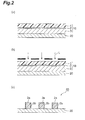
- a method for forming a conductive pattern according to the present embodiment includes a step ( Figure 2 (a) ) of laminating the photosensitive conductive film 10 so that the photosensitive resin layer 3 is tightly attached onto the substrate 20; an exposure step ( Figure 2(b) ) of irradiating a predetermined part of the photosensitive resin layer 3 on the substrate 20 with actinic light; and a development step of developing the exposed photosensitive resin layer 3 to form a conductive pattern. Going through the steps, a conductive film substrate 40 provided with a patterned conductive film (a conductive pattern) 2a on the substrate 20 can be obtained ( Figure 2 (c) ).
- the lamination step is conducted, in case a protection film exists, after removing the same, for example, by a method of laminating the photosensitive conductive film under heating by pressing tightly the photosensitive resin layer side onto the substrate. Concerning this operation, the lamination is preferably conducted under a reduced pressure from a viewpoint of an adhesion property and a following-up property.
- the photosensitive resin layer and/or the substrate is preferably heated to 70 to 130°C, and the pressing pressure is preferably about 0.1 to 1.0 MPa (about 1 to 10 kgf/cm 2 ), though there are no particular restrictions on the above conditions.
- the substrate is not required to be subjected to a preheating treatment in advance, but the substrate may be subjected to the preheating treatment to improve further the lamination property.
- Examples of an exposure method at the exposure step include a method (a mask exposure method), by which irradiation with actinic light is made through a negative or positive mask pattern, which is called as an artwork, in the form of an image.
- a light source for the actinic light a publicly known light source emitting effectively ultraviolet light, visible light, etc., such as an a carbon are lamp, a mercury vapor arc lamp, an ultrahigh pressure mercury lamp, a high pressure mercury lamp, and a xenon lamp, is used.
- an Ar ion laser, a semiconductor laser, etc., that emit effectively ultraviolet light, visible light, etc. can be also used.
- a photographic flood bulb, a sun lamp, etc. that emit effectively visible light can be also used.
- a method of irradiation with the actinic light in the form of an image by means of a direct writing method using a laser exposure method, etc. may be also adopted.
- the support film on the conducive layer is transparent to the actinic light
- the irradiation with the actinic light through the support film is possible
- the support film is light-blocking
- the photosensitive resin layer is irradiated with the actinic light after removal of the support film.
- the substrate is transparent to the actinic light
- the irradiation with the actinic light from the substrate side through the substrate is possible, but in view of the resolution it is preferable to irradiate the conductive layer and the photosensitive resin layer from the conductive layer side with the actinic light.
- the conductive layer 2a containing conductive fiber remains on the cured resin layer 3a having a predetermined pattern to form a conductive pattern.
- the wet development is conducted using a developing solution corresponding to a photosensitive resin, such as an alkaline aqueous solution, a water-based developing solution, and an organic solvent-based developing solution, according to a publicly known process, such as spraying, swinging immersion, brushing, and scraping.
- a photosensitive resin such as an alkaline aqueous solution, a water-based developing solution, and an organic solvent-based developing solution
- a solution such as an alkaline aqueous solution, which is safe and stable, as well as superior in usability, is utilized.
- a base for the alkaline aqueous solution to be utilized include an alkali hydroxide, such as a hydroxide of lithium, sodium or potassium; an alkali carbonate, such as a carbonate or a bicarbonate of lithium, sodium, potassium or ammonium; an alkali metal phosphate, such as potassium phosphate, and sodium phosphate; and an alkali metal pyrophosphate, such as sodium pyrophosphate, and potassium pyrophosphate.
- an alkaline aqueous solution used for development are preferable a 0.1 to 5% by mass aqueous solution of sodium carbonate, a 0.1 to 5% by mass aqueous solution of potassium carbonate, a 0.1 to 5% by mass aqueous solution of sodium hydroxide, a 0.1 to 5% by mass aqueous solution of sodium tetraborate, etc.
- the pH of an alkaline aqueous solution used for development is preferably adjusted to a range of 9 to 11, and the temperature thereof is regulated according to the developability of a photosensitive resin layer.
- a surfactant, a defoaming agent, and a small amount of an organic solvent for promoting development may be admixed.
- a water-based developing solution composed of water or an alkaline aqueous solution and one or more organic solvents
- examples of a base to be contained in the alkaline aqueous solution include, in addition to the afore described bases, borax and sodium metasilicate, tetramethylammonium hydroxide, ethanolamine, ethylenediamine, diethylenetriamine, 2-amino-2-hydroxymethyl-1,3-propanediol, 1,3-diaminopropanol-2, and morpholine.
- organic solvent examples include triacetone alcohol, acetone, ethyl acetate, an alkoxyethanol having an alkoxy group having 1 to 4 carbon atoms, ethyl alcohol, isopropyl alcohol, butyl alcohol, diethylene glycol monomethyl ether, diethylene glycol monoethyl ether, and diethylene glycol monobutyl ether. Either one thereof singly, or a combination of two or more thereof is used.
- the concentration of an organic solvent in a water-based developing solution is preferably adjusted to 2 to 90% by mass, and the temperature thereof can be regulated according to the developability.
- the pH of a water-based developing solution should be preferably selected as low as possible, as long as the development of a resist can be carried out sufficiently, and adjustment to pH 8 to 12 is preferable, more preferable to pH 9 to 10.
- a small amount of a surfactant, a defoaming agent, etc. can be admixed.
- Examples of an organic solvent-based developing solution include 1,1,1-trichloroethane, N-methylpyrrolidone, N,N-dimethylformamide, cyclohexanone, methyl isobutyl ketone, and ⁇ -butyrolactone. These organic solvents should preferably be used by adding water to a range of 1 to 20% by mass to avoid ignition.
- the aforedescribed developing solutions may be used according to need in combination of two or more thereof.
- Examples of a process for developing include a dipping process, a puddle process, a spraying process, brushing, and slapping. Among them the use of the high-pressure spraying process is preferable from a standpoint of improving the resolution.
- the conductive pattern may be additionally cured according to need after the development by heating to about 60 to 250°C or exposure at about 0.2 to 10 J/cm 2 .
- a transparent conductive pattern can be easily formed on a substrate made of glass, plastic or the like without forming an etching resist as for an inorganic film with ITO, etc.
- a conductive film substrate according to the present invention can be obtained by the method for forming a conductive film or the method for forming a conductive pattern, and from a standpoint that the same can be utilized effectively as a transparent electrode, the surface resistivity of the conductive film or the conductive pattern is preferably 2000 ⁇ /square or less, more preferably 1000 ⁇ /square or less, and especially preferably 500 ⁇ /square or less.
- the surface resistivity can be regulated, for example, by the concentration of a conductive fiber dispersion liquid, or the coating amount.
- the minimum light transmittance of a conductive film substrate according to the present invention in a wavelength range of 450 to 650 nm is preferably 80% or higher, and more preferably 85% or higher.
- a conductive fiber dispersion liquid 1 Into purified water were dispersed a high purity product of Hipco monolayer carbon nanotube (by Unidym, Inc.) to the concentration of 0.4% by mass, and dodecyl-pentaethylene glycol as a surfactant to 0.1% by mass, to obtain a conductive fiber dispersion liquid 1.
- Hipco monolayer carbon nanotube by Unidym, Inc.
- the above reaction solution was left standing to 30°C or less, then diluted 10-fold by acetone, and centrifuged by a centrifuge at 2000 rpm for 20 min to decant the supernatant liquid.
- Acetone was added to the sediment, and after stirring, the mixture was centrifuged under the similar conditions as above to decant the acetone. Thereafter, the similar centrifugation was repeated twice using distilled water to obtain silver fiber. According to observation of the obtained silver fiber under a light microscope, the fiber diameter was about 5 nm and the fiber length was about 5 ⁇ m.
- solution, a a solution of the mixture of 100 g of methacrylic acid, 250 g of methyl methacrylate, 100 g of ethyl acrylate and 50 g of styrene, a well as 0.8 g of azobisisobtityronitrile (hereinafter referred to as "solution, a") as monomers was prepared.
- solution, a 0.8 g of azobisisobtityronitrile
- the solution after the dropping was incubated at 80°C for 3 hours, and heated up to 90°C over 30 min.
- the solution was incubated at 90°C for 2 hours, and then cooled down to obtain a binder polymer solution,
- To the binder polymer solution was added acetone to adjust the solution so that a nonvolatile component (solid content) had 50% by mass, to obtain a binder polymer solution as the (a) component-
- the weight-average molecular weight of the obtained binder polymer was 80,000, which was designated as the acrylic polymer A.
- the conductive fiber dispersion liquid 1 obtained as above was coated uniformly at 25 g/m 2 onto a 50 ⁇ m-thick polyethylene terephthalate film (PET films, Trade name "G2-50", by Teijin Limited) as a support film, dried in a hot air convection drier at 100°C for 3 min, and pressed at a linear pressure of 10 kg/cm at room temperature to form a conductive layer on the support film.
- the film thickness of the conductive layer after drying was about 0.02 ⁇ m.
- the solution of the photosensitive resin composition was coated uniformly onto the 50 ⁇ m-thick polyethylene terephtalate film, on which the conductive layer had been formed, and dried in a hot air convection drier at 100°C for 10 min to form a photosensitive resin layer. Thereafter the photosensitive resin layer was covered by a polyethylene protection film (Trade name "NF-13", by Tamapoly Co., Ltd.) to obtain a photosensitive conductive film.
- the film thickness of the photosensitive resin layer after drying was 5 ⁇ m.
- the conductive fiber dispersion liquid 2 obtained as above was coated uniformly at 25 g/m 2 onto a 50 ⁇ m-thick polyethylene terephthalate film (PET film, Trade name "G2-50", by Teijin Limited) as a support film, dried in a hot air convection drier at 100°C for 10 min, and pressed at a linear pressure of 10 kg/cm at room temperature to form a conductive layer on the support film.
- PET film polyethylene terephthalate film, Trade name "G2-50", by Teijin Limited
- the film thickness of the conductive layer after drying was about 0.01 ⁇ m.
- the solution of the photosensitive resin composition was coated uniformly onto the 50 ⁇ m-thick polyethylene terephthalate film, on which the conductive layer had been formed, and dried in a hot air convection drier at 100°C for 10 min to form a photosensitive resin layer. Thereafter the photosensitive resin layer was covered by a polyethylene protection film (Trade name "NF-13", by Tamapoly Co., Ltd.) to obtain a photosensitive conductive film, The film thickness or the photosensitive resin layer after drying was 5 ⁇ m.
- Polycarbonate substrates with the thickness of 1 mm were heated to 80°C, and on the surfaces thereof the photosensitive conductive films obtained in Examples 1 and 2 were laminated by delaminating the protection film with the photosensitive resin layer facing the substrate under the conditions of 120°C and 0,4 MPa. After the lamination, the substrates were cooled, and when the substrate temperature reached 23°C, the conductive layers and the photosensitive resin layers were irradiated with light from the support film side using an exposure machine with a high pressure mercury lamp (Trade name "HMW-201B", by Ore Manufacturing Co., Ltd.) at the exposure dose of 1000 mJ/cm 2 .
- a high pressure mercury lamp Trade name "HMW-201B", by Ore Manufacturing Co., Ltd.
- the PET films as the support film were delaminated to form conductive films containing carbon nanotube or silver fiber on the polycarbonate substrates.
- the surface resistivities of the respective conductive films were 2000 ⁇ /square and 500 ⁇ /square, and the minimum light transmittances (including the substrates) in a wavelength range of 450 to 650 nm were 80%, and 85%.
- the conductive films were formed on the glass substrate using the photosensitive conductive films obtained in Examples 1 and 2.
- the surface resistivities of the respective conductive films were 2000 ⁇ /square and 500 ⁇ /square, and the minimum light transmittances (including the substrates) in a wavelength range of 450 to 650 nm were 82%, and 87%. Meanwhile, the surface resistivity and the transmittance were measured according to the following methods.
- the surface resistivity was measured using a low resistivity meter (Loresta GP, by Mitsubishi Chemical Corporation) by a 4-point probe technique according to JIS K 7194.
- the light transmittance at 450 nm, 550 nm and 650 nm, and the minimum light transmittances in a wavelength range of 450 to 650 nm were measured using a spectrophotometer (Trade name "U-3310", by Hitachi High-Technologies Corporation).
- a conductive layer was formed identically with Example 1, and a photosensitive conductive film was produced identically with Example 1, except that a photosensitive resin layer was so formed to make the total film thickness of the conductive layer and the photosensitive resin layer to 10 ⁇ m.
- a conductive layer was formed identically with Example 2, and a photosensitive conductive film was produced identically with Example 2, except that a photosensitive resin layer was so formed to make the total film thickness of the conductive layer and the photosensitive resin layer to 10 ⁇ m.
- the photosensitive conductive film obtained as above was laminated on the 1 mm-thick polycarbonate substrate heated to 80°C by delaminating the protection film with the photosensitive resin layer facing the substrate under the conditions of 120°C and 0.4 MPa. After the lamination, the substrate was cooled, and when the substrate temperature reached 23°C, the conductive layer and the photosensitive resin layer were irradiated with light from the support film side using an exposure machine with a high pressure mercury lamp (Trade name "HMW-201B", by Ore Manufacturing Co., Ltd.) at the exposure dose of 1000 mJ/cm 2 . After the exposure the laminate was left standing at room temperature (25°C) for 15 min, then the PET film, namely the support film, was delaminated to form a conductive film containing carbon nanotube or silver fiber on the polycarbonate substrate,
- the light transmittance at 450 nm, 550 nm and 650 nm, and the minimum light transmittance in a wavelength range of 450 to 650 nm of the conductive layer containing conductive fiber and the photosensitive resin layer were measured using a spectrophotometer (Trade name "U-3310", by Hitachi High-Technologies Corporation). The evaluation results are shown in Table 2.
- Example 3 Conductive fiber Carboy nanotube Silver fiber Thickness of conductive layer ( ⁇ m) 0.02 0.01 Total film thickness of conductive layer and photosensitive resin layer ( ⁇ m) 10 10 10 Minimum light transmittance in a wavelength range of 450 to 650 run (%) 80.4 89.1 Light transmittance (%) Wavelength 450nm 80.4 89.1 Wavelength 550nm 84.5 93.7 Wavelength 650nm 85.8 94.8
- Polycarbonate substrates with the thickness of 1 mm were heated to 80°C, and on the surfaces thereof the photosensitive conductive films obtained in Examples 1 and 2 were laminated by delaminating the protection film with the photosensitive resin layer facing the substrate under the conditions of 120°C and 0.4 MPa.
- the substrate was cooled, and when the substrate temperature reached 23°C, a photomask having an interconnection pattern of the line width / space width of 100 / 100 ⁇ m and the length of 100 mm was tightly attached onto the surface of the PET film, namely the support film, Then the conductive layer and the photosensitive resin layer were irradiated with light using an exposure machine with a high pressure mercury lamp (Trade name "HMW-201B", by Ore Manufacturing Co., Ltd.) at the exposure dose of 200 mJ/cm 2 .
- a high pressure mercury lamp Trade name "HMW-201B", by Ore Manufacturing Co., Ltd.
- the laminate was left standing at room temperature (25°C) for 15 min, then the PET film, namely the support film, was delaminated and developed by spraying a 1% by mass aqueous solution of sodium carbonate at 30°C for 30 sec. After the development, a conductive pattern having a line width / space width of about 100/100 ⁇ m of the conductive film containing carbon nanotube or silver fiber was formed on the polycarbonate substrate. It was confirmed that the respective conductive patterns were formed satisfactorily.
- a photosensitive conductive film enabling with ease formation, on a substrates, of a sufficiently high resolution conductive pattern having sufficient adherence with the substrate and sufficiently low surface resistivity; as well as a method for forming a conductive film using the photosensitive conductive film; a method for forming a conductive pattern; and a conductive film substrate can be provided.
Abstract
Description
- The present invention relates to a photosensitive conductive film, a method for forming a conductive film, a method for forming a conductive pattern, and a conductive film substrate; and particularly to a method for forming a conductive pattern to be used as an electrode interconnection of an apparatus, such as a flat panel display with a liquid crystal display element, etc., a touch screen and a solar cell, and a conductive film substrate.
- For a larger electronic device, such as a personal computer and a television, a car navigation device, a cell phone, a smaller electronic device such as an electronic dictionary, and a display device or an OA/FA device, use of a liquid crystal display element or a touch screen has become popular. In such a liquid crystal display element and a touch screen, as well as a device such as a solar cell, a transparent conductive film is used for a part of an interconnection, a pixel electrode or a terminal, which requires transparency.
- As a material for a transparent conductive film, ITO (Indium-Tin-Oxide), indium oxide and tin oxide, which exhibit high transmittance for visible light, have been heretofore used. For an electrode of a substrate for a liquid crystal display element, a patterned transparent conductive film consisting of the above material has become mainstream.
- As a patterning method of a transparent conductive film is common a method by which after the formation of a transparent conductive film, a resist pattern is formed by a photolithography, and a predetermined part of the conductive film is removed by wet etching to form a conductive pattern. In the case of an ITO and indium oxide film, a mixture solution consisting of 2 liquids of hydrochloric acid and ferric chloride is commonly used as an etching solution.
- An ITO film or a tin oxide film is formed generally by a sputtering method. By this method, however, the properties of the transparent conductive film change sensitively depending on the difference of the sputtering method, a power or gas pressure of a sputter, a substrate temperature, or a type of the atmospheric gas. The difference of the film quality of a transparent conductive film caused by a fluctuation of the sputtering conditions can cause fluctuation in the etching speed, when the transparent conductive film is subjected to wet etching, which may lead to a lower product yield by reason of poor patterning. Further, the above method for forming a conductive pattern must go through a step of sputtering, a step of forming resist, and a step of etching, and therefore the process is long, which constitutes a heavy burden costwise.
- To solve the above problem, an attempt has been made recently to use an alternative material to ITO, indium oxide, tin oxide, etc. to form a transparent conductive pattern. For example, in the following
Patent Literature 1 is disclosed a method for forming a conductive pattern, by which a conductive layer containing conductive fiber such as silver fiber is formed on a substrate, then a photosensitive resin layer is formed on the conductive later, the former is exposed to light from above through a pattern mask, and developed. - Patent Literature 1:
U.S. Patent Application Publication No. 2007/0074316 - However, according to the study of the present inventor, it has been known that, by the method described in the
Patent Literature 1, the surface resistivity of a conductive pattern can hardly be made to low resistivity, while assuring the adherence between a substrate and a conductive pattern. Further, in case the conductive pattern is used as an interconnection, a pixel electrode or a terminal, a step of removing a photosensitive resin layer is required, and there arises a problem that a process for forming a conductive pattern becomes complex. - The present invention has been made in view of the problems involved in the conventional art, with objects to provide a photosensitive conductive film enabling with ease formation, on a substrate, of a sufficiently high resolution conductive pattern having sufficient adherence with the substrate and sufficiently low surface resistivity; as well as a method for forming a conductive film using the photosensitive conductive film; a method for forming a conductive pattern; and a conductive film substrate.
- To solve the problem, the present invention provides a photosensitive conductive film comprising a support film, a conductive layer containing conductive fiber formed on the support film, and a photosensitive resin layer formed on the conductive layer.
- With a photosensitive conductive film according to the present invention by reason of having the above constitution, it becomes possible to form a conductive pattern having sufficient adherence with a substrate and sufficiently low surface resistivity at a sufficient resolution by a simple process, in which a photosensitive conductive film is laminated so that a photosensitive resin layer is tightly attached onto a substrate, and the same is then exposed and. developed.
- With respect to the photosensitive conductive film according to the present invention, the minimum light transmittance in a wavelength range of 450 to 650 nm of a laminate of the conductive layer and the photosensitive resin layer is preferably 80% or higher, provided that the total film thickness of the two layers is set at 1 to 10 µm. In case the conductive layer and the photosensitive resin layer satisfy the above conditions, higher brightness of a display panel, etc, becomes easy to achieve.
- With respect to the photosensitive conductive film according to the present invention, the conductive fiber is preferably silver fiber from a viewpoint of easiness in adjusting the conductivity of the conductive film to be formed.
- It is preferable that the photosensitive resin layer contains a binder polymer, a photopolymerizable compound having an ethylenic unsaturated bond, and a photopolymerization initiator, from a standpoint of further improving the adherence between the substrate and the conductive pattern, and the patterning property of the conductive film.
- The present invention provides further a method for forming a conductive film comprising a lamination step of laminating the photosensitive conductive film according to the present invention so that the photosensitive resin layer is tightly attached onto a substrate; and an exposure step of irradiating the photosensitive resin layer on the substrate with actinic light.
- According to the method for forming a conductive film according to the present invention, a conductive film having sufficient adherence with a substrate and sufficiently low surface resistivity can be easily formed on a substrate by using the photosensitive conductive film according to the present invention and conducting the above steps.
- The present invention provides further a method for forming a conductive pattern comprising a step of laminating the photosensitive conductive film according to the present invention so that the photosensitive resin layer is tightly attached onto a substrate; an exposure step of irradiating a predetermined part of the photosensitive resin layer on the substrate with actinic light; and a development step of developing the exposed photosensitive resin layer to form a conductive pattern.
- According to the method for forming a conductive pattern, a conductive pattern having sufficient adherence with a substrate and sufficiently low surface resistivity can be formed on a substrate simply and at a sufficient resolution by using the photosensitive conductive film according to the present invention and conducting the above steps.
- The present invention provides further a conductive film substrate comprising a substrate and a conductive film formed on the substrate by the method for forming a conductive film according to the present invention.
- The present invention provides further a conductive film substrate comprising a substrate and a conductive pattern formed on the substrate by the method for forming a conductive pattern according to the present invention.
- With respect to the conductive film substrate according to the present invention, the surface resistivity of the conductive film or the conductive pattern is preferably 2000 Ω/square or less.
- According to the present invention, a photosensitive conductive film enabling with ease formation, on a substrate, of a sufficiently high resolution conductive pattern having sufficient adherence with the substrate and sufficiently low surface resistivity; as well as a method for forming a conductive film using the photosensitive conductive film; a method for forming a conductive pattern; and a conductive film substrate, can be provided.
-
-
Figure 1 is a schematic cross-section showing an embodiment of a photosensitive conductive film according to the present invention, and -
Figure 2 is a schematic cross-section illustrating an embodiment of a method for forming a conductive pattern according to the present invention. - Favorable embodiments of the present invention will be described below in detail. Meanwhile, "(meth)acrylate" herein means "acrylate" and the corresponding "methacrylate". Similarly, "(meth)acryl" means "acryl" and the corresponding "methacryl", and "(meth)acryloyl" means "acryloyl" and the corresponding "methacryloyl".
-
Figure 1 is a schematic cross-section showing a favorable embodiment of a photosensitive conductive film according to the present invention. A photosensitiveconductive film 10 inFigure 1 includes asupport film 1, aconductive layer 2 containing conductive fiber provided on thesupport film 1, and aphotosensitive resin layer 3 provided on theconductive layer 2. - The
support film 1, theconductive layer 2 containing conductive fiber, and thephotosensitive resin layer 3, constituting the photosensitiveconductive film 10 will each be described in detail below. - Examples of the
support film 1 includes a polymer film having heat resistance and solvent resistance, such as a polyethylene terephthalate film, a polyethylene film, a polypropylene film, and a polycarbonate film. Among them, from a standpoint of transparency and heat resistance, a polyethylene terephthalate film is preferable. Meanwhile, the polymer films must be strippable later from a photosensitive resin layer, they must not be subjected to a surface treatment, or use a material, by which stripping becomes impossible. - The thickness of the
support film 1 is preferably 5 to 300 µm, more preferably 10 to 200 µm, and especially preferably 15 to 100 µm. In case the thickness of the support film is less than 5 µm, the mechanical strength is lowered, and the support film tends to tear easily at a step of coating a dispersion liquid of conductive fiber to form theconductive layer 2 or a photosensitive resin composition to form thephotosensitive resin layer 3, or a step of delaminating the support film before developing the exposedphotosensitive resin layer 3. While, in case the thickness of the support film exceeds 300 µm, the resolution of a pattern tends to decrease, when the photosensitive resin layer is irradiated with actinic light through the support film, and further the cost tends to increase. - The haze value of the
support film 1 is preferably 0.01 to 5.0% from a standpoint of good sensitivity and resolution, more preferably 0.01 to 3.0%, especially preferably 0.01 to 2.0%, and extremely preferably 0.01 to 1.0%. Meanwhile, the haze value may be measured according to JIS K 7105, and can be measured by a commercially available haze meter, such as NDH-1001DP (Trade name, by Nippon Denshoku Industries, Co., Ltd.) - Examples of conductive fiber to be contained in the
conductive layer 2 include metal fiber, such as gold, silver, and platinum, and carbon fiber such as carbon nanotube. Either one thereof singly, or a combination of two or more thereof may be used. From a standpoint of conductivity, use of gold fiber or silver fiber is preferable. Either one of gold fiber and silver fiber singly, or a combination of two or more thereof may be used. Further, from a standpoint of easy regulation of the conductivity of a conductive film to be formed, silver fiber is more preferable. - The metal fiber can be prepared, for example, by a method of reducing a metal ion by a reducing agent such as NaBH4, or a polyol method.
- As carbon nanotube, a commercially available product, such as HiPco monolayer carbon nanotube by Unidym, Inc., can be used.
- The fiber diameter of conductive fiber is preferably 1 nm to 50 nm, more preferably 2 nm to 20 nm, and especially preferably 3 nm to 10 nm. The fiber length of the conductive fiber is preferably 1 µm to 100 µm, more preferably 2 µm to 50 µm, and especially preferably 3 µm to 10 µm. The fiber diameter and fiber length can be measured by a scanning electron microscope.
- The thickness of the
conductive layer 2, which may vary depending on the use or the required conductivity of a conductive film or a conductive pattern to be formed using photosensitive conductive film according to the present invention, is preferably 1 µm or less, more preferably 1 nm to 0.5 µm, and especially preferably 5 nm to 0.1 µm. In case the thickness of theconductive layer 2 is 1 µm or less, the light transmittance in a wavelength range of 450 to 650 nm is high, and the pattern formability is also excellent, which is favorable especially for producing a transparent electrode. - The
conductive layer 2 has preferably a network structure formed by contacting conductive fibers each other. Theconductive layer 2 with such a network structure may be constructed on a surface of thephotosensitive resin layer 3 facing the support film, but it may also be constructed in a form to be embedded in a surface layer of thephotosensitive resin layer 3 facing the support film, as long as a surface to become exposed by delaminating the support film is conductive in the direction of the surface plane. The thickness of theconductive layer 2 with a network structure means a value measured by a scanning electron micrograph. - The
conductive layer 2 containing conductive fiber can be formed, for example, by coating a conductive fiber dispersion liquid containing the aforedescribed conductive fiber, water and/or an organic solvent, and according to need a dispersion stabilizer such as a surfactant, onto thesupport film 1, followed by drying. After drying, theconductive layer 2 formed on thesupport film 1 may be laminated, according to need. Coating may be carried out by a publicly known method, such as a roll coating method, a comma coating method, a gravure coating method, an air knife coating method, a die coating method, a bar coating method, and a spray coating method. Further, drying may be carried out at 30 to 150°C for about 1 to 30 min in a hot air convection drier, etc. In theconductive layer 2, the conductive fiber may coexist with a surfactant and a dispersion stabilizer. - Examples of the
photosensitive resin layer 3 include those prepared from a photosensitive resin composition containing (a) a binder polymer, (b) a photopolymerizable compound having an ethylenic unsaturated bond, and (c) a photopolymerization initiator. - Examples of (a) a binder polymer include an acrylic resin, a styrene resin, an epoxy resin, an amide resin, an amide-epoxy resin, an alkyd resin, a phenol resin, an ester resin, a urethane resin, an epoxy acrylate resin obtained by a reaction between an epoxy resin and (meth)acrylic acid, and an acid-modified epoxy acrylate resin obtained by a reaction between an epoxy acrylate resin and an acid anhydride. Either one of the resins singly, or a combination of two or more thereof may be used. From a standpoint of a good alkali development property and film formation property, it is preferable to use an acrylic resin, and more preferable that the acrylic resin has as constituent units monomer units derived from (meth)acrylic acid and a (meth)acrylic acid alkyl ester. The term "acrylic resin" means a polymer having mainly a monomer unit derived from a polymerizable monomer having a (meth)acrylic group. Further, herein "(meth)acrylic acid" means "acrylic acid" and the corresponding "methacrylic acid", and a "(meth)acrylic acid alkyl ester" means an "acrylic acid alkyl ester" and the corresponding "methacrylic acid alkyl ester".
- As the acrylic resin, one produced by a radical polymerization of a polymerizable monomer having a (meth)acrylic group can be used. Either one of the acrylic resin singly, or a combination of two or more thereof may be used.
- Examples of the polymerizable monomer having a (meth)acrylic group include acrylamide such as diacetone acrylamide, a (meth)acrylic acid alkyl ester, (meth) acrylic acid tetrahydrofurfuryl ester, (meth)acrylic acid dimethylaminoethyl ester, (meth)acrylic acid diethylaminoethyl ester, (meth)acrylic acid glycidyl ester, 2,2,2-trifluoroethyl (meth)acrylate, 2,2,3,3-tatrafluoropropyl (meth)acrylate, (meth)acrylic acid, α-bromo(meth)acrylic acid, α-chloro(meth)acrylic acid, β-furyl (meth)acrylic acid, and β-styryl (meth)acrylic acid.
- The acrylic resin may be copolymerized with one or two or more of polymerizable monomers, such as, in addition to the above polymerizable monomer having a (meth)actylic group, styrene, a polymerizable derivative of styrene substituted at the α-position or in an aromatic ring (e.g., vinyl toluene and α-methylstyrene), acrylonitrile, esters of vinyl alcohol (e.g., vinyl-n-butyl ether), maleic acid, maleic anhydride, a maleic acid mono ester (e.g., monomethyl maleate, monoethyl maleate, monoisopropyl maleate), fumaric acid, cinnamic acid, α-cyanocinnamic acid, itaconic acid, and crotonic acid.
- Examples of the (meth)acrylic acid alkyl ester include the compounds expressed by the following general formula (1) and compounds in which an alkyl group of the former compounds is substituted by a hydroxy group, an epoxy group, a halogen group, etc.
CH2=C(R1)-COOR2 (1)
- In the formula R1 represents a hydrogen atom or a methyl group, R2 represents an alkyl group having 1 to 12 carbon atoms. Examples of the alkyl group having 1 to 12 carbon atoms include a methyl group, an ethyl group, a propyl group, a butyl group, a pentyl group, a hexyl group, a heptyl group, an octyl group, a nonyl group, a decyl group, an undecyl group, a dodecyl group and a structural isomer thereof.
- Examples of the compounds expressed by the above general formula (1) include methyl (meth)acrylate, ethyl (meth)acrylate, propyl (meth)acrylate, butyl (meth)acrylate, pentyl (meth)acrylate, hexyl (meth)acrylate, heptyl (meth)acrylate, octyl (meth)acrylate, 2-ethylhexyl (meth)acrylate, nonyl (meth)acrylate, decyl (meth)acrylate, undecyl (meth)acrylate, and dodecyl (meth)acrylate. Either one thereof singly, or a combination of two or more thereof may be used.
- Further, (a) a binder polymer should preferably have a carboxyl group from a standpoint of better alkali developability. Examples of a polymerizable monomer includes (meth)acrylic acid as described above.
- The content of a carboxyl group contained in a binder polymer in terms of the ratio of a polymerizable monomer having a carboxyl group to the total polymerizable monomers used, is preferably 12 to 50% by mass from a standpoint of well balanced alkali developability and alkali resistance, more preferably 12 to 40% by mass, especially preferably 15 to 30% by mass, and extremely preferably 15 to 25% by mass. In case the content of the polymerizable monomer having a carboxyl group is less than 12% by mass the alkali developability is apt to be poor, and in case it exceeds 50% by mass the alkali resistance is apt to be poor.
- The weight-average molecular weight of the binder polymer is preferably 5,000 to 300,000 from a standpoint of well balanced mechanical strength and alkali developability, more preferably 20,000 to 150,000, and especially preferably 30,000 to 100,000. In case the weight-average molecular weight is less than 5,000, the resistance to a developing solution tends to decrease, and in case it exceeds 300,000, the developing time tends to extend. The weight-average molecular weight in the present invention is a value measured by a gel permeation chromatography method (GPC) and converted according to a calibration curve prepared by using a standard polystyrene.
- Either one of the binder polymers singly, or a combination of two or more thereof may be used. In case a combination of two or more thereof is used, examples of the binder polymers include two or more binder polymers containing different comonomer constituents, two or more binder polymers having different weight-average molecular weights, and two or more binder polymers having different degrees of dispersion.
- Next, (b) a photopolymerizable compound having an ethylenic unsaturated bond will be described.
- As a photopolymerizable compound having an ethylenic unsaturated bond, a photopolymerizable compound having an ethylenic unsaturated bond is preferable. Examples of a photopolymerizable compound having an ethylenic unsaturated bond include a compound obtained by reacting polyhydric alcohol with α,β-unsaturated carboxylic acid, a bisphenol A type (meth)acrylate compound, such as a 2,2-bis(4-((meth)acryloxypolyethoxy)phenyl)propane, a 2,2-bits(4-((meth)acryloxypolypropoxy)phenyl)propane, and a 2,2-bis(4-((meth)acryloxypolyethoxypolypropoxy)phenyl)propane, a compound obtained by reacting a compound containing a glycidyl group with α,β-unsaturated carboxylic acid, a urethane monomer such as a (meth)acrylate compound having a urethane bond, γ-chloro-β-hydroxypropy-β'-(meth)acryloyloxyethyl-o-phthalate, β-hydroxyethyl-β'-(meth)acryloyloxyethyl-o-phthalate, β-hydroxypropyl-β'-(meth)acryloyloxyethyl-o-phthalate, and a (meth)acrylic acid alkyl ester. They may be used singly, or in combination of two or more thereof.
- Example of a 2,2-bis(4-((meth)acryloxypolyethoxy)phenyl)propane include 2,2-bis(4-((meth)acryloxydiethoxy)phenyl)propane, 2,2-bins(4-((meth)acryloxytriethoxy)phenyl)propane, 2,2-bis(4-((meth)acryloxytetraethoxy)phenyl)propane, 2,2-bis(4-((meth)acryloxypentaethoxy)phenyl)propane, 2,2-bis(4-((meth)acryloxyhexaethoxy)phenyl)propane, 2,2-bis(4-((meth)acryloxyheptaothoxy)phenyl)propane, 2,2-bis(4-((meth)acryloxyoctaethoxy)phenyl)propane, 2,2-bis(4-((meth)acryloxynonaethoxy)phenyl)propane, 2,2-bis(4-((meth)acryloxydecaethoxy)phenyl)propane, 2,2-bis(4-((meth)acryloxyundecaethoxy)phenyl)propane, 2,2-bis(4-((meth)acryloxydodecaethoxy)phenyl)propane, 2,2-bis(4-((meth)acryloxytridecaethoxy)phenyl)propane, 2,2-bis(4-((meth)acryloxytetradecaethoxy)phenyl)propane, 2,2-bis(4-((meth)acryloxypentadecaethoxy)phenyl)propane, and 2,2-bis(4-((meth)acryloxyhexadecaethoxy)phenyl)propane. Among them 2,2-bis(4-(methacryloxypentaethoxy)phenyl)propane is commercially available as "BPE-500" (Trade name, from Shin-Nakamura Chemical Co., Ltd.), and 2,2-bis(4-(methacryloxypentadecaethoxy)phenyl)propane is commercially available as "BPE-1300" (Trade name, from Shin-Nakamura Chemical Co., Ltd.). They may be used singly, or in combination of two or more thereof.
- Examples of the compound obtained by reacting polyhydric alcohol with α,β-unsaturated carboxylic acid include a polyethylene glycol di(meth)acrylate with 2 to 14 ethylene groups, a polypropylene glycol di(meth)acrylate with 2 to 14 propylene groups, a polyethylene polypropylene glycol di(meth)acrylate with 2 to 14 ethylene groups and 2 to 14 propylene groups, trimethylol propane di(meth)acrylate, trimethylol propane tri(meth)acrylate, trimethylol propane ethoxytri(meth)acrylate, trimethylol propane diethoxytri(meth)acrylate, trimethylol propane triethoxytri(meth)acrylate, trimethylol propane tetraethoxytri(meth)acrylate, trimethylol propane pentaethoxytri(meth)acrylate, tetramethylol methane tri(meth)acrylate, tetramethylol methane tetra(meth)acrylate, a polypropyleneglycol di(meth)acrylate with 2 to 14 propylene groups, dipentaerythritol penta(meth)acrylate, and dipentacrythritol hexa(meth)acrylate.
- Examples of the urethane monomer include an addition product of (meth)acrylic monomer having a hydroxyl group at the β-position with a diisocyanate compound, such as isophorone diisocyanate, 2,6-toluene diisocyanate, 2,4-toluene diisocyanate, and 1,6-hexamethylene diisocyanate, tris[(meth)acryloxytetraethylene glycol isocyanate]hexamethylene isocyanurate, an EO-modified urethane di(meth)acrylate, and an EO, PO-modified urethane di(meth)acrylate. Meanwhile, "EO" stands for ethylene oxide, and an EO-modified compound has a block structure of ethylene oxide groups. "PO" stands for propylene oxide, and a PO-modified compound has a block structure of propylene oxide groups. Examples of an EO-modified urethane di(meth)acrylate include "UA-11" (Trade name, by Shin-Nakamura Chemical Co., Ltd.), and examples of an EO, PO-modified urethane di(meth)acrylate include "UA-13" (Trade name, by Shin-Nakamura Chemical Co., Ltd.).
- The content of a photopolymerizable compound is preferably 30 to 80 parts by mass based on total 100 parts by mass of a binder polymer and a photopolymerizable compound, and more preferably 40 to 70 parts by mass. In case the content is less than 30 parts by mass, light curing becomes insufficient, and the coating property of a transferred conductive film (a conductive layer and a photosensitive resin layer) tends to become insufficient, and in case it exceeds 80 parts by mass, the storage of a wound-up film tends to become difficult.
- Next, (c) a photopolymerization initiator will be described.
- Examples of a photopolymerization initiator include an aromatic ketone, such as benzophenone, N,N'-tetramethyl-4,4'-diaminobenzophenone (Michler ketone), N,N'-tetraethyl-4,4'-diaminobenzophenone, 4-methoxy-4'-dimethylaminobenzophenone, 2-benzyl-2-dimethylamino-1-(4-morpholinophenyl)-butanone-1, and 2-methyl-1-[4-(methylthio)phenyl]-2-morpholino-propanone-1, a quinone, such as 2-ethylanthraquinone, phenanthrenequinone, 2-tert-butylanthraquinone, octamethylanthraquinone, 1,2-benzanthraquinone, 2,3-benzanthraquinone, 2-phonylanthraquinone, 2,3-diphenylanthraquinone, 1-chloroanthraquinone, 2-methylanthraquinone, 1,4-naphthoquinone, 9,10-phenanthraquinone, 2-methyl-1,4-naphthoquinone, and 2,3-dimethylanthraquinone, a benzoin ether compound, such as benzoin methyl ether, benzoin ethyl ether, and benzoin phenyl ether, a benzoin compound, such as benzoin, methylbenzoin, and ethylbenzoin, an oxime ester compound, such as 1,2-octanedione-1-[4-(phenylthio)phenyl]-2-(O-benzoyloxime), and 1-[9-ethyl-6-(2-methylbenzoyl)-9H-carbazol-3-yl]ethanone 1-(O-acetyloxime), a benzyl derivative, such as benzyldimethylketal, a 2,4,5-triarylimidazole dimer, such as 2-(o-chlorophenyl)-4,5-diphenylimidazole dimer, 2-(o-chlorophenyl)-4,5-di(methoxyphenyl)imidazole dimer, 2-(o-fluorophenyl)-4,5-diphenylimidazole dimer, 2-(o-methoxyphenyl)-4,5-diphenylimidazole dimer, and 2-(p-methoxyphenyl)-4,5-diphenylimidazole dimer, an acridine derivative, such as 9-phenylacridine, and 1,7-bis(9,9'-acridmyl)heptane, N-phenylglycine, an N-phenylglycine derivative, a coumarin type compound, and an oxazole type compound, The substituents of an aryl group of the two of 2,4,5-triarylimidazole may be identical to give a symmetric compound, or different to give an asymmetric compound. Further, a thioxanthone type compound and a tert-amine compound may be combined as a combination of diethylthioxanthone and dimethylaminobenzoic acid, Among them, from a standpoint of transparency, an aromatic ketone compound, such as 2-benzyl-2-dimethylamino-1-(4-morphoinophenyl)-butanone-1, and an oxime ester compound, such as 1,2-octanedione-1-[4-(phenylthio)phenyl]-2-(O-benzoyloxime), are more preferable. They may be used singly, or in combination of two or more thereof.
- The content of a photopolymerization initiator is preferably 0.1 to 20 parts by mass based on total 100 parts by mass of a binder polymer and a photopolymerizable compound, more preferably 1 to 10 parts by mass, and especially preferably 1 to 5 parts by mass. In case the content is less than 0.1 parts by mass, the photosensitivity tends to become insufficient, and in case it exceeds 20 parts by mass, the absorption at the surface of a photosensitive resin layer on an occasion of exposure increases and the internal light curing tends to become insufficient.
- According to need, to the
photosensitive resin layer 3, an additive, such as a plasticizer (e.g., p-toluenesulfonamide), a filler, a defoaming agent, a flame retardant, a stabilizer, a tackifier, a leveling agent, a stripping agent, an antioxidant, a fragrance, an imaging agent, and a thermal cross-linking agent may be added singly, or in combination of two or more thereof. The addition amount of each additive is preferably 0.01 to 20 parts by mass based on total 100 parts by mass of a binder polymer and a photopolymerizable compound. - The
photosensitive resin layer 3 can be formed, on thesupport film 1 with theconductive layer 2 formed thereon, by coating a photosensitive resin composition solution, whose solid content is about 10 to 60% by mass dissolved in a solvent of methanol, ethanol, acetone, methyl ethyl ketone, methylcellosolve, ethylcellosolve, toluene, N,N-dimethylformamide, propylene glycol monomethyl ether, or a mixture solvent thereof according to need, and followed by drying. In this connection, the content of a residual organic solvent in the photosensitive resin layer after drying is preferably 2% by mass or less, so as to prevent diffusion of the organic solvent at a later process step. - The coating can be conducted according to a publicly known method, such as a roll coating method, a comma coating method, a gravure coating method, an air knife coating method, a die coating method, a bar coating method, and a spray coating method. The drying after the coating to remove an organic solvent, etc. may be conducted at 70 to 150°C for about 5 to 30 min by a hot air convection drier, etc.
- The thickness of the
photosensitive resin layer 3 may vary according to its application, and is preferably 1 to 200 µm as the thickness after drying, more preferably 1 to 15 µm, and especially preferably 1 to 10 µm. In case the thickness is less than 1 µm, the coating tends to become difficult, and in case it exceeds 200 µm, the sensitivity becomes insufficient due to decrease in light transmission and the light curing capability of the photosensitive resin layer to be transferred tends to decrease. - In a photosensitive conductive film according to the present embodiment, the minimum light transmittance in a wavelength range of 450 to 650 nm of a laminate of the
conductive layer 2 and thephotosensitive resin layer 3, when the total film thickness of the two layers is set at 1 to 10 µm, is preferably 80% or higher, and more preferably 85% or higher. In case the conductive layer and the photosensitive resin layer satisfy such conditions, higher brightness in a display panel, etc. becomes easy to achieve. - In a photosensitive conductive film according to the present invention, contacting the surface of the
photosensitive resin layer 3 opposite to the surface facing thesupport film 1, a protection film can be laminated, - As a protection film, for example, a polymer film with heat resistance and solvent resistance, such as a polyethylene terephthalate film, a polypropylene film, and a polyethylene film, can be used. Further, as a protection film, a polymer film similar to the afore described support film may be used.
- The bond strength of the protection film with the photosensitive resin layer is preferably less than the bond strengths of the
conductive layer 2 and thephotosensitive resin layer 3 with thesupport film 1, so as to facilitate delamination of the protection film from the photosensitive resin layer. - Further, as for the protection film, the number of fish eyes with the diameter of 80 µm or larger in the protection film is preferably 5/m2 or less. While, "fish eye" is a foreign substance in a material, an unmelted product, an oxidation degradation product, etc. included in a film, when the film is produced by hot melting, kneading and extruding a material, by a biaxial stretching or casting method, etc,
- The thickness of the protection film is preferably 1 to 100 µm, more preferably 5 to 50 µm, further preferably 5 to 30 µm, and especially preferably 15 to 30 µm. In case the thickness of the protection film is less than 1 µm, the protection film tends to tear easily in laminating, and in case it exceeds 100 µm, the cost tends to increase.
- The photosensitive conductive film may have an additional layer, such as an adhesive layer, and a gas barrier layer, on the support film.
- The photosensitive conductive film may be stored, for example, as it is in a flat sheet form, or in the form of a roll obtained by winding it around an, e.g., cylindrical core. In the latter case, the film is preferably so wound that the support film comes to the outermost side.
- In case the photosensitive conductive film does not have a protection film, such photosensitive conductive film can be stored as it is in a flat sheet form.
- There is no particular restriction on a core, as long as it has been used heretofore. Examples thereof include a plastic, such as a polyethylene resin, a polypropylene resin, a polystyrene resin, a polyvinylchloride resin, and an ABS resin (acrylonitrile-butadienestyrene copolymer). Further, at an end-face of the photosensitive conductive film wound in the form of a roll, an end separator is preferably provided from a standpoint of protecting the end-face, and further from a standpoint of the edge fusion resistance a moisture-proof end separator should be provided preferably. Further, in case a photosensitive conductive film is packaged, packaging in a low moisture permeability black sheet is preferable.
- A method for forming a conductive film according to the present invention includes a lamination step of laminating the photosensitive conductive film according to the present invention so that the photosensitive resin layer is tightly attached onto a substrate; and an exposure step of irradiating the photosensitive resin layer on the substrate with actinic light. In case the photosensitive conductive film has a protection film, the photosensitive conductive film delaminated of the protection film is laminated onto a substrate from the photosensitive resin layer side. By the lamination step, on the substrate, the photosensitive resin layer, the conductive layer and the support film are laminated in the order mentioned.
- Examples of a substrate include a glass substrate, a plastic substrate, such as Polycarbonate. The minimum light transmittance of the substrate in a wavelength range of 450 to 650 nm is preferably 80% or higher.
- The lamination step is conducted, in case a protection film exists, after removing the same, for example, by a method of laminating the photosensitive conductive film under heating by pressing tightly the photosensitive resin layer side onto the substrate. Concerning this operation, the lamination is preferably conducted under a reduced pressure from a viewpoint of an adhesion property and a following-up property. For laminating the photosensitive conductive film, the photosensitive resin layer and/or the substrate is preferably heated to 70 to 130°C, and the pressing pressure is preferably about 0.1 to 1.0 MPa (about 1 to 10 kgf/cm2), though there are no particular restrictions on the above conditions. In case the photosensitive resin layer is heated to 70 to 130°C as above, the substrate is not required to be subjected to a preheating treatment in advance, but the substrate may be subjected to the preheating treatment to improve further the lamination property.
- At the exposure step the photosensitive resin layer is cured by irradiation with actinic light, and the conductive layer is fixed by the cured substance to form a conductive film on the substrate. As a light source for the actinic light, a publicly known light source emitting effectively ultraviolet light, visible light, etc., such as an a carbon arc lamp, a mercury vapor arc lamp, an ultrahigh pressure mercury lamp, a high pressure mercury lamp, and a xenon lamp, is used. Further, an Ar ion laser, a semiconductor laser, etc., that emit effectively ultraviolet light, visible light, etc., can be also used. Furthermore, a photographic flood bulb, a sun lamp, etc., that emit effectively visible light can be also used.
- In case the support film on the conductive layer is transparent to the actinic light, the irradiation with the actinic light through the support film is possible, and in case the support film is light-blocking, the photosensitive resin layer is irradiated with the actinic light after removal of the support film.
- Further, in case the substrate is transparent to the actinic light, the irradiation with the actinic light from the substrate side through the substrate is possible, but in view of the revolution it is preferable to irradiate the conductive layer and the photosensitive resin layer from the conductive layer side with the actinic light.
- Going through the above steps, the conductive film substrate provided with the conductive film on the substrate can be obtained. By a method for forming a conductive film according to the present embodiment, the formed conductive film may be additionally cured after delaminating the support film, according to need, by heating to about 60 to 250°C or exposure at about 0.2 to 10 J/cm2.
- As described above, according to the method for forming the conductive film of the present invention, a transparent conductive film can be easily formed on a substrate made of glass, plastic or the like.
- Next, a method for forming a conductive pattern according to the present invention will be described by reference to the drawings.
- A method for forming a conductive pattern according to the present embodiment includes a step (
Figure 2 (a) ) of laminating the photosensitiveconductive film 10 so that thephotosensitive resin layer 3 is tightly attached onto thesubstrate 20; an exposure step (Figure 2(b) ) of irradiating a predetermined part of thephotosensitive resin layer 3 on thesubstrate 20 with actinic light; and a development step of developing the exposedphotosensitive resin layer 3 to form a conductive pattern. Going through the steps, aconductive film substrate 40 provided with a patterned conductive film (a conductive pattern) 2a on thesubstrate 20 can be obtained (Figure 2 (c) ). - The lamination step is conducted, in case a protection film exists, after removing the same, for example, by a method of laminating the photosensitive conductive film under heating by pressing tightly the photosensitive resin layer side onto the substrate. Concerning this operation, the lamination is preferably conducted under a reduced pressure from a viewpoint of an adhesion property and a following-up property. For laminating the photosensitive conductive films, the photosensitive resin layer and/or the substrate is preferably heated to 70 to 130°C, and the pressing pressure is preferably about 0.1 to 1.0 MPa (about 1 to 10 kgf/cm2), though there are no particular restrictions on the above conditions. In case the photosensitive resin layer is heated to 70 to 130°C as above, the substrate is not required to be subjected to a preheating treatment in advance, but the substrate may be subjected to the preheating treatment to improve further the lamination property.
- Examples of an exposure method at the exposure step include a method (a mask exposure method), by which irradiation with actinic light is made through a negative or positive mask pattern, which is called as an artwork, in the form of an image. As a light source for the actinic light, a publicly known light source emitting effectively ultraviolet light, visible light, etc., such as an a carbon are lamp, a mercury vapor arc lamp, an ultrahigh pressure mercury lamp, a high pressure mercury lamp, and a xenon lamp, is used. Further, an Ar ion laser, a semiconductor laser, etc., that emit effectively ultraviolet light, visible light, etc., can be also used. Furthermore, a photographic flood bulb, a sun lamp, etc., that emit effectively visible light can be also used. Furthermore, a method of irradiation with the actinic light in the form of an image by means of a direct writing method using a laser exposure method, etc. may be also adopted.
- In case the support film on the conducive layer is transparent to the actinic light, the irradiation with the actinic light through the support film is possible, and in case the support film is light-blocking, the photosensitive resin layer is irradiated with the actinic light after removal of the support film.
- Further, in case the substrate is transparent to the actinic light, the irradiation with the actinic light from the substrate side through the substrate is possible, but in view of the resolution it is preferable to irradiate the conductive layer and the photosensitive resin layer from the conductive layer side with the actinic light.
- At the step of development according to the present embodiment, other part than the exposed part of the photosensitive resin layer is removed. More specifically, in case a transparent support film exists on the conductive layer, after removing the support film first, the part other than the exposed part of the photosensitive resin layer is removed by wet development. As a result, the
conductive layer 2a containing conductive fiber remains on the cured resin layer 3a having a predetermined pattern to form a conductive pattern. - The wet development is conducted using a developing solution corresponding to a photosensitive resin, such as an alkaline aqueous solution, a water-based developing solution, and an organic solvent-based developing solution, according to a publicly known process, such as spraying, swinging immersion, brushing, and scraping.
- As the developing solution, a solution such as an alkaline aqueous solution, which is safe and stable, as well as superior in usability, is utilized, Examples of a base for the alkaline aqueous solution to be utilized include an alkali hydroxide, such as a hydroxide of lithium, sodium or potassium; an alkali carbonate, such as a carbonate or a bicarbonate of lithium, sodium, potassium or ammonium; an alkali metal phosphate, such as potassium phosphate, and sodium phosphate; and an alkali metal pyrophosphate, such as sodium pyrophosphate, and potassium pyrophosphate.
- As an alkaline aqueous solution used for development are preferable a 0.1 to 5% by mass aqueous solution of sodium carbonate, a 0.1 to 5% by mass aqueous solution of potassium carbonate, a 0.1 to 5% by mass aqueous solution of sodium hydroxide, a 0.1 to 5% by mass aqueous solution of sodium tetraborate, etc. The pH of an alkaline aqueous solution used for development is preferably adjusted to a range of 9 to 11, and the temperature thereof is regulated according to the developability of a photosensitive resin layer. In an alkaline aqueous solution, a surfactant, a defoaming agent, and a small amount of an organic solvent for promoting development may be admixed.
- Further, a water-based developing solution composed of water or an alkaline aqueous solution and one or more organic solvents can be used. In this regard, examples of a base to be contained in the alkaline aqueous solution include, in addition to the afore described bases, borax and sodium metasilicate, tetramethylammonium hydroxide, ethanolamine, ethylenediamine, diethylenetriamine, 2-amino-2-hydroxymethyl-1,3-propanediol, 1,3-diaminopropanol-2, and morpholine. Examples of the organic solvent include triacetone alcohol, acetone, ethyl acetate, an alkoxyethanol having an alkoxy group having 1 to 4 carbon atoms, ethyl alcohol, isopropyl alcohol, butyl alcohol, diethylene glycol monomethyl ether, diethylene glycol monoethyl ether, and diethylene glycol monobutyl ether. Either one thereof singly, or a combination of two or more thereof is used.
- The concentration of an organic solvent in a water-based developing solution is preferably adjusted to 2 to 90% by mass, and the temperature thereof can be regulated according to the developability. Further, the pH of a water-based developing solution should be preferably selected as low as possible, as long as the development of a resist can be carried out sufficiently, and adjustment to pH 8 to 12 is preferable, more preferable to pH 9 to 10. In a water-based developing solution, a small amount of a surfactant, a defoaming agent, etc. can be admixed.
- Examples of an organic solvent-based developing solution include 1,1,1-trichloroethane, N-methylpyrrolidone, N,N-dimethylformamide, cyclohexanone, methyl isobutyl ketone, and γ-butyrolactone. These organic solvents should preferably be used by adding water to a range of 1 to 20% by mass to avoid ignition.
- The aforedescribed developing solutions may be used according to need in combination of two or more thereof.
- Examples of a process for developing include a dipping process, a puddle process, a spraying process, brushing, and slapping. Among them the use of the high-pressure spraying process is preferable from a standpoint of improving the resolution.
- In the method for forming a conductive pattern according to the present embodiment, the conductive pattern may be additionally cured according to need after the development by heating to about 60 to 250°C or exposure at about 0.2 to 10 J/cm2.
- As described above, by the method for forming a conductive pattern according to the present invention, a transparent conductive pattern can be easily formed on a substrate made of glass, plastic or the like without forming an etching resist as for an inorganic film with ITO, etc.
- A conductive film substrate according to the present invention can be obtained by the method for forming a conductive film or the method for forming a conductive pattern, and from a standpoint that the same can be utilized effectively as a transparent electrode, the surface resistivity of the conductive film or the conductive pattern is preferably 2000 Ω/square or less, more preferably 1000 Ω/square or less, and especially preferably 500 Ω/square or less. The surface resistivity can be regulated, for example, by the concentration of a conductive fiber dispersion liquid, or the coating amount.
- Further, the minimum light transmittance of a conductive film substrate according to the present invention in a wavelength range of 450 to 650 nm is preferably 80% or higher, and more preferably 85% or higher.
- The present invention will be described more specifically below based on Examples, provided that the present invention be not limited thereto.
- Into purified water were dispersed a high purity product of Hipco monolayer carbon nanotube (by Unidym, Inc.) to the concentration of 0.4% by mass, and dodecyl-pentaethylene glycol as a surfactant to 0.1% by mass, to obtain a conductive
fiber dispersion liquid 1. - In a 2000 mL 3-necked flask, 500 mL of ethylene glycol was charged, which was then heated to 160°C in an oil bath under a nitrogen atmosphere with stirring by a magnetic stirrer. A solution prepared separately by dissolving 2 mg of PtCl2 in 50 mL of ethylene glycol was dropped intro the flask. After 4 to 5 min a solution with 5 g of AgNO3 dissolved in 300 mL of ethylene glycol, and a solution with 5 g of polyvinylpyrrolidone having the weight-average molecular weight of 40,000 (by Wako Pure Chemical Industries, Ltd.) dissolved in 150 mL of ethylene glycol were dropped by separate dropping funnels over 1 min, and the liquid was stirred at 160°C for 60 min.
- The above reaction solution was left standing to 30°C or less, then diluted 10-fold by acetone, and centrifuged by a centrifuge at 2000 rpm for 20 min to decant the supernatant liquid. Acetone was added to the sediment, and after stirring, the mixture was centrifuged under the similar conditions as above to decant the acetone. Thereafter, the similar centrifugation was repeated twice using distilled water to obtain silver fiber. According to observation of the obtained silver fiber under a light microscope, the fiber diameter was about 5 nm and the fiber length was about 5 µm.
- In purified water were dispersed the thus obtained silver fiber to the concentration of 0,2% by mass, and dodecyl-pentaethylene glycol to 0.1% by mass, thereby obtaining a conductive
fiber dispersion liquid 2. - Into a flask equipped with a stirrer, a reflux condenser, a thermometer, a dropping funnel and a nitrogen gas feed tube was charged 400 g of a mixture liquid of methyl cellosolve and toluene (methyl cellosolve/toluene=3/2 (mass ratio), hereinafter preferred to as "solution, s"), which was then stirred while feeding nitrogen gas and heated to 80°C. Meanwhile, a solution of the mixture of 100 g of methacrylic acid, 250 g of methyl methacrylate, 100 g of ethyl acrylate and 50 g of styrene, a well as 0.8 g of azobisisobtityronitrile (hereinafter referred to as "solution, a") as monomers was prepared. Next, to the solution s heated to 80°C was dropped the solution a over 4 hours, and the mixture was incubated with stirring at 80°C for 2 hours. Further, a solution with 1.2 g of azobisisobutyronitrile dissolved in 100 g of the solution s was dropped into the flask over 10 min. Then the solution after the dropping was incubated at 80°C for 3 hours, and heated up to 90°C over 30 min. The solution was incubated at 90°C for 2 hours, and then cooled down to obtain a binder polymer solution, To the binder polymer solution was added acetone to adjust the solution so that a nonvolatile component (solid content) had 50% by mass, to obtain a binder polymer solution as the (a) component- The weight-average molecular weight of the obtained binder polymer was 80,000, which was designated as the acrylic polymer A.
- The materials shown in Table 1 were mixed according to the contents (unit: parts by mass) shown in the table to prepare a solution of a photosensitive resin composition.
-
[Table 1] Component Material identification (Abbreviation) Content (parts by mass) (a) Binder polymer Acrylic polymer A1) 120 (solid content 60) (b) Photopolymerizable compound having an ethylenic unsaturated bond Pentaerythritol triacrylate (Trade name: A-TMPT by Shin-Nakamura. Chemical Co., Ltd.) 40 (c) Photopolymerization initiator 2-BeMl-2-dimethylamino-1-(4-morpholinoplienyl)-butanone-1 (Trade name: Irgacure 369, by Ciba Specialty Chemicals) 2 Others Methyl ethyl ketone 120 1) An acrylic polymer with the weight ratio of methacrylic acid: methyl methacrylate : ethyl acrylate : and styrene=20:50:20:10. - The conductive
fiber dispersion liquid 1 obtained as above was coated uniformly at 25 g/m2 onto a 50 µm-thick polyethylene terephthalate film (PET films, Trade name "G2-50", by Teijin Limited) as a support film, dried in a hot air convection drier at 100°C for 3 min, and pressed at a linear pressure of 10 kg/cm at room temperature to form a conductive layer on the support film. The film thickness of the conductive layer after drying was about 0.02 µm. - Next, the solution of the photosensitive resin composition was coated uniformly onto the 50 µm-thick polyethylene terephtalate film, on which the conductive layer had been formed, and dried in a hot air convection drier at 100°C for 10 min to form a photosensitive resin layer. Thereafter the photosensitive resin layer was covered by a polyethylene protection film (Trade name "NF-13", by Tamapoly Co., Ltd.) to obtain a photosensitive conductive film. The film thickness of the photosensitive resin layer after drying was 5 µm.
- The conductive
fiber dispersion liquid 2 obtained as above was coated uniformly at 25 g/m2 onto a 50 µm-thick polyethylene terephthalate film (PET film, Trade name "G2-50", by Teijin Limited) as a support film, dried in a hot air convection drier at 100°C for 10 min, and pressed at a linear pressure of 10 kg/cm at room temperature to form a conductive layer on the support film. The film thickness of the conductive layer after drying was about 0.01 µm. - Next, the solution of the photosensitive resin composition was coated uniformly onto the 50 µm-thick polyethylene terephthalate film, on which the conductive layer had been formed, and dried in a hot air convection drier at 100°C for 10 min to form a photosensitive resin layer. Thereafter the photosensitive resin layer was covered by a polyethylene protection film (Trade name "NF-13", by Tamapoly Co., Ltd.) to obtain a photosensitive conductive film, The film thickness or the photosensitive resin layer after drying was 5 µm.
- Polycarbonate substrates with the thickness of 1 mm were heated to 80°C, and on the surfaces thereof the photosensitive conductive films obtained in Examples 1 and 2 were laminated by delaminating the protection film with the photosensitive resin layer facing the substrate under the conditions of 120°C and 0,4 MPa. After the lamination, the substrates were cooled, and when the substrate temperature reached 23°C, the conductive layers and the photosensitive resin layers were irradiated with light from the support film side using an exposure machine with a high pressure mercury lamp (Trade name "HMW-201B", by Ore Manufacturing Co., Ltd.) at the exposure dose of 1000 mJ/cm2. After the exposure, they were left standing at room temperature (25°C) for 15 milt, and then the PET films as the support film were delaminated to form conductive films containing carbon nanotube or silver fiber on the polycarbonate substrates. The surface resistivities of the respective conductive films were 2000 Ω/square and 500 Ω/square, and the minimum light transmittances (including the substrates) in a wavelength range of 450 to 650 nm were 80%, and 85%.
- Identically as above, except that the substrate was changed to a 0.7 mm-thick soda-lime glass plate, the conductive films were formed on the glass substrate using the photosensitive conductive films obtained in Examples 1 and 2. The surface resistivities of the respective conductive films were 2000 Ω/square and 500 Ω/square, and the minimum light transmittances (including the substrates) in a wavelength range of 450 to 650 nm were 82%, and 87%. Meanwhile, the surface resistivity and the transmittance were measured according to the following methods.
- The surface resistivity was measured using a low resistivity meter (Loresta GP, by Mitsubishi Chemical Corporation) by a 4-point probe technique according to JIS K 7194.
- The light transmittance at 450 nm, 550 nm and 650 nm, and the minimum light transmittances in a wavelength range of 450 to 650 nm were measured using a spectrophotometer (Trade name "U-3310", by Hitachi High-Technologies Corporation).
- A conductive layer was formed identically with Example 1, and a photosensitive conductive film was produced identically with Example 1, except that a photosensitive resin layer was so formed to make the total film thickness of the conductive layer and the photosensitive resin layer to 10 µm.
- A conductive layer was formed identically with Example 2, and a photosensitive conductive film was produced identically with Example 2, except that a photosensitive resin layer was so formed to make the total film thickness of the conductive layer and the photosensitive resin layer to 10 µm.
- The photosensitive conductive film obtained as above was laminated on the 1 mm-thick polycarbonate substrate heated to 80°C by delaminating the protection film with the photosensitive resin layer facing the substrate under the conditions of 120°C and 0.4 MPa. After the lamination, the substrate was cooled, and when the substrate temperature reached 23°C, the conductive layer and the photosensitive resin layer were irradiated with light from the support film side using an exposure machine with a high pressure mercury lamp (Trade name "HMW-201B", by Ore Manufacturing Co., Ltd.) at the exposure dose of 1000 mJ/cm2. After the exposure the laminate was left standing at room temperature (25°C) for 15 min, then the PET film, namely the support film, was delaminated to form a conductive film containing carbon nanotube or silver fiber on the polycarbonate substrate,
- Using a polycarbonate substrate alone as a reference, the light transmittance at 450 nm, 550 nm and 650 nm, and the minimum light transmittance in a wavelength range of 450 to 650 nm of the conductive layer containing conductive fiber and the photosensitive resin layer were measured using a spectrophotometer (Trade name "U-3310", by Hitachi High-Technologies Corporation). The evaluation results are shown in Table 2.
-
[Table 2] Example 3 Example 4 Conductive fiber Carboy nanotube Silver fiber Thickness of conductive layer (µm) 0.02 0.01 Total film thickness of conductive layer and photosensitive resin layer (µm) 10 10 Minimum light transmittance in a wavelength range of 450 to 650 run (%) 80.4 89.1 Light transmittance (%) Wavelength 450nm 80.4 89.1 Wavelength 550nm 84.5 93.7 Wavelength 650nm 85.8 94.8 - Polycarbonate substrates with the thickness of 1 mm were heated to 80°C, and on the surfaces thereof the photosensitive conductive films obtained in Examples 1 and 2 were laminated by delaminating the protection film with the photosensitive resin layer facing the substrate under the conditions of 120°C and 0.4 MPa. After the lamination, the substrate was cooled, and when the substrate temperature reached 23°C, a photomask having an interconnection pattern of the line width / space width of 100 / 100 µm and the length of 100 mm was tightly attached onto the surface of the PET film, namely the support film, Then the conductive layer and the photosensitive resin layer were irradiated with light using an exposure machine with a high pressure mercury lamp (Trade name "HMW-201B", by Ore Manufacturing Co., Ltd.) at the exposure dose of 200 mJ/cm2.
- After the exposure the laminate was left standing at room temperature (25°C) for 15 min, then the PET film, namely the support film, was delaminated and developed by spraying a 1% by mass aqueous solution of sodium carbonate at 30°C for 30 sec. After the development, a conductive pattern having a line width / space width of about 100/100 µm of the conductive film containing carbon nanotube or silver fiber was formed on the polycarbonate substrate. It was confirmed that the respective conductive patterns were formed satisfactorily.
- According to the present invention, a photosensitive conductive film enabling with ease formation, on a substrates, of a sufficiently high resolution conductive pattern having sufficient adherence with the substrate and sufficiently low surface resistivity; as well as a method for forming a conductive film using the photosensitive conductive film; a method for forming a conductive pattern; and a conductive film substrate can be provided.
- 1...Support film, 2...Conductive layer, 2a...Conductive pattern, 3...Photosensitive resin layer, 3a...Cured resin layer, 10...Photosensitive conductive film, 20..,Substrate, 30...artwork, 40..,Conductive film substrate,
Claims (10)
- A photosensitive conductive film comprising a support film, a conductive layer containing conductive fiber formed on the support films, and a photosensitive resin layer formed on the conductive layer.
- The photosensitive conductive film according to claim 1, wherein a minimum light transmittance in a wavelength range of 450 to 650 nm of a laminate of the conductive layer and the photosensitive resin layer is 80% or higher, provided that a total film thickness of the two layers is set at 1 to 10 µm.
- The photosensitive conductive film according to claim 1 or 2, wherein the conductive fiber is silver fiber.
- The photosensitive conductive film according to any one of claims 1 to 3, wherein the photosensitive resin layer comprises a binder polymer, a photopolymerizable compound having an ethylenic unsaturated bond, and a photopolymerization initiator.
- A method for forming a conductive film, comprising:a lamination step of laminating the photosensitive conductive film according to any one of claims 1 to 4 so that the photosensitive resin layer is tightly attached onto a substrate; andan exposure step of irradiating a predetermined part of the photosensitive resin layer on the substrate with actinic light.
- A method for forming a conductive pattern comprising: a step of laminating the photosensitive conductive film according to any one of claims 1 to 4 so that the photosensitive resin layer is tightly attached onto a substrate;an exposure step of irradiating a predetermined part of the photosensitive resin layer on the substrate with actinic light; anda development step of developing the exposed photosensitive resin layer to form a conductive pattern.
- A conductive film substrate comprising a substrate and a conductive film formed on the substrate by the method for forming a conductive film according to claim 5.
- The conductive film substrate according to claim 7, wherein a surface resistivity of the conductive, film is 2000 Ω/square or less.
- A conductive film substrate comprising a substrate and a conductive pattern formed on the substrate by the method for forming a conductive pattern according to claim 6.
- The conductive film substrate according to claim 9, wherein a surface resistivity of the conductive pattern is 2000 Ω/square or less.
Priority Applications (1)
| Application Number | Priority Date | Filing Date | Title |
|---|---|---|---|
| EP11157859.7A EP2357521B1 (en) | 2008-08-22 | 2009-07-23 | Photosensitive conductive film, method of forming a conductive film substrate and method of forming a conductive pattern substrate |
Applications Claiming Priority (2)
| Application Number | Priority Date | Filing Date | Title |
|---|---|---|---|
| JP2008214113 | 2008-08-22 | ||
| PCT/JP2009/063187 WO2010021224A1 (en) | 2008-08-22 | 2009-07-23 | Photosensitive conductive film, method for forming conductive film, method for forming conductive pattern, and conductive film substrate |
Related Child Applications (2)
| Application Number | Title | Priority Date | Filing Date |
|---|---|---|---|
| EP11157859.7A Division EP2357521B1 (en) | 2008-08-22 | 2009-07-23 | Photosensitive conductive film, method of forming a conductive film substrate and method of forming a conductive pattern substrate |
| EP11157859.7 Division-Into | 2011-03-11 |
Publications (3)
| Publication Number | Publication Date |
|---|---|
| EP2320433A1 true EP2320433A1 (en) | 2011-05-11 |
| EP2320433A4 EP2320433A4 (en) | 2011-08-17 |
| EP2320433B1 EP2320433B1 (en) | 2013-04-24 |
Family
ID=41707102
Family Applications (2)
| Application Number | Title | Priority Date | Filing Date |
|---|---|---|---|
| EP09808160.7A Not-in-force EP2320433B1 (en) | 2008-08-22 | 2009-07-23 | Method of forming a conductive pattern |
| EP11157859.7A Not-in-force EP2357521B1 (en) | 2008-08-22 | 2009-07-23 | Photosensitive conductive film, method of forming a conductive film substrate and method of forming a conductive pattern substrate |
Family Applications After (1)
| Application Number | Title | Priority Date | Filing Date |
|---|---|---|---|
| EP11157859.7A Not-in-force EP2357521B1 (en) | 2008-08-22 | 2009-07-23 | Photosensitive conductive film, method of forming a conductive film substrate and method of forming a conductive pattern substrate |
Country Status (7)
| Country | Link |
|---|---|
| US (4) | US8171628B2 (en) |
| EP (2) | EP2320433B1 (en) |
| JP (5) | JP4811533B2 (en) |
| KR (7) | KR101255433B1 (en) |
| CN (5) | CN102789131A (en) |
| TW (4) | TWI393153B (en) |
| WO (1) | WO2010021224A1 (en) |
Cited By (2)
| Publication number | Priority date | Publication date | Assignee | Title |
|---|---|---|---|---|
| EP2620814A1 (en) * | 2011-10-03 | 2013-07-31 | Hitachi Chemical Company, Ltd. | Method for forming conductive pattern, conductive pattern substrate, and touch panel sensor |
| TWI689951B (en) * | 2014-09-22 | 2020-04-01 | 德商巴斯夫歐洲公司 | Transparent conductive layer, a film comprising the layer, and a process for its production |
Families Citing this family (53)
| Publication number | Priority date | Publication date | Assignee | Title |
|---|---|---|---|---|
| CN101943963A (en) * | 2009-07-08 | 2011-01-12 | 群康科技(深圳)有限公司 | Conducting plate and touch screen using same |
| JP5606769B2 (en) * | 2010-04-09 | 2014-10-15 | 富士フイルム株式会社 | Conductive film and method for manufacturing the same, touch panel and integrated solar cell |
| CN102859612A (en) * | 2010-05-13 | 2013-01-02 | 日立化成工业株式会社 | Photosensitive Conductive Film, Method For Forming Conductive Membrane, And Method For Forming Conductive Pattern |
| CN102645989B (en) * | 2011-02-16 | 2015-11-25 | 群康科技(深圳)有限公司 | The preparation method of touch panel |
| CN102819340B (en) * | 2011-06-09 | 2016-03-02 | 天津富纳源创科技有限公司 | The preparation method of touch panel |
| CN102902425B (en) * | 2011-07-28 | 2016-06-08 | 宸鸿科技(厦门)有限公司 | Capacitance type touch-control panel structure and manufacture method |
| JP5303069B2 (en) * | 2011-08-03 | 2013-10-02 | 東レ株式会社 | Conductive laminate, patterned conductive laminate and touch panel using the same |
| JP5763492B2 (en) * | 2011-09-30 | 2015-08-12 | 富士フイルム株式会社 | Capacitance type input device manufacturing method, capacitance type input device, and image display apparatus including the same |
| WO2013084283A1 (en) | 2011-12-05 | 2013-06-13 | 日立化成株式会社 | Method for forming protective film for touch panel electrodes, photosensitive resin composition, and photosensitive element |
| WO2013084282A1 (en) | 2011-12-05 | 2013-06-13 | 日立化成株式会社 | Method for forming resin cured film pattern, photosensitive resin composition, and photosensitive element |
| JP5714526B2 (en) | 2012-03-08 | 2015-05-07 | 日本写真印刷株式会社 | Flexible touch panel |
| TWI630536B (en) * | 2012-04-04 | 2018-07-21 | 日商日立化成股份有限公司 | Electrostatic capacitive touch panel |
| CN102637486A (en) * | 2012-05-14 | 2012-08-15 | 南昌欧菲光科技有限公司 | Preparation method of double-layer transparent conductive film for capacitive touch screen |
| KR20150016934A (en) * | 2012-05-24 | 2015-02-13 | 도레이 카부시키가이샤 | Method for producing patterned conductive base, patterned conductive base produced by same, and touch panel |
| KR102121539B1 (en) * | 2012-09-27 | 2020-06-10 | 미래나노텍(주) | Apparatus and method for manufacturing electrode film |
| KR20140063302A (en) * | 2012-11-16 | 2014-05-27 | 삼성디스플레이 주식회사 | Apparatus for removing carrier substrate, system for manufacturing display, and the method of manufacturing display |
| WO2014098157A1 (en) * | 2012-12-19 | 2014-06-26 | 株式会社クラレ | Film forming method, conductive film and insulating film |
| WO2014196154A1 (en) * | 2013-06-04 | 2014-12-11 | 日立化成株式会社 | Photosensitive electroconductive film, method for forming electroconductive pattern using same, and electroconductive pattern substrate |
| JP5686445B2 (en) | 2013-07-01 | 2015-03-18 | 日本写真印刷株式会社 | Mutual capacitive touch panel |
| CN105359069B (en) * | 2013-07-03 | 2019-12-10 | 阿莫善斯有限公司 | Touch sensor for touch screen panel, method of manufacturing the same, and touch screen panel including the same |
| JP6205925B2 (en) * | 2013-07-12 | 2017-10-04 | 日立化成株式会社 | Photosensitive conductive film, conductive pattern forming method using the same, and conductive pattern substrate |
| JP2015052774A (en) * | 2013-08-07 | 2015-03-19 | 日立化成株式会社 | Method for manufacturing resist pattern or conductive pattern on decorative substrate, and transfer type photosensitive conductive film |
| JP6206028B2 (en) * | 2013-09-19 | 2017-10-04 | 日立化成株式会社 | Manufacturing method of conductive pattern, conductive pattern substrate including conductive pattern manufactured by the method, touch panel sensor including the conductive pattern substrate, and photosensitive conductive film |
| WO2015049939A1 (en) * | 2013-10-03 | 2015-04-09 | 日立化成株式会社 | Photosensitive conductive film, conductive pattern formation method using same, and conductive pattern substrate |
| US10795469B2 (en) * | 2013-10-16 | 2020-10-06 | Hitachi Chemical Company, Ltd. | Laminate containing conductive fiber, photosensitive conductive film, method for producing conductive pattern, conductive pattern substrate, and touch panel |
| JP6596628B2 (en) | 2013-10-17 | 2019-10-30 | 日産化学株式会社 | Photosensitive fiber and method for producing the same |
| TWI567600B (en) * | 2013-11-26 | 2017-01-21 | 恆顥科技股份有限公司 | Touch apparatus |
| JP6547736B2 (en) | 2014-03-14 | 2019-07-24 | 日立化成株式会社 | Photosensitive conductive film |
| CN103886934B (en) * | 2014-04-04 | 2016-08-24 | 纳诺电子化学(苏州)有限公司 | A kind of nesa coating |
| JP2015219308A (en) * | 2014-05-15 | 2015-12-07 | 日立化成株式会社 | Photosensitive conductive film, photosensitive conductive laminate, method for forming conductive film, and conductive laminate |
| JP2016066590A (en) * | 2014-06-09 | 2016-04-28 | 日立化成株式会社 | Conductive film, photosensitive conductive film, method of forming conductive film, method of forming conductive pattern and conductive film substrate |
| KR102287289B1 (en) * | 2014-07-08 | 2021-08-06 | 주식회사 동진쎄미켐 | TRANSPARENT ElECTROD COMPLEX |
| CN104575701B (en) * | 2014-12-17 | 2017-01-11 | 张家港康得新光电材料有限公司 | High polymer transparent conductive film and preparation method thereof |
| JP6027633B2 (en) * | 2015-01-13 | 2016-11-16 | 日本写真印刷株式会社 | Method for manufacturing touch input sensor and photosensitive conductive film |
| KR102297878B1 (en) | 2015-01-16 | 2021-09-03 | 삼성디스플레이 주식회사 | Touch panel and method of manufacturing the same |
| TWI548587B (en) * | 2015-01-26 | 2016-09-11 | 國立臺灣大學 | Method for producing patterned metal nanowire, electrode using the patterned metal nanowire and the transistor using the patterned metal nanowire electrode |
| JPWO2016167228A1 (en) * | 2015-04-15 | 2018-02-08 | 日立化成株式会社 | Photosensitive conductive film, method for forming conductive pattern, substrate with conductive pattern, and touch panel sensor |
| JP2016206463A (en) * | 2015-04-24 | 2016-12-08 | 株式会社トクヤマ | Photochromic laminate |
| WO2016181496A1 (en) * | 2015-05-12 | 2016-11-17 | 日立化成株式会社 | Elctroconductive-film-forming liquid set, method for forming electroconductive pattern, and touch panel |
| JP6042486B1 (en) | 2015-05-29 | 2016-12-14 | 日本写真印刷株式会社 | Touch sensor manufacturing method and touch sensor |
| JP2017045687A (en) * | 2015-08-28 | 2017-03-02 | 日立化成株式会社 | Photosensitive conductive film, photosensitive conductive film roll, and method for forming conductive film or conductive pattern using the same |
| CN105139924B (en) * | 2015-10-09 | 2017-09-05 | 重庆文理学院 | A kind of preparation method of the nano silver wire transparent conductive film of dual protection film |
| US9801284B2 (en) * | 2015-11-18 | 2017-10-24 | Dow Global Technologies Llc | Method of manufacturing a patterned conductor |
| JP2017201350A (en) * | 2016-05-02 | 2017-11-09 | 日立化成株式会社 | Photosensitive conductive film, method for forming conductive pattern, and method for producing conductive pattern substrate |
| WO2018071538A1 (en) | 2016-10-14 | 2018-04-19 | C3Nano Inc. | Stabilized sparse metal conductive films and solutions for delivery of stabilizing compounds |
| CN106773235A (en) * | 2016-12-27 | 2017-05-31 | 广州汇驰实业发展有限公司 | A kind of light modulation film and preparation method thereof |
| CN107093494B (en) * | 2017-03-22 | 2021-07-13 | 中山大学 | Transferable patterned conductive film and preparation and patterning method thereof |
| CN107015705A (en) * | 2017-05-19 | 2017-08-04 | 信利光电股份有限公司 | A kind of touch control display apparatus, contact panel and preparation method thereof |
| JP6399175B2 (en) * | 2017-09-07 | 2018-10-03 | 日立化成株式会社 | Manufacturing method of conductive pattern, conductive pattern substrate including conductive pattern manufactured by the method, touch panel sensor including the conductive pattern substrate, and photosensitive conductive film |
| JP2017228312A (en) * | 2017-09-07 | 2017-12-28 | 日立化成株式会社 | Photosensitive conductive film, and method of forming conductive pattern using the same, and conductive pattern substrate including the same |
| US20190364665A1 (en) * | 2018-05-22 | 2019-11-28 | C3Nano Inc. | Silver-based transparent conductive layers interfaced with copper traces and methods for forming the structures |
| WO2021065317A1 (en) * | 2019-09-30 | 2021-04-08 | 富士フイルム株式会社 | Transfer film, method for producing laminate, laminate, touch panel sensor, and touch panel |
| CN115734459B (en) * | 2022-11-07 | 2024-03-12 | 湖北通格微电路科技有限公司 | Glass-based circuit board and preparation method thereof |
Citations (6)
| Publication number | Priority date | Publication date | Assignee | Title |
|---|---|---|---|---|
| JP2006012737A (en) * | 2004-06-29 | 2006-01-12 | Tdk Corp | Object provided with transparent conductive layer and transferring conductive film |
| JP2006069848A (en) * | 2004-09-02 | 2006-03-16 | Fuji Xerox Co Ltd | Method of forming carbon nanotube pattern |
| JP2006140264A (en) * | 2004-11-11 | 2006-06-01 | Hitachi Aic Inc | Electromagnetic wave shield film, and manufacturing method thereof |
| US20070074316A1 (en) * | 2005-08-12 | 2007-03-29 | Cambrios Technologies Corporation | Nanowires-based transparent conductors |
| JP2007257963A (en) * | 2006-03-22 | 2007-10-04 | Tdk Corp | Conductive film for transfer and object endowed with transparent conductive layer using it |
| JP2008159581A (en) * | 2006-11-30 | 2008-07-10 | Hitachi Chem Co Ltd | Conductive film forming material, conductive film and its forming method |
Family Cites Families (29)
| Publication number | Priority date | Publication date | Assignee | Title |
|---|---|---|---|---|
| JP2975921B2 (en) * | 1998-02-25 | 1999-11-10 | 大塚化学株式会社 | Fine conductive fiber, resin composition containing conductive fiber, and conductive yarn |
| US6871396B2 (en) * | 2000-02-09 | 2005-03-29 | Matsushita Electric Industrial Co., Ltd. | Transfer material for wiring substrate |
| JP3948217B2 (en) * | 2000-06-05 | 2007-07-25 | 昭和電工株式会社 | Conductive curable resin composition, cured product thereof, and molded product thereof |
| JP2001356209A (en) * | 2000-06-14 | 2001-12-26 | Toppan Printing Co Ltd | Method for producing color filter |
| US7078151B2 (en) | 2000-09-20 | 2006-07-18 | Hitachi Chemical Co., Ltd. | Photosensitive element, method for forming resist pattern, and method for manufacturing printed wiring board |
| JP4779244B2 (en) * | 2001-06-28 | 2011-09-28 | Tdk株式会社 | Method for forming functional layer pattern |
| TW560017B (en) * | 2001-07-12 | 2003-11-01 | Hitachi Ltd | Semiconductor connection substrate |
| US7329698B2 (en) * | 2001-08-06 | 2008-02-12 | Showa Denko K.K. | Conductive curable resin composition and separator for fuel cell |
| KR20050014875A (en) * | 2002-06-24 | 2005-02-07 | 미쓰비시 쥬시 가부시끼가이샤 | Conductive resin film, collector and production methods therefore |
| WO2004006235A1 (en) | 2002-07-05 | 2004-01-15 | Hitachi Chemical Co., Ltd. | Photosensitive resin composition and photosensitive element using the same |
| JP2004230690A (en) | 2003-01-30 | 2004-08-19 | Takiron Co Ltd | Antistatic transparent resin sheet |
| JP4471346B2 (en) * | 2003-01-31 | 2010-06-02 | タキロン株式会社 | Electromagnetic shield |
| JP2004253326A (en) * | 2003-02-21 | 2004-09-09 | Toyobo Co Ltd | Conductive film |
| TWI226115B (en) * | 2003-04-09 | 2005-01-01 | Phoenix Prec Technology Corp | Substrate with enhanced supporting structure and method for fabricating the same |
| KR20060063912A (en) * | 2003-07-24 | 2006-06-12 | 닛토덴코 가부시키가이샤 | Inorganic powder-containing resin composition, film-forming material layer, transfer sheet, method for producing substrate with dielectric layer, and substrate with dielectric layer |
| TWI266568B (en) * | 2004-03-08 | 2006-11-11 | Brain Power Co | Method for manufacturing embedded thin film resistor on printed circuit board |
| EP1739692A4 (en) * | 2004-04-20 | 2008-03-05 | Takiron Co | Touch panel-use transparent conductive molded product and touch panel |
| WO2006124055A2 (en) * | 2004-10-12 | 2006-11-23 | Nanosys, Inc. | Fully integrated organic layered processes for making plastic electronics based on conductive polymers and semiconductor nanowires |
| JP4805587B2 (en) * | 2005-02-24 | 2011-11-02 | エーユー オプトロニクス コーポレイション | Liquid crystal display device and manufacturing method thereof |
| TWI260189B (en) * | 2005-03-30 | 2006-08-11 | Advanced Semiconductor Eng | Method of fabricating a device-containing substrate |
| JP2006310154A (en) * | 2005-04-28 | 2006-11-09 | Bussan Nanotech Research Institute Inc | Transparent conductive film and coating composition for the transparent conductive film |
| JP4055019B2 (en) * | 2005-05-26 | 2008-03-05 | グンゼ株式会社 | Transparent sheet and transparent touch switch |
| JP2006344479A (en) | 2005-06-08 | 2006-12-21 | Sumitomo Metal Mining Co Ltd | Photosensitive coating liquid for transparent conductive film formation, transparent conductive pattern film, and manufacturing method of the same |
| CN101304829B (en) * | 2005-11-10 | 2012-07-18 | 住友金属矿山株式会社 | Indium nanowire, oxide nanowire, conductive oxide nanowire and manufacturing methods thereof |
| KR20070074316A (en) | 2006-01-09 | 2007-07-12 | 주식회사 팬택 | Method for processing ui event when brew execution in mobile communication terminal |
| JP4582033B2 (en) | 2006-03-22 | 2010-11-17 | Tdk株式会社 | Conductive film for transfer and object provided with transparent conductive layer using the same |
| JP4697303B2 (en) * | 2006-03-31 | 2011-06-08 | 日立化成工業株式会社 | Photosensitive resin composition, photosensitive element using the same, resist pattern forming method, and printed wiring board manufacturing method |
| JP5126654B2 (en) * | 2006-04-20 | 2013-01-23 | 住友金属鉱山株式会社 | Negative photosensitive coating liquid for forming transparent conductive film, transparent conductive pattern film and method for producing the same |
| TWI426531B (en) * | 2006-10-12 | 2014-02-11 | Cambrios Technologies Corp | Nanowire-based transparent conductors and applications thereof |
-
2009
- 2009-07-23 KR KR1020117002155A patent/KR101255433B1/en active IP Right Grant
- 2009-07-23 EP EP09808160.7A patent/EP2320433B1/en not_active Not-in-force
- 2009-07-23 CN CN2012102742308A patent/CN102789131A/en active Pending
- 2009-07-23 KR KR1020167022117A patent/KR101774885B1/en active IP Right Grant
- 2009-07-23 KR KR1020127004508A patent/KR101333906B1/en active IP Right Grant
- 2009-07-23 KR KR1020127019642A patent/KR101316977B1/en active IP Right Grant
- 2009-07-23 CN CN200980132369.5A patent/CN102124529B/en active Active
- 2009-07-23 KR KR1020177024327A patent/KR101855056B1/en active IP Right Grant
- 2009-07-23 KR KR1020137022959A patent/KR20130114265A/en active Application Filing
- 2009-07-23 KR KR1020157012672A patent/KR20150061016A/en active Application Filing
- 2009-07-23 WO PCT/JP2009/063187 patent/WO2010021224A1/en active Application Filing
- 2009-07-23 CN CN201310692470.4A patent/CN103728794B/en active Active
- 2009-07-23 CN CN201210088511.4A patent/CN102645840B/en active Active
- 2009-07-23 US US13/060,114 patent/US8171628B2/en active Active
- 2009-07-23 EP EP11157859.7A patent/EP2357521B1/en not_active Not-in-force
- 2009-07-23 CN CN201410519874.8A patent/CN104282360B/en active Active
- 2009-07-23 JP JP2010525646A patent/JP4811533B2/en active Active
- 2009-08-06 TW TW098126580A patent/TWI393153B/en not_active IP Right Cessation
- 2009-08-06 TW TW102101643A patent/TWI549142B/en active
- 2009-08-06 TW TW101118641A patent/TWI405221B/en active
- 2009-08-06 TW TW102141911A patent/TWI460744B/en active
-
2011
- 2011-03-10 JP JP2011053486A patent/JP5418523B2/en active Active
- 2011-03-11 US US13/046,544 patent/US8426741B2/en active Active
-
2012
- 2012-02-07 US US13/368,057 patent/US8674233B2/en active Active
-
2013
- 2013-09-06 JP JP2013185283A patent/JP6026376B2/en active Active
-
2014
- 2014-01-13 US US14/153,887 patent/US9161442B2/en not_active Expired - Fee Related
-
2015
- 2015-05-21 JP JP2015103844A patent/JP6290134B2/en active Active
-
2017
- 2017-02-16 JP JP2017027072A patent/JP6402791B2/en active Active
Patent Citations (6)
| Publication number | Priority date | Publication date | Assignee | Title |
|---|---|---|---|---|
| JP2006012737A (en) * | 2004-06-29 | 2006-01-12 | Tdk Corp | Object provided with transparent conductive layer and transferring conductive film |
| JP2006069848A (en) * | 2004-09-02 | 2006-03-16 | Fuji Xerox Co Ltd | Method of forming carbon nanotube pattern |
| JP2006140264A (en) * | 2004-11-11 | 2006-06-01 | Hitachi Aic Inc | Electromagnetic wave shield film, and manufacturing method thereof |
| US20070074316A1 (en) * | 2005-08-12 | 2007-03-29 | Cambrios Technologies Corporation | Nanowires-based transparent conductors |
| JP2007257963A (en) * | 2006-03-22 | 2007-10-04 | Tdk Corp | Conductive film for transfer and object endowed with transparent conductive layer using it |
| JP2008159581A (en) * | 2006-11-30 | 2008-07-10 | Hitachi Chem Co Ltd | Conductive film forming material, conductive film and its forming method |
Non-Patent Citations (1)
| Title |
|---|
| See also references of WO2010021224A1 * |
Cited By (7)
| Publication number | Priority date | Publication date | Assignee | Title |
|---|---|---|---|---|
| EP2620814A1 (en) * | 2011-10-03 | 2013-07-31 | Hitachi Chemical Company, Ltd. | Method for forming conductive pattern, conductive pattern substrate, and touch panel sensor |
| EP2620814A4 (en) * | 2011-10-03 | 2014-01-15 | Hitachi Chemical Co Ltd | Method for forming conductive pattern, conductive pattern substrate, and touch panel sensor |
| US9052587B2 (en) | 2011-10-03 | 2015-06-09 | Hitachi Chemical Company, Ltd. | Conductive pattern formation method, conductive pattern-bearing substrate, and touch panel sensor |
| US20160246394A1 (en) * | 2011-10-03 | 2016-08-25 | Hitachi Chemical Company, Ltd. | Conductive pattern formation method, conductive pattern-bearing substrate, and touch panel sensor |
| US9639189B2 (en) | 2011-10-03 | 2017-05-02 | Hitachi Chemical Company, Ltd. | Conductive pattern formation method, conductive pattern-bearing substrate, and touch panel sensor |
| US9817499B2 (en) | 2011-10-03 | 2017-11-14 | Hitachi Chemical Company, Ltd. | Conductive pattern formation method, conductive pattern-bearing substrate, and touch panel sensor |
| TWI689951B (en) * | 2014-09-22 | 2020-04-01 | 德商巴斯夫歐洲公司 | Transparent conductive layer, a film comprising the layer, and a process for its production |
Also Published As
Similar Documents
| Publication | Publication Date | Title |
|---|---|---|
| EP2320433B1 (en) | Method of forming a conductive pattern | |
| KR101932778B1 (en) | Method for forming conductive pattern, conductive pattern substrate, and touch panel sensor | |
| JP5569144B2 (en) | Photosensitive conductive film, method for forming conductive film, and method for forming conductive pattern | |
| JP2012162601A (en) | Photocurable resin composition for overcoat, photocurable element for overcoat, method for producing conductive film substrate, and conductive film substrate | |
| JP2012014860A (en) | Photocurable resin composition for overcoat, and photocurable element for overcoat, method for forming conductive pattern and conductive film substrate using the composition | |
| JP2018049054A (en) | Photosensitive conductive film, method for forming conductive film, method for forming conductive pattern and method for forming conductive film substrate |
Legal Events
| Date | Code | Title | Description |
|---|---|---|---|
| PUAI | Public reference made under article 153(3) epc to a published international application that has entered the european phase |
Free format text: ORIGINAL CODE: 0009012 |
|
| 17P | Request for examination filed |
Effective date: 20110221 |
|
| AK | Designated contracting states |
Kind code of ref document: A1 Designated state(s): AT BE BG CH CY CZ DE DK EE ES FI FR GB GR HR HU IE IS IT LI LT LU LV MC MK MT NL NO PL PT RO SE SI SK SM TR |
|
| AX | Request for extension of the european patent |
Extension state: AL BA RS |
|
| REG | Reference to a national code |
Ref country code: DE Ref legal event code: R079 Ref document number: 602009015312 Country of ref document: DE Free format text: PREVIOUS MAIN CLASS: H01B0005140000 Ipc: G02F0001134300 |
|
| A4 | Supplementary search report drawn up and despatched |
Effective date: 20110715 |
|
| RIC1 | Information provided on ipc code assigned before grant |
Ipc: G02F 1/1343 20060101AFI20110711BHEP Ipc: H01B 13/00 20060101ALI20110711BHEP Ipc: H01B 5/14 20060101ALI20110711BHEP |
|
| DAX | Request for extension of the european patent (deleted) | ||
| 17Q | First examination report despatched |
Effective date: 20120426 |
|
| GRAP | Despatch of communication of intention to grant a patent |
Free format text: ORIGINAL CODE: EPIDOSNIGR1 |
|
| GRAS | Grant fee paid |
Free format text: ORIGINAL CODE: EPIDOSNIGR3 |
|
| GRAA | (expected) grant |
Free format text: ORIGINAL CODE: 0009210 |
|
| AK | Designated contracting states |
Kind code of ref document: B1 Designated state(s): AT BE BG CH CY CZ DE DK EE ES FI FR GB GR HR HU IE IS IT LI LT LU LV MC MK MT NL NO PL PT RO SE SI SK SM TR |
|
| REG | Reference to a national code |
Ref country code: GB Ref legal event code: FG4D |
|
| REG | Reference to a national code |
Ref country code: CH Ref legal event code: EP |
|
| REG | Reference to a national code |
Ref country code: AT Ref legal event code: REF Ref document number: 608934 Country of ref document: AT Kind code of ref document: T Effective date: 20130515 |
|
| REG | Reference to a national code |
Ref country code: IE Ref legal event code: FG4D |
|
| REG | Reference to a national code |
Ref country code: DE Ref legal event code: R096 Ref document number: 602009015312 Country of ref document: DE Effective date: 20130620 |
|
| REG | Reference to a national code |
Ref country code: NL Ref legal event code: T3 |
|
| REG | Reference to a national code |
Ref country code: AT Ref legal event code: MK05 Ref document number: 608934 Country of ref document: AT Kind code of ref document: T Effective date: 20130424 |
|
| REG | Reference to a national code |
Ref country code: LT Ref legal event code: MG4D |
|
| PG25 | Lapsed in a contracting state [announced via postgrant information from national office to epo] |
Ref country code: ES Free format text: LAPSE BECAUSE OF FAILURE TO SUBMIT A TRANSLATION OF THE DESCRIPTION OR TO PAY THE FEE WITHIN THE PRESCRIBED TIME-LIMIT Effective date: 20130804 Ref country code: BE Free format text: LAPSE BECAUSE OF FAILURE TO SUBMIT A TRANSLATION OF THE DESCRIPTION OR TO PAY THE FEE WITHIN THE PRESCRIBED TIME-LIMIT Effective date: 20130424 Ref country code: LT Free format text: LAPSE BECAUSE OF FAILURE TO SUBMIT A TRANSLATION OF THE DESCRIPTION OR TO PAY THE FEE WITHIN THE PRESCRIBED TIME-LIMIT Effective date: 20130424 Ref country code: AT Free format text: LAPSE BECAUSE OF FAILURE TO SUBMIT A TRANSLATION OF THE DESCRIPTION OR TO PAY THE FEE WITHIN THE PRESCRIBED TIME-LIMIT Effective date: 20130424 Ref country code: NO Free format text: LAPSE BECAUSE OF FAILURE TO SUBMIT A TRANSLATION OF THE DESCRIPTION OR TO PAY THE FEE WITHIN THE PRESCRIBED TIME-LIMIT Effective date: 20130724 Ref country code: SI Free format text: LAPSE BECAUSE OF FAILURE TO SUBMIT A TRANSLATION OF THE DESCRIPTION OR TO PAY THE FEE WITHIN THE PRESCRIBED TIME-LIMIT Effective date: 20130424 Ref country code: PT Free format text: LAPSE BECAUSE OF FAILURE TO SUBMIT A TRANSLATION OF THE DESCRIPTION OR TO PAY THE FEE WITHIN THE PRESCRIBED TIME-LIMIT Effective date: 20130826 Ref country code: GR Free format text: LAPSE BECAUSE OF FAILURE TO SUBMIT A TRANSLATION OF THE DESCRIPTION OR TO PAY THE FEE WITHIN THE PRESCRIBED TIME-LIMIT Effective date: 20130725 Ref country code: SE Free format text: LAPSE BECAUSE OF FAILURE TO SUBMIT A TRANSLATION OF THE DESCRIPTION OR TO PAY THE FEE WITHIN THE PRESCRIBED TIME-LIMIT Effective date: 20130424 Ref country code: IS Free format text: LAPSE BECAUSE OF FAILURE TO SUBMIT A TRANSLATION OF THE DESCRIPTION OR TO PAY THE FEE WITHIN THE PRESCRIBED TIME-LIMIT Effective date: 20130824 |
|
| PG25 | Lapsed in a contracting state [announced via postgrant information from national office to epo] |
Ref country code: PL Free format text: LAPSE BECAUSE OF FAILURE TO SUBMIT A TRANSLATION OF THE DESCRIPTION OR TO PAY THE FEE WITHIN THE PRESCRIBED TIME-LIMIT Effective date: 20130424 Ref country code: LV Free format text: LAPSE BECAUSE OF FAILURE TO SUBMIT A TRANSLATION OF THE DESCRIPTION OR TO PAY THE FEE WITHIN THE PRESCRIBED TIME-LIMIT Effective date: 20130424 Ref country code: HR Free format text: LAPSE BECAUSE OF FAILURE TO SUBMIT A TRANSLATION OF THE DESCRIPTION OR TO PAY THE FEE WITHIN THE PRESCRIBED TIME-LIMIT Effective date: 20130424 Ref country code: BG Free format text: LAPSE BECAUSE OF FAILURE TO SUBMIT A TRANSLATION OF THE DESCRIPTION OR TO PAY THE FEE WITHIN THE PRESCRIBED TIME-LIMIT Effective date: 20130724 Ref country code: CY Free format text: LAPSE BECAUSE OF FAILURE TO SUBMIT A TRANSLATION OF THE DESCRIPTION OR TO PAY THE FEE WITHIN THE PRESCRIBED TIME-LIMIT Effective date: 20130424 |
|
| PG25 | Lapsed in a contracting state [announced via postgrant information from national office to epo] |
Ref country code: DK Free format text: LAPSE BECAUSE OF FAILURE TO SUBMIT A TRANSLATION OF THE DESCRIPTION OR TO PAY THE FEE WITHIN THE PRESCRIBED TIME-LIMIT Effective date: 20130424 Ref country code: CZ Free format text: LAPSE BECAUSE OF FAILURE TO SUBMIT A TRANSLATION OF THE DESCRIPTION OR TO PAY THE FEE WITHIN THE PRESCRIBED TIME-LIMIT Effective date: 20130424 Ref country code: EE Free format text: LAPSE BECAUSE OF FAILURE TO SUBMIT A TRANSLATION OF THE DESCRIPTION OR TO PAY THE FEE WITHIN THE PRESCRIBED TIME-LIMIT Effective date: 20130424 Ref country code: SK Free format text: LAPSE BECAUSE OF FAILURE TO SUBMIT A TRANSLATION OF THE DESCRIPTION OR TO PAY THE FEE WITHIN THE PRESCRIBED TIME-LIMIT Effective date: 20130424 |
|
| PG25 | Lapsed in a contracting state [announced via postgrant information from national office to epo] |
Ref country code: RO Free format text: LAPSE BECAUSE OF FAILURE TO SUBMIT A TRANSLATION OF THE DESCRIPTION OR TO PAY THE FEE WITHIN THE PRESCRIBED TIME-LIMIT Effective date: 20130424 Ref country code: IT Free format text: LAPSE BECAUSE OF FAILURE TO SUBMIT A TRANSLATION OF THE DESCRIPTION OR TO PAY THE FEE WITHIN THE PRESCRIBED TIME-LIMIT Effective date: 20130424 Ref country code: MC Free format text: LAPSE BECAUSE OF FAILURE TO SUBMIT A TRANSLATION OF THE DESCRIPTION OR TO PAY THE FEE WITHIN THE PRESCRIBED TIME-LIMIT Effective date: 20130424 |
|
| PLBE | No opposition filed within time limit |
Free format text: ORIGINAL CODE: 0009261 |
|
| REG | Reference to a national code |
Ref country code: CH Ref legal event code: PL |
|
| STAA | Information on the status of an ep patent application or granted ep patent |
Free format text: STATUS: NO OPPOSITION FILED WITHIN TIME LIMIT |
|
| GBPC | Gb: european patent ceased through non-payment of renewal fee |
Effective date: 20130724 |
|
| 26N | No opposition filed |
Effective date: 20140127 |
|
| REG | Reference to a national code |
Ref country code: IE Ref legal event code: MM4A |
|
| REG | Reference to a national code |
Ref country code: FR Ref legal event code: ST Effective date: 20140331 |
|
| PG25 | Lapsed in a contracting state [announced via postgrant information from national office to epo] |
Ref country code: LI Free format text: LAPSE BECAUSE OF NON-PAYMENT OF DUE FEES Effective date: 20130731 Ref country code: GB Free format text: LAPSE BECAUSE OF NON-PAYMENT OF DUE FEES Effective date: 20130724 Ref country code: CH Free format text: LAPSE BECAUSE OF NON-PAYMENT OF DUE FEES Effective date: 20130731 |
|
| REG | Reference to a national code |
Ref country code: DE Ref legal event code: R097 Ref document number: 602009015312 Country of ref document: DE Effective date: 20140127 |
|
| PG25 | Lapsed in a contracting state [announced via postgrant information from national office to epo] |
Ref country code: FR Free format text: LAPSE BECAUSE OF NON-PAYMENT OF DUE FEES Effective date: 20130731 |
|
| PG25 | Lapsed in a contracting state [announced via postgrant information from national office to epo] |
Ref country code: IE Free format text: LAPSE BECAUSE OF NON-PAYMENT OF DUE FEES Effective date: 20130723 |
|
| PG25 | Lapsed in a contracting state [announced via postgrant information from national office to epo] |
Ref country code: SM Free format text: LAPSE BECAUSE OF FAILURE TO SUBMIT A TRANSLATION OF THE DESCRIPTION OR TO PAY THE FEE WITHIN THE PRESCRIBED TIME-LIMIT Effective date: 20130424 |
|
| PG25 | Lapsed in a contracting state [announced via postgrant information from national office to epo] |
Ref country code: TR Free format text: LAPSE BECAUSE OF FAILURE TO SUBMIT A TRANSLATION OF THE DESCRIPTION OR TO PAY THE FEE WITHIN THE PRESCRIBED TIME-LIMIT Effective date: 20130424 Ref country code: MT Free format text: LAPSE BECAUSE OF FAILURE TO SUBMIT A TRANSLATION OF THE DESCRIPTION OR TO PAY THE FEE WITHIN THE PRESCRIBED TIME-LIMIT Effective date: 20130424 |
|
| PG25 | Lapsed in a contracting state [announced via postgrant information from national office to epo] |
Ref country code: HU Free format text: LAPSE BECAUSE OF FAILURE TO SUBMIT A TRANSLATION OF THE DESCRIPTION OR TO PAY THE FEE WITHIN THE PRESCRIBED TIME-LIMIT; INVALID AB INITIO Effective date: 20090723 Ref country code: MK Free format text: LAPSE BECAUSE OF FAILURE TO SUBMIT A TRANSLATION OF THE DESCRIPTION OR TO PAY THE FEE WITHIN THE PRESCRIBED TIME-LIMIT Effective date: 20130424 Ref country code: LU Free format text: LAPSE BECAUSE OF NON-PAYMENT OF DUE FEES Effective date: 20130723 |
|
| PGFP | Annual fee paid to national office [announced via postgrant information from national office to epo] |
Ref country code: NL Payment date: 20170719 Year of fee payment: 9 |
|
| PGFP | Annual fee paid to national office [announced via postgrant information from national office to epo] |
Ref country code: FI Payment date: 20170720 Year of fee payment: 9 Ref country code: DE Payment date: 20170724 Year of fee payment: 9 |
|
| REG | Reference to a national code |
Ref country code: DE Ref legal event code: R119 Ref document number: 602009015312 Country of ref document: DE |
|
| REG | Reference to a national code |
Ref country code: NL Ref legal event code: MM Effective date: 20180801 |
|
| PG25 | Lapsed in a contracting state [announced via postgrant information from national office to epo] |
Ref country code: DE Free format text: LAPSE BECAUSE OF NON-PAYMENT OF DUE FEES Effective date: 20190201 Ref country code: FI Free format text: LAPSE BECAUSE OF NON-PAYMENT OF DUE FEES Effective date: 20180723 |
|
| PG25 | Lapsed in a contracting state [announced via postgrant information from national office to epo] |
Ref country code: NL Free format text: LAPSE BECAUSE OF NON-PAYMENT OF DUE FEES Effective date: 20180801 |