EP2302327B1 - Capteur - Google Patents
Capteur Download PDFInfo
- Publication number
- EP2302327B1 EP2302327B1 EP09290734.4A EP09290734A EP2302327B1 EP 2302327 B1 EP2302327 B1 EP 2302327B1 EP 09290734 A EP09290734 A EP 09290734A EP 2302327 B1 EP2302327 B1 EP 2302327B1
- Authority
- EP
- European Patent Office
- Prior art keywords
- sensor
- silicon substrate
- vias
- silicon
- integrated circuitry
- Prior art date
- Legal status (The legal status is an assumption and is not a legal conclusion. Google has not performed a legal analysis and makes no representation as to the accuracy of the status listed.)
- Active
Links
- XUIMIQQOPSSXEZ-UHFFFAOYSA-N Silicon Chemical compound [Si] XUIMIQQOPSSXEZ-UHFFFAOYSA-N 0.000 claims description 111
- 229910052710 silicon Inorganic materials 0.000 claims description 111
- 239000010703 silicon Substances 0.000 claims description 111
- 239000000758 substrate Substances 0.000 claims description 100
- 239000000463 material Substances 0.000 claims description 35
- 239000004020 conductor Substances 0.000 claims description 11
- 230000007613 environmental effect Effects 0.000 claims description 8
- 230000009977 dual effect Effects 0.000 claims description 3
- 239000002184 metal Substances 0.000 description 25
- 238000004519 manufacturing process Methods 0.000 description 21
- 238000000034 method Methods 0.000 description 11
- 235000012431 wafers Nutrition 0.000 description 10
- 238000012545 processing Methods 0.000 description 8
- 230000008878 coupling Effects 0.000 description 7
- 238000010168 coupling process Methods 0.000 description 7
- 238000005859 coupling reaction Methods 0.000 description 7
- 239000004065 semiconductor Substances 0.000 description 7
- CURLTUGMZLYLDI-UHFFFAOYSA-N Carbon dioxide Chemical compound O=C=O CURLTUGMZLYLDI-UHFFFAOYSA-N 0.000 description 6
- 238000005516 engineering process Methods 0.000 description 5
- QGZKDVFQNNGYKY-UHFFFAOYSA-N Ammonia Chemical compound N QGZKDVFQNNGYKY-UHFFFAOYSA-N 0.000 description 4
- 238000004891 communication Methods 0.000 description 4
- 238000005530 etching Methods 0.000 description 4
- 229910044991 metal oxide Inorganic materials 0.000 description 4
- 150000004706 metal oxides Chemical class 0.000 description 4
- 238000007789 sealing Methods 0.000 description 4
- 229910002092 carbon dioxide Inorganic materials 0.000 description 3
- 239000001569 carbon dioxide Substances 0.000 description 3
- 230000000295 complement effect Effects 0.000 description 3
- 239000007789 gas Substances 0.000 description 3
- 239000007788 liquid Substances 0.000 description 3
- 238000012544 monitoring process Methods 0.000 description 3
- 239000002210 silicon-based material Substances 0.000 description 3
- VGGSQFUCUMXWEO-UHFFFAOYSA-N Ethene Chemical compound C=C VGGSQFUCUMXWEO-UHFFFAOYSA-N 0.000 description 2
- 239000005977 Ethylene Substances 0.000 description 2
- 239000004642 Polyimide Substances 0.000 description 2
- 229910021529 ammonia Inorganic materials 0.000 description 2
- QVGXLLKOCUKJST-UHFFFAOYSA-N atomic oxygen Chemical compound [O] QVGXLLKOCUKJST-UHFFFAOYSA-N 0.000 description 2
- 239000003795 chemical substances by application Substances 0.000 description 2
- 238000011156 evaluation Methods 0.000 description 2
- 238000000227 grinding Methods 0.000 description 2
- 239000001257 hydrogen Substances 0.000 description 2
- 229910052739 hydrogen Inorganic materials 0.000 description 2
- 125000004435 hydrogen atom Chemical class [H]* 0.000 description 2
- 238000001459 lithography Methods 0.000 description 2
- 238000005259 measurement Methods 0.000 description 2
- 239000001301 oxygen Substances 0.000 description 2
- 229910052760 oxygen Inorganic materials 0.000 description 2
- 229920001721 polyimide Polymers 0.000 description 2
- 239000011540 sensing material Substances 0.000 description 2
- 230000035945 sensitivity Effects 0.000 description 2
- 229920006362 Teflon® Polymers 0.000 description 1
- 238000005229 chemical vapour deposition Methods 0.000 description 1
- 239000011248 coating agent Substances 0.000 description 1
- 238000000576 coating method Methods 0.000 description 1
- 230000005611 electricity Effects 0.000 description 1
- 239000012530 fluid Substances 0.000 description 1
- 230000006870 function Effects 0.000 description 1
- 238000007654 immersion Methods 0.000 description 1
- 230000010354 integration Effects 0.000 description 1
- 239000012528 membrane Substances 0.000 description 1
- 238000004806 packaging method and process Methods 0.000 description 1
- 229910021420 polycrystalline silicon Inorganic materials 0.000 description 1
- 229920000642 polymer Polymers 0.000 description 1
- 229920005591 polysilicon Polymers 0.000 description 1
- 239000002994 raw material Substances 0.000 description 1
- 150000004760 silicates Chemical class 0.000 description 1
- 239000000126 substance Substances 0.000 description 1
- 230000000007 visual effect Effects 0.000 description 1
Images


Classifications
-
- G—PHYSICS
- G01—MEASURING; TESTING
- G01D—MEASURING NOT SPECIALLY ADAPTED FOR A SPECIFIC VARIABLE; ARRANGEMENTS FOR MEASURING TWO OR MORE VARIABLES NOT COVERED IN A SINGLE OTHER SUBCLASS; TARIFF METERING APPARATUS; MEASURING OR TESTING NOT OTHERWISE PROVIDED FOR
- G01D5/00—Mechanical means for transferring the output of a sensing member; Means for converting the output of a sensing member to another variable where the form or nature of the sensing member does not constrain the means for converting; Transducers not specially adapted for a specific variable
- G01D5/12—Mechanical means for transferring the output of a sensing member; Means for converting the output of a sensing member to another variable where the form or nature of the sensing member does not constrain the means for converting; Transducers not specially adapted for a specific variable using electric or magnetic means
- G01D5/14—Mechanical means for transferring the output of a sensing member; Means for converting the output of a sensing member to another variable where the form or nature of the sensing member does not constrain the means for converting; Transducers not specially adapted for a specific variable using electric or magnetic means influencing the magnitude of a current or voltage
-
- H—ELECTRICITY
- H01—ELECTRIC ELEMENTS
- H01L—SEMICONDUCTOR DEVICES NOT COVERED BY CLASS H10
- H01L2224/00—Indexing scheme for arrangements for connecting or disconnecting semiconductor or solid-state bodies and methods related thereto as covered by H01L24/00
- H01L2224/01—Means for bonding being attached to, or being formed on, the surface to be connected, e.g. chip-to-package, die-attach, "first-level" interconnects; Manufacturing methods related thereto
- H01L2224/10—Bump connectors; Manufacturing methods related thereto
- H01L2224/11—Manufacturing methods
Definitions
- the present disclosure relates to the field of sensors, and methods of manufacturing sensors.
- WO 01/84099 discloses a sensor module and a method for the production of the same.
- the sensor module comprises a thermopile and an electronic evaluation unit integrated into a semiconductor substrate.
- the electronic evaluation unit is located on the same substrate as the thermopile, temperature differences can thus be measured with greater accuracy and lower susceptibility to interference.
- US 7 154 372 discloses a micromechanical flow sensor with tensile coating.
- the sensor in particular a flow sensor, is integrated on a semiconductor device and comprises a measuring element on a membrane.
- US 2006/0289981 discloses packaging logic and memory integrated circuits. This document discloses that logic and memory may be packaged together in a single integrated circuit package and that the logic may be stacked on top of the memory which may be stacked on a flex substrate. Such a substrate may accommodate a multi layer interconnection system.
- WO 2005/104228 describes a sensor system that includes a sensor device and an integrated circuit for driving the device.
- the device includes a sensor body of a silicon-based material, an upper sealing member of a silicon-based material, and a lower sealing member of a silicon-based material.
- the upper sealing member and the lower sealing member are joined together to cooperatively house the body therewithin in an airtight manner.
- the device and the circuit are formed as a stacked body.
- US 2009/0179751 describes a hybrid sensor/communication device and method.
- Providing the integrated circuitry and the sensor structure onto the same silicon substrate can provide advantages in terms of the power consumption and area occupied by the sensor, when compared with the prior art. Furthermore, embodiments of the invention can also reduce the costs of manufacturing and processing the sensor.
- the integrated circuitry may comprise complimentary metal oxide semiconductor (CMOS) circuitry.
- CMOS complimentary metal oxide semiconductor
- Other types of integrated circuitry that can be provided according to embodiments of the invention include BIPOLAR and BICMOS.
- the first surface and second surface of the silicon substrate may be opposing surfaces.
- the areas of the first and second surfaces of the silicon substrate occupied by the IC and sensor structure may be overlapping.
- the areas of the silicon substrate occupied by the IC and sensor structure may be coincident. This may not be possible with the prior art, whereby any senor structures and IC that are present on the same silicon substrate are located side-by-side on the same surface of the silicon substrate.
- the sensor may further comprise one or more vias extending between the first and second surfaces of the silicon substrate.
- the one or more vias may be configured to electrically couple the CMOS circuitry to the sensor structure.
- the vias may be known as through silicon vias (TSVs). Vias can be a convenient way to provide electrical communication between components located on different surfaces of a silicon substrate and may not require any further volume to be occupied when providing the electrical connection between the IC and the sensor structure.
- the one or more vias may comprise holes in/through the silicon substrate, or may be provided at the periphery of the silicon substrate.
- the sensor may be an environmental sensor such as a humidity, gas concentration (such as carbon dioxide, oxygen, hydrogen, ethylene, ammonia), pH level, liquid immersion, light intensity or temperature sensor, or a sensor for any other environmental condition/parameter or any combination thereof.
- a sensor material may be usable that can sense more than parameter at the same time.
- the sensor may be considered as a micro-sensor.
- the sensor structure may comprise a sensor conductor electrically coupled to the IC and/or sensor material adjacent to at least one surface of the conductor.
- the senor material may be provided to act as a dielectric and enable better environmental sensing measurements to be made.
- the sensor material may comprise a I-8124ER polyimide as provided Asahi that can be used as part of a humidity sensor.
- the sensor conductor may be a metal, a semiconductor, or any other material that can conduct electricity sufficiently well in order to perform the required functionality for the sensor structure to operate.
- the IC may be for providing radio frequency identification (RFID) technology/processing.
- RFID radio frequency identification
- the integrated circuitry may be used to store data, calculate and wirelessly transmit the data (for example data obtained from the sensor) to the outside world.
- the sensor may comprise a plurality of sensor structures provided on the second surface of the silicon substrate. Further sensor structures may be able to be added to the silicon substrate without substantially increasing the size/volume of the sensor.
- RFID tag or any integrated circuit comprising any sensor disclosed herein.
- the RFID tag may be selected from the group comprising:
- a method of manufacturing a sensor of the kind described above from a single silicon substrate can comprise comprising:
- Providing an electrical connection between the sensor material and the integrated circuitry may comprise providing one or more vias in the silicon substrate.
- the vias may extend from the first surface of the silicon substrate to the second surface of the silicon substrate.
- Coupling the sensor structure to the second surface of the silicon substrate comprises coupling a sensor conductor and a sensor material to the second surface of the silicon substrate.
- Coupling the sensor conductor to the second surface of the silicon substrate may comprise etching one or more trenches into the silicon substrate, and providing the sensor conductor to the one or more trenches.
- Coupling the sensor material to the second surface of the silicon substrate may comprise etching one or more further trenches into the silicon substrate, and providing the sensor material to the one or more further trenches.
- a sensor comprising a silicon substrate having integrated circuitry (IC) such as complementary metal oxide semiconductor (CMOS) circuitry provided on a first surface of the silicon substrate, and a sensor structure provided on a second surface of the silicon substrate.
- IC integrated circuitry
- CMOS complementary metal oxide semiconductor
- Integrating the IC and the sensor structure onto the same silicon substrate can provide advantages in terms of the power consumption and area occupied by the sensor.
- the IC and sensor structure can be provided on different surfaces of the silicon substrate so that they can effectively overlap on opposite surfaces of the substrate, and therefore the total area of a surface of the silicon substrate does not have to be large enough to accommodate both the IC and the sensor structure side by side.
- the sensor may consist of only a single silicon substrate, as opposed to stacked layers of silicon, and this can again provide advantages in terms of the physical volume that is occupied by the sensor as well as the cost of raw materials.
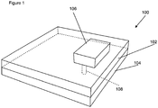
- FIG. 1 illustrates a sensor 100 according to an embodiment of the invention.
- the sensor has a silicon substrate 102. Coupled to a first surface of the silicon substrate 102 is integrated circuitry, which in this example is complementary metal oxide semiconductor (CMOS) circuitry 104. As shown in Figure 1 , the CMOS circuitry 104 is coupled to a bottom surface of the silicon substrate 102.
- CMOS complementary metal oxide semiconductor
- the sensor structure may be a comb structure, or any other type of sensor, including meanders, meander-combs or any other type of meander structure.
- the sensor structure 106 is in electronic communication with the CMOS circuitry 104 using a via 108 through the silicon substrate 102.
- vias or through silicon vias (TSVs) can be used to electrically couple components on different surfaces of a silicon substrate 102.
- a sensor structure 106 onto a silicon substrate 102 in accordance with embodiments of the invention can enable further functionality to be associated with a silicon substrate 102 without requiring an increase in the size of the silicon substrate 102 and/or a device/housing containing the silicon substrate 102.
- a radio frequency identification (RFID) integrated circuit/tag can have one or more sensors associated with its pre-existing silicon substrate without increasing the size of the silicon substrate 102, thereby avoiding an increase in the size of the integrated circuit/tag.
- RFID tag technology is being increasingly used for supply chain monitoring, and the integration of monitoring functions into the RFID technology, for example in order to monitor key environmental conditions such as for perishable products, can be seen as an advantage.
- the CMOS circuitry 104 can be used to store data received from the sensor structure 106, and/or perform one or more calculations on data, and/or wirelessly transmit the data obtained from sensors to a third party device.
- Particular advantages associated with using an embodiment of the invention with RFID technology can relate to the speed of operation of a logistics chain. For instance, one would not need to stop a container to find out what it contains or any environmental conditions inside the container, including any parameters that are erroneous. For example, there may not be a need to attach cables etc. to the container to determine information from within the container as may be required by the prior art. Simply driving the container through a scanning portal (or any similar RFID receiver/external source) would be sufficient to determine information sensed from within the container.
- a portal could be (for an end user) a refrigerator communicating with the RFID tags and providing an audible/visual warning whenever something is approaching the end of its lifetime or a limit (such as too much carbon dioxide, etc) is reached.
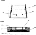
- Figures 2 to 7 illustrate the stages in the manufacture of a sensor according to an embodiment of the invention.
- Figures 2a and 2b illustrate a silicon substrate/wafer 202 having two vias 204. It will be appreciated that any number of vias 204 can be provided in accordance with the requirements of the CMOS circuitry and/or sensor structure 205, 205' that will be coupled to the vias 204.
- the vias 204 are exposed at a first surface 202a of the silicon substrate 202 and extend through the silicon substrate 202 towards a second surface 202b of the silicon substrate 202.
- the vias 204 are not exposed at the second surface 202b at this stage of manufacture and a layer of the silicon substrate 202 remains between the second surface 202b of the silicon substrate 202 and the end of the vias 204. That is, the vias 204 extend from the first surface 202a of the silicon substrate 202 towards the second surface 202b, but do not reach the second surface 202b.
- FIGs 3a and 3b show a second stage in the manufacture of the sensor.
- CMOS complementary metal oxide semiconductor
- IC integrated circuit
- Figures 4a and 4b show the next stage in the manufacture of the sensor.
- the silicon substrate 202 and CMOS circuitry 206 are shown upside down in Figures 4a and 4b with the second surface 202b of the silicon substrate 202 on top.
- Figures 4a and 4b show the silicon substrate 202 after it has been processed to expose the vias 204 on the second surface 202b of the silicon substrate 202.
- the silicon wafer 202 may be processed with a grinding and/or chemical mechanical planerization (CMP) operation in order to reduce the thickness of the silicon substrate 202 until the ends of the vias 204 that were previously enclosed by the silicon substrate 202 are exposed at the second surface 202b of the silicon substrate 202. That is, the silicon wafer 202 may be processed such that it is made thinner and its second surface 202b is pushed back until the vias 204 are exposed.
- CMP chemical mechanical planerization
- the grinding of the silicon may be considered as a coarse processing operation, and the CMP processing may be considered as a fine processing operation.
- CMP may be able to reduce the thickness of the silicon substrate 202 on a nanometer scale.
- Figure 5 shows the next stage in the manufacture of the sensor.
- a first part 208 of a sensor structure is coupled to the second surface 202b of the silicon substrate 202.
- the first part 208 of the sensor structure shown in Figure 5 consists of a double metal comb sensor structure.
- the metal/conductor 208 of the sensor structure may be deposited on the second surface 202b of the silicon substrate 202 and subsequently etched or otherwise processed in order to provide the desired shape. It will be appreciated that the metal structure 208 is deposited and etched so that it is in electrical communication with the other ends of the two vias 204 that are coupled to the CMOS circuitry 206 on the other side of the silicon 202.
- Figure 6 shows the next stage in the manufacture of the sensor.
- a sensor material 210 has been deposited on the second surface 202b of the silicon substrate 202 such that it surrounds the metal structure 208.
- a top surface of the sensor material 210 is substantially aligned with a top surface of the metal structure 208.
- suitable sensor materials can include polyimides, porous silicates, low-dielectric constant (K) materials, teflons and/or other gas/humidity sensing materials.
- the sensor material 210 may be deposited using a spin-on technique, whereby a liquid polymer is spun onto the surface 202b of the silicon substrate 202.
- the sensing material 210 may be deposited using chemical vapour deposition, or any other process.
- a sensor structure 205 may be considered as the metal structure 208 in combination with the sensor material 210. All of the components/materials shown in Figure 6 may be considered as a sensor according to an embodiment of the invention.
- FIG. 7 A further, optional, stage in the manufacture of the sensor is shown as Figure 7 .
- portions of the sensor material 210 that are not in the vicinity of the metal structure 208 have been removed.
- any portion of the sensor material 210 that is more than a certain distance from the metal structure 208 may be removed. Removal of the sensor material 210 in this way can expose further portions of the second surface 202b of the silicon substrate 202 for receiving further sensor structures, or receiving any other suitable components.
- Sensors according to embodiments of the invention may have any number of sensor structures provided on a second surface 202b of a silicon substrate 202.
- the sensor material 210 may be removed by lithography or etching, or any other known process.
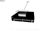
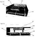
- Figure 8 and Figure 9 shows an alternative stage in the manufacture of a sensor according to an embodiment of the invention.
- the stages shown as Figures 8 and 9 can be seen as alternatives to the stages shown as Figures 6 and 7 in relation to the previous embodiment.
- the senor comprises a silicon substrate 302, having CMOS circuitry 306 coupled to its first surface 302a, and two vias 304 extending from the first surface 302a of the silicon substrate 302 to a second surface 302b of the silicon substrate 302. Coupled to the second surface 302b of the silicon substrate is a metal structure 308 that is similar to the metal structure 208 shown in Figures 5 to 7 .
- the sensor material 310 has been deposited on the second surface 302b of the silicon substrate 302 such that it also covers a top surface 308a of the metal structure 308.
- Providing the sensor material 310 such that it completely encloses all of the sides of the metal structure 308 that are not adjacent to the silicon substrate 302 can provide a sensor with a different sensitivity and speed of measurement when compared with the embodiment illustrated as Figures 6 and 7 .
- the sensor structure 305 comprises the conductor/metal 308 along with the sensor material 310.
- Figure 9 shows an optional further stage in the processing of a sensor according to an embodiment of the invention, whereby part of the sensor material 310 shown in Figure 8 has been removed in a similar way to that described in relation to Figure 7 .
- Figures 10 to 13 illustrate alternative stages in the manufacture of a sensor according to an embodiment of the invention, and can be seen as alternative stages to those described and illustrated in relation to Figures 4 to 7 above.
- Figures 10a and 10b show the silicon substrate 402 and CMOS circuitry 406 that are similar to the corresponding materials shown in Figures 3a and 3b , turned upside down such that the second surface 402b is shown on top.
- the silicon substrate 402 is then etched from its second surface 402b to define two trenches 412 that correspond to a double comb sensor structure shape.
- the silicon substrate 402 is etched away until the vias 404 are exposed at the bottom of the trenches 412. This operation may be referred to as backside lithography.
- the second surface 402b of the silicon substrate 402 can be considered as including the surfaces on the inside of the trenches 412, including the surfaces of the silicon substrate 402 at the bottom of the trenches 412.
- Figure 11 shows the next stage in the manufacture of the sensor.
- the trenches 412 that were etched and as shown in Figure 10 have been filled with a metal or doped polysilicon material 408 such that the metal 408 takes the shape of a double comb sensor structure. Any excess metal 408 that may be left above the level of the second surface 402b of the silicon substrate 402 may be removed.
- the sensor material 410 can be provided over the top of the metal structure 408, although doing so may reduce the sensitivity of the sensor structure because the silicon may act as a shield against the conditions that the sensor is to monitor.
- a metallised comb pattern is now provided in the silicon substrate 402.
- FIG 12 The next stage in the manufacture of the sensor is shown as Figure 12 , where the silicon substrate 402 surrounding the metal structure 408 has been etched away.
- the silicon substrate 402 in between the comb structure defined by the metal structure 408 is also etched away. Etching away the silicon substrate 402 in this way provides a further trench around and in between the metal structures 408.
- Figures 13a and 13b show the next stage in the manufacture of the sensor, whereby a sensor material has been provided to the further trench around the metal structure 408 such that the sensor material 410 can provide a suitable dielectric between the comb structure defined by the metal structures 408. It will be appreciated that the sensor material 410 can be similar to the sensor material 210 shown in Figures 6 and 7 .
- the sensor structure 405 consists of the metal/conductor 408 and sensor material 410 embedded in the silicon substrate 402.
- Figure 13b shows the sensor in cross section, where it can be seen that the vias 404 provide an electrical connection between the CMOS circuitry 406 on the first surface 402a of the silicon substrate 402, and a sensor structure provided by the sensor material 410 and metal structure 408 on the second surface 402b of the silicon substrate 402.
- Figure 14 shows a cross-sectional view of an embodiment of a sensor 500 according to an embodiment of the invention.
- the sensor is embodied as bumped and sawn dies, and Figure 14 shows the sensor 500 in cross section.
- the sensor 500 comprises a silicon substrate 502 having an integrated circuit (IC) 504 provided on a first surface of the silicon substrate 502 (the upper surface shown in Figure 14 ).
- the sensor 500 also comprises a sensor structure 506 provided on a second surface of the silicon substrate 502 (the lower surface shown in Figure 14 ).
- the IC 504 and sensor structure 506 are coupled by a through silicon via 508.
- Figure 15 shows another embodiment of a sensor according to the invention.
- the sensor 600 of Figure 15 is implemented as a flip-chip strap package.
- the senor 600 of Figure 15 is similar to the sensor 500 of Figure 14 and is "flip-chipped" onto an antenna 610.
- Features shown in Figure 15 that are common to features of Figure 14 are provided with corresponding reference number in the 600 series.
- FIG 16 shows a further embodiment of a sensor 700 according to the invention, and in this embodiment the sensor 700 is embodied as a standard dual in-line (DIL) package with a wire bonded die inside.
- DIL dual in-line
- One or more sensors described herein can be used for monitoring environmental conditions, such as in the vicinity of perishable products, and can be used to monitor one or more of: humidity content, gas concentrations (for example carbon dioxide, oxygen, hydrogen, ethylene, ammonia), pH, liquid emersion, light intensity, or any other environmental condition.
- gas concentrations for example carbon dioxide, oxygen, hydrogen, ethylene, ammonia
- pH for example carbon dioxide, oxygen, hydrogen, ethylene, ammonia
- liquid emersion for example carbon dioxide, oxygen, hydrogen, ethylene, ammonia
- Integrating such micro-sensors with CMOS IC technologies can decrease the cost of processing, and can provide an advantageous integrated solution in terms of area and power consumption.
- Figure 17 shows schematically the process flow according to a method of an embodiment of the invention.
- the method illustrated as Figure 17 is a method of manufacturing a sensor from a silicon wafer, and begins at step 702 by coupling CMOS circuitry to a first surface of a silicon wafer.
- the CMOS circuitry may be coupled to the silicon wafer in any known way.
- a sensor structure is coupled to a second surface of the silicon wafer. Examples of how a sensor structure could be coupled to the second surface of the silicon wafer are described above in relation to Figures 5 to 7 , 8 and 9 , and 10 to 13 .
- An electrical connection is provided between the sensor structure and the CMOS circuitry at step 706.
- the electrical connection may be provided by a through silicon via (TSV), or may be by any other means, for example by providing one or more wires around an edge of the silicon wafer.
- TSV through silicon via
Claims (8)
- Capteur (100) comprenant :un seul substrat de silicium (102 ; 202 ; 302 ; 402) ayant une première (202a ; 302a ; 402a) et une deuxième surface (202b ; 302b ; 402b) ;un circuit intégré (104 ; 206 ; 306 ; 406) sur la première surface (202a ; 302a ; 402a) du substrat de silicium (102 ; 202 ; 302 ; 402) ;une structure de capteur (106 ; 205 ; 305 ; 405) sur la deuxième surface (202b ; 302b ; 402b) du substrat de silicium (102 ; 202 ; 302 ; 402),dans lequel la structure de capteur (106 ; 205 ; 305 ; 405) et le circuit intégré (104 ; 206 ; 306 ; 406) sont couplés électriquement l'un à l'autre,caractérisé en ce quele capteur comprend en outre un ou plusieurs trous d'interconnexion (108 ; 204 ; 304 ; 404) s'étendant entre les première (202a ; 302a ; 402a) et deuxième (202b ; 302b ; 402b) surfaces du substrat de silicium (102 ; 202 ; 302 ; 402) et entre la structure de capteur (106 ; 205 ; 305 ; 405) et le circuit intégré (104 ; 206 ; 306 ; 406), et dans lequel le ou les trous d'interconnexion (108 ; 204 ; 304 ; 404) sont couplés électriquement au circuit intégré (104 ; 206 ; 306 ; 406) et à la structure de capteur (106 ; 205 ; 305 ; 405).
- Capteur de la revendication 1, dans lequel les zones des première (202a ; 302a ; 402a) et deuxième (202b ; 302b ; 402b) surfaces du substrat de silicium (102 ; 202 ; 302 ; 402) occupées par le circuit intégré (104 ; 206 ; 306 ; 406) et la structure de capteur (106 ; 205 ; 305 ; 405) se chevauchent.
- Capteur d'une quelconque revendication précédente, le capteur servant à détecter des conditions environnementales.
- Capteur d'une quelconque revendication précédente, dans lequel la structure de capteur (106 ; 205 ; 305 ; 405) comprend :un conducteur de capteur (208 ; 308 ; 408) couplé électriquement au circuit intégré (104 ; 206 ; 306 ; 406) ; etun matériau de capteur (210 ; 310 ; 410) adjacent à au moins une surface du conducteur de capteur (208 ; 308 ; 408).
- Capteur d'une quelconque revendication précédente, dans lequel la première surface (202a ; 302a ; 402a) et la deuxième surface (202b ; 302b ; 402b) du substrat de silicium (102 ; 202 ; 302 ; 402) sont des surfaces opposées.
- Capteur d'une quelconque revendication précédente, comprenant une pluralité de structures de capteur (106 ; 205 ; 305 ; 405) disposées sur la deuxième surface (202b ; 302b ; 402b) du substrat de silicium (102 ; 202 ; 302 ; 402).
- Étiquette d'identification radiofréquence comprenant le capteur d'une quelconque revendication précédente.
- Étiquette d'identification radiofréquence de la revendication 7, l'étiquette étant choisie dans le groupe comprenant :une puce pourvue de plots et découpée ;un boîtier câblé monté puce retournée ; etun boîtier double en ligne.
Priority Applications (2)
| Application Number | Priority Date | Filing Date | Title |
|---|---|---|---|
| EP09290734.4A EP2302327B1 (fr) | 2009-09-25 | 2009-09-25 | Capteur |
| US12/889,832 US9546884B2 (en) | 2009-09-25 | 2010-09-24 | Sensor |
Applications Claiming Priority (1)
| Application Number | Priority Date | Filing Date | Title |
|---|---|---|---|
| EP09290734.4A EP2302327B1 (fr) | 2009-09-25 | 2009-09-25 | Capteur |
Publications (2)
| Publication Number | Publication Date |
|---|---|
| EP2302327A1 EP2302327A1 (fr) | 2011-03-30 |
| EP2302327B1 true EP2302327B1 (fr) | 2020-02-26 |
Family
ID=42026786
Family Applications (1)
| Application Number | Title | Priority Date | Filing Date |
|---|---|---|---|
| EP09290734.4A Active EP2302327B1 (fr) | 2009-09-25 | 2009-09-25 | Capteur |
Country Status (2)
| Country | Link |
|---|---|
| US (1) | US9546884B2 (fr) |
| EP (1) | EP2302327B1 (fr) |
Families Citing this family (2)
| Publication number | Priority date | Publication date | Assignee | Title |
|---|---|---|---|---|
| EP2492239B1 (fr) | 2011-02-22 | 2020-08-26 | Sciosense B.V. | Circuit intégré avec capteur et procédé de fabrication d'un tel circuit intégré |
| KR101874839B1 (ko) | 2012-04-25 | 2018-07-05 | 이플러스이엘렉트로닉 게엠베하 | 습도 센서 장치 |
Citations (3)
| Publication number | Priority date | Publication date | Assignee | Title |
|---|---|---|---|---|
| WO2001080285A2 (fr) * | 2000-04-12 | 2001-10-25 | Honeywell International Inc. | Dispositifs optoelectroniques a eclairage vertical comportant des circuits integres micro-optiques et electroniques |
| EP2026082A2 (fr) * | 2007-08-14 | 2009-02-18 | Honeywell International Inc. | Puce à détection et à traitement intégrés double face |
| EP2060533A2 (fr) * | 2007-11-16 | 2009-05-20 | Hitachi Ltd. | Dispositif semi-conducteur et son procédé de fabrication |
Family Cites Families (12)
| Publication number | Priority date | Publication date | Assignee | Title |
|---|---|---|---|---|
| US6137151A (en) * | 1996-11-19 | 2000-10-24 | Xerox Corporation | Amorphous silicon sensor array with reduced number of address lines |
| WO2001084099A1 (fr) | 2000-05-04 | 2001-11-08 | Sensirion Ag | Module de detection et son procede de fabrication |
| JP2004518119A (ja) | 2001-01-10 | 2004-06-17 | ゼンジリオン アクチエンゲゼルシャフト | 伸張性コーティングを有するマイクロメカニカルフローセンサ |
| EP1738411A4 (fr) * | 2004-04-22 | 2012-06-27 | Panasonic Corp | Dispositif de capteur, système de capteur et procédés de fabrication de ceux-ci |
| US20060289981A1 (en) | 2005-06-28 | 2006-12-28 | Nickerson Robert M | Packaging logic and memory integrated circuits |
| US7255001B1 (en) | 2006-07-25 | 2007-08-14 | Honeywell International Inc. | Thermal fluid flow sensor and method of forming same technical field |
| EP1903000B1 (fr) * | 2006-09-25 | 2019-09-18 | Sorin CRM SAS | Composant biocompatible implantable incorporant un élément actif intégré tel qu'un capteur de mesure d'un paramètre physiologique, microsystème électromécanique ou circuit électronique |
| US8207853B2 (en) | 2008-01-14 | 2012-06-26 | Avery Dennison Corporation | Hybrid sensor/communication device, and method |
| EP2230507A1 (fr) | 2009-03-17 | 2010-09-22 | Nxp B.V. | Capteur d'humidité ou de gaz |
| EP2278309B1 (fr) | 2009-07-21 | 2019-05-15 | ams international AG | Capteur |
| EP2282333B1 (fr) * | 2009-07-27 | 2013-03-20 | Nxp B.V. | Circuit intégré avec capteur d'humidité |
| EP2343541A1 (fr) | 2009-12-22 | 2011-07-13 | Nxp B.V. | Capteur |
-
2009
- 2009-09-25 EP EP09290734.4A patent/EP2302327B1/fr active Active
-
2010
- 2010-09-24 US US12/889,832 patent/US9546884B2/en active Active
Patent Citations (3)
| Publication number | Priority date | Publication date | Assignee | Title |
|---|---|---|---|---|
| WO2001080285A2 (fr) * | 2000-04-12 | 2001-10-25 | Honeywell International Inc. | Dispositifs optoelectroniques a eclairage vertical comportant des circuits integres micro-optiques et electroniques |
| EP2026082A2 (fr) * | 2007-08-14 | 2009-02-18 | Honeywell International Inc. | Puce à détection et à traitement intégrés double face |
| EP2060533A2 (fr) * | 2007-11-16 | 2009-05-20 | Hitachi Ltd. | Dispositif semi-conducteur et son procédé de fabrication |
Also Published As
| Publication number | Publication date |
|---|---|
| US20110079649A1 (en) | 2011-04-07 |
| EP2302327A1 (fr) | 2011-03-30 |
| US9546884B2 (en) | 2017-01-17 |
Similar Documents
| Publication | Publication Date | Title |
|---|---|---|
| EP2328173B1 (fr) | Batterie intégrée et circuit intégré | |
| US20140070337A1 (en) | Integrated circuit including an environmental sensor | |
| JP5557960B2 (ja) | 無線で接続されたチップ上の流体センサ | |
| EP2656057B1 (fr) | Composant électronique integré pour surveiller des paramètres dans une construction en dur et système de surveillance utilisant un tel composant | |
| CN105226035B (zh) | 晶片封装体 | |
| US9487392B2 (en) | Method of packaging integrated circuits and a molded package | |
| CN104136365A (zh) | 用于在集成板中嵌入受控腔mems封装的方法 | |
| CN107748230B (zh) | 具有框架通路的气体传感器设备和相关方法 | |
| US9355975B2 (en) | Chip package and method for forming the same | |
| US8264074B2 (en) | Device for use as dual-sided sensor package | |
| EP3001186B1 (fr) | Puce de capteur | |
| CN104620086A (zh) | 具有至少两个用于探测电磁辐射的晶片的装置及用于制造该装置的方法 | |
| KR20180049797A (ko) | 언더 스크린 센서 어셈블리 | |
| CN102832180B (zh) | 晶片封装体及其形成方法 | |
| CN103985683A (zh) | 晶片封装体 | |
| US20100078832A1 (en) | Sensor node module | |
| EP2302327B1 (fr) | Capteur | |
| KR20170039700A (ko) | 센서 | |
| US11372176B2 (en) | Implantable optical sensor with hermetically sealed cover cap | |
| CN206767639U (zh) | 集成半导体器件 | |
| CN105789149A (zh) | 传感器组件 | |
| CN103187379B (zh) | 半导体堆栈结构及其制法 | |
| US8866239B2 (en) | IC manufacturing method, IC and apparatus | |
| KR20130046470A (ko) | 압력센서용 멤스 디바이스 | |
| WO2011053110A2 (fr) | Capteur environnemental intégré et puce roic et procédé de fabrication associé |
Legal Events
| Date | Code | Title | Description |
|---|---|---|---|
| PUAI | Public reference made under article 153(3) epc to a published international application that has entered the european phase |
Free format text: ORIGINAL CODE: 0009012 |
|
| AK | Designated contracting states |
Kind code of ref document: A1 Designated state(s): AT BE BG CH CY CZ DE DK EE ES FI FR GB GR HR HU IE IS IT LI LT LU LV MC MK MT NL NO PL PT RO SE SI SK SM TR |
|
| AX | Request for extension of the european patent |
Extension state: AL BA RS |
|
| 17P | Request for examination filed |
Effective date: 20110930 |
|
| 17Q | First examination report despatched |
Effective date: 20130805 |
|
| STAA | Information on the status of an ep patent application or granted ep patent |
Free format text: STATUS: EXAMINATION IS IN PROGRESS |
|
| GRAP | Despatch of communication of intention to grant a patent |
Free format text: ORIGINAL CODE: EPIDOSNIGR1 |
|
| STAA | Information on the status of an ep patent application or granted ep patent |
Free format text: STATUS: GRANT OF PATENT IS INTENDED |
|
| INTG | Intention to grant announced |
Effective date: 20191112 |
|
| GRAS | Grant fee paid |
Free format text: ORIGINAL CODE: EPIDOSNIGR3 |
|
| GRAA | (expected) grant |
Free format text: ORIGINAL CODE: 0009210 |
|
| STAA | Information on the status of an ep patent application or granted ep patent |
Free format text: STATUS: THE PATENT HAS BEEN GRANTED |
|
| AK | Designated contracting states |
Kind code of ref document: B1 Designated state(s): AT BE BG CH CY CZ DE DK EE ES FI FR GB GR HR HU IE IS IT LI LT LU LV MC MK MT NL NO PL PT RO SE SI SK SM TR |
|
| REG | Reference to a national code |
Ref country code: GB Ref legal event code: FG4D |
|
| REG | Reference to a national code |
Ref country code: CH Ref legal event code: EP |
|
| REG | Reference to a national code |
Ref country code: AT Ref legal event code: REF Ref document number: 1238188 Country of ref document: AT Kind code of ref document: T Effective date: 20200315 |
|
| REG | Reference to a national code |
Ref country code: IE Ref legal event code: FG4D |
|
| REG | Reference to a national code |
Ref country code: DE Ref legal event code: R096 Ref document number: 602009061264 Country of ref document: DE |
|
| PG25 | Lapsed in a contracting state [announced via postgrant information from national office to epo] |
Ref country code: NO Free format text: LAPSE BECAUSE OF FAILURE TO SUBMIT A TRANSLATION OF THE DESCRIPTION OR TO PAY THE FEE WITHIN THE PRESCRIBED TIME-LIMIT Effective date: 20200526 Ref country code: FI Free format text: LAPSE BECAUSE OF FAILURE TO SUBMIT A TRANSLATION OF THE DESCRIPTION OR TO PAY THE FEE WITHIN THE PRESCRIBED TIME-LIMIT Effective date: 20200226 |
|
| REG | Reference to a national code |
Ref country code: NL Ref legal event code: MP Effective date: 20200226 |
|
| REG | Reference to a national code |
Ref country code: LT Ref legal event code: MG4D |
|
| PG25 | Lapsed in a contracting state [announced via postgrant information from national office to epo] |
Ref country code: GR Free format text: LAPSE BECAUSE OF FAILURE TO SUBMIT A TRANSLATION OF THE DESCRIPTION OR TO PAY THE FEE WITHIN THE PRESCRIBED TIME-LIMIT Effective date: 20200527 Ref country code: LV Free format text: LAPSE BECAUSE OF FAILURE TO SUBMIT A TRANSLATION OF THE DESCRIPTION OR TO PAY THE FEE WITHIN THE PRESCRIBED TIME-LIMIT Effective date: 20200226 Ref country code: IS Free format text: LAPSE BECAUSE OF FAILURE TO SUBMIT A TRANSLATION OF THE DESCRIPTION OR TO PAY THE FEE WITHIN THE PRESCRIBED TIME-LIMIT Effective date: 20200626 Ref country code: SE Free format text: LAPSE BECAUSE OF FAILURE TO SUBMIT A TRANSLATION OF THE DESCRIPTION OR TO PAY THE FEE WITHIN THE PRESCRIBED TIME-LIMIT Effective date: 20200226 Ref country code: HR Free format text: LAPSE BECAUSE OF FAILURE TO SUBMIT A TRANSLATION OF THE DESCRIPTION OR TO PAY THE FEE WITHIN THE PRESCRIBED TIME-LIMIT Effective date: 20200226 Ref country code: BG Free format text: LAPSE BECAUSE OF FAILURE TO SUBMIT A TRANSLATION OF THE DESCRIPTION OR TO PAY THE FEE WITHIN THE PRESCRIBED TIME-LIMIT Effective date: 20200526 |
|
| PG25 | Lapsed in a contracting state [announced via postgrant information from national office to epo] |
Ref country code: NL Free format text: LAPSE BECAUSE OF FAILURE TO SUBMIT A TRANSLATION OF THE DESCRIPTION OR TO PAY THE FEE WITHIN THE PRESCRIBED TIME-LIMIT Effective date: 20200226 |
|
| PG25 | Lapsed in a contracting state [announced via postgrant information from national office to epo] |
Ref country code: DK Free format text: LAPSE BECAUSE OF FAILURE TO SUBMIT A TRANSLATION OF THE DESCRIPTION OR TO PAY THE FEE WITHIN THE PRESCRIBED TIME-LIMIT Effective date: 20200226 Ref country code: RO Free format text: LAPSE BECAUSE OF FAILURE TO SUBMIT A TRANSLATION OF THE DESCRIPTION OR TO PAY THE FEE WITHIN THE PRESCRIBED TIME-LIMIT Effective date: 20200226 Ref country code: SK Free format text: LAPSE BECAUSE OF FAILURE TO SUBMIT A TRANSLATION OF THE DESCRIPTION OR TO PAY THE FEE WITHIN THE PRESCRIBED TIME-LIMIT Effective date: 20200226 Ref country code: EE Free format text: LAPSE BECAUSE OF FAILURE TO SUBMIT A TRANSLATION OF THE DESCRIPTION OR TO PAY THE FEE WITHIN THE PRESCRIBED TIME-LIMIT Effective date: 20200226 Ref country code: SM Free format text: LAPSE BECAUSE OF FAILURE TO SUBMIT A TRANSLATION OF THE DESCRIPTION OR TO PAY THE FEE WITHIN THE PRESCRIBED TIME-LIMIT Effective date: 20200226 Ref country code: PT Free format text: LAPSE BECAUSE OF FAILURE TO SUBMIT A TRANSLATION OF THE DESCRIPTION OR TO PAY THE FEE WITHIN THE PRESCRIBED TIME-LIMIT Effective date: 20200719 Ref country code: LT Free format text: LAPSE BECAUSE OF FAILURE TO SUBMIT A TRANSLATION OF THE DESCRIPTION OR TO PAY THE FEE WITHIN THE PRESCRIBED TIME-LIMIT Effective date: 20200226 Ref country code: CZ Free format text: LAPSE BECAUSE OF FAILURE TO SUBMIT A TRANSLATION OF THE DESCRIPTION OR TO PAY THE FEE WITHIN THE PRESCRIBED TIME-LIMIT Effective date: 20200226 Ref country code: ES Free format text: LAPSE BECAUSE OF FAILURE TO SUBMIT A TRANSLATION OF THE DESCRIPTION OR TO PAY THE FEE WITHIN THE PRESCRIBED TIME-LIMIT Effective date: 20200226 |
|
| REG | Reference to a national code |
Ref country code: AT Ref legal event code: MK05 Ref document number: 1238188 Country of ref document: AT Kind code of ref document: T Effective date: 20200226 |
|
| REG | Reference to a national code |
Ref country code: DE Ref legal event code: R097 Ref document number: 602009061264 Country of ref document: DE |
|
| PLBE | No opposition filed within time limit |
Free format text: ORIGINAL CODE: 0009261 |
|
| STAA | Information on the status of an ep patent application or granted ep patent |
Free format text: STATUS: NO OPPOSITION FILED WITHIN TIME LIMIT |
|
| PG25 | Lapsed in a contracting state [announced via postgrant information from national office to epo] |
Ref country code: IT Free format text: LAPSE BECAUSE OF FAILURE TO SUBMIT A TRANSLATION OF THE DESCRIPTION OR TO PAY THE FEE WITHIN THE PRESCRIBED TIME-LIMIT Effective date: 20200226 Ref country code: AT Free format text: LAPSE BECAUSE OF FAILURE TO SUBMIT A TRANSLATION OF THE DESCRIPTION OR TO PAY THE FEE WITHIN THE PRESCRIBED TIME-LIMIT Effective date: 20200226 |
|
| 26N | No opposition filed |
Effective date: 20201127 |
|
| PG25 | Lapsed in a contracting state [announced via postgrant information from national office to epo] |
Ref country code: SI Free format text: LAPSE BECAUSE OF FAILURE TO SUBMIT A TRANSLATION OF THE DESCRIPTION OR TO PAY THE FEE WITHIN THE PRESCRIBED TIME-LIMIT Effective date: 20200226 Ref country code: PL Free format text: LAPSE BECAUSE OF FAILURE TO SUBMIT A TRANSLATION OF THE DESCRIPTION OR TO PAY THE FEE WITHIN THE PRESCRIBED TIME-LIMIT Effective date: 20200226 |
|
| PG25 | Lapsed in a contracting state [announced via postgrant information from national office to epo] |
Ref country code: MC Free format text: LAPSE BECAUSE OF FAILURE TO SUBMIT A TRANSLATION OF THE DESCRIPTION OR TO PAY THE FEE WITHIN THE PRESCRIBED TIME-LIMIT Effective date: 20200226 |
|
| REG | Reference to a national code |
Ref country code: CH Ref legal event code: PL |
|
| GBPC | Gb: european patent ceased through non-payment of renewal fee |
Effective date: 20200925 |
|
| REG | Reference to a national code |
Ref country code: BE Ref legal event code: MM Effective date: 20200930 |
|
| PG25 | Lapsed in a contracting state [announced via postgrant information from national office to epo] |
Ref country code: LU Free format text: LAPSE BECAUSE OF NON-PAYMENT OF DUE FEES Effective date: 20200925 |
|
| PG25 | Lapsed in a contracting state [announced via postgrant information from national office to epo] |
Ref country code: BE Free format text: LAPSE BECAUSE OF NON-PAYMENT OF DUE FEES Effective date: 20200930 Ref country code: CH Free format text: LAPSE BECAUSE OF NON-PAYMENT OF DUE FEES Effective date: 20200930 Ref country code: LI Free format text: LAPSE BECAUSE OF NON-PAYMENT OF DUE FEES Effective date: 20200930 Ref country code: GB Free format text: LAPSE BECAUSE OF NON-PAYMENT OF DUE FEES Effective date: 20200925 Ref country code: IE Free format text: LAPSE BECAUSE OF NON-PAYMENT OF DUE FEES Effective date: 20200925 |
|
| PG25 | Lapsed in a contracting state [announced via postgrant information from national office to epo] |
Ref country code: TR Free format text: LAPSE BECAUSE OF FAILURE TO SUBMIT A TRANSLATION OF THE DESCRIPTION OR TO PAY THE FEE WITHIN THE PRESCRIBED TIME-LIMIT Effective date: 20200226 Ref country code: MT Free format text: LAPSE BECAUSE OF FAILURE TO SUBMIT A TRANSLATION OF THE DESCRIPTION OR TO PAY THE FEE WITHIN THE PRESCRIBED TIME-LIMIT Effective date: 20200226 Ref country code: CY Free format text: LAPSE BECAUSE OF FAILURE TO SUBMIT A TRANSLATION OF THE DESCRIPTION OR TO PAY THE FEE WITHIN THE PRESCRIBED TIME-LIMIT Effective date: 20200226 |
|
| PG25 | Lapsed in a contracting state [announced via postgrant information from national office to epo] |
Ref country code: MK Free format text: LAPSE BECAUSE OF FAILURE TO SUBMIT A TRANSLATION OF THE DESCRIPTION OR TO PAY THE FEE WITHIN THE PRESCRIBED TIME-LIMIT Effective date: 20200226 |
|
| P01 | Opt-out of the competence of the unified patent court (upc) registered |
Effective date: 20230724 |
|
| PGFP | Annual fee paid to national office [announced via postgrant information from national office to epo] |
Ref country code: FR Payment date: 20230822 Year of fee payment: 15 Ref country code: DE Payment date: 20230822 Year of fee payment: 15 |