EP2297752B1 - Transformateur ainsi que élément de culot de lampe, culot de lampe et lampe à décharge avec un culot de lampe de ce type - Google Patents
Transformateur ainsi que élément de culot de lampe, culot de lampe et lampe à décharge avec un culot de lampe de ce type Download PDFInfo
- Publication number
- EP2297752B1 EP2297752B1 EP09779942.3A EP09779942A EP2297752B1 EP 2297752 B1 EP2297752 B1 EP 2297752B1 EP 09779942 A EP09779942 A EP 09779942A EP 2297752 B1 EP2297752 B1 EP 2297752B1
- Authority
- EP
- European Patent Office
- Prior art keywords
- transformer
- lamp base
- contact
- lamp
- base element
- Prior art date
- Legal status (The legal status is an assumption and is not a legal conclusion. Google has not performed a legal analysis and makes no representation as to the accuracy of the status listed.)
- Not-in-force
Links
Images


Classifications
-
- H—ELECTRICITY
- H01—ELECTRIC ELEMENTS
- H01F—MAGNETS; INDUCTANCES; TRANSFORMERS; SELECTION OF MATERIALS FOR THEIR MAGNETIC PROPERTIES
- H01F38/00—Adaptations of transformers or inductances for specific applications or functions
- H01F38/12—Ignition, e.g. for IC engines
-
- H—ELECTRICITY
- H01—ELECTRIC ELEMENTS
- H01F—MAGNETS; INDUCTANCES; TRANSFORMERS; SELECTION OF MATERIALS FOR THEIR MAGNETIC PROPERTIES
- H01F5/00—Coils
- H01F5/04—Arrangements of electric connections to coils, e.g. leads
-
- H—ELECTRICITY
- H05—ELECTRIC TECHNIQUES NOT OTHERWISE PROVIDED FOR
- H05B—ELECTRIC HEATING; ELECTRIC LIGHT SOURCES NOT OTHERWISE PROVIDED FOR; CIRCUIT ARRANGEMENTS FOR ELECTRIC LIGHT SOURCES, IN GENERAL
- H05B41/00—Circuit arrangements or apparatus for igniting or operating discharge lamps
- H05B41/02—Details
-
- F—MECHANICAL ENGINEERING; LIGHTING; HEATING; WEAPONS; BLASTING
- F21—LIGHTING
- F21S—NON-PORTABLE LIGHTING DEVICES; SYSTEMS THEREOF; VEHICLE LIGHTING DEVICES SPECIALLY ADAPTED FOR VEHICLE EXTERIORS
- F21S41/00—Illuminating devices specially adapted for vehicle exteriors, e.g. headlamps
- F21S41/10—Illuminating devices specially adapted for vehicle exteriors, e.g. headlamps characterised by the light source
- F21S41/14—Illuminating devices specially adapted for vehicle exteriors, e.g. headlamps characterised by the light source characterised by the type of light source
- F21S41/17—Discharge light sources
-
- F—MECHANICAL ENGINEERING; LIGHTING; HEATING; WEAPONS; BLASTING
- F21—LIGHTING
- F21S—NON-PORTABLE LIGHTING DEVICES; SYSTEMS THEREOF; VEHICLE LIGHTING DEVICES SPECIALLY ADAPTED FOR VEHICLE EXTERIORS
- F21S41/00—Illuminating devices specially adapted for vehicle exteriors, e.g. headlamps
- F21S41/10—Illuminating devices specially adapted for vehicle exteriors, e.g. headlamps characterised by the light source
- F21S41/19—Attachment of light sources or lamp holders
- F21S41/192—Details of lamp holders, terminals or connectors
-
- F—MECHANICAL ENGINEERING; LIGHTING; HEATING; WEAPONS; BLASTING
- F21—LIGHTING
- F21V—FUNCTIONAL FEATURES OR DETAILS OF LIGHTING DEVICES OR SYSTEMS THEREOF; STRUCTURAL COMBINATIONS OF LIGHTING DEVICES WITH OTHER ARTICLES, NOT OTHERWISE PROVIDED FOR
- F21V23/00—Arrangement of electric circuit elements in or on lighting devices
- F21V23/02—Arrangement of electric circuit elements in or on lighting devices the elements being transformers, impedances or power supply units, e.g. a transformer with a rectifier
- F21V23/026—Fastening of transformers or ballasts
-
- Y—GENERAL TAGGING OF NEW TECHNOLOGICAL DEVELOPMENTS; GENERAL TAGGING OF CROSS-SECTIONAL TECHNOLOGIES SPANNING OVER SEVERAL SECTIONS OF THE IPC; TECHNICAL SUBJECTS COVERED BY FORMER USPC CROSS-REFERENCE ART COLLECTIONS [XRACs] AND DIGESTS
- Y02—TECHNOLOGIES OR APPLICATIONS FOR MITIGATION OR ADAPTATION AGAINST CLIMATE CHANGE
- Y02B—CLIMATE CHANGE MITIGATION TECHNOLOGIES RELATED TO BUILDINGS, e.g. HOUSING, HOUSE APPLIANCES OR RELATED END-USER APPLICATIONS
- Y02B20/00—Energy efficient lighting technologies, e.g. halogen lamps or gas discharge lamps
Definitions
- the invention relates to a lamp base element with a transformer according to the preamble of patent claim 1, a lamp base with such a lamp base element and a discharge lamp with such a lamp base.
- the EP 1 511 131 A1 discloses a transformer housed in a lamp cap for a high pressure discharge lamp.
- the transformer has a primary winding wound around a transformer housing with the winding terminals facing away from the transformer housing.
- a secondary winding of the transformer is disposed within the transformer housing, the winding outlets are led through the transformer housing to the outside.
- the disadvantage here is that the winding outlets of the primary and secondary windings of the transformer have a low mechanical rigidity and therefore are expensive to protect against external mechanical influences, mounted in the lamp base, for example in so-called transformer trays before mounting.
- Another disadvantage is the high material costs, since the entire lamp base and the transformer, because of the high temperatures occurring during operation of the high-pressure discharge lamp, consist of a high-temperature-resistant and cost-intensive plastic.
- the DE 195 21 070 A1 discloses a high voltage transformer and a discharge lamp circuit.
- the high voltage transformer has a core, a primary winding, a secondary winding, a base plate and insulating material covering the core and the secondary winding, and a conductive holder serving as a primary winding.
- the DE 10 2006 014 695 A1 describes a method for producing an electrically insulating potting body and a base for a lamp.
- the object of the present invention is to provide a lamp base element, a lamp cap and a discharge lamp, which are inexpensive to manufacture and robust against external influences.
- the transformer of the lamp base element according to the invention for mounting in a lamp base has a transformer housing which encloses a transformer core provided with a first winding. Around the transformer housing around a second winding is arranged, which is advantageously fixed with at least one contact element to the transformer housing.
- This solution has the advantage that the transformer has a high mechanical strength, in particular with respect to the second winding, whereby the transformer can be pourable.
- the contact element is formed as in a AufEnglishung of the transformer housing preferably self-locking recorded contact pin.
- the second winding of the transformer can be mechanically fixed and electrically contacted, for example, by two contact pins. As a result, the second winding of the transformer is easy to fix and very robust.
- the second winding can be designed as a ribbon winding and have at respective winding ends FixierausEnglishept through which the contact pins are guided.
- a ribbon winding is easy to manufacture and can be mounted on the transformer.
- the contact pins in each case approximately centrally have a clamping collar and the ribbon winding between the clamping collar and the transformer housing is arranged, whereby the ribbon winding is set mechanically extremely robust.
- the transformer housing has an approximately elliptical cross-section, wherein the length of the transformer housing is greater than the maximum height.
- the contact pins may face radially outward in the same direction from the main apex of the transformer housing.
- a lamp base element for receiving a transformer.
- This solution has the advantage that the lamp base element and the transformer are substantially mechanically decoupled from a lamp base as a separate component, and can be produced, for example, from a less expensive plastic having a higher coefficient of thermal expansion.
- the lamp base element to protect the transformer has a fully accommodating the transformer transformer chamber.
- the contact pins of the transformer are guided through an opening side opposite the contacting side of the transformer chamber to allow easy contact, for example with a circuit board.
- a center contact element in the transformer chamber is introduced so that a transformer contact region of the center contact element for contacting the guided out of the transformer housing first winding of the transformer within and a lamp contact region of the center contact element, in particular for contacting a high-pressure discharge lamp, outside the transformer chamber is arranged ,
- For electrical insulation can advantageously be a chamber interior of the transformer chamber of the lamp base element after receiving the transformer to be poured with a potting material.
- the casting material is for example a cost-effective silicone rubber.
- the transformer chamber advantageously has a lateral surface delimiting the opening side, which has two longitudinal sides and two transverse sides, wherein the sides are arranged substantially rectangular relative to one another.
- the lamp contact region of the center contact element is accommodated in a center contact ring, which is formed centrally in the longitudinal direction of the longitudinal side of the transformer chamber on the longitudinal side, that a ring axis of the center contact ring extends approximately parallel to the contact pins of the transformer and a ring top of the center contact ring in approximately flush with the opening side of the transformer chamber.
- the transformer can be easily contacted with, for example, a high-pressure discharge lamp when installing the lamp base element in the lamp base.
- a funnel can be formed approximately centrally of the center contact ring, which tapers along the ring axis in the direction of the surface normal of the opening side pointing away from the transformer chamber to the lamp contact region of the center contact element.
- the center contact ring on a ring underside forms an annular spring and a ring having a larger radius than the ring spring energy directors each for connection to a lamp base out.
- the energy directing device can be used for simple ultrasonic welding of the lamp base element to the lamp base.
- the contact pins can be connected from the outside with contact plates, which provide a flat contacting possibilities with, for example, a printed circuit board.
- the contact plates protrude in each case in sections in the longitudinal direction of the transformer chamber to the outside and can thus be easily welded, for example, with other elements in this area.
- the contact plates can each be bounded in sections by the transverse side of the lateral surface of protruding fixing elements, which can serve as protection, for example during assembly of the lamp base element with the lamp cap.
- At least one dowel pin may be formed on the contacting side of the lamp cap element.
- a lamp base in particular for receiving a high-pressure discharge lamp, has a carrier plate.
- a cylindrical middle dome may be formed on a carrier side of the carrier plate facing away from the high-pressure discharge lamp.
- the lamp base element with the ring underside rests approximately on a middle dome head side and is fixed to the middle dome.
- a socket can be inexpensively formed integrally on the side of the carrier plate partially surrounding lateral surface portion.
- the cylindrical central dome preferably extends through a board recess of the board.
- the contact plates of the lamp base element can be electrically and mechanically connected to the circuit board simply.
- the central dome can, for example, have a power supply channel which opens into the funnel of the lamp base element in order, for example, to connect a power supply line of the high-pressure discharge lamp introduced into the power supply channel to the center contact element of the lamp base element.
- the lamp cap may be enclosed with a socket lid, wherein the socket lid forms an annular spring and an annular energy directors, which are each immersed in an annular groove of the lamp cap member. Through the ring spring and the energy directors, the base cap can be easily connected to the lamp base.
- circuit board has expansion joints in the region of the contact pins of the lamp base element, as a result of which volume changes of the circuit board and / or of the lamp base element can be easily compensated due to temperature fluctuations.
- At least one dowel pin of the lamp cap element dives into at least one pin receptacle of the board.
- An easily produced inventive discharge lamp has the lamp base described above.
- FIG. 1 shows a side view of a high-pressure discharge lamp 1 according to a preferred embodiment, which is preferably used for a motor vehicle headlight.
- This has a discharge vessel 4 made of quartz glass surrounded by a glass outer bulb 2 and having electrodes 6, 8 arranged therein for generating a gas discharge.
- the electrodes 6 and 8 are each connected to a guided out of the discharge vessel 4 out power supply 10 and 12 for supplying electrical energy.
- the outer bulb 2 and the discharge vessel 4 are attached to a lamp cap 14, which with a in the FIG. 1 not shown lamp base element, in which a transformer is introduced, is formed.
- FIG. 2 shows the lamp cap 14 off FIG. 1 according to the embodiment quasi upside down, the lamp cap 14 is shown without a base cover.
- the lamp base 14 forms at its in FIG. 2 lower base side 16 a reference ring 18 with downwardly projecting retaining lugs 20 for fixing the position of the high-pressure discharge lamp 1 from FIG. 1 out.
- the reference ring 18 is connected via a cylindrical web 22 on the holding lugs 20 opposite side with a support plate 24 of the lamp cap 14.
- the carrier plate 24 has on its side facing away from the reference ring 18 carrier side 26 has an approximately centrally disposed cylindrical central dome 28 which extends substantially along the base longitudinal axis 30.
- a lamp base element or base element 32 which in the following FIG. 3 is explained in more detail, is connected via a formed on the base member 32 center contact ring 34 with a dome face 36 of the central dome 28.
- the support plate 24 has an approximately rectangular circumference, wherein at one in the FIG. 2 left lateral surface portion 40 of the lamp cap 14, a female connector 42 for electrical contacting of the high-pressure discharge lamp 1 is integrally formed.
- the socket 42 projects thereby approximately at the height of the center contact ring 34 of the base member 32 to the outside.
- a plug receptacle of the socket 42 is of the in FIG. 2 left end face 44 of the socket 42 accessible.
- contact pins 46, 48 are embedded, which extend from the socket 42 on the lateral surface portion 40 and the support plate 24 and approximately between the lateral surface portion 40 and the central dome 28 protrude from the support side 26 of the support plate 24 substantially parallel to the base longitudinal axis 30.
- the wire lengths of the contact pins can be different overall, so that the in FIG. 2 right contact pin 48, for example, a greater distance from the lateral surface portion 40 has.
- a lead frame or a circuit board 50 is arranged. This has two not visible in this figure recesses through which the contact pins 46, 48 are guided through and thus between the board 50 and the contact pins 46, 48, a so-called pin-in-hole connection is performed.
- the contact pins 46, 48 are either self-locking introduced into the recesses of the board 50 or are additionally welded to the circuit board 50, for example.
- the board 50 has in the middle of a not visible in this figure recess area through which the central dome 28 is guided.
- the board 50 is fixed in position by the base member 32, which is explained in more detail below in the following figures.
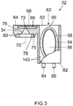
- FIG. 3 shows the base member 32 according to the embodiment in a side view, with parts of the drawing are shown in an outbreak diagram.
- a transformer chamber 52 of the base member 32 a transformer 54 is completely received.
- the transformer 54 has a transformer core 56 wrapped by a first winding 58, the secondary winding 58 and the transformer core 56 are enclosed by a transformer housing 60 having an approximately elliptical cross-section.
- the transformer 60 is converted into an in FIG. 3 overhead opening side 62 of the transformer chamber 52 introduced.
- the opening side lies approximately in the same plane as a ring top side 64 of the center contact ring 34 of the base element 32.
- a center contact element 66 for making electrical contact with the high-pressure discharge lamp 1 FIG. 1 and the transformer 54 is embedded in the base element 32 in such a way that a transformer contact region of the center contact element 66, not shown in this figure, contacts the transformer 54 and the lamp contact region 68 of the center contact element 66 in the center contact ring 34 for contacting the secondary winding 58 of the transformer 54 inside the transformer chamber 52 is arranged.
- the arrangement of the center contact element 66 will be explained in more detail in the figures described below.
- the center contact ring 34 is in the region of the lamp contact region 68 of the center contact element 66 for welding to the power supply 10 of the high-pressure discharge lamp 1 from FIG. 1 towards the ring top 64 open.
- the lamp contact region 68 of the center contact element 66 also has to carry out the power supply 10 from FIG. 1 a through opening 72 extending along a ring axis 70 of the center contact ring 34.
- In the passage opening 72 opens from a ring bottom 75 along the ring axis 70 extending and to the through hole 72 toward tapering funnel 76.
- the funnel 76 is used for easy recording of the power supply 10 from FIG. 1 during assembly of the high pressure discharge lamp 1.
- annular spring 78 extending around the ring axis 70 and an annular energy directing device 80 having a larger diameter are formed with a pointed cross-section.
- the energy director 80 is used for ultrasonic welding.
- One of the opening side 62 of the transformer chamber 52 opposite contacting side 82 has two down in FIG. 3 cantilevered and mutually offset dowel pins 84, 86, a fixing of the base member 32 on the board 50 in FIG. 2 support.
- the base element 32 from the FIG. 3 is a plastic injection molded component of polyphenylene sulfide (PPS).
- PPS polyphenylene sulfide
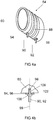
- FIG. 4a shows the transformer 54 in a perspective view.
- a ribbon winding of copper surrounding the transformer housing 60 serves as a second winding or as a primary winding 88 of the transformer 54.
- a round wire would also be conceivable as a primary winding 88.
- the elliptical cross-section transformer housing 60 has a length which is greater than the maximum height.
- Two contact pins 90, 92 collar of one Main vertex of the transformer housing 60 radially outward in a common direction, wherein the contact pins 90 and 92 each define a winding end 94 and 96 of the primary winding 88 on the transformer housing 60 and electrically contact.
- FIG. 4b is a coil end 94, 96 with a contact pin 90, 92 made FIG. 4a enlarged shown in a cross-sectional view.
- the contact pins 90, 92 are used in pin recesses 98 of the transformer housing 60, for example, self-locking by means of a press fit or by gluing.
- a clamping collar 100 is formed, which has an approximately flat and the PinlHarsachse 99 of the contact pins 90, 92 vertically formed clamping surface 102.
- the winding ends 94, 96 of the primary winding 88 are respectively clamped.
- the winding ends 94, 96 each have a through opening 106, through which the respective contact pin 90 and 92 is passed.
- the coil ends 94 and 96 may be soldered to the respective contact pins 90 and 92, respectively.
- the winding ends 94, 96 and thus the primary winding 88 are thus fixed by the contact pins 90, 92 force, material and / or positive and electrically contacted. In this way, the primary winding 88 can be wound in the manufacturing process with a lower accuracy compared to the prior art, since a fixation of the primary winding 88 on the transformer housing 60, which is carried out solely by the winding, is no longer necessary.
- the primary winding 88 is through the contact pins 90, 92 extremely robust and has a high mechanical strength, whereby the transformer 54 is bulk material capable and not, as in the prior art, must be included for protection in so-called transformer trays, which cause high additional costs, since on the one hand consuming equipped with transformers and on the other hand must be regularly subjected to a cleaning to remove dust and material residues. Due to the bulk material capability of the transformer 54 transport and storage costs are significantly reduced compared to the prior art, the handling in the manufacturing process is simplified and the manufacture and assembly is safer.
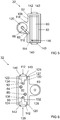
- FIG. 5 shows the base member 32 in a plan view in the direction of the opening side 62 FIG. 3 according to the embodiment.
- the tongue-shaped lamp contact region 68 of the center contact element 66 extends in the FIG. 5 approximately obliquely down to a longitudinal side 108 of the transformer chamber 52, on which the center contact ring 34 is formed.
- a center section 110 of the center contact element 66 is embedded substantially in the longitudinal side 108 and extends up to one in FIG. 5 the lower transverse side 112 of the transformer chamber 52.
- the center contact element 66 projects on the longitudinal side 108 with a transformer contact region 114 approximately along the transverse side 112 into the transformer chamber 52.
- a winding end 116 of the secondary winding 58 (see FIG. 3 ), out led to the transformer housing 60 and is electrically connected to the transformer contact area 114, for example in the form of a weld.
- the center contact element 66 consists for example of X5CrNi1810 and is integrated as an insert into the base element 32 produced by plastic injection molding.
- the center contact ring 34 is formed substantially centrally in the longitudinal direction of the longitudinal side 108 of the transformer chamber 52.
- the connecting region of the center contact ring 34 with the longitudinal side 108 is reinforced via a connecting web 118.
- the longitudinal side 108 of the transformer chamber 52 is widened in the region of the center section 110 of the center contact element 66 in order to sufficiently embed the center contact element 66.
- the center contact ring 34 has a circular inner portion 120 stepped back from the ring top 64, whereby the lamp contact area 68 of the center contact element 66 is exposed.
- FIG. 6 shows a bottom view of the base member 32 according to the embodiment.
- the staggered arrangement of the dowel pins 84, 86 on the contacting side 82 of the base member 32 can be seen.
- Contact plates 122, 124 are for electrically contacting the contact pins 90, 92 of the transformer 54 FIG. 4a arranged on the contacting side 82 of the base member 32.
- the contact plates 122, 124 are introduced into the contacting side 82 in such a way that the contacting side 82 has approximately a flat surface, in particular for surface contact with the circuit board 50 FIG.
- the contact pins 90 and 92 are passed through the contacting side 82 and are each soldered with mutually facing contact tongues 130 and 132 of the contact plates 122 and 124, respectively.
- the contact tongues 130 and 132 each have a passage opening 134 or 136 for easy reception of the contact pins 90, 92.
- the projecting contact portions 127 and 128 of the respective contact plates 122 and 124 are laterally bounded in sections by fixing elements 140, 142 formed on transverse sides 112, 138 of the base element 32. Due to the fixing elements 140, 142, the contact plates 122, 124 are better protected against mechanical stresses which occur, for example, during the assembly of the base element 32, with which the base element 32 can be pourable.
- the fixing elements 140, 142 are also in the FIG. 5 seen.
- the contact plates 122, 124 are either mounted after the plastic injection molding of the base member 32 or alternatively injected as inserts.
- the clamping collar 100 of the contact pins 90, 92, see FIG. 4a In addition to the fixation of the primary winding 88 additionally serve as a spacer element for spacing the primary winding 88 in the inserted state in the base element 32 of an inner wall 143 of the transformer chamber 52 in the FIG. 3 ,
- the space between the inner wall 143 of the transformer chamber 52 and the transformer 54 with a casting material such as a cost-effective silicone rubber, such as Elastosil RT 745 S from. Wacker Chemie, shed.
- a casting material such as a cost-effective silicone rubber, such as Elastosil RT 745 S from. Wacker Chemie, shed.
- the base member 32 and the transformer are made FIG. 3 with a Grundierwerkstoff, for example, intended for RTV2 silicones G790 the Fa. Wacker Chemie, primed and the winding end 116 of the secondary winding 58 from FIG. 3 and 5 soldered to the transformer contact region 114 of the center contact element 66.
- the potting material can easily, for example, a ten times higher thermal expansion than the lamp cap 14 from FIG.
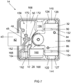
- FIG. 7 is the lamp base 14 according to the embodiment in a bottom view without socket cover with the board 50, the base member 32 and the socket 42 shown.
- the base member 32 is welded to the board 50 via the cantilevered contact portions 127, 128 of the contact plates 122, 124 with resistance spot welding, or alternatively laser welding.
- the welding areas 144, 146 required for this purpose lie between the contacting side 82 of the base element 32 FIG. 6 By the welding, the base member 32 is mechanically connected to the circuit board 50 on the one hand, and on the other hand, the primary winding 88 of the transformer 54 from FIG. 3 electrically contacted with the board 50.
- the circuit board 50 has expansion joints 152, 154 in the region of the contact pins 90, 92 of the base element 32. These extend substantially finger-like vertically from one in the FIG. 7 For example, changes in volume of the circuit board 50 due to temperature fluctuations in the operation of the high-pressure discharge lamp 1 from the expansion joints 152, 154 from the right board side 156 approximately in the area below the base element FIG. 1 or expansions of the Silikonvergusses of the base member 32, which are transmitted for example via the welded contact portions 127, 128 on the board 50, are compensated.
- Another function of the expansion joints 152, 154 is that they can accommodate the contact pins 90, 92, if they are from the contacting side 82 of the base member 32, see FIG. 6 , cantilever, bringing a roughly planar support opportunity the contacting side 82 on the board 50 is made possible also in this case.
- dowel pins 84, 86 which in the FIG. 7 are arranged approximately in the vicinity of the welding areas 146, 148, with the board 50, a relief of the welding areas 146, 148 of thermal and dynamic forces of change between the base member 32 and the board 50 is made possible.
- FIGS. 7 and 2 It can be seen that an easily accessible from the outside space 158 is essentially delimited by the board 50, by the lateral surface portion 40 of the lamp cap 14, the central dome 28 and the base member 32. About the space 158, the board 50 can be easily equipped with electrical components.
- the electrical components used here are, for example, a capacitor 160, which in the FIG. 7 is mounted approximately below the central dome 28 on the board 50 and how out FIG. 2 Visible about half the height of the base member 32, resistors 162, a suppressor diode 164 and various other electronic components 166.
- the board 50 also offers a significant surface potential to integrate further components, such as a throttle, not shown, which can be arranged between the contacting points 170, 172.
- the return conductor or the power supply 12 of the halogen discharge lamp 1 off FIG. 1 is passed through the contact point 172 as a pin-in-hole connection and is additionally welded to the board 50 via this.
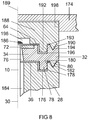
- FIG. 8 shows in a side view a cross section through the middle dome 28, the base member 32 and a base cover 174 according to the embodiment for more accurate representation of the connection between these components.
- the center dome 28 has to receive the annular spring 78 of the center contact ring 34 of the base member 32 has an annular groove 176 on the Domstirn nature 36, which is designed such that the annular spring 78 substantially abuts only with a ring outer surface 178 on a Nutwandungs character 180 and thus the annular spring 78 and the annular groove 176 form a fit.
- the point-shaped energy directors 80 of the center contact ring 34 completely fills a receiving groove 182 which is likewise pointed-shaped on the dome end face 36 of the central dome 28.
- the center contact ring 34 can be welded to the central dome 28 via an ultrasonic welding process.
- ultrasound welding leads to a high high-voltage strength of the connection point and, on the other hand, low geometric manufacturing tolerances can be achieved as a result.
- the load due to the high-frequency ultrasonic vibrations is effective only in the region of the center contact ring 34.
- the silicone potting in the Transformer chamber 52 off FIG. 3 Due to its high inertia, it does not carry the ultrasonic vibrations. Is the discharge vessel 4 off FIG.
- connection between the energy directing device 80 and the receiving groove 182 can also be realized, for example, with an adhesive joint with a 2K epoxy resin, such as DeloDuopox from Delo.
- the middle dome 28 in FIG. 5 has a power supply channel 184 for receiving the power supply 10 of the discharge vessel 4 from FIG. 1 with the power supply channel 184 extending along the base longitudinal axis 30 of the central dome 28 and leading to the funnel 76 of the center contact ring 34.
- the power supply 10 is passed through the power supply channel 184 and the funnel 76 through the through hole 72 of the center contact element 66 and welded by a welding tip 186 with the center contact element 66 and thus electrically contacted and mechanically connected.
- the base cover 174 is in the FIG. 5 only partially shown. This is fixedly connected via a cylindrical cover spacer 188 with the center contact ring 34.
- the cover intermediate piece axis 189 lies approximately on the base longitudinal axis 30 of the central dome 28.
- an energy directors 190 and an annular spring 192 are in a receiving groove 194 and an annular groove 196 which are respectively formed on the ring top 64 of the center contact ring 34 and the receiving groove 182 and the annular groove 176 of the central dome 28 correspond.
- the receiving groove 194 and the annular groove 196 are only in this FIG. 8 shown.
- a receiving region 196 is centered back from the middle of the intermediate piece underside 193, by means of which the welding tip 186 is receivable and thus spaced from the cover intermediate piece 188.
- the welding with the welding tip 186 is isolated by the cover spacer 188 and the socket cover 174 high-voltage resistant.
- the cover spacer 188 is inserted into a cylindrical recess 198 of the base lid 174 and firmly connected to this example by adhesive.
- the socket cover 174 is made of inexpensive plastic such as PA66, and the cover spacer 188 made of PPS corresponding to the socket member 32.
- the assembled board 50 in FIG. 7 is on the pin-in-hole connections of the contact pins 46, 48 of the socket 42 and the power supply 12 of the high pressure discharge lamp 1 from FIG. 1 and the welding areas 144, 146 of the base member 32 fixed.
- a so-called hot caulking for fixing the board, as in the prior art, can be omitted.
- a multi-part lamp cap with a separate base element, wherein in the base element, a transformer is accommodated, in which at least one winding is fixed via a contact pin.
Landscapes
- Engineering & Computer Science (AREA)
- Power Engineering (AREA)
- Fastening Of Light Sources Or Lamp Holders (AREA)
- Arrangement Of Elements, Cooling, Sealing, Or The Like Of Lighting Devices (AREA)
Claims (16)
- Élément de culot de lampe (32) comprenant un transformateur (54) muni d'une chambre de transformateur (52) logeant le transformateur (54), le transformateur (54) étant entièrement logé dans la chambre de transformateur (52) et présentant un boîtier de transformateur (60) qui entoure un noyau de transformateur (56) muni d'un premier enroulement (58), et un deuxième enroulement (88) étant disposé autour du boîtier de transformateur (60),lequel enroulement est fixé sur le boîtier de transformateur (60) à l'aide d'au moins un élément de contact (90, 92), caractérisé en ce que des broches de contact (90, 92) du transformateur (54) sont guidées à travers un côté de mise en contact (82) de la chambre de transformateur (52), opposé à un côté d'ouverture (62).
- Élément de culot de lampe selon la revendication 1, un élément de contact central (66) étant placé dans la chambre de transformateur (52) de manière à ce qu'une zone de contact de transformateur (114) de l'élément de contact central (66), pour la mise en contact du premier enroulement (58) du transformateur (54) guidé hors du boîtier de transformateur (60), soit disposée à l'intérieur de la chambre de transformateur (52) et en ce qu'une zone supplémentaire de contact de lampe (68), notamment pour la mise en contact d'une lampe à décharge (1) à haute pression, soit disposée à l'extérieur de la chambre de transformateur (52).
- Élément de culot de lampe selon la revendication 1 ou 2, une surface d'enveloppe de la chambre de transformateur (52), délimitant le côté d'ouverture (62), présentant deux grands côtés (108) et deux côtés transversaux (112, 138) qui sont essentiellement disposés en angle droit les uns par rapport aux autres.
- Élément de culot de lampe selon la revendication 3, la zone de contact de lampe (68) de l'élément de contact central (66) étant logée dans une bague de contact centrale (34) qui est formée sur le grand côté (108) de manière centrée en direction longitudinale du grand côté (108) de la chambre de transformateur (52) de manière à ce qu'un axe de bague (70) s'étende approximativement parallèlement à une broche de contact (90, 92) du transformateur (54) et qu'un côté supérieur de bague (64) se termine approximativement de manière affleurée avec le côté d'ouverture (62) de la chambre de transformateur (52).
- Élément de culot de lampe selon la revendication 4, un entonnoir (76) étant formé approximativement au centre de la bague de contact centrale (34), lequel se rétrécit le long de l'axe de bague (70) en direction de la normale à la surface du côté d'ouverture (62) de la chambre de transformateur (52) jusqu'à la zone de contact de lampe (68) de l'élément de contact central (66).
- Élément de culot de lampe selon la revendication 4 ou 5, la bague de contact centrale (34) formant sur un côté inférieur de bague (75) un ressort annulaire (78) et un capteur de direction d'énergie (80) annulaire présentant un rayon plus grand que le ressort annulaire (78), ayant une section transversale en forme de pointe respectivement pour la liaison avec le culot de lampe (14).
- Élément de culot de lampe selon l'une quelconque des revendications 1 à 6, les broches de contact (90, 92) étant en liaison avec des plaques de contact (122, 124) depuis l'extérieur sur le côté de mise en contact (82) de la chambre de transformateur (52).
- Élément de culot de lampe selon l'une quelconque des revendications 1 à 7, au moins une goupille d'ajustement (84, 86) étant réalisée sur le côté de mise en contact (82) de l'élément de culot de lampe (32).
- Culot de lampe, notamment pour le logement d'une lampe à décharge (1) à haute pression, comprenant une plaque de support (24), un dôme central (28) cylindrique étant centralement formé sur un côté du support (26) de la plaque de support (24), détourné de la lampe à décharge (1) à haute pression, un élément de culot de lampe (32) selon l'une quelconque ou plusieurs des revendications 1 à 8 étant approximativement adjacent à un côté de tête de dôme central (36) avec le côté inférieur de bague (75) et étant fixé sur le dôme central (28).
- Culot de lampe selon la revendication 9, des broches de contact (46, 48) d'un connecteur (42), intégrées dans le culot de lampe (14), faisant saillie hors du côté du support (26) et ayant prise dans des évidements d'une platine (50) disposée avec écart parallèle à la plaque de support (24), le dôme central (28) cylindrique s'étendant en traversant un évidement de la platine (50).
- Culot de lampe selon l'une quelconque des revendications 9 ou 10, le ressort annulaire (78) et le capteur de direction d'énergie (80) de l'élément de culot de lampe (32) plongeant dans respectivement une rainure annulaire (176) et un logement annulaire (178) du dôme central (28).
- Culot de lampe selon l'une quelconque des revendications 9 à 11, le dôme central (28) présentant un canal d'alimentation en courant (184) logeant une alimentation en courant (10), lequel s'étend le long de l'axe médian (30) du dôme central (28) et débouche vers l'entonnoir (76) de l'élément de culot de lampe (32).
- Culot de lampe selon l'une quelconque des revendications 9 à 12, un couvercle de culot (174) entourant le culot de lampe (14), le couvercle de culot (174) formant un ressort annulaire (192) pour la liaison mécanique avec le culot de lampe (14) et un capteur de direction d'énergie (190) annulaire, lesquels sont respectivement immergés dans une rainure annulaire (196) et dans un logement annulaire (194) de l'élément de culot de lampe (32).
- Culot de lampe selon l'une quelconque des revendications 10 à 13, la platine (50) présentant des joints de dilatation (152, 154) dans la zone des broches de contact (90, 92) de l'élément de culot de lampe (32).
- Culot de lampe selon l'une quelconque des revendications 9 à 14, l'au moins une goupille d'ajustement (84, 86) de l'élément de culot de lampe (32) étant immergée dans au moins un logement de broche de la platine (50).
- Lampe à décharge comprenant un culot de lampe (14) selon l'une quelconque ou plusieurs des revendications 9 à 15.
Applications Claiming Priority (2)
| Application Number | Priority Date | Filing Date | Title |
|---|---|---|---|
| DE102008033192A DE102008033192A1 (de) | 2008-07-15 | 2008-07-15 | Transformator sowie Lampensockelelement, Lampensockel und Entladungslampe mit einem derartigen Lampensockel |
| PCT/EP2009/057952 WO2010006911A1 (fr) | 2008-07-15 | 2009-06-25 | Transformateur ainsi qu’élément de culot de lampe, culot de lampe et lampe à décharge avec un culot de lampe de ce type |
Publications (2)
| Publication Number | Publication Date |
|---|---|
| EP2297752A1 EP2297752A1 (fr) | 2011-03-23 |
| EP2297752B1 true EP2297752B1 (fr) | 2017-09-20 |
Family
ID=41110638
Family Applications (1)
| Application Number | Title | Priority Date | Filing Date |
|---|---|---|---|
| EP09779942.3A Not-in-force EP2297752B1 (fr) | 2008-07-15 | 2009-06-25 | Transformateur ainsi que élément de culot de lampe, culot de lampe et lampe à décharge avec un culot de lampe de ce type |
Country Status (6)
| Country | Link |
|---|---|
| US (1) | US8742663B2 (fr) |
| EP (1) | EP2297752B1 (fr) |
| JP (1) | JP5595394B2 (fr) |
| CN (1) | CN102099879B (fr) |
| DE (1) | DE102008033192A1 (fr) |
| WO (1) | WO2010006911A1 (fr) |
Families Citing this family (5)
| Publication number | Priority date | Publication date | Assignee | Title |
|---|---|---|---|---|
| DE102010041595A1 (de) * | 2010-09-29 | 2012-03-29 | Siemens Aktiengesellschaft | Anordnung und Verfahren zum elektrischen Kontaktieren von elektrischen Leitern in Spulen |
| US9343286B2 (en) | 2012-04-27 | 2016-05-17 | Koninklijke Philips N.V. | Lamp with electrical components embedded in an insulation compound |
| ES2667098T3 (es) | 2014-08-04 | 2018-05-09 | Flowil International Lighting (Holding) B.V. | Lámpara de reemplazo y de ahorro de energía con bobina magnética integrada y con quemador de halogenuros metálicos cerámicos para sustituir lámparas de vapor de mercurio, lámparas de sodio de alta presión y lámparas de halogenuros metálicos de cuarzo |
| DE202018105238U1 (de) * | 2018-09-13 | 2019-12-16 | Zumtobel Lighting Gmbh | Leuchte |
| DE102020212993A1 (de) | 2020-10-15 | 2022-04-21 | Siemens Energy Global GmbH & Co. KG | Verfahren zur Verringerung einer von einem Eisenkern eines Transformators ausgehenden Geräuschbelastung, Eisenkern sowie Transformator |
Family Cites Families (17)
| Publication number | Priority date | Publication date | Assignee | Title |
|---|---|---|---|---|
| JPH08130127A (ja) * | 1994-06-15 | 1996-05-21 | Nippondenso Co Ltd | 高圧トランス及び放電灯回路 |
| JPH10214736A (ja) | 1997-01-28 | 1998-08-11 | Toyo Denso Co Ltd | 高電圧発生用トランス |
| JP3670144B2 (ja) | 1998-10-15 | 2005-07-13 | 三菱電機株式会社 | 放電灯点灯装置 |
| JP3090448B1 (ja) | 1999-09-30 | 2000-09-18 | 松下電工株式会社 | ランプソケット及び放電灯点灯装置 |
| WO2004066686A1 (fr) | 2003-01-22 | 2004-08-05 | Philips Intellectual Property & Standards Gmbh | Ensemble lampe a decharge a raccordement stable entre le culot de lampe et le logement du demarreur |
| DE20312503U1 (de) * | 2003-08-11 | 2003-12-24 | Niggemeyer, Gert Günther, Ing.(grad.) | Stabförmiger Zündübertrager |
| DE10339588A1 (de) | 2003-08-26 | 2005-03-24 | Patent-Treuhand-Gesellschaft für elektrische Glühlampen mbH | Lampensockel für eine Hochdruckentladungslampe und Hochdruckentladungslampe |
| DE10339587A1 (de) * | 2003-08-26 | 2005-03-24 | Patent-Treuhand-Gesellschaft für elektrische Glühlampen mbH | Transformator, Lampensockel mit einem Transformator und Hochdruckentladungslampe |
| DE10339594A1 (de) * | 2003-08-26 | 2005-03-24 | Patent-Treuhand-Gesellschaft für elektrische Glühlampen mbH | Lampensockel für eine Hochdruckentladungslampe und Hochdruckentladungslampe |
| JP4281597B2 (ja) | 2004-03-26 | 2009-06-17 | パナソニック電工株式会社 | 放電灯始動装置および放電灯点灯装置および車両用前照灯器具および車両 |
| DE102004044368A1 (de) * | 2004-09-10 | 2006-03-16 | Patent-Treuhand-Gesellschaft für elektrische Glühlampen mbH | Transformator und Zündvorrichtung mit einem Transformator sowie Hochdruckentladungslampe mit einem Transformator |
| DE102005029001A1 (de) * | 2005-02-11 | 2006-08-24 | Patent-Treuhand-Gesellschaft für elektrische Glühlampen mbH | Lampensockel für eine Hochdruckentladungslampe und Hochdrucksentladungslampe |
| JP4426995B2 (ja) * | 2005-03-28 | 2010-03-03 | パナソニック電工株式会社 | 高電圧パルス発生器、及びそれを用いた照明器具、並びに車両 |
| DE102005023797A1 (de) * | 2005-05-19 | 2006-11-23 | Patent-Treuhand-Gesellschaft für elektrische Glühlampen mbH | Sockel für eine Lampe |
| JP2007134098A (ja) | 2005-11-09 | 2007-05-31 | Harison Toshiba Lighting Corp | 放電ランプ装置および放電ランプ装置の製造方法 |
| DE102006014695A1 (de) | 2006-03-28 | 2007-10-04 | Patent-Treuhand-Gesellschaft für elektrische Glühlampen mbH | Verfahren zur Herstellung eines elektrisch isolierenden Vergusskörpers und ein Sockel für eine Lampe |
| US7855625B2 (en) * | 2006-08-31 | 2010-12-21 | General Electric Company | Lamp transformer |
-
2008
- 2008-07-15 DE DE102008033192A patent/DE102008033192A1/de not_active Withdrawn
-
2009
- 2009-06-25 EP EP09779942.3A patent/EP2297752B1/fr not_active Not-in-force
- 2009-06-25 US US13/003,878 patent/US8742663B2/en not_active Expired - Fee Related
- 2009-06-25 CN CN2009801279601A patent/CN102099879B/zh not_active Expired - Fee Related
- 2009-06-25 WO PCT/EP2009/057952 patent/WO2010006911A1/fr active Application Filing
- 2009-06-25 JP JP2011517845A patent/JP5595394B2/ja not_active Expired - Fee Related
Non-Patent Citations (1)
| Title |
|---|
| None * |
Also Published As
| Publication number | Publication date |
|---|---|
| CN102099879B (zh) | 2013-07-10 |
| DE102008033192A1 (de) | 2010-01-21 |
| WO2010006911A1 (fr) | 2010-01-21 |
| JP2011528179A (ja) | 2011-11-10 |
| US8742663B2 (en) | 2014-06-03 |
| EP2297752A1 (fr) | 2011-03-23 |
| US20110115374A1 (en) | 2011-05-19 |
| JP5595394B2 (ja) | 2014-09-24 |
| CN102099879A (zh) | 2011-06-15 |
Similar Documents
| Publication | Publication Date | Title |
|---|---|---|
| EP1727261B2 (fr) | Stator pour moteur électrique | |
| EP1718937B1 (fr) | Support de capteur et procede de realisation associe | |
| DE102011013449B4 (de) | Baugruppe mit einem Träger, einem SMD-Bauteil und einem Stanzgitterteil | |
| EP2567426B1 (fr) | Connexion de module électrique d'un véhicule à moteur | |
| EP2567429B1 (fr) | Connexion de module électrique d'un véhicule à moteur | |
| EP2297752B1 (fr) | Transformateur ainsi que élément de culot de lampe, culot de lampe et lampe à décharge avec un culot de lampe de ce type | |
| WO2007131374A1 (fr) | Interrupteur de proximité et procédé de mise en contact d'une carte à circuit imprimé de capteur | |
| EP2057406A1 (fr) | Lampe comprenant un socle et au moins un composant a semi-conducteur luminescent | |
| US11521818B2 (en) | Fuses and methods of forming fuses | |
| DE10008572B4 (de) | Verbindungseinrichtung für Leistungshalbleitermodule | |
| EP3109951B1 (fr) | Composant electrique, unite de connexion comprenant au moins un composant electrique, vehicule ainsi equipe et procede de fabrication d'un composant electrique | |
| DE4327309C2 (de) | Zündvorrichtung für einen Verbrennungsmotor | |
| EP2018520A2 (fr) | Boîtier de capteur | |
| WO1997007540A1 (fr) | Boitier pour composants et modules micro-electroniques et son procede de production | |
| DE102010039740A1 (de) | Kontaktelement zur Kontaktierung eines Schaltungsträgers, sowie Schaltungsträger mit einem Kontaktelement | |
| EP1518283A2 (fr) | Pole de raccordement d'un accumulateur | |
| DE19804669A1 (de) | Elektrisches Kontaktelement | |
| EP0930635B1 (fr) | Lampe à décharge haute pression à culot unique | |
| DE4108416C2 (de) | Kraftstoff-Einspritzdüse für Brennkraftmaschinen | |
| EP0728986A1 (fr) | Douille pour connecter une lampe à décharge à gaz | |
| WO2013000753A2 (fr) | Prise de courant pour modules photovoltaïques | |
| DE10129840B4 (de) | Elektrisches Gerät | |
| EP2269268B1 (fr) | Contact pour courant fort, et composant électrique présentant un contact pour courant fort | |
| DE10228445A1 (de) | Fahrzeugleuchte | |
| WO2015028254A1 (fr) | Nouveau type de connexion d'un circuit imprimé souple au boîtier d'un appareil de commande |
Legal Events
| Date | Code | Title | Description |
|---|---|---|---|
| PUAI | Public reference made under article 153(3) epc to a published international application that has entered the european phase |
Free format text: ORIGINAL CODE: 0009012 |
|
| 17P | Request for examination filed |
Effective date: 20101130 |
|
| AK | Designated contracting states |
Kind code of ref document: A1 Designated state(s): AT BE BG CH CY CZ DE DK EE ES FI FR GB GR HR HU IE IS IT LI LT LU LV MC MK MT NL NO PL PT RO SE SI SK TR |
|
| AX | Request for extension of the european patent |
Extension state: AL BA RS |
|
| DAX | Request for extension of the european patent (deleted) | ||
| RAP1 | Party data changed (applicant data changed or rights of an application transferred) |
Owner name: OSRAM AG |
|
| RAP1 | Party data changed (applicant data changed or rights of an application transferred) |
Owner name: OSRAM GMBH |
|
| RAP1 | Party data changed (applicant data changed or rights of an application transferred) |
Owner name: OSRAM GMBH |
|
| 17Q | First examination report despatched |
Effective date: 20161221 |
|
| GRAP | Despatch of communication of intention to grant a patent |
Free format text: ORIGINAL CODE: EPIDOSNIGR1 |
|
| INTG | Intention to grant announced |
Effective date: 20170519 |
|
| GRAS | Grant fee paid |
Free format text: ORIGINAL CODE: EPIDOSNIGR3 |
|
| GRAA | (expected) grant |
Free format text: ORIGINAL CODE: 0009210 |
|
| AK | Designated contracting states |
Kind code of ref document: B1 Designated state(s): AT BE BG CH CY CZ DE DK EE ES FI FR GB GR HR HU IE IS IT LI LT LU LV MC MK MT NL NO PL PT RO SE SI SK TR |
|
| REG | Reference to a national code |
Ref country code: GB Ref legal event code: FG4D Free format text: NOT ENGLISH |
|
| REG | Reference to a national code |
Ref country code: CH Ref legal event code: EP |
|
| REG | Reference to a national code |
Ref country code: AT Ref legal event code: REF Ref document number: 930763 Country of ref document: AT Kind code of ref document: T Effective date: 20171015 |
|
| REG | Reference to a national code |
Ref country code: IE Ref legal event code: FG4D Free format text: LANGUAGE OF EP DOCUMENT: GERMAN |
|
| REG | Reference to a national code |
Ref country code: DE Ref legal event code: R096 Ref document number: 502009014391 Country of ref document: DE |
|
| REG | Reference to a national code |
Ref country code: NL Ref legal event code: MP Effective date: 20170920 |
|
| PG25 | Lapsed in a contracting state [announced via postgrant information from national office to epo] |
Ref country code: NO Free format text: LAPSE BECAUSE OF FAILURE TO SUBMIT A TRANSLATION OF THE DESCRIPTION OR TO PAY THE FEE WITHIN THE PRESCRIBED TIME-LIMIT Effective date: 20171220 Ref country code: LT Free format text: LAPSE BECAUSE OF FAILURE TO SUBMIT A TRANSLATION OF THE DESCRIPTION OR TO PAY THE FEE WITHIN THE PRESCRIBED TIME-LIMIT Effective date: 20170920 Ref country code: FI Free format text: LAPSE BECAUSE OF FAILURE TO SUBMIT A TRANSLATION OF THE DESCRIPTION OR TO PAY THE FEE WITHIN THE PRESCRIBED TIME-LIMIT Effective date: 20170920 Ref country code: HR Free format text: LAPSE BECAUSE OF FAILURE TO SUBMIT A TRANSLATION OF THE DESCRIPTION OR TO PAY THE FEE WITHIN THE PRESCRIBED TIME-LIMIT Effective date: 20170920 Ref country code: SE Free format text: LAPSE BECAUSE OF FAILURE TO SUBMIT A TRANSLATION OF THE DESCRIPTION OR TO PAY THE FEE WITHIN THE PRESCRIBED TIME-LIMIT Effective date: 20170920 |
|
| REG | Reference to a national code |
Ref country code: LT Ref legal event code: MG4D |
|
| PG25 | Lapsed in a contracting state [announced via postgrant information from national office to epo] |
Ref country code: BG Free format text: LAPSE BECAUSE OF FAILURE TO SUBMIT A TRANSLATION OF THE DESCRIPTION OR TO PAY THE FEE WITHIN THE PRESCRIBED TIME-LIMIT Effective date: 20171220 Ref country code: LV Free format text: LAPSE BECAUSE OF FAILURE TO SUBMIT A TRANSLATION OF THE DESCRIPTION OR TO PAY THE FEE WITHIN THE PRESCRIBED TIME-LIMIT Effective date: 20170920 Ref country code: GR Free format text: LAPSE BECAUSE OF FAILURE TO SUBMIT A TRANSLATION OF THE DESCRIPTION OR TO PAY THE FEE WITHIN THE PRESCRIBED TIME-LIMIT Effective date: 20171221 |
|
| PG25 | Lapsed in a contracting state [announced via postgrant information from national office to epo] |
Ref country code: NL Free format text: LAPSE BECAUSE OF FAILURE TO SUBMIT A TRANSLATION OF THE DESCRIPTION OR TO PAY THE FEE WITHIN THE PRESCRIBED TIME-LIMIT Effective date: 20170920 |
|
| PG25 | Lapsed in a contracting state [announced via postgrant information from national office to epo] |
Ref country code: ES Free format text: LAPSE BECAUSE OF FAILURE TO SUBMIT A TRANSLATION OF THE DESCRIPTION OR TO PAY THE FEE WITHIN THE PRESCRIBED TIME-LIMIT Effective date: 20170920 Ref country code: PL Free format text: LAPSE BECAUSE OF FAILURE TO SUBMIT A TRANSLATION OF THE DESCRIPTION OR TO PAY THE FEE WITHIN THE PRESCRIBED TIME-LIMIT Effective date: 20170920 Ref country code: RO Free format text: LAPSE BECAUSE OF FAILURE TO SUBMIT A TRANSLATION OF THE DESCRIPTION OR TO PAY THE FEE WITHIN THE PRESCRIBED TIME-LIMIT Effective date: 20170920 Ref country code: CZ Free format text: LAPSE BECAUSE OF FAILURE TO SUBMIT A TRANSLATION OF THE DESCRIPTION OR TO PAY THE FEE WITHIN THE PRESCRIBED TIME-LIMIT Effective date: 20170920 |
|
| PG25 | Lapsed in a contracting state [announced via postgrant information from national office to epo] |
Ref country code: EE Free format text: LAPSE BECAUSE OF FAILURE TO SUBMIT A TRANSLATION OF THE DESCRIPTION OR TO PAY THE FEE WITHIN THE PRESCRIBED TIME-LIMIT Effective date: 20170920 Ref country code: IS Free format text: LAPSE BECAUSE OF FAILURE TO SUBMIT A TRANSLATION OF THE DESCRIPTION OR TO PAY THE FEE WITHIN THE PRESCRIBED TIME-LIMIT Effective date: 20180120 Ref country code: SK Free format text: LAPSE BECAUSE OF FAILURE TO SUBMIT A TRANSLATION OF THE DESCRIPTION OR TO PAY THE FEE WITHIN THE PRESCRIBED TIME-LIMIT Effective date: 20170920 Ref country code: IT Free format text: LAPSE BECAUSE OF FAILURE TO SUBMIT A TRANSLATION OF THE DESCRIPTION OR TO PAY THE FEE WITHIN THE PRESCRIBED TIME-LIMIT Effective date: 20170920 |
|
| REG | Reference to a national code |
Ref country code: FR Ref legal event code: PLFP Year of fee payment: 10 |
|
| REG | Reference to a national code |
Ref country code: DE Ref legal event code: R097 Ref document number: 502009014391 Country of ref document: DE |
|
| PLBE | No opposition filed within time limit |
Free format text: ORIGINAL CODE: 0009261 |
|
| STAA | Information on the status of an ep patent application or granted ep patent |
Free format text: STATUS: NO OPPOSITION FILED WITHIN TIME LIMIT |
|
| PG25 | Lapsed in a contracting state [announced via postgrant information from national office to epo] |
Ref country code: DK Free format text: LAPSE BECAUSE OF FAILURE TO SUBMIT A TRANSLATION OF THE DESCRIPTION OR TO PAY THE FEE WITHIN THE PRESCRIBED TIME-LIMIT Effective date: 20170920 |
|
| PGFP | Annual fee paid to national office [announced via postgrant information from national office to epo] |
Ref country code: DE Payment date: 20180625 Year of fee payment: 10 |
|
| 26N | No opposition filed |
Effective date: 20180621 |
|
| PGFP | Annual fee paid to national office [announced via postgrant information from national office to epo] |
Ref country code: FR Payment date: 20180620 Year of fee payment: 10 |
|
| PG25 | Lapsed in a contracting state [announced via postgrant information from national office to epo] |
Ref country code: MT Free format text: LAPSE BECAUSE OF FAILURE TO SUBMIT A TRANSLATION OF THE DESCRIPTION OR TO PAY THE FEE WITHIN THE PRESCRIBED TIME-LIMIT Effective date: 20170920 |
|
| PG25 | Lapsed in a contracting state [announced via postgrant information from national office to epo] |
Ref country code: SI Free format text: LAPSE BECAUSE OF FAILURE TO SUBMIT A TRANSLATION OF THE DESCRIPTION OR TO PAY THE FEE WITHIN THE PRESCRIBED TIME-LIMIT Effective date: 20170920 |
|
| REG | Reference to a national code |
Ref country code: CH Ref legal event code: PL |
|
| GBPC | Gb: european patent ceased through non-payment of renewal fee |
Effective date: 20180625 |
|
| REG | Reference to a national code |
Ref country code: BE Ref legal event code: MM Effective date: 20180630 |
|
| REG | Reference to a national code |
Ref country code: IE Ref legal event code: MM4A |
|
| PG25 | Lapsed in a contracting state [announced via postgrant information from national office to epo] |
Ref country code: MC Free format text: LAPSE BECAUSE OF FAILURE TO SUBMIT A TRANSLATION OF THE DESCRIPTION OR TO PAY THE FEE WITHIN THE PRESCRIBED TIME-LIMIT Effective date: 20170920 Ref country code: LU Free format text: LAPSE BECAUSE OF NON-PAYMENT OF DUE FEES Effective date: 20180625 |
|
| PG25 | Lapsed in a contracting state [announced via postgrant information from national office to epo] |
Ref country code: CH Free format text: LAPSE BECAUSE OF NON-PAYMENT OF DUE FEES Effective date: 20180630 Ref country code: GB Free format text: LAPSE BECAUSE OF NON-PAYMENT OF DUE FEES Effective date: 20180625 Ref country code: IE Free format text: LAPSE BECAUSE OF NON-PAYMENT OF DUE FEES Effective date: 20180625 Ref country code: LI Free format text: LAPSE BECAUSE OF NON-PAYMENT OF DUE FEES Effective date: 20180630 |
|
| PG25 | Lapsed in a contracting state [announced via postgrant information from national office to epo] |
Ref country code: BE Free format text: LAPSE BECAUSE OF NON-PAYMENT OF DUE FEES Effective date: 20180630 |
|
| REG | Reference to a national code |
Ref country code: AT Ref legal event code: MM01 Ref document number: 930763 Country of ref document: AT Kind code of ref document: T Effective date: 20180625 |
|
| PG25 | Lapsed in a contracting state [announced via postgrant information from national office to epo] |
Ref country code: AT Free format text: LAPSE BECAUSE OF NON-PAYMENT OF DUE FEES Effective date: 20180625 |
|
| REG | Reference to a national code |
Ref country code: DE Ref legal event code: R119 Ref document number: 502009014391 Country of ref document: DE |
|
| PG25 | Lapsed in a contracting state [announced via postgrant information from national office to epo] |
Ref country code: TR Free format text: LAPSE BECAUSE OF FAILURE TO SUBMIT A TRANSLATION OF THE DESCRIPTION OR TO PAY THE FEE WITHIN THE PRESCRIBED TIME-LIMIT Effective date: 20170920 |
|
| PG25 | Lapsed in a contracting state [announced via postgrant information from national office to epo] |
Ref country code: DE Free format text: LAPSE BECAUSE OF NON-PAYMENT OF DUE FEES Effective date: 20200101 |
|
| PG25 | Lapsed in a contracting state [announced via postgrant information from national office to epo] |
Ref country code: HU Free format text: LAPSE BECAUSE OF FAILURE TO SUBMIT A TRANSLATION OF THE DESCRIPTION OR TO PAY THE FEE WITHIN THE PRESCRIBED TIME-LIMIT; INVALID AB INITIO Effective date: 20090625 Ref country code: PT Free format text: LAPSE BECAUSE OF FAILURE TO SUBMIT A TRANSLATION OF THE DESCRIPTION OR TO PAY THE FEE WITHIN THE PRESCRIBED TIME-LIMIT Effective date: 20170920 |
|
| PG25 | Lapsed in a contracting state [announced via postgrant information from national office to epo] |
Ref country code: FR Free format text: LAPSE BECAUSE OF NON-PAYMENT OF DUE FEES Effective date: 20190630 Ref country code: CY Free format text: LAPSE BECAUSE OF FAILURE TO SUBMIT A TRANSLATION OF THE DESCRIPTION OR TO PAY THE FEE WITHIN THE PRESCRIBED TIME-LIMIT Effective date: 20170920 Ref country code: MK Free format text: LAPSE BECAUSE OF NON-PAYMENT OF DUE FEES Effective date: 20170920 |