EP2297619B1 - Système de surveillance - Google Patents
Système de surveillance Download PDFInfo
- Publication number
- EP2297619B1 EP2297619B1 EP09768971.5A EP09768971A EP2297619B1 EP 2297619 B1 EP2297619 B1 EP 2297619B1 EP 09768971 A EP09768971 A EP 09768971A EP 2297619 B1 EP2297619 B1 EP 2297619B1
- Authority
- EP
- European Patent Office
- Prior art keywords
- output
- signal
- control signal
- module
- crack
- Prior art date
- Legal status (The legal status is an assumption and is not a legal conclusion. Google has not performed a legal analysis and makes no representation as to the accuracy of the status listed.)
- Active
Links
- 238000012544 monitoring process Methods 0.000 title claims description 70
- 238000000034 method Methods 0.000 claims description 25
- 230000004044 response Effects 0.000 claims description 12
- 238000004891 communication Methods 0.000 claims description 6
- 238000012546 transfer Methods 0.000 claims description 4
- OWZREIFADZCYQD-NSHGMRRFSA-N deltamethrin Chemical compound CC1(C)[C@@H](C=C(Br)Br)[C@H]1C(=O)O[C@H](C#N)C1=CC=CC(OC=2C=CC=CC=2)=C1 OWZREIFADZCYQD-NSHGMRRFSA-N 0.000 claims 14
- 230000002401 inhibitory effect Effects 0.000 claims 2
- 230000035515 penetration Effects 0.000 description 24
- 230000008569 process Effects 0.000 description 19
- 230000005540 biological transmission Effects 0.000 description 17
- 238000012545 processing Methods 0.000 description 13
- 230000008878 coupling Effects 0.000 description 5
- 238000010168 coupling process Methods 0.000 description 5
- 238000005859 coupling reaction Methods 0.000 description 5
- 238000010586 diagram Methods 0.000 description 5
- 239000003990 capacitor Substances 0.000 description 4
- 239000000872 buffer Substances 0.000 description 3
- 238000012806 monitoring device Methods 0.000 description 3
- 230000007246 mechanism Effects 0.000 description 2
- 238000012360 testing method Methods 0.000 description 2
- 230000001960 triggered effect Effects 0.000 description 2
- 230000002457 bidirectional effect Effects 0.000 description 1
- 230000000903 blocking effect Effects 0.000 description 1
- 125000004122 cyclic group Chemical group 0.000 description 1
- 230000006378 damage Effects 0.000 description 1
- 238000013524 data verification Methods 0.000 description 1
- 230000007423 decrease Effects 0.000 description 1
- 238000013461 design Methods 0.000 description 1
- 238000003780 insertion Methods 0.000 description 1
- 230000037431 insertion Effects 0.000 description 1
- 238000002955 isolation Methods 0.000 description 1
- 238000004519 manufacturing process Methods 0.000 description 1
- 230000002035 prolonged effect Effects 0.000 description 1
- 230000001681 protective effect Effects 0.000 description 1
- 238000012797 qualification Methods 0.000 description 1
- 238000012549 training Methods 0.000 description 1
Images


Classifications
-
- G—PHYSICS
- G05—CONTROLLING; REGULATING
- G05B—CONTROL OR REGULATING SYSTEMS IN GENERAL; FUNCTIONAL ELEMENTS OF SUCH SYSTEMS; MONITORING OR TESTING ARRANGEMENTS FOR SUCH SYSTEMS OR ELEMENTS
- G05B9/00—Safety arrangements
- G05B9/02—Safety arrangements electric
-
- H—ELECTRICITY
- H03—ELECTRONIC CIRCUITRY
- H03K—PULSE TECHNIQUE
- H03K17/00—Electronic switching or gating, i.e. not by contact-making and –breaking
-
- G—PHYSICS
- G05—CONTROLLING; REGULATING
- G05B—CONTROL OR REGULATING SYSTEMS IN GENERAL; FUNCTIONAL ELEMENTS OF SUCH SYSTEMS; MONITORING OR TESTING ARRANGEMENTS FOR SUCH SYSTEMS OR ELEMENTS
- G05B19/00—Programme-control systems
- G05B19/02—Programme-control systems electric
- G05B19/04—Programme control other than numerical control, i.e. in sequence controllers or logic controllers
- G05B19/042—Programme control other than numerical control, i.e. in sequence controllers or logic controllers using digital processors
- G05B19/0428—Safety, monitoring
-
- G—PHYSICS
- G05—CONTROLLING; REGULATING
- G05B—CONTROL OR REGULATING SYSTEMS IN GENERAL; FUNCTIONAL ELEMENTS OF SUCH SYSTEMS; MONITORING OR TESTING ARRANGEMENTS FOR SUCH SYSTEMS OR ELEMENTS
- G05B19/00—Programme-control systems
- G05B19/02—Programme-control systems electric
- G05B19/04—Programme control other than numerical control, i.e. in sequence controllers or logic controllers
- G05B19/048—Monitoring; Safety
-
- G—PHYSICS
- G06—COMPUTING; CALCULATING OR COUNTING
- G06F—ELECTRIC DIGITAL DATA PROCESSING
- G06F11/00—Error detection; Error correction; Monitoring
- G06F11/30—Monitoring
-
- G—PHYSICS
- G05—CONTROLLING; REGULATING
- G05B—CONTROL OR REGULATING SYSTEMS IN GENERAL; FUNCTIONAL ELEMENTS OF SUCH SYSTEMS; MONITORING OR TESTING ARRANGEMENTS FOR SUCH SYSTEMS OR ELEMENTS
- G05B2219/00—Program-control systems
- G05B2219/20—Pc systems
- G05B2219/24—Pc safety
- G05B2219/24021—Separate processor for monitoring system
-
- G—PHYSICS
- G05—CONTROLLING; REGULATING
- G05B—CONTROL OR REGULATING SYSTEMS IN GENERAL; FUNCTIONAL ELEMENTS OF SUCH SYSTEMS; MONITORING OR TESTING ARRANGEMENTS FOR SUCH SYSTEMS OR ELEMENTS
- G05B2219/00—Program-control systems
- G05B2219/20—Pc systems
- G05B2219/24—Pc safety
- G05B2219/24127—Disable, inhibit control signal in I-O interface if alarm status set
-
- G—PHYSICS
- G05—CONTROLLING; REGULATING
- G05B—CONTROL OR REGULATING SYSTEMS IN GENERAL; FUNCTIONAL ELEMENTS OF SUCH SYSTEMS; MONITORING OR TESTING ARRANGEMENTS FOR SUCH SYSTEMS OR ELEMENTS
- G05B2219/00—Program-control systems
- G05B2219/20—Pc systems
- G05B2219/24—Pc safety
- G05B2219/24191—Redundant processors are different in structure
-
- G—PHYSICS
- G05—CONTROLLING; REGULATING
- G05B—CONTROL OR REGULATING SYSTEMS IN GENERAL; FUNCTIONAL ELEMENTS OF SUCH SYSTEMS; MONITORING OR TESTING ARRANGEMENTS FOR SUCH SYSTEMS OR ELEMENTS
- G05B2219/00—Program-control systems
- G05B2219/20—Pc systems
- G05B2219/25—Pc structure of the system
- G05B2219/25428—Field device
-
- G—PHYSICS
- G06—COMPUTING; CALCULATING OR COUNTING
- G06F—ELECTRIC DIGITAL DATA PROCESSING
- G06F17/00—Digital computing or data processing equipment or methods, specially adapted for specific functions
- G06F17/40—Data acquisition and logging
-
- G—PHYSICS
- G16—INFORMATION AND COMMUNICATION TECHNOLOGY [ICT] SPECIALLY ADAPTED FOR SPECIFIC APPLICATION FIELDS
- G16Z—INFORMATION AND COMMUNICATION TECHNOLOGY [ICT] SPECIALLY ADAPTED FOR SPECIFIC APPLICATION FIELDS, NOT OTHERWISE PROVIDED FOR
- G16Z99/00—Subject matter not provided for in other main groups of this subclass
Definitions
- the invention relates to a monitoring system for monitoring safety-relevant processes.
- the document EP 1 128 241 A2 discloses a method and an apparatus for safety monitoring of a control device.
- WO 2008/037495 A2 describes a bus system with a bus to which at least one master, one output slave and one safety monitor are connected, the output slave controlling an output switch and the safety monitor controlling a main switch.
- the document DE 10 2006 001 805 A1 discloses a safety device for multi-channel control of a safety-related device.
- the document US 6,243,629 B1 discloses an electrical control unit for a motor vehicle with a microprocessor, an external sensor connected thereto, an actuator and a monitoring device.
- the microprocessor processes information from the external sensor on the basis of a program stored in the microprocessor and receives test data for checking the operation of the microprocessor from the monitoring device.
- the monitoring device uses the test data to determine solutions that match the processed data sent by the microprocessor. If they do not match, an OR circuit is instructed, a Activate the fail-safe relay, which cuts off the power supply to a solenoid valve.
- An industrial communication system used in data transmission systems which connects a large number of connected field devices, such as measuring sensors (sensors), actuators and / or drives (actuators) with a control device, is known to be a field bus, the devices which provide the actual connection to the bus , are referred to as bus participants.
- the deterministics i.e. the predetermination and immutability in the transmission of process data
- the deterministics are more important than the actual transmission speed itself and receiving process data, such as in particular process input data, process output data and control data
- a cyclical transmission of process data is carried out via a common transmission channel.
- protocol-specific data are often read out from field devices connected to slave participants during predetermined data cycles by a participant acting as a master and written into field devices connected to slave participants during subsequent data cycles.
- the data to be transmitted are also at least partially security-relevant data, so that errors in data transmission must be recognized as early as possible and when an error is recognized reacts promptly, e.g. a field device, a participant or a (sub) system has to be brought into a safe state.
- a field device e.g. a field device
- a participant or a (sub) system e.g. a field device
- a participant or a (sub) system e.g. a participant or a (sub) system has to be brought into a safe state.
- the invention is based on the knowledge that the processing functions of an output module, which controls an actuator containing risk potential, can be implemented in one channel and can also be monitored by a separate monitoring module, for example by a safety master module. If the monitoring module detects a deviation from the expected behavior or an irregularity in the processing sequence, it can transfer the entire system, which can also consist of several output modules, for example several safety output modules, to a safe state. The transfer of the output module (s) to the safe state is implemented independently of the respective processing unit by an auxiliary channel which enables the monitoring module to penetrate and is therefore referred to below as a penetration device.
- the safety function is thus distributed to the monitoring module (safety master) and to the output module (safety output module).
- the safety master is supported by the simple and inexpensive switch-off mechanism of the access device. It is also advantageous for the functioning of the inventive concept to integrate the output enable pulse into the bus protocol, for example.
- By using a decentralized With the microprocessor it is also possible to integrate the control information for the monoflop, which activates or deactivates an output of the output module or a suitable output device.
- the control information can, for example, be modulated into the data signal at fixed times, which enables efficient control of the penetration device.
- the invention relates to a monitoring system with an output module designed to generate a control signal in response to an input signal, a monitoring module designed to generate the input signal for the output module, an output device designed to output an output signal in response to the control signal and a penetration device for preventing or Preventing the output of the output signal, the monitoring module being designed to compare the control signal with a control signal to be expected on the basis of the input signal in order to examine the control signal for the presence of a deviation.
- the monitoring module and the output module are separate modules.
- the output module is designed to transmit the control signal to the monitoring module, and the monitoring module is designed to receive the control signal.
- the monitoring module is further designed, if there is a discrepancy between the control signal and the expected control signal, to instruct the penetration device to prevent or prevent the output of the output signal, the penetration device interrupting a control or data path of the output device to prevent the outputting of the output signal is trained.
- the invention further provides that the monitoring module is designed to generate a release signal and to send it to the output module if the control signal corresponds to the expected control signal, the release signal indicating the release of the output signal.
- the monitoring module and the output module or the penetration device are designed to communicate via a communication network, in particular via a communication bus.
- the penetration device is arranged in the monitoring module or in the output module.
- the output device comprises, for example, a relay or an analog output stage with a data path for receiving the control signal and an energy supply path for supplying the output device with electrical energy.
- the analog output stage can, for example, be designed for a range between 4 mA and 20 mA, the output current of which is less than 3 mA in the event of an error.
- the pass-through device comprises a monostable multivibrator, in particular a flip-flop or a monoflop, the output device having a data path and a power supply path, and wherein an output of the flip-flop in particular via an output transistor with the data path or with the energy supply path for acting on the data path or on the energy supply path is coupled in particular in response to a penetration signal that can be applied to an input of the flip-flop.
- the penetration device is designed to convert the output device into a blocking mode in response to a penetration signal.
- the output module comprises a microcontroller which is provided to receive the input signal and to generate the control signal.
- the invention relates to a method for monitoring an output module by a monitoring module, a control signal being generated by the output module in response to an input signal and being transmitted to the monitoring module, the control signal being received by the monitoring module and the input signal for the output module being generated, with responsive on the control signal an output signal is output by an output device and wherein the control signal is compared by the monitoring module with a control signal to be expected on the basis of the input signal in order to determine the presence of the control signal To investigate deviation.
- a pass-through device is instructed by the monitoring module by means of a pass-through signal to prevent the output of the output signal, with a control or data path of the output device for preventing the output signal from being output by the pass-through device is interrupted and a release signal is generated by the monitoring module and sent to the output module if the control signal corresponds to the expected control signal and the release signal indicates the release of the output signal. Further steps of the method for monitoring the output module result directly from the functionality of the monitoring module according to the invention.
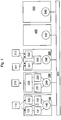
- Fig. 1 shows a basic system structure that can be used within the scope of the invention.
- the system structure shown is designed viewed topologically as a line, although a star topology or any mixed forms are also conceivable.
- a first bus participant is a monitoring module, e.g. a safety-related master, 100, hereinafter also referred to as a safety master, which in the present example is also the bus master, although this is not mandatory within the scope of the invention. This can generally be a specific, correspondingly specified security participant.
- a second and third bus subscriber is a safety-oriented slave output subscriber 200, also referred to below as an output module or safety output slave, or a safety-oriented slave input subscriber 300, also referred to below as a safety input slave.
- a fourth and fifth bus subscriber is a non-safety-oriented slave output subscriber 400, also referred to below as an output slave, or a non-safety-oriented slave input subscriber 500, also referred to as an input slave below.
- Safety-related participants i.e. participants who process safety-relevant process data, and non-safety-related participants can thus be mixed and also arranged as required.
- an emergency stop switch 110 is connected to the safety master 100, the safety-related input information of which the participant 100 receives redundantly via two inputs 121 and 122 and initially via two redundant inputs, depending on the protocol Processing channels 131 and 132 processed before a signal coupling to the bus 600 takes place.
- a motor 210 is connected to the safety output slave 200, whereby the participant 200, after a signal decoupling from the bus 600, initially carries out protocol-specific processing via two redundant processing channels 231 and 232 and sends the safety-relevant output information to the motor 210 via an output 220 .
- a protective door 311 and a speed sensor 312, for example, are connected to the safety input slave 300, the safety-relevant input information of which the participant 300 receives redundantly via two inputs 321 and 322 and processes it in a protocol-specific manner via a processing channel 330 before a signal is coupled to the bus 600.
- a safety-related function is therefore usually implemented using redundant processing, for example through two separate hardware channels, with the respective interface 140, 240, 340, 440 or 540 of a participant to the bus 600 usually only being implemented as a single channel is.
- this also enables twice the number of participants to be operated on the bus, in particular with regard to bus load, current consumption and capacity. Errors caused by the bus coupling, e.g. based on line drivers, galvanic isolation, can usually be recognized by the line protocol used.
- the processing unit of the safety-related subscribers does not necessarily have to be designed with two channels on the hardware side, but in many cases it is also sufficient if the software is designed with two channels.
- the bus 600 now provides the common data line for the method and transmission system according to the invention for sending and receiving all data, in particular process data.
- a LIN bus LIN: Local Interconnect Network
- a transmission system works in which, during certain data cycles, a master reads out protocol-specific data from field devices connected via subscribers and writes them into them during subsequent data cycles. with about 19.2 to 38 kbd.
- process input and output data are also transmitted, for example, at a fixed interval, each offset by half the bus cycle time.
- a transmission protocol for, for example, a cyclical transmission of process input and output data therefore often uses two different data exchange services, also referred to below as data exchange mode.
- a bus cycle consequently comprises a data cycle based on a PD read service and a subsequent data cycle based on a PD write service.
- a master When transferring process output data, a master basically sends all data for the connected field devices to the participants connected to it with the PD-Write service and then determines a CRC (Cyclic Redundancy Check), which it also transfers.
- the transmission system is expediently designed in such a way that all connected subscribers read all of the information transmitted in this way and preferably also form a CRC, which they use with the received CRC from the master compare, so that in the event of an error, an error message is generated and, for example, selected participants or individual field devices are transferred to a safe state.
- the master When transferring the process input data, the master first sends a broadcast address followed by a function code for a PD read service, for example.
- the other connected subscribers then place data from their connected field devices, that is to say in particular their process input data, bit by bit on the data line in the time slots provided for this in each case.
- the participants are in turn able to recognize all data by listening in on the data line and to calculate a CRC for this.
- FIG. 3 shows a block diagram of a monitoring system with an output module 201 and a monitoring module 203, which is in bidirectional connection with the output module 201.
- the monitoring system further comprises an output device 205, which is connected downstream of the output module 201, and a pass-through device 207, which is connected downstream of the monitoring module 203 and whose output is connected to the output device 205.
- the output device 205 comprises an output for outputting an output signal in response to a control signal which the output module 201 generates on the basis of an input signal supplied by the monitoring module 203. Before this, the output module 201 transmits the control signal for the purpose of checking to the monitoring module 203, which checks it for a deviation from an expected control signal.
- the monitoring module 203 instructs the penetration device 207, for example by means of a penetration signal, to output the output signal prevent.
- the penetration device 207 acts, for example, directly on the output device 205 and, for example, interrupts its control or data path in order to prevent the output of the output signal.
- the modules 201, 203, 205 and 207 do not necessarily have to be implemented in spatially separate designs. It is also conceivable that they are implemented on a printed circuit board. Instead of the bus system, a separate connection can also be provided for communication, e.g. across isolating distances.
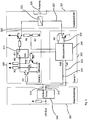
- Fig. 3 shows an output module with a bus coupling 301, a microcontroller circuit 303, a pass-through device 305 and an output device 307.
- the bus coupling 301 comprises an input to which, for example, a LIN bus can be coupled.
- the input is connected to a LIN bus driver 309, which has two connections 313 and 315.
- the connection 313 is connected via an input resistor R 1 of the penetration device 305 to a gate connection of a transistor T 1 of the penetration device 305.
- the transistor T 1 also has a first connection, for example an emitter connection, which is connected to ground.
- a second connection of the transistor T 1 for example a collector connection, is connected to a clock input A of a flip-flop 317, for example a monoflop.
- the second output of the transistor T 1 is connected to ground via a capacitor C 1 and to a supply potential via a resistor R 2.
- the flip-flop 317 further comprises a data input MR, which is connected to a second connection, for example a Collector connection of a second transistor T 2 is connected.
- a first connection of the transistor T 2 for example an emitter connection, is connected to ground.
- the data input MR can also be connected to a supply potential via a resistor R 3.
- a gate connection of the transistor T 2 is connected to a connection of the microcontroller 319 of the microcontroller circuit 303 via a resistor R 4.
- An output Q of the flip-flop 317 is connected via a resistor R 5 to a gate terminal of a third transistor T 3 , the first terminal of which, for example an emitter terminal, can be connected to a supply potential, and the second terminal of which can be connected to another via a resistor R 6 Port of the microcontroller 319 is connected.
- the resistor R 6 is connected to ground via a resistor R 7.
- the second connection of the third transistor T 3 simultaneously forms an output 323 of the penetration device 305, which is connected, for example, to an energy supply input of a relay 325 of the output device 307.
- the relay 325 includes a further path 327, which can be, for example, a data path or a control path.
- the relay 325 is also coupled to a switch 329.
- the switch 329 bridges two contacts as a function of a relay state, and an output signal can only be output when the switch is closed.
- the data path 327 of the relay 325 is connected to a second connection of a transistor T 4 , for example to a collector connection.
- the transistor T 4 also includes a second connection, for example an emitter connection, which is connected to ground.
- An output 329 of the microcontroller 319 is connected to a gate of the transistor T 4 .
- Another connection of the microcontroller 319 is furthermore connected to the second connection of the transistor T 4 via a resistor R 8 .
- connection 313 of the bus driver 309 is also connected to an input connection 331 of the microcontroller 319.
- an output connection 333 of the microcontroller is connected to connection 315.
- the microcontroller 319 receives data, for example an input signal, via the input connection 331 from an in Fig. 3 Monitoring module, not shown, and generates a control signal on its basis, which is fed to relay 325 via data path 327, for example. Before this, however, the microcontroller 319 sends the control signal to the monitoring module, not shown, via the output connection 333.
- the monitoring module checks whether the control signal corresponds to a control signal to be expected, for example on the basis of the input signal, ie the input data.
- the monitoring module transmits a penetration signal to the penetration device 305 via the connection 313 of the driver 309, on the basis of which, for example, as an alternative to the present invention, the energy supply of the relay 325 is interrupted, thereby closing the switch 329 is prevented or prevented. This prevents the output signal from being output.
- the structure of the in Fig. 3 The underlying concept shown in the output module is two-channel.
- the first channel is formed by the microcontroller circuit 303, while the penetration device 305 can be understood as a second channel, for example as an auxiliary channel.
- channel 2 that is to say the access device 305, of the output module is not necessarily a fully-fledged one Channel executed.
- the actual safety function is implemented, for example, by the microcontroller 319 of the microcontroller circuit 303.
- the microcontroller 319 can also be provided to implement the functional implementation of the bus protocol, the physical bus coupling, for example, by the in Fig. 3 LIN bus driver 309 shown can be produced.
- the processing of the safety function can begin with the received data.
- the microcontroller 329 controls the output device 307 (output stage) through the transistor T 4 , which can have a relay by way of example.
- the resistor R 8 is used to monitor the output stage 307, a monitoring result being published as a safety PDC by means of the microcontroller 319 in the next data cycle.
- the monitoring module (not shown) is able to check the microcontroller 319 and its output due to the known safety functions and the input data or input signals. If a discrepancy is detected, the monitoring module switches the system into a safe state by means of the superimposed security mechanism implemented by means of the access device 305.
- an analog output stage can also be used, for example, which is designed for a range between 4 mA and 20 mA, with its output current being less than 3 mA in the event of an error.
- Fig. 4 shows an example of a bus timing with a transmission cycle 400 that can be divided into three phases.
- the first phase 401 useful data are transmitted.
- the second phase 403 is used to check data on the frame and PDC level. If, for example, none of the participants discovers an error, the data signal of the LIN bus remains in the high-level state, which corresponds to a "high". If an error is detected, the subscriber concerned sends an error code, as is shown with the aid of data section 405. If no error was detected in the entire transmission and processing cycle including the checking of the output states of the safety outputs, the monitoring module, i.e. the master, generates an enable signal for the outputs, which is triggered by the monoflop 317 Fig. 3 is evaluated. The data verification takes place in section 403, for example. The output release is indicated by section 409.
- the monoflop 317 can, for example, be retriggered with a mono time of 30 ms. For example, it can only be triggered when the bus signal assumes a low level state, so-called “low”, represented by the output enable 409, for at least 700 microseconds, for example. However, this is not guaranteed during data transmission with a baud rate of at least 14400 baud, because the transmission of a stop bit at the end of each character forces at least a logical "1".
- the quiescent level of the LIN bus is also a logic "1", so that prolonged bus inactivity does not result in triggering.
- the "1" level on the LIN bus means that the in Fig. 3 illustrated transistor T 1 is turned on, which prevents or prevents charging of the capacitor C 1, so that no negative edge can occur at the input of the monoflop 317. Only a logical “low” blocks the transistor and leads to the capacitor C 1 being charged by the resistor R 2. After about 700 microseconds, the capacitor C 1 is charged to, for example, the “high” switching level of the monostable multivibrator 317, so that a triggering edge is generated at the monostable multivibrator 317 when the LIN bus signal changes from “low” to “high” . The output / Q is then switched to "Low", which leads to the output stage 307 being enabled.
- the microcontroller can check the switching transistor T 4 through the resistor R 8.
- the voltage divider comprising the resistors R 6 and R 7 is used to check the penetration device 305, which is implemented, for example, as an auxiliary channel. For the check, it can be advantageous to reset the monoflop 317 via the transistor T 2 , which leads to the transistor T 3 being blocked and thus the output stage 307 to be switched off.
- Fig. 5 shows a block diagram of an output module with a microcontroller circuit 501 and a penetration device 503.
- the microcontroller circuit 501 comprises a microcontroller 505 with a further penetration device 507.
- An input 509 of the output module is connected to a flip-flop 511, for example a monoflop, of the penetration device 503.
- the flip-flop 511 also has an output which, for example, with an in Fig. 5 output device, not shown, can be coupled.
- the input 509 is also connected to a reception input 513 of the microcontroller 505 and to an input 515 of the further penetration device 507.
- This comprises an input component 517 which is connected to an input of a flip-flop 519, for example a monoflop.
- a The output of the flip-flop 519 is connected to a connection of an output driver 521, for example an operational amplifier, of the further pass-through device 507.
- An output of the output driver 521 is connected to a gate of a transistor T 4 , the first connection of which, for example a collector connection, forms an output 523 of the microcontroller circuit 501.
- a second connection of the transistor T 4 for example a collector connection, is connected to ground.
- the second connection of the transistor T 4 is connected to an input element 525, for example an input driver, of the microcontroller 505 via a resistor R 8 by means of feedback.
- An output of the input element 525 is connected to a diagnostic element 527, which as in FIG Fig. 5 is connected to the flip-flop 511 shown.
- An output of the diagnostic element 527 is connected to a PDC producer 529, the output of which is connected to a bus element 531.
- the bus element 531 is also coupled to a UART 533 (UART: Universal Asynchronous Receiver / Transmitter). As in Fig. 5 the receiving input 513 is shown connected to an input of the UART 533.
- the UART 533 also has an output 535 which forms an output of the microcontroller circuit 501.
- the bus protocol element 531 is coupled to a PDC consumer 537, the output of which is connected to a safety function block 538.
- the safety function block 538 has an output which is connected to an input of the output element 5
- the further access device 507 can be implemented, for example, in software, while the access device 503 can be implemented in hardware.
- Further components implemented in hardware can include the UART element 533 and the input elements 517, 525 and the Be output element 521.
- the elements 527, 529, 531, 537, 519 and 538, on the other hand, can be implemented in software.
- the main signal path of the safety function leads from the UART block 533 through a protocol stack that is implemented in the bus protocol element 531.
- the data exchange between the bus protocol and the processing unit takes place, for example, by means of two buffers 529 and 537, the input data of the safety function being stored in the consumer PDC buffer 537. Accordingly, the output and status data are transferred to a monitoring module by the producer buffer 529, which is implemented in Fig. 5 is not shown, transferred.
- the output driver 521 of the microcontroller 505 has, as in FIG Fig. 5 shown, two inputs, whereby the safety function only uses the data or control input, for example. If the output driver 521 is enabled by the second input, this state is visible to the transistor T 4.
- the monoflop 519 realizes, for example, the same function as the pass-through device 503, which can also be referred to as a second channel or an auxiliary channel, with the difference that it can be implemented almost completely in software and thus ensures diversity.
- the pass-through device 503 and its monoflop function can also be implemented by a software function. This is particularly advantageous when a second microcontroller is used for more complex output modules.
Claims (8)
- Système de surveillance comprenant :un module de sortie (201) conçu pour générer un signal de commande en réponse à un signal d'entrée ;un module de surveillance (203) conçu pour générer le signal d'entrée pour le module de sortie (201), où le module de surveillance (203) et le module de sortie (201) sont des modules séparés ;un dispositif d'émission (205) conçu pour l'émission d'un signal de sortie en réponse au signal de commande ; etun dispositif de passage (207) pour interdire l'émission du signal de sortie ;dans lequel le module de sortie (201) est conçu pour envoyer le signal de commande au module de surveillance (203) et le module de surveillance (203) est conçu pour recevoir le signal de commande ;dans lequel le module de surveillance (203) est conçu pour comparer le signal de commande avec un signal de commande attendu en fonction du signal d'entrée afin d'examiner le signal de commande et de détecter l'existence d'un écart,caractérisé en ce quele module de surveillance (203) est conçu, lors de l'existence d'un écart entre le signal de commande et le signal de commande attendu, pour ordonner au dispositif de passage (207), par l'envoi d'un signal de passage au dispositif de passage (207), d'interdire l'émission du signal de sortie, où le dispositif de passage (207) est conçu pour interdire l'émission du signal de sortie en interrompant un chemin de commande ou de données du dispositif d'émission (205), et où le module de surveillance (203) est conçu pour générer un signal de validation et pour l'envoyer au module de sortie (201) au cas où le signal de commande correspond au signal de commande attendu, où le signal de validation indique la validation du signal de sortie.
- Système de surveillance selon la revendication 1, dans lequel le module de surveillance (203) et le module de sortie (201) ou le dispositif de passage (207) sont conçus pour communiquer par l'intermédiaire d'un réseau de communication, plus particulièrement par l'intermédiaire d'un bus de communication.
- Système de surveillance selon l'une des revendications précédentes, dans lequel le dispositif de passage (207) est disposé dans le module de surveillance (203) ou dans le module de sortie (201) .
- Système de surveillance selon l'une des revendications précédentes, dans lequel le dispositif d'émission (205) comprend un relais ou un étage de sortie analogique avec un chemin de données pour la réception du signal de commande et un chemin d'alimentation en énergie pour l'alimentation du dispositif d'émission en énergie électrique.
- Système de surveillance selon l'une des revendications précédentes, dans lequel le dispositif de passage (207) comprend un étage à bascule monostable, plus particulièrement une bascule ou une bascule monostable, dans lequel le dispositif d'émission (205) comprend un chemin de données et un chemin d'alimentation en énergie et dans lequel une sortie de l'étage à bascule est couplée, plus particulièrement par l'intermédiaire d'un transistor de sortie, avec le chemin de données, afin d'agir sur le chemin de données, plus particulièrement en réponse à un signal de passage pouvant être appliqué à une entrée de l'étage à bascule.
- Système de surveillance selon l'une des revendications précédentes, dans lequel le dispositif de passage (207) est conçu pour mettre le dispositif d'émission (205) dans un mode de blocage en réponse à un signal de passage.
- Système de surveillance selon l'une des revendications précédentes, dans lequel le module de sortie (201) comprend un micro-contrôleur qui est conçu pour recevoir le signal d'entrée et générer le signal de commande.
- Procédé de surveillance d'un module de sortie (201) par un module de surveillance (203) séparé, dans lequel le module de sortie (201) génère un signal de commande en réponse à un signal d'entrée et l'envoie au module de surveillance (203), dans lequel le module de surveillance (203) reçoit le signal de commande et génère le signal d'entrée pour le module de sortie (201), dans lequel, en réponse au signal de commande, un signal de sortie est émis par un dispositif d'émission (205), et dans lequel le signal de commande est comparé, par le module de surveillance (203), avec un signal de commande attendu en fonction du signal d'entrée, afin d'examiner le signal de commande et de détecter l'existence d'un écart,caractérisé en ce quelors de l'existence d'un écart entre le signal de commande et le signal de commande attendu, il est ordonné à un dispositif de passage (207), par le module de surveillance (203), au moyen d'un signal de passage, d'interdire l'émission du signal de sortie, et dans lequel un chemin de commande ou de données du dispositif d'émission (205) est interrompu par le dispositif de passage (207) afin d'interdire l'émission du signal de sortie et dans lequel un signal de validation est généré par le module de surveillance (203) et envoyé au module de sortie (201), dans le cas où le signal de commande correspond au signal de commande attendu et dans lequel le signal de validation indique la validation du signal de sortie.
Applications Claiming Priority (2)
| Application Number | Priority Date | Filing Date | Title |
|---|---|---|---|
| DE102008029948.0A DE102008029948B4 (de) | 2008-06-26 | 2008-06-26 | Überwachungssystem |
| PCT/EP2009/004516 WO2009156122A1 (fr) | 2008-06-26 | 2009-06-23 | Système de surveillance |
Publications (2)
| Publication Number | Publication Date |
|---|---|
| EP2297619A1 EP2297619A1 (fr) | 2011-03-23 |
| EP2297619B1 true EP2297619B1 (fr) | 2021-11-03 |
Family
ID=41090591
Family Applications (1)
| Application Number | Title | Priority Date | Filing Date |
|---|---|---|---|
| EP09768971.5A Active EP2297619B1 (fr) | 2008-06-26 | 2009-06-23 | Système de surveillance |
Country Status (7)
| Country | Link |
|---|---|
| US (1) | US8744805B2 (fr) |
| EP (1) | EP2297619B1 (fr) |
| JP (1) | JP5490112B2 (fr) |
| CN (1) | CN102077148B (fr) |
| DE (1) | DE102008029948B4 (fr) |
| RU (1) | RU2504813C2 (fr) |
| WO (1) | WO2009156122A1 (fr) |
Families Citing this family (6)
| Publication number | Priority date | Publication date | Assignee | Title |
|---|---|---|---|---|
| DE102012016269A1 (de) | 2012-08-17 | 2014-02-20 | Abb Ag | Elektrische Maschine mit einer Überwachungseinrichtung |
| EP2767877B1 (fr) * | 2013-02-13 | 2016-07-06 | Phoenix Contact GmbH & Co. KG | Système de commande et de transmission de données pour la transmission de données liées à la sécurité via un bus de terrain |
| DE102013217063A1 (de) * | 2013-08-27 | 2015-03-05 | E.G.O. Elektro-Gerätebau GmbH | Haushaltsgerätesteuerung |
| CN104702333B (zh) * | 2015-01-14 | 2017-10-03 | 西安爱生技术集团公司 | 一种无人机测控信号分配器及分配方法 |
| DE102016106531A1 (de) * | 2016-04-08 | 2017-10-12 | Eaton Electrical Ip Gmbh & Co. Kg | Busteilnehmer und Verfahren zum Betreiben eines Busteilnehmers |
| DE102020128026A1 (de) * | 2020-10-23 | 2022-04-28 | Pilz Gmbh & Co. Kg | Steuervorrichtung mit Schutzmodul |
Family Cites Families (30)
| Publication number | Priority date | Publication date | Assignee | Title |
|---|---|---|---|---|
| US2883255A (en) * | 1954-04-28 | 1959-04-21 | Panellit Inc | Automatic process logging system |
| US3237164A (en) * | 1962-06-29 | 1966-02-22 | Control Data Corp | Digital communication system for transferring digital information between a plurality of data processing devices |
| US3337773A (en) * | 1964-11-06 | 1967-08-22 | Barber Colman Co | Overload prevention for control systems |
| US3421069A (en) * | 1966-08-04 | 1969-01-07 | Brunswick Corp | Regulated power supply including a blocking oscillator and trigger means to turn off the oscillator |
| CA850273A (en) * | 1967-07-06 | 1970-08-25 | Charles J. Clarke, Jr. | D. d. c. interfacing circuitry |
| US3516072A (en) * | 1967-09-18 | 1970-06-02 | Susquehanna Corp | Data collection system |
| CA825823A (en) * | 1968-02-09 | 1969-10-21 | A. Hogan James | Electronic process controller |
| DE3538484A1 (de) * | 1985-10-25 | 1987-05-07 | Siemens Ag | Verfahren zur ueberpruefung von schutzbefehl-uebertragungssystemen im on-line-betrieb |
| RU2099764C1 (ru) * | 1994-11-30 | 1997-12-20 | Акционерное общество открытого типа "Хлебокомбинат Восход" | Ограничитель технологических режимов |
| JP3297249B2 (ja) | 1995-05-26 | 2002-07-02 | 三菱電機株式会社 | 分散型リモートi/o式制御システムの制御方法 |
| US6243629B1 (en) | 1996-04-19 | 2001-06-05 | Honda Giken Kogyo Kabushiki Kaisha | Electronic control unit for automotive vehicles |
| JP3716948B2 (ja) * | 1996-04-19 | 2005-11-16 | 本田技研工業株式会社 | 車載用電子制御ユニット |
| DE19718284C2 (de) * | 1997-05-01 | 2001-09-27 | Kuka Roboter Gmbh | Verfahren und Vorrichtung zum Überwachen einer Anlage mit mehreren Funktionseinheiten |
| US6028491A (en) * | 1998-04-29 | 2000-02-22 | Atmel Corporation | Crystal oscillator with controlled duty cycle |
| DE19860358B4 (de) | 1998-12-24 | 2008-05-08 | Wratil, Peter, Dr. | Verfahren zur Fehlerunterdrückung bei Ausgabeeinheiten in Steuerungseinrichtungen |
| DE19913279B4 (de) | 1999-03-24 | 2006-07-27 | Wratil, Peter, Dr. | Steuerungseinrichtung mit Überwachungseinheit zur Fehlererkennung und Fehlerunterdrückung |
| JP3752884B2 (ja) * | 1999-04-19 | 2006-03-08 | 三菱電機株式会社 | 自己監視機能付き車載用電子制御装置 |
| JP3716664B2 (ja) * | 1999-04-19 | 2005-11-16 | 三菱電機株式会社 | 自己監視機能付き車載用電子制御装置 |
| DE10008434A1 (de) | 2000-02-23 | 2001-09-20 | Phoenix Contact Gmbh & Co | Verfahren und Vorrichtung zur Sicherheitsüberwachung einer Steuereinrichtung |
| RU32615U1 (ru) * | 2003-04-28 | 2003-09-20 | Кушев Дмитрий Владимирович | Система безопасного управления и контроля |
| JP4451712B2 (ja) * | 2004-05-18 | 2010-04-14 | 富士通マイクロエレクトロニクス株式会社 | データ転送装置、および転送異常状態検出方法。 |
| CN1588762A (zh) * | 2004-09-28 | 2005-03-02 | 张瑞棉 | 微电节能环保发电机 |
| DE102004061013A1 (de) | 2004-12-18 | 2006-07-06 | Bosch Rexroth Aktiengesellschaft | Sichere Eingabe-/Ausgabe-Baugruppe für eine Steuerung |
| US8055814B2 (en) | 2005-03-18 | 2011-11-08 | Rockwell Automation Technologies, Inc. | Universal safety I/O module |
| DE502006007907D1 (de) | 2005-08-02 | 2010-10-28 | Phoenix Contact Gmbh & Co | Messvorrichtung zum Messen eines periodischen Analogsignals |
| DE102006001805A1 (de) | 2006-01-12 | 2007-07-19 | Phoenix Contact Gmbh & Co. Kg | Sicherheitsvorrichtung zum mehrkanaligen Steuern einer sicherheitstechnischen Einrichtung |
| DE102006020793A1 (de) | 2006-05-03 | 2007-11-08 | Ab Skf | Schaltungsanordnung und Verfahren zum Betrieb einer Schaltungsanordnung |
| KR100809703B1 (ko) * | 2006-09-22 | 2008-03-06 | 삼성전자주식회사 | 안정적으로 신호를 전송하는 패스 게이트 회로 및 그제어방법 |
| WO2008037495A2 (fr) | 2006-09-28 | 2008-04-03 | Pepperl + Fuchs Gmbh | Système de bus et procédé permettant son fonctionnement |
| DE102006056420B4 (de) | 2006-11-28 | 2012-11-29 | Wago Verwaltungsgesellschaft Mbh | Sicherheitsmodul und Automatisierungssystem |
-
2008
- 2008-06-26 DE DE102008029948.0A patent/DE102008029948B4/de active Active
-
2009
- 2009-06-23 RU RU2011102770/08A patent/RU2504813C2/ru not_active IP Right Cessation
- 2009-06-23 CN CN200980124498.XA patent/CN102077148B/zh active Active
- 2009-06-23 JP JP2011515190A patent/JP5490112B2/ja not_active Expired - Fee Related
- 2009-06-23 US US12/997,748 patent/US8744805B2/en active Active
- 2009-06-23 EP EP09768971.5A patent/EP2297619B1/fr active Active
- 2009-06-23 WO PCT/EP2009/004516 patent/WO2009156122A1/fr active Application Filing
Also Published As
| Publication number | Publication date |
|---|---|
| JP2011525667A (ja) | 2011-09-22 |
| EP2297619A1 (fr) | 2011-03-23 |
| RU2011102770A (ru) | 2012-08-10 |
| RU2504813C2 (ru) | 2014-01-20 |
| US20110128046A1 (en) | 2011-06-02 |
| DE102008029948B4 (de) | 2018-08-30 |
| CN102077148A (zh) | 2011-05-25 |
| US8744805B2 (en) | 2014-06-03 |
| WO2009156122A1 (fr) | 2009-12-30 |
| DE102008029948A1 (de) | 2010-01-21 |
| CN102077148B (zh) | 2015-05-13 |
| JP5490112B2 (ja) | 2014-05-14 |
Similar Documents
| Publication | Publication Date | Title |
|---|---|---|
| EP1738382B2 (fr) | Dispositif de commutation de securite pour circuit de securite | |
| EP2297619B1 (fr) | Système de surveillance | |
| WO2004029737A1 (fr) | Systeme de dispositifs de commande redondant | |
| EP2145430B1 (fr) | Procédé et système de transmission cyclique fiable de données de processus | |
| EP2356528B1 (fr) | Procédé pour transférer des données dans un système de commande automatisé | |
| WO2016008948A1 (fr) | Système de commande et de transmission de données, module de passerelle, module e/a et procédé de commande de processus | |
| EP1533673A2 (fr) | système de commande | |
| WO2008053039A1 (fr) | Dispositif et procédé pour la manipulation de messages de communication | |
| EP1989470B1 (fr) | Concept de sécurité pour un dispositif de positionnement à engrenage | |
| DE102006002824B4 (de) | Verfahren und Vorrichtung zur Umwandlung mehrkanalig vorliegender Nachrichten in eine einkanalige sichere Nachricht | |
| EP2491492A1 (fr) | Système d'automatisation et procédé pour faire fonctionner un système d'automatisation | |
| WO1999036840A1 (fr) | Entree et sortie a securite intrinseque de signaux de processus | |
| EP1672446B1 (fr) | Module d'entrée/sortie sécurisé pour un controleur | |
| EP3100121A1 (fr) | Procédé et dispositif pour déconnecter en toute sécurité une charge électrique | |
| DE102012210126A1 (de) | Verfahren zum Betreiben einer Netzwerkanordnung, Netzwerkeinrichtung und Netzwerkanordnung | |
| DE102011051629B3 (de) | Sicherheitsbussystem | |
| DE10232272B4 (de) | Verfahren zum Betrieb einer Vorrichtung fü ein Sicherheitssystem | |
| EP1064590B1 (fr) | Telegramme de donnees abrege d'un systeme d'automatisation | |
| EP2767877B1 (fr) | Système de commande et de transmission de données pour la transmission de données liées à la sécurité via un bus de terrain | |
| EP3915227B1 (fr) | Dispositif d'émission/réception pour un poste d'abonné d'un système de bus série et procédé de communication dans un système de bus série | |
| EP3742680B1 (fr) | Dispositif distributeur et procédé correspondant | |
| DE102022000991A1 (de) | Automatisierungssystem und Verfahren zum Betrieb eines Automatisierungssystem | |
| DE102008064761B3 (de) | Verfahren und Vorrichtung zum Prüfen einer asynchronenÜbertragung von Steuersignalen | |
| DE102009028103A1 (de) | Verfahren zur Durchführung einer Kommunikation | |
| DD240457A1 (de) | Informationsverarbeitungssystem mit hohem zuverlaessigkeits- und sicherheitsniveau |
Legal Events
| Date | Code | Title | Description |
|---|---|---|---|
| PUAI | Public reference made under article 153(3) epc to a published international application that has entered the european phase |
Free format text: ORIGINAL CODE: 0009012 |
|
| 17P | Request for examination filed |
Effective date: 20110114 |
|
| AK | Designated contracting states |
Kind code of ref document: A1 Designated state(s): AT BE BG CH CY CZ DE DK EE ES FI FR GB GR HR HU IE IS IT LI LT LU LV MC MK MT NL NO PL PT RO SE SI SK TR |
|
| AX | Request for extension of the european patent |
Extension state: AL BA RS |
|
| DAX | Request for extension of the european patent (deleted) | ||
| 17Q | First examination report despatched |
Effective date: 20160701 |
|
| STAA | Information on the status of an ep patent application or granted ep patent |
Free format text: STATUS: EXAMINATION IS IN PROGRESS |
|
| R17C | First examination report despatched (corrected) |
Effective date: 20160701 |
|
| STAA | Information on the status of an ep patent application or granted ep patent |
Free format text: STATUS: EXAMINATION IS IN PROGRESS |
|
| GRAP | Despatch of communication of intention to grant a patent |
Free format text: ORIGINAL CODE: EPIDOSNIGR1 |
|
| STAA | Information on the status of an ep patent application or granted ep patent |
Free format text: STATUS: GRANT OF PATENT IS INTENDED |
|
| RIC1 | Information provided on ipc code assigned before grant |
Ipc: G06F 17/40 20060101ALN20210511BHEP Ipc: G05B 9/02 20060101ALI20210511BHEP Ipc: G05B 19/042 20060101AFI20210511BHEP |
|
| INTG | Intention to grant announced |
Effective date: 20210526 |
|
| RBV | Designated contracting states (corrected) |
Designated state(s): AT BE BG CH CY CZ DK EE ES FI FR GB GR HR HU IE IS IT LI LT LU LV MC MK MT NL NO PL PT RO SE SI SK TR |
|
| REG | Reference to a national code |
Ref country code: DE Ref legal event code: R108 |
|
| GRAS | Grant fee paid |
Free format text: ORIGINAL CODE: EPIDOSNIGR3 |
|
| GRAA | (expected) grant |
Free format text: ORIGINAL CODE: 0009210 |
|
| STAA | Information on the status of an ep patent application or granted ep patent |
Free format text: STATUS: THE PATENT HAS BEEN GRANTED |
|
| AK | Designated contracting states |
Kind code of ref document: B1 Designated state(s): AT BE BG CH CY CZ DK EE ES FI FR GB GR HR HU IE IS IT LI LT LU LV MC MK MT NL NO PL PT RO SE SI SK TR |
|
| REG | Reference to a national code |
Ref country code: GB Ref legal event code: FG4D Free format text: NOT ENGLISH |
|
| REG | Reference to a national code |
Ref country code: AT Ref legal event code: REF Ref document number: 1444525 Country of ref document: AT Kind code of ref document: T Effective date: 20211115 Ref country code: CH Ref legal event code: EP |
|
| REG | Reference to a national code |
Ref country code: IE Ref legal event code: FG4D Free format text: LANGUAGE OF EP DOCUMENT: GERMAN |
|
| REG | Reference to a national code |
Ref country code: LT Ref legal event code: MG9D |
|
| REG | Reference to a national code |
Ref country code: NL Ref legal event code: MP Effective date: 20211103 |
|
| PG25 | Lapsed in a contracting state [announced via postgrant information from national office to epo] |
Ref country code: LT Free format text: LAPSE BECAUSE OF FAILURE TO SUBMIT A TRANSLATION OF THE DESCRIPTION OR TO PAY THE FEE WITHIN THE PRESCRIBED TIME-LIMIT Effective date: 20211103 Ref country code: FI Free format text: LAPSE BECAUSE OF FAILURE TO SUBMIT A TRANSLATION OF THE DESCRIPTION OR TO PAY THE FEE WITHIN THE PRESCRIBED TIME-LIMIT Effective date: 20211103 Ref country code: BG Free format text: LAPSE BECAUSE OF FAILURE TO SUBMIT A TRANSLATION OF THE DESCRIPTION OR TO PAY THE FEE WITHIN THE PRESCRIBED TIME-LIMIT Effective date: 20220203 |
|
| PG25 | Lapsed in a contracting state [announced via postgrant information from national office to epo] |
Ref country code: IS Free format text: LAPSE BECAUSE OF FAILURE TO SUBMIT A TRANSLATION OF THE DESCRIPTION OR TO PAY THE FEE WITHIN THE PRESCRIBED TIME-LIMIT Effective date: 20220303 Ref country code: SE Free format text: LAPSE BECAUSE OF FAILURE TO SUBMIT A TRANSLATION OF THE DESCRIPTION OR TO PAY THE FEE WITHIN THE PRESCRIBED TIME-LIMIT Effective date: 20211103 Ref country code: PT Free format text: LAPSE BECAUSE OF FAILURE TO SUBMIT A TRANSLATION OF THE DESCRIPTION OR TO PAY THE FEE WITHIN THE PRESCRIBED TIME-LIMIT Effective date: 20220303 Ref country code: PL Free format text: LAPSE BECAUSE OF FAILURE TO SUBMIT A TRANSLATION OF THE DESCRIPTION OR TO PAY THE FEE WITHIN THE PRESCRIBED TIME-LIMIT Effective date: 20211103 Ref country code: NO Free format text: LAPSE BECAUSE OF FAILURE TO SUBMIT A TRANSLATION OF THE DESCRIPTION OR TO PAY THE FEE WITHIN THE PRESCRIBED TIME-LIMIT Effective date: 20220203 Ref country code: NL Free format text: LAPSE BECAUSE OF FAILURE TO SUBMIT A TRANSLATION OF THE DESCRIPTION OR TO PAY THE FEE WITHIN THE PRESCRIBED TIME-LIMIT Effective date: 20211103 Ref country code: LV Free format text: LAPSE BECAUSE OF FAILURE TO SUBMIT A TRANSLATION OF THE DESCRIPTION OR TO PAY THE FEE WITHIN THE PRESCRIBED TIME-LIMIT Effective date: 20211103 Ref country code: HR Free format text: LAPSE BECAUSE OF FAILURE TO SUBMIT A TRANSLATION OF THE DESCRIPTION OR TO PAY THE FEE WITHIN THE PRESCRIBED TIME-LIMIT Effective date: 20211103 Ref country code: GR Free format text: LAPSE BECAUSE OF FAILURE TO SUBMIT A TRANSLATION OF THE DESCRIPTION OR TO PAY THE FEE WITHIN THE PRESCRIBED TIME-LIMIT Effective date: 20220204 Ref country code: ES Free format text: LAPSE BECAUSE OF FAILURE TO SUBMIT A TRANSLATION OF THE DESCRIPTION OR TO PAY THE FEE WITHIN THE PRESCRIBED TIME-LIMIT Effective date: 20211103 |
|
| PG25 | Lapsed in a contracting state [announced via postgrant information from national office to epo] |
Ref country code: SK Free format text: LAPSE BECAUSE OF FAILURE TO SUBMIT A TRANSLATION OF THE DESCRIPTION OR TO PAY THE FEE WITHIN THE PRESCRIBED TIME-LIMIT Effective date: 20211103 Ref country code: RO Free format text: LAPSE BECAUSE OF FAILURE TO SUBMIT A TRANSLATION OF THE DESCRIPTION OR TO PAY THE FEE WITHIN THE PRESCRIBED TIME-LIMIT Effective date: 20211103 Ref country code: EE Free format text: LAPSE BECAUSE OF FAILURE TO SUBMIT A TRANSLATION OF THE DESCRIPTION OR TO PAY THE FEE WITHIN THE PRESCRIBED TIME-LIMIT Effective date: 20211103 Ref country code: DK Free format text: LAPSE BECAUSE OF FAILURE TO SUBMIT A TRANSLATION OF THE DESCRIPTION OR TO PAY THE FEE WITHIN THE PRESCRIBED TIME-LIMIT Effective date: 20211103 Ref country code: CZ Free format text: LAPSE BECAUSE OF FAILURE TO SUBMIT A TRANSLATION OF THE DESCRIPTION OR TO PAY THE FEE WITHIN THE PRESCRIBED TIME-LIMIT Effective date: 20211103 |
|
| PLBE | No opposition filed within time limit |
Free format text: ORIGINAL CODE: 0009261 |
|
| STAA | Information on the status of an ep patent application or granted ep patent |
Free format text: STATUS: NO OPPOSITION FILED WITHIN TIME LIMIT |
|
| 26N | No opposition filed |
Effective date: 20220804 |
|
| PG25 | Lapsed in a contracting state [announced via postgrant information from national office to epo] |
Ref country code: SI Free format text: LAPSE BECAUSE OF FAILURE TO SUBMIT A TRANSLATION OF THE DESCRIPTION OR TO PAY THE FEE WITHIN THE PRESCRIBED TIME-LIMIT Effective date: 20211103 |
|
| PG25 | Lapsed in a contracting state [announced via postgrant information from national office to epo] |
Ref country code: MC Free format text: LAPSE BECAUSE OF FAILURE TO SUBMIT A TRANSLATION OF THE DESCRIPTION OR TO PAY THE FEE WITHIN THE PRESCRIBED TIME-LIMIT Effective date: 20211103 |
|
| REG | Reference to a national code |
Ref country code: CH Ref legal event code: PL |
|
| REG | Reference to a national code |
Ref country code: BE Ref legal event code: MM Effective date: 20220630 |
|
| PG25 | Lapsed in a contracting state [announced via postgrant information from national office to epo] |
Ref country code: LU Free format text: LAPSE BECAUSE OF NON-PAYMENT OF DUE FEES Effective date: 20220623 Ref country code: LI Free format text: LAPSE BECAUSE OF NON-PAYMENT OF DUE FEES Effective date: 20220630 Ref country code: IE Free format text: LAPSE BECAUSE OF NON-PAYMENT OF DUE FEES Effective date: 20220623 Ref country code: CH Free format text: LAPSE BECAUSE OF NON-PAYMENT OF DUE FEES Effective date: 20220630 |
|
| PG25 | Lapsed in a contracting state [announced via postgrant information from national office to epo] |
Ref country code: IT Free format text: LAPSE BECAUSE OF FAILURE TO SUBMIT A TRANSLATION OF THE DESCRIPTION OR TO PAY THE FEE WITHIN THE PRESCRIBED TIME-LIMIT Effective date: 20211103 Ref country code: BE Free format text: LAPSE BECAUSE OF NON-PAYMENT OF DUE FEES Effective date: 20220630 |
|
| P01 | Opt-out of the competence of the unified patent court (upc) registered |
Effective date: 20230424 |
|
| PGFP | Annual fee paid to national office [announced via postgrant information from national office to epo] |
Ref country code: FR Payment date: 20230622 Year of fee payment: 15 |
|
| REG | Reference to a national code |
Ref country code: AT Ref legal event code: MM01 Ref document number: 1444525 Country of ref document: AT Kind code of ref document: T Effective date: 20220623 |
|
| PG25 | Lapsed in a contracting state [announced via postgrant information from national office to epo] |
Ref country code: AT Free format text: LAPSE BECAUSE OF NON-PAYMENT OF DUE FEES Effective date: 20220623 |
|
| PGFP | Annual fee paid to national office [announced via postgrant information from national office to epo] |
Ref country code: GB Payment date: 20230620 Year of fee payment: 15 |
|
| PG25 | Lapsed in a contracting state [announced via postgrant information from national office to epo] |
Ref country code: HU Free format text: LAPSE BECAUSE OF FAILURE TO SUBMIT A TRANSLATION OF THE DESCRIPTION OR TO PAY THE FEE WITHIN THE PRESCRIBED TIME-LIMIT; INVALID AB INITIO Effective date: 20090623 |
|
| PG25 | Lapsed in a contracting state [announced via postgrant information from national office to epo] |
Ref country code: MK Free format text: LAPSE BECAUSE OF FAILURE TO SUBMIT A TRANSLATION OF THE DESCRIPTION OR TO PAY THE FEE WITHIN THE PRESCRIBED TIME-LIMIT Effective date: 20211103 Ref country code: CY Free format text: LAPSE BECAUSE OF FAILURE TO SUBMIT A TRANSLATION OF THE DESCRIPTION OR TO PAY THE FEE WITHIN THE PRESCRIBED TIME-LIMIT Effective date: 20211103 |