EP2293394A2 - Verbindungsendgerät und Wechselstromadapter - Google Patents
Verbindungsendgerät und Wechselstromadapter Download PDFInfo
- Publication number
- EP2293394A2 EP2293394A2 EP10175540A EP10175540A EP2293394A2 EP 2293394 A2 EP2293394 A2 EP 2293394A2 EP 10175540 A EP10175540 A EP 10175540A EP 10175540 A EP10175540 A EP 10175540A EP 2293394 A2 EP2293394 A2 EP 2293394A2
- Authority
- EP
- European Patent Office
- Prior art keywords
- elastic contact
- contact pieces
- terminal
- connection terminal
- support part
- Prior art date
- Legal status (The legal status is an assumption and is not a legal conclusion. Google has not performed a legal analysis and makes no representation as to the accuracy of the status listed.)
- Granted
Links
- 230000002093 peripheral effect Effects 0.000 claims abstract description 19
- 230000000149 penetrating effect Effects 0.000 claims description 3
- 238000003780 insertion Methods 0.000 description 20
- 230000037431 insertion Effects 0.000 description 20
- 238000010586 diagram Methods 0.000 description 10
- 229910000679 solder Inorganic materials 0.000 description 10
- 239000000463 material Substances 0.000 description 6
- 239000000758 substrate Substances 0.000 description 4
- 229910000906 Bronze Inorganic materials 0.000 description 2
- 239000004593 Epoxy Substances 0.000 description 2
- OAICVXFJPJFONN-UHFFFAOYSA-N Phosphorus Chemical compound [P] OAICVXFJPJFONN-UHFFFAOYSA-N 0.000 description 2
- 238000005452 bending Methods 0.000 description 2
- 239000010974 bronze Substances 0.000 description 2
- 239000003990 capacitor Substances 0.000 description 2
- KUNSUQLRTQLHQQ-UHFFFAOYSA-N copper tin Chemical compound [Cu].[Sn] KUNSUQLRTQLHQQ-UHFFFAOYSA-N 0.000 description 2
- 239000011521 glass Substances 0.000 description 1
- 238000012986 modification Methods 0.000 description 1
- 230000004048 modification Effects 0.000 description 1
- ISWSIDIOOBJBQZ-UHFFFAOYSA-N phenol group Chemical group C1(=CC=CC=C1)O ISWSIDIOOBJBQZ-UHFFFAOYSA-N 0.000 description 1
Images





Classifications
-
- H—ELECTRICITY
- H01—ELECTRIC ELEMENTS
- H01R—ELECTRICALLY-CONDUCTIVE CONNECTIONS; STRUCTURAL ASSOCIATIONS OF A PLURALITY OF MUTUALLY-INSULATED ELECTRICAL CONNECTING ELEMENTS; COUPLING DEVICES; CURRENT COLLECTORS
- H01R13/00—Details of coupling devices of the kinds covered by groups H01R12/70 or H01R24/00 - H01R33/00
- H01R13/02—Contact members
- H01R13/10—Sockets for co-operation with pins or blades
- H01R13/11—Resilient sockets
- H01R13/111—Resilient sockets co-operating with pins having a circular transverse section
-
- H—ELECTRICITY
- H01—ELECTRIC ELEMENTS
- H01R—ELECTRICALLY-CONDUCTIVE CONNECTIONS; STRUCTURAL ASSOCIATIONS OF A PLURALITY OF MUTUALLY-INSULATED ELECTRICAL CONNECTING ELEMENTS; COUPLING DEVICES; CURRENT COLLECTORS
- H01R31/00—Coupling parts supported only by co-operation with counterpart
- H01R31/06—Intermediate parts for linking two coupling parts, e.g. adapter
- H01R31/065—Intermediate parts for linking two coupling parts, e.g. adapter with built-in electric apparatus
-
- H—ELECTRICITY
- H01—ELECTRIC ELEMENTS
- H01R—ELECTRICALLY-CONDUCTIVE CONNECTIONS; STRUCTURAL ASSOCIATIONS OF A PLURALITY OF MUTUALLY-INSULATED ELECTRICAL CONNECTING ELEMENTS; COUPLING DEVICES; CURRENT COLLECTORS
- H01R13/00—Details of coupling devices of the kinds covered by groups H01R12/70 or H01R24/00 - H01R33/00
- H01R13/02—Contact members
- H01R13/22—Contacts for co-operating by abutting
- H01R13/24—Contacts for co-operating by abutting resilient; resiliently-mounted
-
- H—ELECTRICITY
- H01—ELECTRIC ELEMENTS
- H01R—ELECTRICALLY-CONDUCTIVE CONNECTIONS; STRUCTURAL ASSOCIATIONS OF A PLURALITY OF MUTUALLY-INSULATED ELECTRICAL CONNECTING ELEMENTS; COUPLING DEVICES; CURRENT COLLECTORS
- H01R13/00—Details of coupling devices of the kinds covered by groups H01R12/70 or H01R24/00 - H01R33/00
- H01R13/66—Structural association with built-in electrical component
- H01R13/665—Structural association with built-in electrical component with built-in electronic circuit
- H01R13/6658—Structural association with built-in electrical component with built-in electronic circuit on printed circuit board
Definitions
- the present invention relates to a connection terminal that electrically connects to a terminal by coming into contact with the terminal, and to an AC adapter including the connection terminal.
- AC adapters that supply power to electronic apparatuses include AC adapters usable worldwide with commercial supply voltages of various regions. (See, for example, FIG. 1 .)
- FIG. 1 is an exploded plan view of a conventional AC adapter.
- a conventional AC adapter 200 includes a power supply plug 201, an upper case 202, a circuit board 204, electronic components 205, connection terminals 207, and a DC cord 208.
- the power supply plug 201 includes a lower case 211 and pin plugs 212, which are terminals.
- the lower case 211 has an attachment groove part (not graphically illustrated) for attachment of the circuit board 204.
- Each of the pin plugs 212 has a rod shape, and has an outlet insertion part 215 at one end and a connection part 216 at the other end.
- the outlet insertion part 215, which is configured to be inserted into an outlet, is exposed outside the lower case 211.
- connection part 216 which is configured to be held by the corresponding connection terminal 207, projects from the interior wall of the lower case 211.
- the upper case 202 includes a housing part 218 for housing the circuit board 204 on which the electronic components 205 and the connection terminals 207 are mounted.
- the upper case 202 further includes a pair of guides 219 configured to guide the circuit board 204.
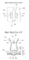
- FIG. 2 is a partial cross-sectional view of the structure of FIG. 1 , taken along the line and in the direction indicated by arrows J.
- the circuit board 204 includes a board body 222 having a mounting surface 222A; an interconnection pattern 223 provided on a surface 222B of the board body 222 on the opposite side from the mounting surface 222A; and a solder resist layer 224 having an opening 224A that exposes part of the interconnection pattern 223 that corresponds to a region where solder 226 is formed.
- the electronic components 205 are mounted on the mounting surface 222A of the board body 222.
- the electronic components 205 are electrically connected to the interconnection pattern 223.
- Examples of the electronic components 205 include a capacitor, a transformer, and a switching device.
- connection terminals 207 are provided in part of the peripheral part of the circuit board 204 which part faces the power supply plug 201.
- the connection terminals 207 are provided at such positions as to allow the connection terminals 207 to hold the connection parts 216 of the corresponding pin plugs 212.
- Each of the connection terminals 207 includes a fixing part 231 and a pair of elastically deformable pieces 233.
- the fixing part 231 includes a support part 235 that supports the elastically deformable pieces 233, and an electrical connection part 236 that penetrates through the board body 222 and the interconnection pattern 223.
- the electrical connection part 236 is fixed to the interconnection pattern 223 with the solder 226. Thereby, the connection terminals 207 are electrically connected to the circuit board 204.
- FIG. 3 is a cross-sectional view schematically illustrating the connection terminal 207 holding the connection part 216 of the corresponding pin plug 212.
- FIG. 4 is a diagram illustrating the structure illustrated in FIG. 3 viewed in the direction indicated by arrow K.
- the same elements as those of the structure illustrated in FIG. 2 are referred to by the same numerals.
- the elastically deformable pieces 233 are provided on the support part 235 so as to face each other.
- the elastically deformable pieces 233 include respective contact parts 238 that project toward the center of the elastically deformable pieces 233.
- the contact parts 238 electrically connect the circuit board 204 and the pin plug 212 by holding the connection part 216 of the pin plug 212 inserted in the connection terminal 207.
- the DC cord 208 has one end connected to the circuit board 204. Thereby, the DC cord 208 is electrically connected to the electronic components 205, the connection terminals 207, and the circuit board 204.
- the DC cord 208 has, at the other end, a plug 241 to be connected to an electronic apparatus (not graphically illustrated).
- the AC adapter 200 configured as described above converts alternating current (AC) power into direct current (DC) power, and supplies the DC power to the electronic apparatus (not graphically illustrated). (See, for example, Japanese Laid-Open Patent Application No. 11-224717 .)
- connection terminal and an AC adapter that can increase the reliability of the electrical connection between a terminal and a connection terminal by ensuring the holding of the terminal inserted in the connection terminal.
- a connection terminal to electrically connect to a terminal by holding the terminal includes a frame body including a first support part and a second support part positioned to face each other; and a third support part having a first end and a second end connected to an end of the first support part and an end of the second support part, respectively; a plurality of first elastic contact pieces provided on the first support part on a first side from which the terminal is to be inserted and having respective first contact parts configured to contact a peripheral surface of the terminal; a plurality of second elastic contact pieces provided on the second support part on the first side and having respective second contact parts configured to contact the peripheral surface of the terminal, the second contact parts being positioned to face the first contact parts; and a third elastic contact piece provided on the frame body on a second side opposite to the first side and configured to contact an end portion of the terminal.
- an AC adapter includes the connection terminal as set forth above; a circuit board having an interconnection pattern; an electronic component mounted on the circuit board; a power supply plug including a first case and a pin plug penetrating through the first case, the first case being attached to the circuit board; and a second case attached to the power supply plug, the second case including a housing part configured to house the circuit board having the electronic component mounted thereon, wherein the connection terminal is provided on the circuit board so that the pin plug faces the third elastic contact piece and is electrically connected to the interconnection pattern, and the connection terminal holds the pin plug so that the first contact parts, the second contact parts, and the third elastic contact piece are in contact with the end portion of the pin plug.
- FIG. 5 is a diagram for illustrating a problem of the conventional connection terminal.
- connection terminal 207 if a force greater than or equal to a certain value is applied to the elastically deformable pieces 233, the elastically deformable pieces 233 remain deformed (spread outward).
- connection failure is caused between the connection part 216 of the pin plug 212 and the elastically deformable pieces 233, thus causing the problem of reduction in the reliability of the electrical connection between the connection terminal 207 and the pin plug 212.
- connection terminal and an AC adapter are provided that can increase the reliability of the electrical connection between a terminal and a connection terminal by ensuring the holding of the terminal inserted in the connection terminal.
- FIG. 6 is an exploded plan view of an AC adapter according to the embodiment of the present invention.
- an AC adapter 10 includes a power supply plug 11, an upper case 12, a circuit board 14, electronic components 15, connection terminals 17, and a DC cord 18.
- the power supply plug 11 includes a lower case 21 and pin plugs 22, which are terminals.
- the lower case 21 has an attachment groove part (not graphically illustrated) for attachment of the circuit board 14.
- Each of the pin plugs 22 has a rod shape, and has an outlet insertion part 25 at one end and a connection part 26 at the other end.
- the outlet insertion part 25, which is configured to be inserted into an outlet, is exposed outside the lower case 21.
- the connection part 26, which is configured to be held by the corresponding connection terminal 17, projects from the interior wall of the lower case 21.
- the upper case 12 includes a housing part 28 for housing the circuit board 14 on which the electronic components 15 and the connection terminals 17 are mounted.
- the upper case 12 further includes a pair of guides 29 configured to guide the circuit board 14.
- FIG. 7 is a schematic partial cross-sectional view of the structure of FIG. 6 , taken along the line and in the direction indicated by arrows A.
- FIG. 8 is a partial cross-sectional view of the structure of FIG. 6 , taken along the line and in the direction indicated by arrows B.
- FIGS. 7 and 8 the same elements as those of the AC adapter 10 of this embodiment illustrated in FIG. 6 are referred to by the same numerals.
- FIG. 7 schematically illustrates the connection terminal 17 in the state of holding the connection part 26 of the corresponding pin plug 22.
- the circuit board 14 includes a board body 32, interconnection patterns 34, and a solder resist layer 35.
- the board body 32 is a plate-shaped substrate.
- the board body 32 has a mounting surface 32A, on which the electronic components 15 and the connection terminals 17 are mounted, and a surface 32B positioned on the opposite side (facing away) from the mounting surface 32A.
- Examples of the board body 32 include a phenolic substrate, a paper epoxy substrate, and a glass epoxy substrate.
- the interconnection patterns 34 are formed on the surface 32B of the board body 32.
- the solder resist layer 35 is formed on the surface 32B of the board body 32.
- the solder resist layer 35 has openings 35A that expose parts of the interconnection patterns 34 that correspond to regions where solder 36 is formed.
- the electronic component 15 includes an electronic component body 38 and pin terminals 39.
- the electronic component body 38 is placed on the mounting surface 32A of the board body 32.
- the pin terminals 39 are provided at the lower end of the electronic component body 38.
- the pin terminals 39 are electrically connected to the electronic component body 38.
- the pin terminals 39 penetrate through the board body 32 and the interconnection patterns 34. Portions of the pin terminals 39 projecting from the interconnection patterns 34 are fixed to the circuit board 14 with the solder 36 provided on the parts of the interconnection patterns 34 exposed in openings 35A.
- Examples of the electronic components 15 include a capacitor, a transformer, and a switching device.
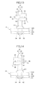
- FIG. 9 is a diagram illustrating the connection terminal 17 viewed in the direction indicated by arrow C in FIG. 6 .
- the same elements as those of the AC adapter 10 illustrated in FIG. 6 are referred to by the same numerals.
- FIG. 9 schematically illustrates the connection terminal 17 in the state of holding the connection part 26 of the corresponding pin plug 22.
- connection terminals 17 are provided on the mounting surface 32A of the board body 32 in part of the peripheral part of the circuit board 14.
- the connection terminals 17 are provided at such positions as to allow the connection terminals 17 to hold the connection parts 26 of the corresponding pin plugs 22.
- connection terminals 17 includes a frame body 41, a pair of first elastic contact pieces 43 and 44, a pair of second elastic contact pieces 45 and 46, and a third elastic contact piece 48.
- the elastic contact pieces forming part 55 is positioned on the mounting surface 32A of the board body 32. That is, the elastic contact pieces forming part 55 extends upward from the mounting surface 32A of the board body 32.
- the first elastic contact pieces 43 and 44 are connected to the elastic contact pieces forming part 55.
- One end of the elastic contact pieces forming part 55 (one end of the first support part 51) is connected to one end (a first end) of the third support part 53.
- the elastic contact pieces forming part 55 is formed as a unit with the third support part 53.
- the angle formed between the elastic contact pieces forming part 55 and the third support part 53 may be, for example, 90 degrees.
- the insertion part 56 is provided at the other end of the elastic contact pieces forming part 55.
- the insertion part 56 penetrates through the board body 32 and the corresponding interconnection pattern 34.
- a portion of the insertion part 56 projecting from the interconnection pattern 34 is bent so as to prevent the connection terminal 17 from coming off the circuit board 14.
- the portion of the insertion part 56 projecting from the interconnection pattern 34 is fixed to the interconnection pattern 34 with the solder 36.
- FIG. 10 is a diagram illustrating the connection terminal 17 viewed in the direction indicated by arrow D in FIG. 6 .
- the same elements as those of the AC adapter 10 illustrated in FIG. 6 are referred to by the same numerals.
- FIG. 10 schematically illustrates the connection terminal 17 in the state of holding the connection part 26 of the corresponding pin plug 22.
- the second support part 52 has a plate shape, and is positioned on the circuit board 14 to face the first support part 51.
- the second support part 52 includes an elastic contact pieces forming part 61, an insertion part 62, and a pair of projecting parts 63.
- the elastic contact pieces forming part 61 is formed as a unit with the third support part 53.
- the angle formed between the elastic contact pieces forming part 61 and the third support part 53 may be, for example, 90 degrees.
- the insertion part 62 is provided at the other end of the elastic contact pieces forming part 61.
- the insertion part 62 penetrates through the board body 32 and the corresponding interconnection pattern 34.
- a portion of the insertion part 62 projecting from the interconnection pattern 34 is bent so as to prevent the connection terminal 17 from coming off the circuit board 14.
- the portion of the insertion part 62 projecting from the interconnection pattern 34 is fixed to the interconnection pattern 34 with the solder 36.
- the projecting parts 63 are provided on portions of the elastic contact pieces forming part 61 near the insertion part 62.
- the projecting parts 63 prevent the insertion of the elastic contact pieces forming part 61 into the board body 32.
- the third support part 53 connecting the end of the elastic contact pieces forming part 55 on the side opposite from the side on which the elastic contact pieces forming part 55 is mounted on the circuit board 14 and the end of the elastic contact pieces forming part 61 on the side opposite from the side on which the elastic contact pieces forming part 61 is mounted on the circuit board 14, the interval between the elastic contact pieces forming part 55 where the first elastic contact pieces 43 and 44 are formed and the elastic contact pieces forming part 61 where the second elastic contact pieces 45 and 46 are formed is prevented from widening. Therefore, it is possible to hold the peripheral surface of the connection part 26 of the pin plug 22 tightly between the first elastic contact pieces 43 and 44 and the second elastic contact pieces 45 and 46.
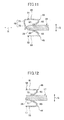
- the third elastic contact piece 48 has a spring characteristic so as to be displaceable in the directions indicated by H in FIG. 11 (directions perpendicular to the directions indicated by G in FIG. 11 ).
- the third elastic contact piece 48 includes a support part 74 and a contact part 75.
Landscapes
- Coupling Device And Connection With Printed Circuit (AREA)
- Connecting Device With Holders (AREA)
- Connector Housings Or Holding Contact Members (AREA)
Applications Claiming Priority (1)
| Application Number | Priority Date | Filing Date | Title |
|---|---|---|---|
| JP2009206710A JP5509744B2 (ja) | 2009-09-08 | 2009-09-08 | 接続端子及びacアダプタ |
Publications (3)
| Publication Number | Publication Date |
|---|---|
| EP2293394A2 true EP2293394A2 (de) | 2011-03-09 |
| EP2293394A3 EP2293394A3 (de) | 2014-05-21 |
| EP2293394B1 EP2293394B1 (de) | 2017-05-17 |
Family
ID=43217230
Family Applications (1)
| Application Number | Title | Priority Date | Filing Date |
|---|---|---|---|
| EP10175540.3A Not-in-force EP2293394B1 (de) | 2009-09-08 | 2010-09-07 | Verbindungsendgerät und Wechselstromadapter |
Country Status (4)
| Country | Link |
|---|---|
| US (1) | US8391019B2 (de) |
| EP (1) | EP2293394B1 (de) |
| JP (1) | JP5509744B2 (de) |
| CN (1) | CN102013592B (de) |
Families Citing this family (2)
| Publication number | Priority date | Publication date | Assignee | Title |
|---|---|---|---|---|
| TWI799043B (zh) * | 2021-12-29 | 2023-04-11 | 飛宏科技股份有限公司 | 電源插頭裝置 |
| WO2025237360A1 (zh) * | 2024-05-15 | 2025-11-20 | 嘉兴山蒲照明电器有限公司 | Led灯具及其装配方法 |
Citations (1)
| Publication number | Priority date | Publication date | Assignee | Title |
|---|---|---|---|---|
| JPH11224717A (ja) | 1998-02-04 | 1999-08-17 | Mitsumi Electric Co Ltd | Acアダプタ |
Family Cites Families (7)
| Publication number | Priority date | Publication date | Assignee | Title |
|---|---|---|---|---|
| JPS59152670U (ja) * | 1983-03-31 | 1984-10-13 | 松下電工株式会社 | 基板用コネクタ |
| GB9411809D0 (en) * | 1994-06-13 | 1994-08-03 | Amp Gmbh | Electrical receptacle terminal |
| FR2783098B1 (fr) * | 1998-09-08 | 2000-10-06 | Cinch Connecteurs Sa | Organe de contact electrique femelle |
| JP2001093608A (ja) * | 1999-09-22 | 2001-04-06 | Omron Corp | 電気コンタクト及び電気コンタクトユニット |
| US6644984B2 (en) * | 2002-02-08 | 2003-11-11 | Astec International Limited | Plug assembly with spring loaded contact terminals |
| DE102006009074B4 (de) * | 2006-02-28 | 2016-02-25 | Robert Bosch Gmbh | Elektrischer Steckverbinder mit vorgespannter Kontaktlamelle |
| JP5130948B2 (ja) * | 2008-02-19 | 2013-01-30 | ミツミ電機株式会社 | Acアダプタ及びその組付け方法 |
-
2009
- 2009-09-08 JP JP2009206710A patent/JP5509744B2/ja active Active
-
2010
- 2010-09-03 US US12/875,275 patent/US8391019B2/en not_active Expired - Fee Related
- 2010-09-06 CN CN201010274726.6A patent/CN102013592B/zh not_active Expired - Fee Related
- 2010-09-07 EP EP10175540.3A patent/EP2293394B1/de not_active Not-in-force
Patent Citations (1)
| Publication number | Priority date | Publication date | Assignee | Title |
|---|---|---|---|---|
| JPH11224717A (ja) | 1998-02-04 | 1999-08-17 | Mitsumi Electric Co Ltd | Acアダプタ |
Also Published As
| Publication number | Publication date |
|---|---|
| CN102013592B (zh) | 2015-03-25 |
| EP2293394B1 (de) | 2017-05-17 |
| US20110058345A1 (en) | 2011-03-10 |
| CN102013592A (zh) | 2011-04-13 |
| JP5509744B2 (ja) | 2014-06-04 |
| JP2011060480A (ja) | 2011-03-24 |
| US8391019B2 (en) | 2013-03-05 |
| EP2293394A3 (de) | 2014-05-21 |
Similar Documents
| Publication | Publication Date | Title |
|---|---|---|
| TW457752B (en) | Device-to-board electrical connector | |
| US8556640B2 (en) | Electrical connector | |
| US7815474B1 (en) | Probe connector having a mounting platform | |
| US8721350B2 (en) | Electrical connector and electrical connector assembly | |
| US9812801B2 (en) | Cable holding member, plug connector, connector device, flat cable, and method for assembling plug connector | |
| US20110318944A1 (en) | Probe Connector | |
| JP2016146255A (ja) | ソケット型コネクタ及びコネクタユニット | |
| KR20180046886A (ko) | 기판용 커넥터 | |
| US6960094B2 (en) | Flat and thin connector for electrically connecting a flexible printed circuit board and a hard board | |
| JP4756716B2 (ja) | コネクタ及び電子装置 | |
| EP2293394B1 (de) | Verbindungsendgerät und Wechselstromadapter | |
| JP2008059810A (ja) | コネクタ | |
| EP2031710A1 (de) | Buchse zur montage eines elektronischen bauteils | |
| CN102656752B (zh) | 连接器的固定结构 | |
| US11114787B2 (en) | Terminal for connector mounted to printed circuit board and connector supporting said terminal | |
| JP6239582B2 (ja) | 電気コネクタ | |
| JP2007042384A (ja) | 電気コネクタ | |
| WO2011074697A1 (en) | Fixing structure for connector | |
| KR101002932B1 (ko) | 전기 커넥터 | |
| KR20090046524A (ko) | 박막형 커넥터 | |
| KR100502700B1 (ko) | 전기 콘넥터 | |
| US7708568B1 (en) | Connector assembly | |
| JP2005150052A (ja) | 電子部品取付用ソケット | |
| JP2005129276A (ja) | 接続装置 | |
| KR200324360Y1 (ko) | 전기 콘넥터 |
Legal Events
| Date | Code | Title | Description |
|---|---|---|---|
| PUAI | Public reference made under article 153(3) epc to a published international application that has entered the european phase |
Free format text: ORIGINAL CODE: 0009012 |
|
| AK | Designated contracting states |
Kind code of ref document: A2 Designated state(s): AL AT BE BG CH CY CZ DE DK EE ES FI FR GB GR HR HU IE IS IT LI LT LU LV MC MK MT NL NO PL PT RO SE SI SK SM TR |
|
| AX | Request for extension of the european patent |
Extension state: BA ME RS |
|
| PUAL | Search report despatched |
Free format text: ORIGINAL CODE: 0009013 |
|
| AK | Designated contracting states |
Kind code of ref document: A3 Designated state(s): AL AT BE BG CH CY CZ DE DK EE ES FI FR GB GR HR HU IE IS IT LI LT LU LV MC MK MT NL NO PL PT RO SE SI SK SM TR |
|
| AX | Request for extension of the european patent |
Extension state: BA ME RS |
|
| RIC1 | Information provided on ipc code assigned before grant |
Ipc: H01R 13/66 20060101ALI20140414BHEP Ipc: H01R 31/06 20060101AFI20140414BHEP Ipc: H01R 13/24 20060101ALI20140414BHEP Ipc: H01R 13/11 20060101ALI20140414BHEP |
|
| 17P | Request for examination filed |
Effective date: 20140930 |
|
| RBV | Designated contracting states (corrected) |
Designated state(s): AL AT BE BG CH CY CZ DE DK EE ES FI FR GB GR HR HU IE IS IT LI LT LU LV MC MK MT NL NO PL PT RO SE SI SK SM TR |
|
| GRAP | Despatch of communication of intention to grant a patent |
Free format text: ORIGINAL CODE: EPIDOSNIGR1 |
|
| INTG | Intention to grant announced |
Effective date: 20161212 |
|
| RIN1 | Information on inventor provided before grant (corrected) |
Inventor name: MASATOSHI, KURODA Inventor name: HIROTAKA, YAMAMOTO Inventor name: TORU, YOSHINO Inventor name: EIJI, YOSHIDA |
|
| GRAS | Grant fee paid |
Free format text: ORIGINAL CODE: EPIDOSNIGR3 |
|
| GRAA | (expected) grant |
Free format text: ORIGINAL CODE: 0009210 |
|
| AK | Designated contracting states |
Kind code of ref document: B1 Designated state(s): AL AT BE BG CH CY CZ DE DK EE ES FI FR GB GR HR HU IE IS IT LI LT LU LV MC MK MT NL NO PL PT RO SE SI SK SM TR |
|
| REG | Reference to a national code |
Ref country code: GB Ref legal event code: FG4D |
|
| RIN1 | Information on inventor provided before grant (corrected) |
Inventor name: HIROTAKA, YAMAMOTO Inventor name: TORU, YOSHINO Inventor name: EIJI, YOSHIDA Inventor name: MASATOSHI, KURODA |
|
| REG | Reference to a national code |
Ref country code: CH Ref legal event code: EP |
|
| REG | Reference to a national code |
Ref country code: IE Ref legal event code: FG4D |
|
| REG | Reference to a national code |
Ref country code: AT Ref legal event code: REF Ref document number: 895240 Country of ref document: AT Kind code of ref document: T Effective date: 20170615 |
|
| REG | Reference to a national code |
Ref country code: DE Ref legal event code: R096 Ref document number: 602010042377 Country of ref document: DE |
|
| REG | Reference to a national code |
Ref country code: NL Ref legal event code: MP Effective date: 20170517 |
|
| REG | Reference to a national code |
Ref country code: LT Ref legal event code: MG4D |
|
| REG | Reference to a national code |
Ref country code: AT Ref legal event code: MK05 Ref document number: 895240 Country of ref document: AT Kind code of ref document: T Effective date: 20170517 |
|
| PG25 | Lapsed in a contracting state [announced via postgrant information from national office to epo] |
Ref country code: HR Free format text: LAPSE BECAUSE OF FAILURE TO SUBMIT A TRANSLATION OF THE DESCRIPTION OR TO PAY THE FEE WITHIN THE PRESCRIBED TIME-LIMIT Effective date: 20170517 Ref country code: ES Free format text: LAPSE BECAUSE OF FAILURE TO SUBMIT A TRANSLATION OF THE DESCRIPTION OR TO PAY THE FEE WITHIN THE PRESCRIBED TIME-LIMIT Effective date: 20170517 Ref country code: FI Free format text: LAPSE BECAUSE OF FAILURE TO SUBMIT A TRANSLATION OF THE DESCRIPTION OR TO PAY THE FEE WITHIN THE PRESCRIBED TIME-LIMIT Effective date: 20170517 Ref country code: GR Free format text: LAPSE BECAUSE OF FAILURE TO SUBMIT A TRANSLATION OF THE DESCRIPTION OR TO PAY THE FEE WITHIN THE PRESCRIBED TIME-LIMIT Effective date: 20170818 Ref country code: LT Free format text: LAPSE BECAUSE OF FAILURE TO SUBMIT A TRANSLATION OF THE DESCRIPTION OR TO PAY THE FEE WITHIN THE PRESCRIBED TIME-LIMIT Effective date: 20170517 Ref country code: AT Free format text: LAPSE BECAUSE OF FAILURE TO SUBMIT A TRANSLATION OF THE DESCRIPTION OR TO PAY THE FEE WITHIN THE PRESCRIBED TIME-LIMIT Effective date: 20170517 Ref country code: NO Free format text: LAPSE BECAUSE OF FAILURE TO SUBMIT A TRANSLATION OF THE DESCRIPTION OR TO PAY THE FEE WITHIN THE PRESCRIBED TIME-LIMIT Effective date: 20170817 |
|
| PG25 | Lapsed in a contracting state [announced via postgrant information from national office to epo] |
Ref country code: SE Free format text: LAPSE BECAUSE OF FAILURE TO SUBMIT A TRANSLATION OF THE DESCRIPTION OR TO PAY THE FEE WITHIN THE PRESCRIBED TIME-LIMIT Effective date: 20170517 Ref country code: BG Free format text: LAPSE BECAUSE OF FAILURE TO SUBMIT A TRANSLATION OF THE DESCRIPTION OR TO PAY THE FEE WITHIN THE PRESCRIBED TIME-LIMIT Effective date: 20170817 Ref country code: LV Free format text: LAPSE BECAUSE OF FAILURE TO SUBMIT A TRANSLATION OF THE DESCRIPTION OR TO PAY THE FEE WITHIN THE PRESCRIBED TIME-LIMIT Effective date: 20170517 Ref country code: PL Free format text: LAPSE BECAUSE OF FAILURE TO SUBMIT A TRANSLATION OF THE DESCRIPTION OR TO PAY THE FEE WITHIN THE PRESCRIBED TIME-LIMIT Effective date: 20170517 Ref country code: NL Free format text: LAPSE BECAUSE OF FAILURE TO SUBMIT A TRANSLATION OF THE DESCRIPTION OR TO PAY THE FEE WITHIN THE PRESCRIBED TIME-LIMIT Effective date: 20170517 Ref country code: IS Free format text: LAPSE BECAUSE OF FAILURE TO SUBMIT A TRANSLATION OF THE DESCRIPTION OR TO PAY THE FEE WITHIN THE PRESCRIBED TIME-LIMIT Effective date: 20170917 |
|
| PG25 | Lapsed in a contracting state [announced via postgrant information from national office to epo] |
Ref country code: SK Free format text: LAPSE BECAUSE OF FAILURE TO SUBMIT A TRANSLATION OF THE DESCRIPTION OR TO PAY THE FEE WITHIN THE PRESCRIBED TIME-LIMIT Effective date: 20170517 Ref country code: DK Free format text: LAPSE BECAUSE OF FAILURE TO SUBMIT A TRANSLATION OF THE DESCRIPTION OR TO PAY THE FEE WITHIN THE PRESCRIBED TIME-LIMIT Effective date: 20170517 Ref country code: RO Free format text: LAPSE BECAUSE OF FAILURE TO SUBMIT A TRANSLATION OF THE DESCRIPTION OR TO PAY THE FEE WITHIN THE PRESCRIBED TIME-LIMIT Effective date: 20170517 Ref country code: CZ Free format text: LAPSE BECAUSE OF FAILURE TO SUBMIT A TRANSLATION OF THE DESCRIPTION OR TO PAY THE FEE WITHIN THE PRESCRIBED TIME-LIMIT Effective date: 20170517 Ref country code: EE Free format text: LAPSE BECAUSE OF FAILURE TO SUBMIT A TRANSLATION OF THE DESCRIPTION OR TO PAY THE FEE WITHIN THE PRESCRIBED TIME-LIMIT Effective date: 20170517 |
|
| REG | Reference to a national code |
Ref country code: DE Ref legal event code: R097 Ref document number: 602010042377 Country of ref document: DE |
|
| PG25 | Lapsed in a contracting state [announced via postgrant information from national office to epo] |
Ref country code: IT Free format text: LAPSE BECAUSE OF FAILURE TO SUBMIT A TRANSLATION OF THE DESCRIPTION OR TO PAY THE FEE WITHIN THE PRESCRIBED TIME-LIMIT Effective date: 20170517 Ref country code: SM Free format text: LAPSE BECAUSE OF FAILURE TO SUBMIT A TRANSLATION OF THE DESCRIPTION OR TO PAY THE FEE WITHIN THE PRESCRIBED TIME-LIMIT Effective date: 20170517 |
|
| PLBE | No opposition filed within time limit |
Free format text: ORIGINAL CODE: 0009261 |
|
| STAA | Information on the status of an ep patent application or granted ep patent |
Free format text: STATUS: NO OPPOSITION FILED WITHIN TIME LIMIT |
|
| REG | Reference to a national code |
Ref country code: DE Ref legal event code: R119 Ref document number: 602010042377 Country of ref document: DE |
|
| 26N | No opposition filed |
Effective date: 20180220 |
|
| REG | Reference to a national code |
Ref country code: CH Ref legal event code: PL |
|
| PG25 | Lapsed in a contracting state [announced via postgrant information from national office to epo] |
Ref country code: MC Free format text: LAPSE BECAUSE OF FAILURE TO SUBMIT A TRANSLATION OF THE DESCRIPTION OR TO PAY THE FEE WITHIN THE PRESCRIBED TIME-LIMIT Effective date: 20170517 Ref country code: SI Free format text: LAPSE BECAUSE OF FAILURE TO SUBMIT A TRANSLATION OF THE DESCRIPTION OR TO PAY THE FEE WITHIN THE PRESCRIBED TIME-LIMIT Effective date: 20170517 |
|
| REG | Reference to a national code |
Ref country code: IE Ref legal event code: MM4A |
|
| REG | Reference to a national code |
Ref country code: BE Ref legal event code: MM Effective date: 20170930 |
|
| PG25 | Lapsed in a contracting state [announced via postgrant information from national office to epo] |
Ref country code: LU Free format text: LAPSE BECAUSE OF NON-PAYMENT OF DUE FEES Effective date: 20170907 |
|
| REG | Reference to a national code |
Ref country code: FR Ref legal event code: ST Effective date: 20180531 |
|
| PG25 | Lapsed in a contracting state [announced via postgrant information from national office to epo] |
Ref country code: DE Free format text: LAPSE BECAUSE OF NON-PAYMENT OF DUE FEES Effective date: 20180404 Ref country code: IE Free format text: LAPSE BECAUSE OF NON-PAYMENT OF DUE FEES Effective date: 20170907 Ref country code: LI Free format text: LAPSE BECAUSE OF NON-PAYMENT OF DUE FEES Effective date: 20170930 Ref country code: CH Free format text: LAPSE BECAUSE OF NON-PAYMENT OF DUE FEES Effective date: 20170930 |
|
| PG25 | Lapsed in a contracting state [announced via postgrant information from national office to epo] |
Ref country code: FR Free format text: LAPSE BECAUSE OF NON-PAYMENT OF DUE FEES Effective date: 20171002 Ref country code: BE Free format text: LAPSE BECAUSE OF NON-PAYMENT OF DUE FEES Effective date: 20170930 |
|
| PG25 | Lapsed in a contracting state [announced via postgrant information from national office to epo] |
Ref country code: MT Free format text: LAPSE BECAUSE OF NON-PAYMENT OF DUE FEES Effective date: 20170907 |
|
| PG25 | Lapsed in a contracting state [announced via postgrant information from national office to epo] |
Ref country code: HU Free format text: LAPSE BECAUSE OF FAILURE TO SUBMIT A TRANSLATION OF THE DESCRIPTION OR TO PAY THE FEE WITHIN THE PRESCRIBED TIME-LIMIT; INVALID AB INITIO Effective date: 20100907 |
|
| PG25 | Lapsed in a contracting state [announced via postgrant information from national office to epo] |
Ref country code: CY Free format text: LAPSE BECAUSE OF NON-PAYMENT OF DUE FEES Effective date: 20170517 |
|
| PG25 | Lapsed in a contracting state [announced via postgrant information from national office to epo] |
Ref country code: MK Free format text: LAPSE BECAUSE OF FAILURE TO SUBMIT A TRANSLATION OF THE DESCRIPTION OR TO PAY THE FEE WITHIN THE PRESCRIBED TIME-LIMIT Effective date: 20170517 |
|
| PGFP | Annual fee paid to national office [announced via postgrant information from national office to epo] |
Ref country code: GB Payment date: 20190905 Year of fee payment: 10 |
|
| PG25 | Lapsed in a contracting state [announced via postgrant information from national office to epo] |
Ref country code: TR Free format text: LAPSE BECAUSE OF FAILURE TO SUBMIT A TRANSLATION OF THE DESCRIPTION OR TO PAY THE FEE WITHIN THE PRESCRIBED TIME-LIMIT Effective date: 20170517 |
|
| PG25 | Lapsed in a contracting state [announced via postgrant information from national office to epo] |
Ref country code: PT Free format text: LAPSE BECAUSE OF FAILURE TO SUBMIT A TRANSLATION OF THE DESCRIPTION OR TO PAY THE FEE WITHIN THE PRESCRIBED TIME-LIMIT Effective date: 20170517 |
|
| PG25 | Lapsed in a contracting state [announced via postgrant information from national office to epo] |
Ref country code: AL Free format text: LAPSE BECAUSE OF FAILURE TO SUBMIT A TRANSLATION OF THE DESCRIPTION OR TO PAY THE FEE WITHIN THE PRESCRIBED TIME-LIMIT Effective date: 20170517 |
|
| GBPC | Gb: european patent ceased through non-payment of renewal fee |
Effective date: 20200907 |
|
| PG25 | Lapsed in a contracting state [announced via postgrant information from national office to epo] |
Ref country code: GB Free format text: LAPSE BECAUSE OF NON-PAYMENT OF DUE FEES Effective date: 20200907 |