EP2293344A1 - Solarzelle und herstellungsverfahren dafür - Google Patents
Solarzelle und herstellungsverfahren dafür Download PDFInfo
- Publication number
- EP2293344A1 EP2293344A1 EP09766585A EP09766585A EP2293344A1 EP 2293344 A1 EP2293344 A1 EP 2293344A1 EP 09766585 A EP09766585 A EP 09766585A EP 09766585 A EP09766585 A EP 09766585A EP 2293344 A1 EP2293344 A1 EP 2293344A1
- Authority
- EP
- European Patent Office
- Prior art keywords
- electrode
- film
- solar cell
- photoelectric conversion
- alloy
- Prior art date
- Legal status (The legal status is an assumption and is not a legal conclusion. Google has not performed a legal analysis and makes no representation as to the accuracy of the status listed.)
- Withdrawn
Links
Images

Classifications
-
- H—ELECTRICITY
- H10—SEMICONDUCTOR DEVICES; ELECTRIC SOLID-STATE DEVICES NOT OTHERWISE PROVIDED FOR
- H10F—INORGANIC SEMICONDUCTOR DEVICES SENSITIVE TO INFRARED RADIATION, LIGHT, ELECTROMAGNETIC RADIATION OF SHORTER WAVELENGTH OR CORPUSCULAR RADIATION
- H10F77/00—Constructional details of devices covered by this subclass
- H10F77/20—Electrodes
- H10F77/206—Electrodes for devices having potential barriers
- H10F77/211—Electrodes for devices having potential barriers for photovoltaic cells
-
- H—ELECTRICITY
- H10—SEMICONDUCTOR DEVICES; ELECTRIC SOLID-STATE DEVICES NOT OTHERWISE PROVIDED FOR
- H10F—INORGANIC SEMICONDUCTOR DEVICES SENSITIVE TO INFRARED RADIATION, LIGHT, ELECTROMAGNETIC RADIATION OF SHORTER WAVELENGTH OR CORPUSCULAR RADIATION
- H10F77/00—Constructional details of devices covered by this subclass
- H10F77/40—Optical elements or arrangements
- H10F77/42—Optical elements or arrangements directly associated or integrated with photovoltaic cells, e.g. light-reflecting means or light-concentrating means
- H10F77/48—Back surface reflectors [BSR]
-
- Y—GENERAL TAGGING OF NEW TECHNOLOGICAL DEVELOPMENTS; GENERAL TAGGING OF CROSS-SECTIONAL TECHNOLOGIES SPANNING OVER SEVERAL SECTIONS OF THE IPC; TECHNICAL SUBJECTS COVERED BY FORMER USPC CROSS-REFERENCE ART COLLECTIONS [XRACs] AND DIGESTS
- Y02—TECHNOLOGIES OR APPLICATIONS FOR MITIGATION OR ADAPTATION AGAINST CLIMATE CHANGE
- Y02E—REDUCTION OF GREENHOUSE GAS [GHG] EMISSIONS, RELATED TO ENERGY GENERATION, TRANSMISSION OR DISTRIBUTION
- Y02E10/00—Energy generation through renewable energy sources
- Y02E10/50—Photovoltaic [PV] energy
- Y02E10/52—PV systems with concentrators
Definitions
- the present invention relates to a solar cell having an alloy electrode and a method of manufacturing the solar cell.
- Priority is claimed based on Japanese Patent Application No. 2008-157713, filed June 17, 2008 , the content of which is incorporated herein by reference.
- solar cells have been widely used as photoelectric conversion devices.
- this type of solar cell there are crystalline silicon solar cells in which single-crystalline silicon or polysilicon is used as a semiconductor layer (photoelectric conversion layer) and thin film silicon solar cells in which amorphous silicon and/or microcrystal silicon are used as a semiconductor layer.
- Conventional thin film silicon solar cells have a configuration in which, for example, on a glass substrate, an electrode having transparency (transparent electrode) is formed as a first electrode (surface transparent electrode); a semiconductor layer (photoelectric conversion layer) of silicon (amorphous silicon and/or microcrystal silicon) and a light transmissive buffer layer are sequentially formed on the first electrode; a pure metal electrode having reflectivity (repeller) is formed as a second electrode (back surface metal electrode) on the buffer layer; and a protective layer is formed on the second electrode (for example, see Patent Document 1).
- the above-mentioned silicon photoelectric conversion layer has a p-i-n junction structure or n-i-p junction structure in which an i-type silicon film, which is excited by incident light and mainly generates electrons and holes, is sandwiched between p-type and n-type silicon films.
- a tandem structure has become known in which an amorphous silicon photoelectric conversion layer and a microcrystal silicon photoelectric conversion layer are laminated to improve a conversion rate.
- the sunlight entering a glass substrate passes through the surface transparent electrode and then enters the photoelectric conversion layer.
- energy particles referred to as photons which are included in the sunlight
- hit the i-type silicon electrons and holes are generated by a photovoltaic effect.
- the electrons move toward the n-type silicon and the holes move toward the p-type silicon.
- the light energy can be converted into the electric energy.
- the light transmitted through the photoelectric conversion layer is reflected by the surface of the back surface metal electrode and then once again directed to the photoelectric conversion layer.
- electrons and holes are generated in the photoelectric conversion layer and the light energy is thus converted into the electric energy.
- a silver (Ag) electrode having low resistance and high optical reflectance is formed by sputtering.
- the buffer layer for example, an AZO (ZnO with A1 added thereto) film or a GZO (ZnO with Ga added thereto) film is formed.
- the buffer layer functions as a barrier layer between the photoelectric conversion layer and the back surface metal electrode.
- an Ag electrode which uses Ag as a material for the back surface metal electrode, is used.
- Ag electrode silver oxide is formed at the interface between the Ag electrode and the buffer layer as oxide, and thus optical reflectance is lowered. Accordingly, the light transmitted through the photoelectric conversion layer cannot be sufficiently reflected in some cases.
- the light intensity reflected by the Ag electrode and returning to the photoelectric conversion layer decreases, a problem occurs in that the incident photon-to-current conversion efficiency of the solar cell is lowered.
- holes are formed at the interface between the Ag electrode and the buffer layer in some cases.
- the conventional solar cell has a problem in that the reliability and fill factor of the solar cell are decreased by the Ag electrode as the second electrode.
- the present invention is contrived in view of the above-described circumstances and an object of the present invention is to provide a solar cell having improved incident photon-to-current conversion efficiency and reliability and a method of manufacturing the solar cell.
- the present invention employed the following measures to solve the above-mentioned problems and to achieve the object. That is,
- a solar cell of the present invention As the material for a second electrode, an alloy including Ag as a main component with at least one of Sn and Au added thereto is used. In this manner, reflectance of the metal electrode can be improved and adhesion with a buffer layer can be improved. Accordingly, since an increase in contact resistance at the interface is suppressed and incident photon-to-current conversion Efficiency can thus be improved, the incident photon-to-current conversion efficiency and reliability of the solar cell can be improved (the adhesion is improved by adding Sn and reflection characteristics and corrosion resistance are improved by adding Au).
- FIG 1 is a partial cross-sectional diagram showing the configuration of a solar cell according to this embodiment.
- a solar cell 10 according to this embodiment includes a light transmissive substrate 11, a light transmissive first electrode (surface transparent electrode) 13, a silicon semiconductor layer (photoelectric conversion layer) 14, a light transmissive buffer layer 15, a second electrode (back surface alloy electrode) 16 and a protective layer 17.
- the first electrode 13, the photoelectric conversion layer 14, the buffer layer 15 and the second electrode 16 which are sequentially laminated on a side (back surface) 11a of the substrate 11, constitute a photoelectric conversion body 12.
- the substrate 11 is formed of an insulating material such as glass or a transparent resin which has durability and excellent permeability of sunlight.
- sunlight is incident from the opposite side of the photoelectric conversion body 12 with the substrate 11 interposed therebetween, that is, from the other side (surface) 11b of the substrate 11.
- the first electrode (surface electrode) 13 is formed of light transmissive metal oxide such as AZO (ZnO with A1 added thereto) or GZO (ZnO with Ga added thereto) or transparent conducting oxide (TCO) such as indium tin oxide (ITO), and is formed on the back surface 11a of the substrate 11.
- light transmissive metal oxide such as AZO (ZnO with A1 added thereto) or GZO (ZnO with Ga added thereto) or transparent conducting oxide (TCO) such as indium tin oxide (ITO)
- the silicon photoelectric conversion layer (semiconductor layer) 14 is formed on the first electrode 13.
- the photoelectric conversion layer 14 has a p-i-n junction structure or n-i-p junction structure in which an i-type silicon film (amorphous silicon film and/or microcrystal silicon) is sandwiched between a p-type silicon film (amorphous silicon film and/or microcrystal silicon) and an n-type silicon film (amorphous silicon film and/or microcrystal silicon).
- a p-type amorphous silicon film, an i-type amorphous silicon film and an n-type amorphous silicon film are sequentially laminated from the side of the surface transparent electrode 13.
- a p-i-n junction structure or n-i-p junction structure of microcrystal silicon may be laminated.
- the barrier layer 15 is formed of transparent conducting oxide (TCO) such as light transmissive metal oxide having low resistance (for example, AZO (ZnO with A1 added thereto) or GZO (Zn0 with Ga added thereto) having a film thickness of 40 to 100 nm), and is formed between the photoelectric conversion layer 14 and the second electrode 16.
- TCO transparent conducting oxide
- the buffer layer 15 functions as a barrier layer for preventing the silicon film of the photoelectric conversion layer 14 from being damaged by the formation of the second electrode 16 by sputtering and preventing silver (Ag), which is a constituent material of the second electrode 16, from being alloyed with the silicon.
- the buffer layer 15 is provided in the migration path of the holes in order to remove from the first electrode 13 the holes which are generated in the i-type silicon by photoelectric conversion. Accordingly, in order not to lower the incident photon-to-current conversion efficiency of the solar cell 10, it is preferable that the buffer layer 15 has conductive properties to preserve the electric conductivity between the photoelectric conversion layer 14 and the first electrode 16, and is formed of a material having low contact resistance.
- the buffer layer is a film that provides excellent coverage during film forming.
- the second electrode (back surface alloy electrode) 16 is an alloy electrode formed of a silver alloy including tin (Sn), gold (Au) and silver (Ag) and is formed on the buffer layer 15.
- the alloy electrode 16 is an alloy which includes Ag as a main component with Sn and Au added thereto and is formed at a film thickness of, for example, 200 to 250 nm by sputtering.
- the alloy electrode 16 functions as an electrode for taking out the holes generated in the photoelectric conversion layer 14.
- the alloy electrode 16 also has a function of reflecting the light which enters the photoelectric conversion layer 14 via the substrate 11 and the transparent electrode 13, and is transmitted through the photoelectric conversion layer 14 and the buffer layer 15, and returning the light to the photoelectric conversion layer 14 to contribute to the photoelectric conversion.
- the ASA (Ag-Sn-Au) film constituting the alloy electrode (second electrode) 16 is formed of 0.1 to 2.5 of Sn, 0.1 to 4.0 of Au and the balance Ag in terms of atom% units (at%).
- the content of Au By adjusting the content of Au to 0.1 to 4.0 at%, the reflectance on the long-wavelength side of the light entering the second electrode 16 can be remarkably improved over the case of a conventional Ag electrode and the corrosion resistance of the alloy electrode can be remarkably improved. This is because when the content of Au is less than 0.1 at%, the improvement in reflectance is not remarkable, and when the content of Au is greater than 4.0 at%, cost increases occur and, thus, the above-mentioned effects are offset.
- adhesion with the buffer layer 15 can be remarkably improved over the case of a conventional Ag electrode. This is because when the content of Sn is less than 0.1 at%, the improvement in the adhesion properties is not prominent, and when the content of Sn is greater than 2.5 at%, the resistance of the ASA film is increased.
- the substrate 11 is provided, and on the back surface 11a of the substrate 11, a TCO film is formed as the first electrode (surface transparent electrode) 13. Since a glass substrate with TCO is commercially available, it may be provided. However, an AZO film or a GZO film may be formed on a glass substrate by sputtering.
- a ZnO sintered object with A1 or Ga added thereto is used as a target, and a ZnO film is formed under reduced pressure with argon gas as a sputtering gas or under reduced pressure with argon gas with oxygen gas added thereto as a sputtering gas.
- a p-type silicon film, an i-type silicon film and an n-type silicon film constituting the photoelectric conversion layer 14 are laminated and formed by a CVD method.
- anAZO film or a GZO film constituting the buffer layer 15 is formed by sputtering.
- an ASA film is formed as the alloy electrode (second electrode) 16 by sputtering.
- a target silica target with 0.1 to 2.5 at% of Sn and 0.1 to 4.0 at% of Au added thereto
- the ASA film is formed under reduced pressure with argon gas as a sputtering gas.
- oxygen it is desirable to add oxygen to the sputtering gas. By adding oxygen only to the film-forming initial stage, adhesion with the GZO film is improved and an increase in contact resistance can be suppressed.
- the ASA film-forming sputtering an alloy film, which has almost the same composition as that of the target in metal components, can be formed. Accordingly, the ASA film formed becomes a silver alloy film with 0.1 to 2.5 at% of Sn and 0.1 to 4.0 at% of Au added thereto.
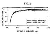
- FIG 2 is a graph showing the reflectance characteristics with respect to incident light wavelength in the ASA film constituting the second electrode 16 of the solar cell 10.
- the reflectance characteristics with respect to incident light wavelength in an Ag film constituting the second electrode of a conventional solar cell are also shown as a comparative example.
- an ASA film which is used in the present invention and an Ag film which is used in a conventional solar cell are formed at the same film thickness on a glass substrate, respectively.
- the wavelength of light contributing to the photoelectric conversion is in the range of 300 to 800 nm.
- the optical reflectance of the ASA film is higher than that in the conventional Ag film.
- the optical reflectance of the Ag film is in the range of 90% to 92% and the optical reflectance of the ASA film is in the range of 94% to 96%. Improvement in the optical wavelength on the long-wavelength side is obtained via the added Au. Accordingly, even when an Ag alloy film including Ag as a main component with Au added thereto and no addition of Sn is used, the above-mentioned improvement in optical reflectance obtained.
- the optical reflectance of the ASA film is the same as in the conventional Ag film. Accordingly, in the solar cell 10 according to this embodiment in which the second electrode 16 is constituted by the ASA alloy, while the optical reflectance at the short-wavelength side of the second electrode 16 is secured so as to be the same as the optical reflectance of the conventional Ag electrode, the optical reflectance at the long-wavelength side can be improved than the optical reflectance of the conventional Ag electrode.
- the solar cell mainly light beams on the short-wavelength side among light beams incident from the substrate are directly absorbed by the photoelectric conversion layer and contribute to the photoelectric conversion, and thus they do not reach the second electrode and the remaining light beams on the long-wavelength side are transmitted through the photoelectric conversion layer and the buffer layer and reach the second electrode. Accordingly, high optical reflection on the long-wavelength side of the second electrode 16 means that it is possible to efficiently return the light transmitted through the photoelectric conversion layer 14 to the photoelectric conversion layer 14 and the incident photon-to-current conversion Efficiency can be securely improved.
- the second electrode 16 By forming the second electrode 16 with the alloy including Ag as a main component with Sn and Au added thereto, reflectance on the long-wavelength side can be increased and the intensity of reflected light entering the photoelectric conversion layer 14 can be thereby increased, and thus the incident photon-to-current conversion efficiency of the solar cell 10 can be improved.
- the high optical reflectance on the long-wavelength side is particularly effective in a tandem structure in which amorphous silicon and microcrystal silicon are laminated. This is because the microcrystal silicon generates electricity by light on the long-wavelength side.
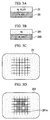
- FIGS. 3A to 3D are drawings explaining a peel test (seal test) for evaluating the adhesion of the ASA film constituting the second electrode 16 of the solar cell 10.
- FIG. 3A is a cross-sectional diagram of a sample A in which an ASA film 21 is formed on a glass substrate 20 by sputtering.
- FIG 3B is a cross-sectional diagram of a sample B in which an Ag film 201 having the same film thickness as that of the above-mentioned ASA film is formed on a glass substrate 200 (which is the same as the glass substrate 20) by sputtering.
- FIG 3C is a top view showing the result of the peel test of the above-mentioned sample A
- FIG 3D is a top view showing the result of the peel test of the above-mentioned sample B.
- the ASA film and the Ag film of the samples A and B were divided into 5 ⁇ 5 grids by a cutter to obtain 25 film pieces from each.
- an adhesive such as an adhesive tape was adhered and the adhesive was peeled off.
- adhesion of the respective films was evaluated.
- the same adhesives adheresives having the same adhesive power
- the adhesion with the glass substrate is evaluated.
- the second electrode 16 As described above, by forming the second electrode 16 with the alloy including Ag as a main component with Sn and Au added thereto, the adhesion between the second electrode 16 and the buffer layer 15 can be improved. As a result, since the contact resistance (interface resistance) of the interface between the second electrode and the buffer layer 15 can be decreased, the incident photon-to-current conversion efficiency of the solar cell can be improved.
- a plurality of the solar cells 10 were manufactured by changing the flow of argon gas in performing sputtering for forming the alloy electrode (second electrode 16) including Ag with Sn and Au added thereto.
- incident photon-to-current conversion efficiency was improved by about 7% as compared to the conventional solar cell having an Ag electrode as the second electrode 16.
- Table 1 it was confirmed that short-circuit current, open voltage, fill factor were also equal to or improved compared to the conventional case.
- values of the solar cell of this embodiment which has an ASA electrode as the second electrode 16 are shown when values in the conventional solar cell which has an Ag electrode as the second electrode 16 are set to 100 (%).
- the sample A in which the ASA film 21 was formed on the glass substrate 20 by sputtering
- the sample B in which an Ag film having the same film thickness as that of the ASA film of the sample A was formed on the same glass substrate as in the sample A
- These samples were dipped in saline water having a salt content of 5% for 96 hours and then the surfaces of both of the samples were visually observed.
- the corrosion resistance of the second electrode (alloy electrode) 16 can be improved. Accordingly, a decrease in reflectance due to the corrosion of the alloy electrode 16 can be prevented, and a decrease in contact resistance due to deterioration in adhesion at the interface between the second electrode and the buffer layer 15 can be prevented. As a result, it is possible to secure a stable high reflectance with little deterioration and it is possible to secure stabilized adhesion with no deterioration.
- the respective layers constituting the photoelectric conversion body 12, which are the first electrode (transparent electrode) 13, the n-i-p silicon film of the photoelectric conversion layer 14, the buffer layer 15 and the second electrode (alloy electrode) 16 composed of the ASA film 21, employ a texture structure in which irregularities are formed on the front and back surfaces.
- the incident photon-to-current conversion efficiency of the solar cell 10 can be further improved.
- the coverage of the ASA film which is formed on the buffer layer 15 having such a texture structure further deteriorates than in the conventional Ag film, it becomes a factor in a decrease in adhesion with the buffer layer 15.
- the ASA film 21 which is used as the second electrode 16 in this embodiment is formed on the buffer layer 15 having a texture structure, the same coverage as in the conventional Ag film is obtained. Accordingly, adhesion with the buffer layer 15 having a texture structure can be secured at the same or a higher level than in the conventional case.
- the solar cell 10 of FIG. 1 is a single solar cell in which the photoelectric conversion layer 14 employs a single structure.
- the present invention also can be applied to a tandem solar cell in which the photoelectric conversion layer employs a tandem structure.
- the above-mentioned solar cell 10 is exemplified by a so-called super-straight-type in which light is incident from the transparent substrate.
- the alloy electrode (second electrode) 16 can be applied even when a so-called substrate-type in which the alloy electrode (second electrode) 16, the buffer layer 15, the photoelectric conversion layer 14 and the first electrode (surface transparent electrode) 13 are formed on a substrate such as glass, an insulating material or a film is employed.
- the buffer layer 15 also can be formed of a conductive material having a low refractive index.
- the refractive index of the GZO film is 2.05.
- the buffer layer also can be formed of a material having a refractive index equal to or less than 2.0.
- the buffer layer 15 composed of a GZO film also functions as a reflection layer for reflecting some of the light beams entering and transmitted through the photoelectric conversion layer 14 toward the photoelectric conversion layer 14, but not directing the above light beams toward the alloy electrode 16.
- the refractive index of the silicon film constituting the photoelectric conversion layer 14 is in the range of 3.8 to 4.0, the light beams which can be reflected are limited to light beams of which the incident angle is small.
- the incident photon-to-current conversion efficiency can be further improved without the reflection of these light beams by the alloy electrode 16.
- the buffer layer 15 having such a low refractive index for example, there is a silicon oxide film doped with n-type impurities such as phosphorus (P), arsenic (As), antimony (Sb), bismuth (Bi), lithium (Li) and magnesium (Mg) for a case in which the buffer layer is formed on an n-type amorphous silicon film.
- n-type impurities such as phosphorus (P), arsenic (As), antimony (Sb), bismuth (Bi), lithium (Li) and magnesium (Mg)
- p-type impurities such as boron (B), gallium (Ga), aluminum (Al), indium (In), thallium (T1) and beryllium (Be) for a case in which the buffer layer is formed on a p-type amorphous silicon film.
- an ASA film including Ag as a main component with Sn and Au contained therein is used as the second electrode.
- an Ag alloy film including Ag as a main component with only one of Sn and Au contained therein also can be used as the second electrode.
- a solar cell of the present invention As the material for a second electrode, an alloy including Ag as a main component with Sn and Au added thereto is used. In this manner, reflectance of the metal electrode itself can be improved and adhesion with a buffer layer can be improved. Accordingly, since an increase in contact resistance at the interface is suppressed and incident photon-to-current conversion efficiency can thus be improved, the incident photon-to-current conversion efficiency and reliability of the solar cell can be improved (the adhesion is improved by adding Sn and the reflection characteristics and the corrosion resistance are improved by adding Au).
Landscapes
- Photovoltaic Devices (AREA)
Applications Claiming Priority (2)
| Application Number | Priority Date | Filing Date | Title |
|---|---|---|---|
| JP2008157713 | 2008-06-17 | ||
| PCT/JP2009/060700 WO2009154137A1 (ja) | 2008-06-17 | 2009-06-11 | 太陽電池およびその製造方法 |
Publications (2)
| Publication Number | Publication Date |
|---|---|
| EP2293344A1 true EP2293344A1 (de) | 2011-03-09 |
| EP2293344A4 EP2293344A4 (de) | 2013-03-06 |
Family
ID=41434052
Family Applications (1)
| Application Number | Title | Priority Date | Filing Date |
|---|---|---|---|
| EP09766585A Withdrawn EP2293344A4 (de) | 2008-06-17 | 2009-06-11 | Solarzelle und herstellungsverfahren dafür |
Country Status (7)
| Country | Link |
|---|---|
| US (1) | US20110108114A1 (de) |
| EP (1) | EP2293344A4 (de) |
| JP (1) | JPWO2009154137A1 (de) |
| KR (1) | KR101153435B1 (de) |
| CN (1) | CN101971357A (de) |
| TW (1) | TW201010100A (de) |
| WO (1) | WO2009154137A1 (de) |
Families Citing this family (5)
| Publication number | Priority date | Publication date | Assignee | Title |
|---|---|---|---|---|
| JP2011192896A (ja) * | 2010-03-16 | 2011-09-29 | Fuji Electric Co Ltd | 薄膜太陽電池およびその製造方法 |
| KR101273179B1 (ko) * | 2011-09-20 | 2013-06-17 | 엘지이노텍 주식회사 | 태양전지 및 이의 제조방법 |
| US20130081688A1 (en) * | 2011-10-03 | 2013-04-04 | Intermolecular, Inc. | Back contacts for thin film solar cells |
| EP2800146A1 (de) * | 2013-05-03 | 2014-11-05 | Saint-Gobain Glass France | Rückseitenkontaktiertes Substrat für eine Photovoltaikzelle oder ein Photovoltaikmodul |
| US11227961B2 (en) | 2013-10-25 | 2022-01-18 | Sharp Kabushiki Kaisha | Photoelectric conversion device |
Family Cites Families (13)
| Publication number | Priority date | Publication date | Assignee | Title |
|---|---|---|---|---|
| JPS59201471A (ja) * | 1983-04-29 | 1984-11-15 | Semiconductor Energy Lab Co Ltd | 光電変換半導体装置 |
| JP3078937B2 (ja) * | 1992-12-28 | 2000-08-21 | キヤノン株式会社 | 太陽電池とその製造方法 |
| JP2000286437A (ja) * | 1998-06-12 | 2000-10-13 | Canon Inc | 太陽電池モジュールおよび製造方法 |
| JP3365762B2 (ja) | 2000-04-28 | 2003-01-14 | 株式会社神戸製鋼所 | 光情報記録媒体用の反射層または半透明反射層、光情報記録媒体及び光情報記録媒体用スパッタリングターゲット |
| SG116432A1 (en) * | 2000-12-26 | 2005-11-28 | Kobe Steel Ltd | Reflective layer or semi-transparent reflective layer for use in optical information recording media, optical information recording media and sputtering target for use in the optical information recording media. |
| JP2003031824A (ja) * | 2001-07-13 | 2003-01-31 | Sharp Corp | 太陽電池モジュール |
| JP2003174177A (ja) * | 2001-12-05 | 2003-06-20 | Mitsubishi Heavy Ind Ltd | 太陽電池 |
| JP4671579B2 (ja) * | 2002-12-16 | 2011-04-20 | 株式会社アルバック | Ag合金反射膜およびその製造方法 |
| WO2004066354A2 (en) * | 2003-01-16 | 2004-08-05 | Target Technology Company, Llc | Photo-voltaic cells including solar cells incorporating silver-alloy reflective and/or transparent conductive surfaces |
| JP4714477B2 (ja) | 2004-02-19 | 2011-06-29 | アルバック成膜株式会社 | Ag合金膜及びその製造方法 |
| JPWO2005109524A1 (ja) * | 2004-05-07 | 2008-03-21 | 三菱電機株式会社 | 太陽電池及びその製造方法 |
| JP2006098856A (ja) * | 2004-09-30 | 2006-04-13 | Ulvac Japan Ltd | Ag系反射膜およびその作製方法 |
| JP2007266095A (ja) | 2006-03-27 | 2007-10-11 | Mitsubishi Heavy Ind Ltd | 光電変換セル、光電変換モジュール、光電変換パネルおよび光電変換システム |
-
2009
- 2009-06-11 EP EP09766585A patent/EP2293344A4/de not_active Withdrawn
- 2009-06-11 WO PCT/JP2009/060700 patent/WO2009154137A1/ja not_active Ceased
- 2009-06-11 CN CN2009801087368A patent/CN101971357A/zh active Pending
- 2009-06-11 JP JP2010517884A patent/JPWO2009154137A1/ja active Pending
- 2009-06-11 KR KR1020107020578A patent/KR101153435B1/ko not_active Expired - Fee Related
- 2009-06-11 US US12/933,332 patent/US20110108114A1/en not_active Abandoned
- 2009-06-15 TW TW098119972A patent/TW201010100A/zh unknown
Also Published As
| Publication number | Publication date |
|---|---|
| EP2293344A4 (de) | 2013-03-06 |
| JPWO2009154137A1 (ja) | 2011-12-01 |
| KR20100115369A (ko) | 2010-10-27 |
| KR101153435B1 (ko) | 2012-06-07 |
| WO2009154137A1 (ja) | 2009-12-23 |
| CN101971357A (zh) | 2011-02-09 |
| US20110108114A1 (en) | 2011-05-12 |
| TW201010100A (en) | 2010-03-01 |
Similar Documents
| Publication | Publication Date | Title |
|---|---|---|
| US6825409B2 (en) | Method for producing solar cells and thin-film solar cell | |
| KR101645045B1 (ko) | 태양광 모듈 | |
| US8779281B2 (en) | Solar cell | |
| US10014426B2 (en) | Solar cell and solar cell module | |
| US20130312829A1 (en) | Photoelectric conversion element | |
| Gouillart et al. | Reflective back contacts for ultrathin Cu (In, Ga) Se 2-based solar cells | |
| US20170162725A1 (en) | Solar cell | |
| US20110108114A1 (en) | Solar cell and method of manufacturing same | |
| JP7854985B2 (ja) | 透明導電層、および該透明導電層を備える光起電デバイス | |
| JP5362016B2 (ja) | 太陽電池およびその製造方法 | |
| JP2002118273A (ja) | 集積型ハイブリッド薄膜光電変換装置 | |
| CN103718307A (zh) | 具有减小的功率损耗的太阳能模块及其制造方法 | |
| RU2455730C2 (ru) | Солнечный элемент | |
| KR101305880B1 (ko) | 태양전지 및 이의 제조방법 | |
| JP4568531B2 (ja) | 集積型太陽電池及び集積型太陽電池の製造方法 | |
| KR101814821B1 (ko) | 태양전지 모듈 | |
| US20140130858A1 (en) | Solar cell | |
| US20120090664A1 (en) | Photovoltaic device | |
| JPH06338623A (ja) | 薄膜太陽電池 | |
| JP5468217B2 (ja) | 薄膜太陽電池 | |
| JP2010171127A (ja) | 薄膜太陽電池およびその製造方法 | |
| JP4988231B2 (ja) | 光電変換装置 | |
| US20120048330A1 (en) | Thin film solar cell module and fabricating method thereof | |
| CN121240610B (zh) | 光伏电池及其制备方法、光伏组件 | |
| JP2015141941A (ja) | 太陽電池および太陽電池モジュール |
Legal Events
| Date | Code | Title | Description |
|---|---|---|---|
| PUAI | Public reference made under article 153(3) epc to a published international application that has entered the european phase |
Free format text: ORIGINAL CODE: 0009012 |
|
| 17P | Request for examination filed |
Effective date: 20110117 |
|
| AK | Designated contracting states |
Kind code of ref document: A1 Designated state(s): AT BE BG CH CY CZ DE DK EE ES FI FR GB GR HR HU IE IS IT LI LT LU LV MC MK MT NL NO PL PT RO SE SI SK TR |
|
| AX | Request for extension of the european patent |
Extension state: AL BA RS |
|
| DAX | Request for extension of the european patent (deleted) | ||
| A4 | Supplementary search report drawn up and despatched |
Effective date: 20130201 |
|
| RIC1 | Information provided on ipc code assigned before grant |
Ipc: H01L 31/0224 20060101AFI20130128BHEP Ipc: H01L 31/052 20060101ALI20130128BHEP |
|
| STAA | Information on the status of an ep patent application or granted ep patent |
Free format text: STATUS: THE APPLICATION IS DEEMED TO BE WITHDRAWN |
|
| 18D | Application deemed to be withdrawn |
Effective date: 20130903 |