EP2290831A2 - Übertragungsvorrichtung und -verfahren - Google Patents
Übertragungsvorrichtung und -verfahren Download PDFInfo
- Publication number
- EP2290831A2 EP2290831A2 EP10172412A EP10172412A EP2290831A2 EP 2290831 A2 EP2290831 A2 EP 2290831A2 EP 10172412 A EP10172412 A EP 10172412A EP 10172412 A EP10172412 A EP 10172412A EP 2290831 A2 EP2290831 A2 EP 2290831A2
- Authority
- EP
- European Patent Office
- Prior art keywords
- voltage control
- timing
- control signal
- signal
- transmission
- Prior art date
- Legal status (The legal status is an assumption and is not a legal conclusion. Google has not performed a legal analysis and makes no representation as to the accuracy of the status listed.)
- Granted
Links
Images









Classifications
-
- H—ELECTRICITY
- H03—ELECTRONIC CIRCUITRY
- H03G—CONTROL OF AMPLIFICATION
- H03G3/00—Gain control in amplifiers or frequency changers
- H03G3/20—Automatic control
- H03G3/30—Automatic control in amplifiers having semiconductor devices
- H03G3/3036—Automatic control in amplifiers having semiconductor devices in high-frequency amplifiers or in frequency-changers
-
- H—ELECTRICITY
- H04—ELECTRIC COMMUNICATION TECHNIQUE
- H04B—TRANSMISSION
- H04B1/00—Details of transmission systems, not covered by a single one of groups H04B3/00 - H04B13/00; Details of transmission systems not characterised by the medium used for transmission
- H04B1/02—Transmitters
- H04B1/04—Circuits
- H04B2001/0408—Circuits with power amplifiers
- H04B2001/0416—Circuits with power amplifiers having gain or transmission power control
Definitions
- a certain aspect of the embodiments discussed herein is related to a mobile communication system, particularly to a delay adjusting method for voltage signals and transmission signals to be supplied to a voltage-controlled amplifier in a transmission device.
- An improvement in power efficiency is beneficial to transmission devices of wireless communication systems because miniaturization and energy conservation are advancing in the transmission devices.
- a drain or gate voltage control technique for realizing highly efficient amplification by controlling a voltage applied to a drain or gate electrode as described in Japanese Laid-open Patent Publication No. 2008-22513 .
- timings of a signal input to the power amplifier and a voltage control signal may be matched for obtaining a predetermined output in the drain or gate voltage control technique.
- Another example of adjusting delay of the voltage-controlled amplifier is as follows.
- a transmission signal or a voltage control signal is delayed by a delay circuit on a transmission side.
- Out-of-band emission power is measured using a feedback signal of a part of the output signal from the power amplifier when the transmission or voltage control signal is delayed.
- a delay amount is estimated using the magnitude of the out-of-band emission power.
- the delay amount is set in the delay circuit on the transmission side, and the feedback signal is analyzed to thereby estimate the delay amount. Since the delay amount is set in the delay circuit on the transmission side in order to estimate a delay amount, spurious signals may be output while the delay of the voltage-controlled amplifier is adjusted.
- the present invention is provided in order to solve one of the above-described problems.
- a transmission device including a voltage control signal generating unit configured to generate a first voltage control signal from a transmission signal, an amplifier configured to amplify the transmission signal in response to the first voltage control signal, a first timing adjusting unit configured to adjust a control timing for the first voltage control signal, and a control timing setting unit configured to set the control timing adjusted by the first timing adjusting unit based on the output signal from the amplifier and the transmission signal.
- FIG. 1 is an example block diagram illustrating a function of a wireless communication system of the Embodiment.
- the present system includes a base station (BS) 100 and a user equipment (UE) 200.
- BS base station
- UE user equipment
- the base station (BS) 100 includes a transmitting unit 102, a receiving unit 104, and a base band processing unit 106.
- the receiving unit 102 down-converts a radio signal received by an antenna into an intermediate frequency (IF), and outputs the down-converted radio signal to the base band processing unit 106.
- the base band processing unit 106 processes the signal input from the receiving unit 102 and sends the processed signal to a wired communication network.
- the signal sent from the wired communication network is processed by the base band processing unit 106 and input to the transmitting unit 102.
- the transmitting unit 102 up-converts the signal input to the base band processing unit 106 into a radio frequency (RF) band, amplifies the up-converted signal, and sends the amplified signal.
- RF radio frequency
- the user equipment (UE) 200 includes a transmitting unit 202, a receiving unit 204, and a base band processing unit 206.
- the receiving unit 202 transforms a high frequency signal received by the antenna and outputs the transformed signal to the base band unit 206.
- the base band processing unit 206 transforms the signal input by the receiving unit 202 to an analog signal.
- the analog signal transformed by the base band processing unit 206 is amplified and output from a speaker.
- an audio signal input by a microphone is input in the base band processing unit 206.
- the base band processing unit 206 transforms the input audio signal into a digital signal, and outputs the input audio signal to the transmitting unit 202.
- the transmitting unit 202 amplifies the digital signal input from the base band processing unit 206, and transmits the digital signal to the base station (BS) 100 with radio transmission.
- BS base station
- a transmission device 300 illustrated in FIG. 2 to be described later is applicable to at least one of the base station (BS) 100 and the user equipment (UE) 200.
- the transmission device 300 is applicable to at least one of a transmitting unit 102 of the base station 100 and a transmitting unit 202 of the user equipment (UE) 200.
- the transmission device 300 of the Embodiment is applicable to an apparatus including an amplifier which amplifies the input signal and outputs the amplified signal.
- the transmission device 300 is applicable to a personal digital assistance (PDA), a portable phone, or the like.
- PDA personal digital assistance
- portable phone or the like.
- the transmission device 300 is described in detail.
- FIG. 2 is an example block diagram illustrating a part of the transmission device 300 of the Embodiment.
- the transmission device 300 includes a voltage control signal transforming circuit 302, a timing adjusting circuit 304, a modulator 310, an oscillator 312, an amplifier 314, a memory 316, a timing error detecting unit 318, a memory 320, a mixer 324, and an oscillator 326.
- a transmission signal is transformed into a voltage control signal.
- the voltage control signal may be used to set a gain for amplifying the transmission signal by the amplifier 314.
- the gain may be set for a predetermined unit time based on the amplitude of the transmission signal in the predetermined unit time.
- the transmission device 300 controls the transmission signal and the voltage signal to match input timings of the transmission signal and the voltage control signal in the amplifier 314.
- the transmission device 300 acquires a delay amount of the voltage control signal relative to the transmission signal in order to minimize a timing shift between the transmission signal and the signal amplified by the amplifier 314.
- an appropriate amplification is obtainable in response to the level of the transmission signal. Since a desirable amplification is obtainable in response to the strength and type of the transmission signal, amplification efficiency can be improved. Further since the amplification efficiency is improved, power efficiency can also be improved.
- the process of acquiring the delay amount of the voltage control signal and the process of amplifying of the transmission signal are independently carried out. Accordingly, the delay amount is not changed while electric waves are transmitted. Therefore, the delay amount may be set without outputting spurious waves.
- the transmission device 300 includes a voltage control signal transforming circuit 302.
- the voltage control signal transforming circuit 302 is connected to a base band processing unit such as the band processing unit 106 or 206 illustrated in FIG. 1 .
- the voltage control signal transforming circuit 302 transforms a digital signal input from the base band processing unit as the transmission signal, and outputs the voltage control signal to the timing adjusting circuit 304.
- the transmission device 300 includes the timing adjusting circuit 304.
- the timing adjusting circuit 304 is connected to the voltage control signal transforming circuit 302.
- the timing adjusting circuit 304 adjusts a timing of the voltage control signal input from the voltage control signal transforming circuit 302 in conformity with a delay set amount set by the timing error detecting circuit 318 described later. For example, the timing of the voltage control signal supplied to the amplifier 314 is adjusted.
- the transmission device 300 includes a modulator 310.
- the modulator 310 is connected to the base band processing unit.
- the modulator 310 modulates the input transmission signal using a signal from the oscillator 312 included in the transmission device 300, and outputs the modulated signal to the amplifier 314.
- the transmission device 300 includes the modulator 312.
- the oscillator 312 is connected to the modulator 310, and outputs an oscillation signal to the modulator 310.
- the transmission device 300 includes the amplifier 314.
- the amplifier 314 is connected to the modulator 310.
- the amplifier 314 amplifies the input signal from the modulator 310 and outputs the amplified signal.
- the output signal is output to the mixer 324 described later.
- the output signal from the amplifier 314 is referred to as "feedback signal”.
- the transmission device 300 includes the mixer 324.
- the mixer 324 is connected to an output terminal of the amplifier 314.
- the mixer 324 down-converts the feedback signal into an IF frequency based on an oscillating frequency of the oscillator signal from the oscillator 326, and outputs the feedback signal to the memory 320.
- the transmission device 300 includes the oscillator 326.
- the oscillator 326 is connected to the mixer 324, and outputs an oscillation signal to the mixer 324.
- the transmission device 300 includes the memory 320.
- the memory 320 is connected to the mixer 324, and stores a digital signal output from the mixer 324.
- the transmission device 300 includes the memory 316.
- the memory 316 is connected to the base band processing unit, and stores the transmission signal.
- the transmission device 300 includes the timing adjusting circuit 318.
- the timing error detecting unit 318 is connected to the timing adjusting circuit 314, the memory 316, and the memory 320.
- the timing error detecting unit 318 acquires the delay set amount of the voltage control signal relative to the transmission signal to minimize a timing shift between the transmission signal and the voltage control signal in the amplifier 314 based on the transmission signal stored in the memory 316 and the digital signal stored in the memory 320.
- the digital signal is a feedback signal down-converted and transformed by the mixer 324.
- the timing error detecting unit 318 reads the transmission signal and the digital signal as time series data from the memory 316 and the memory 320, respectively.
- the timing error detecting unit 318 sets the acquired delay set amount in the timing adjusting circuit 304.
- the processes in the voltage control signal transforming circuit 302, the timing adjusting circuit 304, and the timing error detecting unit 318 may be carried out by transmitting and receiving digital signals.
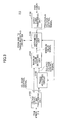
- FIG. 3 is an example block diagram illustrating a first mode of the timing error detecting unit 318 as a part of the transmission device 300 of the embodiment.
- the timing error detecting unit 318 includes a voltage control signal transforming unit 3182, a minimum value detecting unit 3184, an arithmetic processing unit 3186, an output signal transforming unit 3188, and a timing adjusting circuit 3190.
- the voltage control signal transforming unit 3182 is connected to the memory 316, the minimum value detecting unit 3184, and the timing adjusting circuit 3190.
- the voltage control signal transforming unit 3182 reads the transmission signal stored in the memory 316 as time series data, transforms the read time series data into the voltage control signal, and outputs the transformed voltage control signal to the minimum value detecting unit 3184 and the timing adjusting circuit 3190.
- the timing adjusting circuit 3190 is connected to the voltage control signal transforming unit 3182.
- the timing adjusting circuit 3190 adjusts the timing of the voltage control signal input from the voltage control signal transforming unit 3182, and outputs the adjusted voltage control signal to the minimum value detecting unit 3184.
- the voltage control signal is delayed by the timing adjusting circuit 3190 based on a delay set amount D2 which is set by an arithmetic processing unit 3186, and the timing adjusting circuit 3190 outputs the delayed voltage control signal to the minimum value detecting unit 3184.
- the voltage control signal delayed by the timing adjusting circuit 3190 is referred to as "delayed voltage control signal".
- the minimum value detecting unit 3184 is connected to the control signal transforming circuit 3182, the timing adjusting circuit 3190, and the arithmetic processing unit 3186.
- the minimum value detecting unit 3184 acquires the minimum value between the voltage control signal input from the voltage control signal transforming unit 3182 and the delayed voltage control signal input from the timing adjusting circuit 3190, and outputs the minimum value to the arithmetic processing unit 3186 as a signal equivalent to a signal output from the output signal transforming unit 3188 described later.
- the signal indicative of the minimum value is referred to as "minimum value signal”.
- FIG. 4 is a graph schematically illustrating an operation of the transmission device 300 in the minimum value detecting unit 3184 of the Embodiment.
- the abscissa represents time (t) and the ordinate represents envelope value.
- Solid lines designate the voltage control signal input from the voltage control signal transforming unit 3182.
- Broken lines designate the delayed voltage control signal which has been delayed based on the delay set amount D2 of the voltage control signal which is input by the timing adjusting circuit 3190.
- Heavy solid lines designate an output signal (minimum value signal) from the minimum value detecting unit 3184. The minimum value signal follows the smaller values between the values of the voltage control signal and the values of the delayed voltage control signal.
- the output signal transforming unit 3188 is connected to the memory 320.
- the output signal transforming unit 3188 reads the feedback signal processed as described above and stored in the memory 320 as time series data, provisionally transforms the time series data into a provisional voltage control signal (hereinafter, the voltage control signal provisionally transformed by the output signal transforming unit 3188 is referred to as "provisional voltage control signal"), and outputs the provisional voltage control signal to the arithmetic processing unit 3186.
- provisional voltage control signal is processed by the voltage control signal transforming circuit 302, the voltage control signal transforming unit 3182, and mixer 324 to be down-converted in a similar manner to the above, but is not actually used as the voltage control signal.
- FIG. 5 is a graph schematically illustrating an output signal from the amplifier 314 as the operation of the transmission device 300 of the Embodiment.
- the abscissa represents time (t) and the ordinate represents envelope value.
- Narrow solid lines designate the voltage control signal input from the timing adjusting circuit 304.
- Broken lines designate the transmission signal input from the modulator 310, i.e. the input signal to the amplifier 314.
- Heavy solid lines designate an output signal from the amplifier 314.
- the output signal has plural drop points. When the timings of the transmission signal and the voltage control signal match, an interval of the drops of the transmission signal and an interval of the drops of the output signals become equal. However, when the timings do not match, the interval of the drops of the transmission signal and the interval of the drops of the output signals become different. Therefore, the number of drops of the output signal increases.
- the arithmetic processing unit 3186 is connected to the timing adjusting circuit 304, the timing adjusting circuit 3190, the minimum value detecting unit 3184, and the output signal transforming unit 3188.
- the arithmetic processing unit 3186 compares the provisional voltage control signal input from the output signal transforming unit 3188 with the minimum value signal from the minimum value detecting unit 3184.
- the arithmetic processing unit 3186 acquires a timing error between the provisional voltage control signal and the minimum value signal.
- the arithmetic processing unit 3186 acquires a time error between the provisional voltage control signal and the minimum value signal.
- the time error may be a delay amount.
- the arithmetic processing unit 3186 may acquire a relationship between the provisional voltage control signal and the minimum value signal.
- the arithmetic processing unit 3186 temporarily stores the timing error, and changes the delay set amount D2 to be set in the timing adjusting circuit 3190.
- the arithmetic processing unit 3186 compares the provisional voltage control signal input from the output signal transforming unit 3188 with the minimum value signal from the minimum value detecting unit 3184 using the changed delay set amount D2.
- the arithmetic processing unit 3186 acquires a timing error between the provisional voltage control signal and the minimum value signal.
- the arithmetic processing unit 3186 acquires a time error between the provisional voltage control signal and the minimum value signal.
- the time error may be a delay amount.
- the arithmetic processing unit 3186 may acquire a relationship between the provisional voltage control signal and the minimum value signal.
- the arithmetic processing unit 3186 temporarily stores the timing error.
- the change of the delay set amount D2 may be carried out until the timing error is minimized, or the number of times changing the delay set amounts D2 may be preset.
- obtaining the correlation may be carried out until the correlation is maximized, or the number of times changing the delay set amount D2 may be preset.
- the timing error at a time of changing from decrementing to incrementing may be set as the minimum value up to which the delay set amount D2 is to be changed.
- the correlation at a time of changing from incrementing to decrementing may be set as the maximum value up to which the delay set amount D2 is to be changed.
- the arithmetic processing unit 3186 acquires a delay set amount D20 of a time when the timing error is minimized from the timing adjusting circuit 3190.
- the arithmetic processing unit 3186 may acquire the delay set amount D20 of a time when the correlation between the minimum value signal and the provisional voltage control signal is maximized from the timing adjusting circuit 3190.
- the arithmetic processing unit 3186 acquires the delay set amount D1 for the timing adjusting circuit 304 based on the acquired delay set amount D20.
- the arithmetic processing unit 3186 sets the delay set amount D1 in the timing adjusting circuit 304.
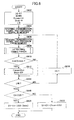
- FIG. 6 is an example flowchart of the operation in the transmission device 300 of the Embodiment.
- the reference symbol D1 designates the delay set amount for the timing adjusting circuit 304
- the reference symbol D2 designates a delay set amount for the timing adjusting circuit 3190.
- Reference symbol N designates the number of times repeating the process
- reference symbol Errmin designates a minimum (timing) error
- reference symbol Dmin designates a delay set amount causing the minimum error.
- the transmission device 300 sets parameters in step. For example, the transmission device 300 sets the same value to be the delay set amount D1 for the timing adjusting circuit 304 and the delay set amount D2 for the timing adjusting circuit 3190.
- the transmission device 300 may set N0 as the number N of times repeating the process.
- the transmission device 300 sets infinity (a very large number) ( ⁇ ) as the minimum error Errmin.
- the transmission device 300 sets zero (0) as the delay set amount Dmin causing the minimum error.
- the transmission device 300 sets zero (0) as the parameter i indicative of the number N of times repeating the process.
- the arithmetic processing unit 3186 sets up the delay set amounts D1 and D2, the number N of times repeating the process, the minimum error Errmin, the delay amount Dmin, and the parameter i indicative of the number N of times repeating the process.
- step S604 the transmission device 300 reads the transmission signal and the feedback signal into the memory.
- the memory 316 stores the transmission signal from the base band processing unit 106 or 206.
- the memory 320 stores the feedback signal processed as described above from the mixer 324.
- step S606 the transmission device 300 reads the transmission signal stored in the memory 316 and the feedback signal stored in the memory 320 as time-series data.
- the timing error detecting unit 318 reads the transmission signal stored in the memory 316 and the feedback signal processed as described above and stored in the memory 320 as time-series data.
- step S608 the transmission device 300 detects a timing error Erri.
- the timing error detecting unit 318 detects the timing error Erri between the minimum value signal and the provisional voltage control signal.
- the minimum value signal is obtained based on the transmission signal transformed into the voltage control signal and the delayed voltage control signal obtained by delaying the voltage control signal based on the delay amount D2.
- step S610 the transmission device 300 determines whether the timing detected in step S608 is less than the minimum error Errmin. For example, the timing error detecting unit 318 determines whether the timing error Erri is less than the minimum error Errmin.
- step S612 when the timing error Erri is less than the minimum error Errmin in YES of step S610, the transmission device 300 sets the minimum error Errmin to equal the timing error Erri, and sets the delay amount Dmin to equal the delay set amount D2. For example, when the timing error Erri is less than the minimum error Errmin, the timing error detecting unit 318 sets the minimum error Errmin to equal the timinig error Erri, and sets the delay amount Dmin to equal the delay set amount D2.
- step S614 when the timing error Erri is not less than the minimum error Errmin in No of step S610, i.e. the timing error Erri is greater than or equal to the minimum error Errmin, the transmission device 300 determines whether the parameter i is greater than the number N of times repeating the process. After the minimum error Errmin is set to equal the timing error Erri in step S612 and the delay amount Dmin is set to equal the delay set amount D2 in step S612, the transmission device 300 determines whether the parameter i is greater than the number N of times repeating the process also in step S614. The number N of times repeating the process may be preset. For example, the timing error detecting unit 318 determines whether the parameter i is greater than the number N of times repeating the process.
- step S618 when the parameter i is greater than the number N of repeating the process in YES of step S614, the transmission device 300 determines whether the delay set amount D1 for the timing adjusting circuit 304 is less than the delay set amount D20 causing the delay amount to be zero in the timing adjusting circuit 3190.
- the timing error detecting unit 318 determines whether the delay set amount D1 for the timing adjusting circuit 304 is less than the delay set amount D20 causing the delay amount to be zero in the timing adjusting circuit 3190.
- step S616 when the parameter i is less than or equal to the number N of times repeating the process in NO of step S614, the transmission device 300 increments the parameter i to i+1. Thereafter, the process goes back to step S606.
- the delay set amount D2 is set again, and the timing error is detected.
- step S620 when the delay set amount D1 for the timing adjusting circuit 304 is determined to be less than the delay set amount D20 in YES of step S618, the transmission device 300 acquires a value by subtracting the delay amount Dmin from the delay set amount D20 and then adding the delay set amount D1 to be the subtracted value, and sets the added value to the delay set amount D1.
- the delay set amount D1 to be set in the timing adjusting circuit 304 is acquired with the formula D1+(D20-Dmin).
- the timing error detecting unit 318 acquires a value by subtracting the delay amount Dmin as the minimum error from the delay set amount D20, and adds the delay set amount D1 to the subtracted value.
- the added value is set to be the delay set amount D1 to be set in the timing adjusting circuit 304.
- step S622 when the delay set amount D1 for the timing adjusting circuit 304 is determined not to be less than the delay set amount D20 causing the delay amount to be zero in the timing adjusting circuit 3190 in NO of step S618, i.e. the delay set amount D1 for the timing adjusting circuit 304 is greater than or equal to the delay circuit amount D20 causing the delay amount in the timing adjusting circuit 3190 to be zero, the transmission device 300 acquires a value by subtracting the delay set amount D20 from the delay amount Dmin and then subtracting the subtracted value from the delay set amount D1, and sets the subtracted value to be the delay set amount D1.
- the delay set amount D1 to be set in the timing adjusting circuit 304 is acquired with the formula D1-(Dmin-D20).
- the timing error detecting unit 318 acquires a value by subtracting the delay set amount D20 from the delay amount Dmin as the minimum error, and subtracts the subtracted value from the delay set amount D1.
- the subtracted value is set as the delay set amount D1 to be set in the timing adjusting circuit 304.
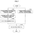
- FIG. 7 is an example flowchart of the operation of the timing error detecting unit 318 in the transmission device 300 of the Embodiment.
- step S702 the timing error detecting unit 318 transforms the transmission signal into the voltage control signal.
- the voltage control signal transforming unit 3182 reads the transmission signal stored in the memory 316, and transforms the read transmission signal into the voltage control signal.
- step S704 the timing error detecting unit 318 sets the output delay set amount D2 for the voltage control signal in the timing adjusting circuit 3190.
- the arithmetic processing unit 3186 sets the output delay set amount D2 in the timing adjusting circuit 3190.
- step S706 the timing error detecting unit 318 detects the minimum value based on the voltage control signal and the delayed voltage control signal obtained by delaying the voltage control signal using the delay set amount D2.
- the minimum value detecting unit 3184 detects the minimum value based on the voltage control signal and the delayed voltage control signal.
- the minimum value signal is output from the minimum value detecting unit 3184.
- step S708 the timing error detecting unit 318 transforms the feedback signal which is processed as described above into the provisional voltage control signal.
- the output signal transforming unit 3188 reads the feedback signal stored in the memory 320 as time series data, and transforms the time series data into the provisional voltage control signal.
- the timing error detecting unit 318 acquires the timing error Erri based on the minimum value signal and the provisional voltage control signal.
- the arithmetic processing unit 3186 compares the provisional voltage control signal input from the output signal transforming unit 3188 with the minimum value signal from the minimum value detecting unit 3184.
- the arithmetic processing unit 3186 acquires the timing error Erri between the provisional voltage control signal and the minimum value signal.
- the arithmetic processing unit 3186 obtains a time error between the provisional voltage control signal and the minimum value signal.
- the time error may be a delay amount.
- the delay set amount may be provided to the transmission signal.
- the timing adjusting circuit may be provided between the base band processing unit 206 and the amplifier 314.
- the transmission device of the Embodiment can adjust the delay without outputting spurious waves since the delay set amount is estimated using a portion which does not relate to transmission of the signals.
- the transmission data stored in the memory is read as the time series data, the voltage control signal is generated from the time series data, and the delayed voltage control signal is generated by the delay circuit. Further, by detecting the minimum value between the voltage control signal and the delayed voltage control signal, a signal corresponding to the output signal from the amplifier 314, i.e. a signal equivalent to the output signal from the amplifier 314, can be generated.
- the feedback signal from the amplifier 314 is read as the time series data, and the provisional voltage control signal is generated from the time series data.
- the delay amount causing the timing error between the minimum value signal equivalent to the output signal from the amplifier 314 and the provisional voltage control signal to be minimum is obtained, and a control timing of the voltage control signal or the transmission signal in the amplifier 314 is corrected by the delay amount.
- the timing error between the minimum value signal equivalent to the output signal from the amplifier 314 and the provisional voltage control signal may be determined in comparison with a reference value.
- FIG. 8 is an example block diagram illustrating a second mode of the timing error detecting unit 318 as a part of the transmission device 300 of the Embodiment.
- the timing error detecting unit 318 includes a voltage control signal transforming unit 3182, a timing adjusting circuit 3190, a gain adjusting unit 3192, a multiplier 3194, and an arithmetic processing unit 3196.
- the voltage control signal transforming unit 3182 is connected to the memory 316.
- the voltage control signal transforming unit 3182 reads the transmission signal stored in the memory 316 as time series data, transforms the time series data into a voltage control signal B, and outputs the voltage control signal B to the gain adjusting unit 3192 and the timing adjusting circuit 3190.
- the timing adjusting circuit 3190 is connected to the voltage control signal transforming unit 3182.
- the timing adjusting circuit 3190 adjusts the timing of the voltage control signal input from the voltage control signal transforming unit 3182, and outputs the adjusted voltage control signal (hereinafter referred to as timing-adjusted signal A) to the gain adjusting unit 3192.
- the timing adjusting circuit 3190 adjusts the voltage control signal based on a delay set amount D2 set by the arithmetic processing unit 3196, and outputs the adjusted voltage control signal to the gain adjusting unit 3192.
- the timing may be a timing of inputting to the gain adjusting unit 3192.
- the gain adjusting unit 3192 is connected to the voltage control signal transforming unit 3182, and the timing adjusting circuit 3190.
- the gain adjusting unit 3192 determines a gain adjusting value based on the voltage control signal B input from the voltage control signal transforming unit 3182 and the timing-adjusted signal A which is obtained by adjusting the timing of the voltage control signal with the timing adjusting circuit 3190.
- the amplitude of the timing-adjusted signal A is divided by the amplitude of the voltage control signal B in order to acquire the gain adjusting value.
- the gain adjusting unit 3192 sets the gain adjusting value as 1.
- the gain adjusting unit 3192 sets the gain adjusting value as 1.
- the amplitude of the voltage control signal B is divided by the amplitude of the timing-adjusted signal A in order to acquire the gain adjusting value.
- the gain adjusting unit 3192 outputs the gain adjusting value to the multiplier 3194.
- the multiplier 3194 is connected to the memory 316 and the gain adjusting unit 3192.
- the multiplier 3194 multiplies the transmission signal read as the time series data from the memory 316 by the gain adjusting value input from the gain adjusting unit 3192, and outputs the multiplied signal to the arithmetic processing unit 3196.
- the signal output from the multiplier 3194 is referred to as "gain-adjusted transmission signal”.
- FIG. 9 is a graph schematically illustrating the signal output from the multiplier 3194 in the transmission device 300 of the Embodiment.
- the abscissa represents time (t) and the ordinate represents envelope value.
- Narrow solid lines designate the voltage control signal B input from the voltage control signal transforming unit 3182.
- Broken lines designate the timing-adjusted signal A in which the timing of the voltage control signal is adjusted using the delay set amount D2 and which is input from the timing adjusting circuit 3190.
- Heavy solid lines designate an output signal (gain-adjusted transmission signal) from the multiplier 3194.
- the arithmetic processing unit 3196 is connected to the multiplier 3194, the timing adjusting circuit 304, and the timing adjusting circuit 3190.
- the arithmetic processing unit 3196 compares time series data of the feedback signal which have been processed as described above and stored in the memory 320 with the gain-adjusted transmission signal input from the multiplier 3194.
- the arithmetic processing unit 3196 obtains a timing error between the time series data of the feedback signal and the gain-adjusted transmission signal.
- the arithmetic processing unit 3196 acquires a time error between the gain-adjusted transmission signal and the time-series data which have been processed as described above.
- the time error may be a delay amount.
- the arithmetic processing unit 3196 temporarily stores the timing error, and changes the delay set amount D2 to be set to the timing adjusting circuit 3190.
- the arithmetic processing unit 3196 compares the time series data of the feedback signal processed as described above and stored in the memory 320 with the gain-adjusted transmission signal input from the multiplier 3194.
- the arithmetic processing unit 3196 acquires a timing error between the time series data and the gain-adjusted transmission signal.
- the arithmetic processing unit 3196 acquires a relationship between the gain-adjusted transmission signal and the time-series data processed as described above.
- the arithmetic processing unit 3196 temporarily stores the timing error.
- the change of the delay set amount D2 may be carried out until the timing error is minimized, or the number of times changing the delay set amounts D2 may be preset.
- a correlation is obtained, it may be carried out until the correlation is maximized, or the number of changing the delay set amount D2 may be preset.
- the timing error at a time of changing from decrementing to incrementing may be set as the minimum value up to which the delay set amount D2 is changed.
- the correlation of a time of changing from incrementing to decrementing may be set as the maximum value up to which the delay set amount D2 is changed.
- the arithmetic processing unit 3196 acquires the delay set amount Dmin of a time when the timing error is minimized from the timing adjusting circuit 3190.
- the arithmetic processing unit 3196 may acquire the delay set amount of a time when the correlation is maximized from the timing adjusting circuit 3190.
- the arithmetic processing unit 3196 acquires the delay set amount D1 for the timing adjusting circuit 304 based on the acquired delay set amount Dmin.
- the arithmetic processing unit 3186 sets the delay set amount D1 in the timing adjusting circuit 304.
- the operation of the transmission device 300 is similar to that illustrated in FIG. 6 .
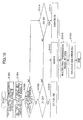
- FIG. 10 is an example flowchart of the operation of the timing error detecting unit 318 in the transmission device 300 of the Embodiment.
- step S1002 the timing error detecting unit 318 transforms the transmission signal into the voltage control signal B.
- the Voltage control signal transforming unit 3182 reads the transmission signal stored in the memory 316, and transforms the read transmission signal into the voltage control signal B.
- step S1004 the timing error detecting unit 318 sets an output delay set amount D2 for the voltage control signal to the timing adjusting circuit 3190.
- the arithmetic processing unit 3186 sets the output delay set amount D2 to the timing adjusting circuit 3190.
- step S1006 the timing error detecting unit 318 determines whether the voltage control signal B has an advanced phase in comparison with that of the timing-adjusted signal A in which the timing of the voltage control signal B is adjusted using the delay set amount D2 set to the timing adjusting circuit 3190.
- the gain adjusting unit 3192 determines whether the voltage control signal B has an advanced phase in comparison with that of the timing-adjusted signal A.
- step S1008 when it is determined that the voltage control signal B has an advanced phase in comparison with that of the timing-adjusted signal A in YES of step S1006, the timing error detecting unit 318 determines whether the amplitude
- step S1010 when the amplitude
- the gain adjusting unit 3192 acquires the gain adjusting value by dividing the amplitude
- step S1012 when the amplitude
- the gain adjusting unit 3192 sets the gain adjusting value as 1.
- step S1014 when it is determined that the voltage control signal B does not have an advanced phase in comparison with that of the timing-adjusted signal A in NO of step S1006, the timing error detecting unit 318 determines whether the amplitude
- step S1016 when the amplitude
- the gain adjusting unit 3192 acquires the gain adjusting value by dividing the amplitude
- step S1012 when the amplitude
- step S1018 the timing error detecting unit 318 multiplies the transmission signal by the gain adjusting value acquired in steps S1010, S1012 and S1016.
- the multiplier 3194 multiplies the transmission signal by the gain adjusting value input from the gain adjusting unit 3192.
- step S1020 the timing error detecting unit 318 acquires a timing error Erri based on the time series data processed as described above and the gain adjusted transmission signal.
- the arithmetic processing unit 3196 compares the gain-adjusted transmission signal input from the multiplier 3194 with the time series data obtained by reading the feedback signal which have been provided with predetermined process and stored in the memory 320.
- the arithmetic processing unit 3186 acquires the timing error Erri between the gain-adjusted transmission signal and the time-series data which have been processed as described above.
- the time error may be a delay amount.
- the transmission device 300 With the transmission device 300, it is possible to produce a signal corresponding to the feedback signal. Accordingly, without transforming the transmission signal to the voltage signal, the timing error is obtainable.
- FIG. 11 is an example block diagram illustrating a third mode of the timing error detecting unit 318 as a part of the transmission device 300 of the Embodiment.
- the timing error detecting unit 318 includes a voltage control signal transforming unit 3182, an arithmetic processing unit 3200, an output signal transforming unit 3188, a timing adjusting circuit 3190 and a maximum value detecting unit 3198.
- the voltage control signal transforming unit 3182 is connected to the memory 316.
- the voltage control signal transforming unit 3182 reads the transmission signal stored in the memory 316 as time series data, transforms the time series data into the voltage control signal, and outputs the transformed voltage control signal to the arithmetic processing unit 3200 and the timing adjusting circuit 3190.
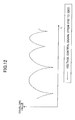
- FIG. 12 is a graph schematically illustrating an example of the voltage control signal in the transmission device 300 of the Embodiment.
- the abscissa represents time (t) and the ordinate represents envelope value.
- the timing adjusting circuit 3190 is connected to the voltage control signal transforming unit 3182.
- the timing adjusting circuit 3190 adjusts the timing of the voltage control signal input from the voltage control signal transforming unit 3182, and outputs the adjusted voltage control signal to the maximum value detecting unit 3198.
- the voltage control signal is delayed by the timing adjusting circuit 3190 based on a delay set amount D2 which is set by the arithmetic processing unit 3200, and the timing adjusting circuit 3190 outputs the delayed voltage control signal to the maximum value detecting unit 3198.
- the signal to be input to the maximum value detecting unit 3198 is referred to as "delayed voltage control signal".
- the output signal transforming unit 3188 is connected to the memory 320.
- the output signal transforming unit 3188 reads the feedback signal processed as described above and stored in the memory 320 as time series data, transforms the time series data into a provisional voltage control signal, and outputs the provisional voltage control signal to the maximum value detecting unit 3198.
- the voltage control signal provisionally transformed by the output signal transforming unit 3188 is referred to as "provisional voltage control signal”.
- provisional voltage control signal is processed by the voltage control signal transforming circuit 302 and the voltage control signal transforming unit 3182 using the feedback signal, and the mixer 324 to be down-converted in a similar manner to the above, but is not actually used as the voltage control signal.
- the minimum value detecting unit 3198 is connected to the output signal transforming unit 3188 and the timing adjusting circuit 3190.
- the maximum value detecting unit 3198 acquires the maximum value between the provisional voltage control signal input from the output signal transforming unit 3188 and the delayed voltage control signal input from the timing adjusting circuit 3190, and outputs the maximum value to the arithmetic processing unit 3200 as a signal equivalent to the voltage control signal output by the output signal transforming unit 3200.
- the signal indicative of the maximum value is referred to as "maximum value signal”.
- FIG. 13 is a graph schematically illustrating the output maximum value detecting unit 3198 as an operation of the transmission device 300 of the Embodiment.
- the abscissa represents time (t) and the ordinate represents envelope value.
- Narrow solid lines designate the provisional voltage control signal input from the output signal transforming unit 3188.
- Broken lines designate the delayed voltage control signal which has been delayed based on the delay set amount D2 of the voltage control signal which is input by the timing adjusting circuit 3190.
- Heavy solid lines designate an output signal (maximum value signal) from the maximum value detecting unit 3198. The maximum value signal follows the greater values between the values of the provisional voltage control signal and the values of the delayed voltage control signal.
- the arithmetic processing unit 3200 is connected to the timing adjusting circuit 304, the voltage control signal transforming unit 3182, the timing adjusting circuit 3190, and the maximum value detecting unit 3198.
- the arithmetic processing unit 3200 compares the voltage control signal input from the voltage control signal transforming unit 3182 with the maximum value signal from the maximum value detecting unit 3198.
- the arithmetic processing unit 3200 acquires a timing error between the voltage control signal and the maximum value signal.
- the time error may be a delay amount.
- the arithmetic processing unit 3200 acquires a time error between the provisional voltage control signal and the maximum value signal.
- the arithmetic processing unit 3200 may acquire a relationship between the voltage control signal and the maximum value signal.
- the arithmetic processing unit 3200 temporarily stores the timing error, and changes the delay set amount D2 to be set in the timing adjusting circuit 3190.
- the arithmetic processing unit 3200 compares the voltage control signal input from the voltage control signal transforming unit 3182 with the maximum value signal from the maximum value detecting unit 3198.
- the arithmetic processing unit 3200 acquires the timing error between the voltage control signal and the maximum value signal.
- the arithmetic processing unit 3200 acquires a time error between the voltage control signal and the maximum value signal.
- the time error may be a delay amount.
- the arithmetic processing unit 3200 may acquire a relationship between the voltage control signal and the maximum value signal.
- the arithmetic processing unit 3200 temporarily stores the timing error.
- the change of the delay set amount D2 may be carried out until the timing error is minimized, or the number of times changing the delay set amounts D2 may be preset.
- obtaining the correlation may be carried out until the correlation is maximized, or the number of times changing the delay set amount D2 may be preset.
- the timing error at a time of changing from decrementing to incrementing may be set as the minimum value.
- the correlation of a time of changing from incrementing to decrementing may be set as the maximum value up to which the delay set amount D2 is changed.
- the arithmetic processing unit 3200 acquires the delay set amount Dmin of a time when the timing error is minimized from the timing adjusting circuit 3190.
- the arithmetic processing unit 3200 acquires the delay set amount D1 for the timing adjusting circuit 304 based on the acquired delay set amount Dmin.
- the arithmetic processing unit 3200 sets the delay set amount D1 to the timing adjusting circuit 304.
- the operation of the transmission device 300 is similar to that illustrated in FIG. 6 .
- FIG. 14 is an example flowchart of the operation of the timing error detecting unit 318 in the transmission device 300 of the Embodiment.
- step S1402 the timing error detecting unit 318 transforms the transmission signal into the voltage control signal.
- the voltage control signal transforming unit 3182 reads the transmission signal stored in the memory 316, and transforms the read transmission signal into the voltage control signal.
- step S1404 the timing error detecting unit 318 sets the output delay set amount D2 for the voltage control signal in the timing adjusting circuit 3190.
- the arithmetic processing unit 3200 sets the output delay set amount D2 in the timing adjusting circuit 3190.
- step S1406 the timing error detecting unit 318 transforms the feedback signal processed as described above into the provisional voltage control signal.
- the output signal transforming unit 3188 reads the feedback signal processed as described above and stored in the memory 320 as time series data, and transforms the time series data into the provisional voltage control signal.
- step S1408 the timing error detecting unit 318 detects the maximum value based on the provisional voltage control signal and the delayed voltage control signal acquired by delaying the voltage control signal for the delay set amount D2 which is set by the timing adjusting circuit 3190.
- the maximum value detecting unit 3198 detects the maximum value based on the provisional voltage control signal and the delayed voltage control signal.
- the maximum value signal is output from the maximum value detecting unit 3198.
- the timing error detecting unit 318 acquires a timing error Err based on the maximum value signal and the voltage control signal produced by transforming the transmission signal.
- the arithmetic processing unit 3200 compares the voltage control signal input from the voltage control signal transforming unit 3182 with the maximum value signal from the maximum value detecting unit 3198.
- the arithmetic processing unit 3200 acquires the timing error Erri between the voltage control signal and the maximum value signal.
- the arithmetic processing unit 3200 acquires a time error between the voltage control signal and the maximum value signal.
- the time error may be a delay amount.
- a signal corresponding to the voltage control signal which is obtained by transforming the transmission signal may be produced from the output signal from the amplifier.
Landscapes
- Transmitters (AREA)
- Amplifiers (AREA)
Applications Claiming Priority (1)
| Application Number | Priority Date | Filing Date | Title |
|---|---|---|---|
| JP2009201247A JP5267389B2 (ja) | 2009-09-01 | 2009-09-01 | 送信装置及び送信方法 |
Publications (3)
| Publication Number | Publication Date |
|---|---|
| EP2290831A2 true EP2290831A2 (de) | 2011-03-02 |
| EP2290831A3 EP2290831A3 (de) | 2014-01-22 |
| EP2290831B1 EP2290831B1 (de) | 2017-06-28 |
Family
ID=43306216
Family Applications (1)
| Application Number | Title | Priority Date | Filing Date |
|---|---|---|---|
| EP10172412.8A Not-in-force EP2290831B1 (de) | 2009-09-01 | 2010-08-10 | Übertragungsvorrichtung und -verfahren |
Country Status (5)
| Country | Link |
|---|---|
| US (1) | US8433262B2 (de) |
| EP (1) | EP2290831B1 (de) |
| JP (1) | JP5267389B2 (de) |
| KR (1) | KR101201560B1 (de) |
| CN (1) | CN102006090B (de) |
Families Citing this family (1)
| Publication number | Priority date | Publication date | Assignee | Title |
|---|---|---|---|---|
| WO2015186577A1 (ja) * | 2014-06-02 | 2015-12-10 | 株式会社村田製作所 | 送信回路、高周波フロントエンド回路、送信信号の制御方法、および、高周波フロントエンドの送受信制御方法 |
Citations (1)
| Publication number | Priority date | Publication date | Assignee | Title |
|---|---|---|---|---|
| JP2008022513A (ja) | 2006-06-15 | 2008-01-31 | Hitachi Kokusai Electric Inc | 歪制御機能付き増幅装置 |
Family Cites Families (12)
| Publication number | Priority date | Publication date | Assignee | Title |
|---|---|---|---|---|
| JP3709316B2 (ja) * | 1999-05-28 | 2005-10-26 | 松下電器産業株式会社 | 通信装置及び通信方法 |
| US6366177B1 (en) * | 2000-02-02 | 2002-04-02 | Tropian Inc. | High-efficiency power modulators |
| US6882831B2 (en) * | 2001-12-07 | 2005-04-19 | Broadcom Corporation | Translational loop transmitter architecture employing channel power ratio measurements for modulation accuracy calibration |
| JP3985649B2 (ja) * | 2002-10-03 | 2007-10-03 | 松下電器産業株式会社 | 送信方法及び送信装置 |
| GB2404506B (en) * | 2003-07-31 | 2006-02-22 | Renesas Tech Corp | Method of ramping up output level of power amplifier of radio communication system,communication semiconductor integrated circuit,& radio communication system |
| JP3844352B2 (ja) * | 2003-08-07 | 2006-11-08 | 松下電器産業株式会社 | 送信装置 |
| US7480344B2 (en) * | 2004-09-30 | 2009-01-20 | Broadcom Corporation | Architectural techniques for envelope and phase signal alignment in RF polar transmitters using power amplifier feedback |
| US7333780B2 (en) * | 2004-03-03 | 2008-02-19 | Matsushita Electric Industrial Co., Ltd. | Polar modulation transmission apparatus and radio communication apparatus |
| WO2006054464A1 (ja) * | 2004-11-17 | 2006-05-26 | Matsushita Electric Industrial Co., Ltd. | 送信回路、送信方法、及びそれを用いた通信機器 |
| JP4652974B2 (ja) * | 2005-12-27 | 2011-03-16 | 富士通株式会社 | タイミング調整装置及びタイミング調整方法 |
| JP2007189438A (ja) * | 2006-01-12 | 2007-07-26 | Fujitsu Ltd | タイミング調整装置及びタイミング調整方法 |
| JP2009194575A (ja) * | 2008-02-13 | 2009-08-27 | Panasonic Corp | 送信装置 |
-
2009
- 2009-09-01 JP JP2009201247A patent/JP5267389B2/ja not_active Expired - Fee Related
-
2010
- 2010-08-05 US US12/850,998 patent/US8433262B2/en not_active Expired - Fee Related
- 2010-08-10 EP EP10172412.8A patent/EP2290831B1/de not_active Not-in-force
- 2010-08-30 KR KR1020100084028A patent/KR101201560B1/ko not_active Expired - Fee Related
- 2010-08-31 CN CN201010269304XA patent/CN102006090B/zh not_active Expired - Fee Related
Patent Citations (1)
| Publication number | Priority date | Publication date | Assignee | Title |
|---|---|---|---|---|
| JP2008022513A (ja) | 2006-06-15 | 2008-01-31 | Hitachi Kokusai Electric Inc | 歪制御機能付き増幅装置 |
Also Published As
| Publication number | Publication date |
|---|---|
| KR101201560B1 (ko) | 2012-11-14 |
| EP2290831A3 (de) | 2014-01-22 |
| KR20110025103A (ko) | 2011-03-09 |
| JP5267389B2 (ja) | 2013-08-21 |
| CN102006090A (zh) | 2011-04-06 |
| EP2290831B1 (de) | 2017-06-28 |
| US20110053531A1 (en) | 2011-03-03 |
| US8433262B2 (en) | 2013-04-30 |
| JP2011055178A (ja) | 2011-03-17 |
| CN102006090B (zh) | 2013-11-06 |
Similar Documents
| Publication | Publication Date | Title |
|---|---|---|
| US7519336B2 (en) | Method and arrangement for optimizing efficiency of a power amplifier | |
| US6388518B1 (en) | Distortion compensation apparatus | |
| KR101061329B1 (ko) | 왜곡 보상 장치, 무선 통신 장치 및 왜곡 보상 방법 | |
| US8837635B2 (en) | Controlling a transmit path based on monitored error vector magnitude (EVM) performance | |
| US9144042B2 (en) | Method for fast automatic power control of wireless transmitters | |
| US8792546B2 (en) | Transmission circuit | |
| US7170952B2 (en) | System and method for post filtering peak power reduction in communications systems | |
| US7792214B2 (en) | Polar modulation transmitter circuit and communications device | |
| JP2007300400A (ja) | 送信回路、送信方法、及びそれを用いた通信機器 | |
| WO2006054464A1 (ja) | 送信回路、送信方法、及びそれを用いた通信機器 | |
| EP2136524A2 (de) | Amplitudenunterdrückungsvorrichtung und Signalübertragungsvorrichtung | |
| JP4518968B2 (ja) | 送信回路 | |
| JP2006333450A (ja) | 極座標変調回路、極座標変調方法、集積回路および無線送信装置 | |
| US20060264190A1 (en) | System and method for linearizing nonlinear power amplifiers | |
| EP2290831A2 (de) | Übertragungsvorrichtung und -verfahren | |
| US8031803B2 (en) | Transmitter capable of suppressing peak of transmission signal | |
| JP2000183847A (ja) | 無線周波数信号受信装置、周波数調整方法、電力制御方法及びシンボルタイミング制御方法 | |
| US7532905B2 (en) | Filter device and transmission power control apparatus | |
| JP2000236286A (ja) | 通信装置 | |
| US20220191866A1 (en) | Radio frequency signal generation method and related apparatus | |
| EP1120907A1 (de) | Vorrichtung zum Verstärken von Signalen | |
| EP1405427B1 (de) | System und verfahren zur nachfilterung bei der spitzenleistungsreduktion in kommunikationssystemen | |
| CN102035487A (zh) | 一种用于分集接收的自动增益控制方法及装置 | |
| JP5925729B2 (ja) | 無線通信装置および干渉軽減制御方法 | |
| KR20250066403A (ko) | 크기 및 위상 조절가능한 평형 증폭기 |
Legal Events
| Date | Code | Title | Description |
|---|---|---|---|
| PUAI | Public reference made under article 153(3) epc to a published international application that has entered the european phase |
Free format text: ORIGINAL CODE: 0009012 |
|
| AK | Designated contracting states |
Kind code of ref document: A2 Designated state(s): AL AT BE BG CH CY CZ DE DK EE ES FI FR GB GR HR HU IE IS IT LI LT LU LV MC MK MT NL NO PL PT RO SE SI SK SM TR |
|
| AX | Request for extension of the european patent |
Extension state: BA ME RS |
|
| PUAL | Search report despatched |
Free format text: ORIGINAL CODE: 0009013 |
|
| AK | Designated contracting states |
Kind code of ref document: A3 Designated state(s): AL AT BE BG CH CY CZ DE DK EE ES FI FR GB GR HR HU IE IS IT LI LT LU LV MC MK MT NL NO PL PT RO SE SI SK SM TR |
|
| AX | Request for extension of the european patent |
Extension state: BA ME RS |
|
| RIC1 | Information provided on ipc code assigned before grant |
Ipc: H03G 3/00 20060101ALI20131216BHEP Ipc: H04B 1/38 20060101AFI20131216BHEP |
|
| 17P | Request for examination filed |
Effective date: 20140325 |
|
| RBV | Designated contracting states (corrected) |
Designated state(s): AL AT BE BG CH CY CZ DE DK EE ES FI FR GB GR HR HU IE IS IT LI LT LU LV MC MK MT NL NO PL PT RO SE SI SK SM TR |
|
| 17Q | First examination report despatched |
Effective date: 20161024 |
|
| REG | Reference to a national code |
Ref country code: DE Ref legal event code: R079 Ref document number: 602010043235 Country of ref document: DE Free format text: PREVIOUS MAIN CLASS: H04B0001380000 Ipc: H03G0003300000 |
|
| GRAP | Despatch of communication of intention to grant a patent |
Free format text: ORIGINAL CODE: EPIDOSNIGR1 |
|
| RIC1 | Information provided on ipc code assigned before grant |
Ipc: H04B 1/04 20060101ALI20170110BHEP Ipc: H03G 3/30 20060101AFI20170110BHEP |
|
| INTG | Intention to grant announced |
Effective date: 20170202 |
|
| GRAC | Information related to communication of intention to grant a patent modified |
Free format text: ORIGINAL CODE: EPIDOSCIGR1 |
|
| INTG | Intention to grant announced |
Effective date: 20170215 |
|
| GRAS | Grant fee paid |
Free format text: ORIGINAL CODE: EPIDOSNIGR3 |
|
| GRAA | (expected) grant |
Free format text: ORIGINAL CODE: 0009210 |
|
| AK | Designated contracting states |
Kind code of ref document: B1 Designated state(s): AL AT BE BG CH CY CZ DE DK EE ES FI FR GB GR HR HU IE IS IT LI LT LU LV MC MK MT NL NO PL PT RO SE SI SK SM TR |
|
| REG | Reference to a national code |
Ref country code: GB Ref legal event code: FG4D |
|
| RIN1 | Information on inventor provided before grant (corrected) |
Inventor name: HAMADA, HAJIME Inventor name: FUDABA, NOBUKAZU Inventor name: ISHIKAWA, HIROYOSHI Inventor name: UTSUNOMIYA, YUICHI Inventor name: NAGATANI, KAZUO |
|
| REG | Reference to a national code |
Ref country code: CH Ref legal event code: EP |
|
| REG | Reference to a national code |
Ref country code: AT Ref legal event code: REF Ref document number: 905658 Country of ref document: AT Kind code of ref document: T Effective date: 20170715 |
|
| REG | Reference to a national code |
Ref country code: FR Ref legal event code: PLFP Year of fee payment: 8 |
|
| REG | Reference to a national code |
Ref country code: IE Ref legal event code: FG4D |
|
| REG | Reference to a national code |
Ref country code: DE Ref legal event code: R096 Ref document number: 602010043235 Country of ref document: DE |
|
| PG25 | Lapsed in a contracting state [announced via postgrant information from national office to epo] |
Ref country code: HR Free format text: LAPSE BECAUSE OF FAILURE TO SUBMIT A TRANSLATION OF THE DESCRIPTION OR TO PAY THE FEE WITHIN THE PRESCRIBED TIME-LIMIT Effective date: 20170628 Ref country code: LT Free format text: LAPSE BECAUSE OF FAILURE TO SUBMIT A TRANSLATION OF THE DESCRIPTION OR TO PAY THE FEE WITHIN THE PRESCRIBED TIME-LIMIT Effective date: 20170628 Ref country code: FI Free format text: LAPSE BECAUSE OF FAILURE TO SUBMIT A TRANSLATION OF THE DESCRIPTION OR TO PAY THE FEE WITHIN THE PRESCRIBED TIME-LIMIT Effective date: 20170628 Ref country code: NO Free format text: LAPSE BECAUSE OF FAILURE TO SUBMIT A TRANSLATION OF THE DESCRIPTION OR TO PAY THE FEE WITHIN THE PRESCRIBED TIME-LIMIT Effective date: 20170928 Ref country code: GR Free format text: LAPSE BECAUSE OF FAILURE TO SUBMIT A TRANSLATION OF THE DESCRIPTION OR TO PAY THE FEE WITHIN THE PRESCRIBED TIME-LIMIT Effective date: 20170929 |
|
| PGFP | Annual fee paid to national office [announced via postgrant information from national office to epo] |
Ref country code: GB Payment date: 20170704 Year of fee payment: 8 Ref country code: DE Payment date: 20170802 Year of fee payment: 8 Ref country code: FR Payment date: 20170725 Year of fee payment: 8 |
|
| REG | Reference to a national code |
Ref country code: NL Ref legal event code: MP Effective date: 20170628 |
|
| REG | Reference to a national code |
Ref country code: LT Ref legal event code: MG4D |
|
| REG | Reference to a national code |
Ref country code: AT Ref legal event code: MK05 Ref document number: 905658 Country of ref document: AT Kind code of ref document: T Effective date: 20170628 |
|
| PG25 | Lapsed in a contracting state [announced via postgrant information from national office to epo] |
Ref country code: NL Free format text: LAPSE BECAUSE OF FAILURE TO SUBMIT A TRANSLATION OF THE DESCRIPTION OR TO PAY THE FEE WITHIN THE PRESCRIBED TIME-LIMIT Effective date: 20170628 Ref country code: LV Free format text: LAPSE BECAUSE OF FAILURE TO SUBMIT A TRANSLATION OF THE DESCRIPTION OR TO PAY THE FEE WITHIN THE PRESCRIBED TIME-LIMIT Effective date: 20170628 Ref country code: SE Free format text: LAPSE BECAUSE OF FAILURE TO SUBMIT A TRANSLATION OF THE DESCRIPTION OR TO PAY THE FEE WITHIN THE PRESCRIBED TIME-LIMIT Effective date: 20170628 Ref country code: BG Free format text: LAPSE BECAUSE OF FAILURE TO SUBMIT A TRANSLATION OF THE DESCRIPTION OR TO PAY THE FEE WITHIN THE PRESCRIBED TIME-LIMIT Effective date: 20170928 |
|
| PG25 | Lapsed in a contracting state [announced via postgrant information from national office to epo] |
Ref country code: CZ Free format text: LAPSE BECAUSE OF FAILURE TO SUBMIT A TRANSLATION OF THE DESCRIPTION OR TO PAY THE FEE WITHIN THE PRESCRIBED TIME-LIMIT Effective date: 20170628 Ref country code: AT Free format text: LAPSE BECAUSE OF FAILURE TO SUBMIT A TRANSLATION OF THE DESCRIPTION OR TO PAY THE FEE WITHIN THE PRESCRIBED TIME-LIMIT Effective date: 20170628 Ref country code: SK Free format text: LAPSE BECAUSE OF FAILURE TO SUBMIT A TRANSLATION OF THE DESCRIPTION OR TO PAY THE FEE WITHIN THE PRESCRIBED TIME-LIMIT Effective date: 20170628 Ref country code: RO Free format text: LAPSE BECAUSE OF FAILURE TO SUBMIT A TRANSLATION OF THE DESCRIPTION OR TO PAY THE FEE WITHIN THE PRESCRIBED TIME-LIMIT Effective date: 20170628 Ref country code: EE Free format text: LAPSE BECAUSE OF FAILURE TO SUBMIT A TRANSLATION OF THE DESCRIPTION OR TO PAY THE FEE WITHIN THE PRESCRIBED TIME-LIMIT Effective date: 20170628 |
|
| PG25 | Lapsed in a contracting state [announced via postgrant information from national office to epo] |
Ref country code: IT Free format text: LAPSE BECAUSE OF FAILURE TO SUBMIT A TRANSLATION OF THE DESCRIPTION OR TO PAY THE FEE WITHIN THE PRESCRIBED TIME-LIMIT Effective date: 20170628 Ref country code: IS Free format text: LAPSE BECAUSE OF FAILURE TO SUBMIT A TRANSLATION OF THE DESCRIPTION OR TO PAY THE FEE WITHIN THE PRESCRIBED TIME-LIMIT Effective date: 20171028 Ref country code: SM Free format text: LAPSE BECAUSE OF FAILURE TO SUBMIT A TRANSLATION OF THE DESCRIPTION OR TO PAY THE FEE WITHIN THE PRESCRIBED TIME-LIMIT Effective date: 20170628 Ref country code: PL Free format text: LAPSE BECAUSE OF FAILURE TO SUBMIT A TRANSLATION OF THE DESCRIPTION OR TO PAY THE FEE WITHIN THE PRESCRIBED TIME-LIMIT Effective date: 20170628 Ref country code: ES Free format text: LAPSE BECAUSE OF FAILURE TO SUBMIT A TRANSLATION OF THE DESCRIPTION OR TO PAY THE FEE WITHIN THE PRESCRIBED TIME-LIMIT Effective date: 20170628 |
|
| REG | Reference to a national code |
Ref country code: CH Ref legal event code: PL Ref country code: DE Ref legal event code: R097 Ref document number: 602010043235 Country of ref document: DE |
|
| PG25 | Lapsed in a contracting state [announced via postgrant information from national office to epo] |
Ref country code: MC Free format text: LAPSE BECAUSE OF FAILURE TO SUBMIT A TRANSLATION OF THE DESCRIPTION OR TO PAY THE FEE WITHIN THE PRESCRIBED TIME-LIMIT Effective date: 20170628 |
|
| PG25 | Lapsed in a contracting state [announced via postgrant information from national office to epo] |
Ref country code: LI Free format text: LAPSE BECAUSE OF NON-PAYMENT OF DUE FEES Effective date: 20170831 Ref country code: CH Free format text: LAPSE BECAUSE OF NON-PAYMENT OF DUE FEES Effective date: 20170831 Ref country code: DK Free format text: LAPSE BECAUSE OF FAILURE TO SUBMIT A TRANSLATION OF THE DESCRIPTION OR TO PAY THE FEE WITHIN THE PRESCRIBED TIME-LIMIT Effective date: 20170628 |
|
| PLBE | No opposition filed within time limit |
Free format text: ORIGINAL CODE: 0009261 |
|
| STAA | Information on the status of an ep patent application or granted ep patent |
Free format text: STATUS: NO OPPOSITION FILED WITHIN TIME LIMIT |
|
| REG | Reference to a national code |
Ref country code: IE Ref legal event code: MM4A |
|
| REG | Reference to a national code |
Ref country code: BE Ref legal event code: MM Effective date: 20170831 |
|
| 26N | No opposition filed |
Effective date: 20180329 |
|
| PG25 | Lapsed in a contracting state [announced via postgrant information from national office to epo] |
Ref country code: LU Free format text: LAPSE BECAUSE OF NON-PAYMENT OF DUE FEES Effective date: 20170810 |
|
| PG25 | Lapsed in a contracting state [announced via postgrant information from national office to epo] |
Ref country code: IE Free format text: LAPSE BECAUSE OF NON-PAYMENT OF DUE FEES Effective date: 20170810 |
|
| PG25 | Lapsed in a contracting state [announced via postgrant information from national office to epo] |
Ref country code: BE Free format text: LAPSE BECAUSE OF NON-PAYMENT OF DUE FEES Effective date: 20170831 Ref country code: SI Free format text: LAPSE BECAUSE OF FAILURE TO SUBMIT A TRANSLATION OF THE DESCRIPTION OR TO PAY THE FEE WITHIN THE PRESCRIBED TIME-LIMIT Effective date: 20170628 |
|
| PG25 | Lapsed in a contracting state [announced via postgrant information from national office to epo] |
Ref country code: MT Free format text: LAPSE BECAUSE OF NON-PAYMENT OF DUE FEES Effective date: 20170810 |
|
| REG | Reference to a national code |
Ref country code: DE Ref legal event code: R119 Ref document number: 602010043235 Country of ref document: DE |
|
| GBPC | Gb: european patent ceased through non-payment of renewal fee |
Effective date: 20180810 |
|
| PG25 | Lapsed in a contracting state [announced via postgrant information from national office to epo] |
Ref country code: HU Free format text: LAPSE BECAUSE OF FAILURE TO SUBMIT A TRANSLATION OF THE DESCRIPTION OR TO PAY THE FEE WITHIN THE PRESCRIBED TIME-LIMIT; INVALID AB INITIO Effective date: 20100810 |
|
| PG25 | Lapsed in a contracting state [announced via postgrant information from national office to epo] |
Ref country code: DE Free format text: LAPSE BECAUSE OF NON-PAYMENT OF DUE FEES Effective date: 20190301 |
|
| PG25 | Lapsed in a contracting state [announced via postgrant information from national office to epo] |
Ref country code: FR Free format text: LAPSE BECAUSE OF NON-PAYMENT OF DUE FEES Effective date: 20180831 |
|
| PG25 | Lapsed in a contracting state [announced via postgrant information from national office to epo] |
Ref country code: GB Free format text: LAPSE BECAUSE OF NON-PAYMENT OF DUE FEES Effective date: 20180810 Ref country code: CY Free format text: LAPSE BECAUSE OF NON-PAYMENT OF DUE FEES Effective date: 20170628 |
|
| PG25 | Lapsed in a contracting state [announced via postgrant information from national office to epo] |
Ref country code: MK Free format text: LAPSE BECAUSE OF FAILURE TO SUBMIT A TRANSLATION OF THE DESCRIPTION OR TO PAY THE FEE WITHIN THE PRESCRIBED TIME-LIMIT Effective date: 20170628 |
|
| PG25 | Lapsed in a contracting state [announced via postgrant information from national office to epo] |
Ref country code: TR Free format text: LAPSE BECAUSE OF FAILURE TO SUBMIT A TRANSLATION OF THE DESCRIPTION OR TO PAY THE FEE WITHIN THE PRESCRIBED TIME-LIMIT Effective date: 20170628 |
|
| PG25 | Lapsed in a contracting state [announced via postgrant information from national office to epo] |
Ref country code: PT Free format text: LAPSE BECAUSE OF FAILURE TO SUBMIT A TRANSLATION OF THE DESCRIPTION OR TO PAY THE FEE WITHIN THE PRESCRIBED TIME-LIMIT Effective date: 20170628 |
|
| PG25 | Lapsed in a contracting state [announced via postgrant information from national office to epo] |
Ref country code: AL Free format text: LAPSE BECAUSE OF FAILURE TO SUBMIT A TRANSLATION OF THE DESCRIPTION OR TO PAY THE FEE WITHIN THE PRESCRIBED TIME-LIMIT Effective date: 20170628 |