EP2280392A1 - Gate pulse modulation circuit and liquid crystal display thereof - Google Patents
Gate pulse modulation circuit and liquid crystal display thereof Download PDFInfo
- Publication number
- EP2280392A1 EP2280392A1 EP09180709A EP09180709A EP2280392A1 EP 2280392 A1 EP2280392 A1 EP 2280392A1 EP 09180709 A EP09180709 A EP 09180709A EP 09180709 A EP09180709 A EP 09180709A EP 2280392 A1 EP2280392 A1 EP 2280392A1
- Authority
- EP
- European Patent Office
- Prior art keywords
- voltage
- electrically connected
- resistor
- terminal
- modulated clock
- Prior art date
- Legal status (The legal status is an assumption and is not a legal conclusion. Google has not performed a legal analysis and makes no representation as to the accuracy of the status listed.)
- Granted
Links
Images





Classifications
-
- G—PHYSICS
- G09—EDUCATION; CRYPTOGRAPHY; DISPLAY; ADVERTISING; SEALS
- G09G—ARRANGEMENTS OR CIRCUITS FOR CONTROL OF INDICATING DEVICES USING STATIC MEANS TO PRESENT VARIABLE INFORMATION
- G09G3/00—Control arrangements or circuits, of interest only in connection with visual indicators other than cathode-ray tubes
- G09G3/20—Control arrangements or circuits, of interest only in connection with visual indicators other than cathode-ray tubes for presentation of an assembly of a number of characters, e.g. a page, by composing the assembly by combination of individual elements arranged in a matrix no fixed position being assigned to or needed to be assigned to the individual characters or partial characters
- G09G3/34—Control arrangements or circuits, of interest only in connection with visual indicators other than cathode-ray tubes for presentation of an assembly of a number of characters, e.g. a page, by composing the assembly by combination of individual elements arranged in a matrix no fixed position being assigned to or needed to be assigned to the individual characters or partial characters by control of light from an independent source
- G09G3/36—Control arrangements or circuits, of interest only in connection with visual indicators other than cathode-ray tubes for presentation of an assembly of a number of characters, e.g. a page, by composing the assembly by combination of individual elements arranged in a matrix no fixed position being assigned to or needed to be assigned to the individual characters or partial characters by control of light from an independent source using liquid crystals
- G09G3/3611—Control of matrices with row and column drivers
- G09G3/3674—Details of drivers for scan electrodes
- G09G3/3677—Details of drivers for scan electrodes suitable for active matrices only
-
- G—PHYSICS
- G09—EDUCATION; CRYPTOGRAPHY; DISPLAY; ADVERTISING; SEALS
- G09G—ARRANGEMENTS OR CIRCUITS FOR CONTROL OF INDICATING DEVICES USING STATIC MEANS TO PRESENT VARIABLE INFORMATION
- G09G2300/00—Aspects of the constitution of display devices
- G09G2300/04—Structural and physical details of display devices
- G09G2300/0439—Pixel structures
- G09G2300/0465—Improved aperture ratio, e.g. by size reduction of the pixel circuit, e.g. for improving the pixel density or the maximum displayable luminance or brightness
-
- G—PHYSICS
- G09—EDUCATION; CRYPTOGRAPHY; DISPLAY; ADVERTISING; SEALS
- G09G—ARRANGEMENTS OR CIRCUITS FOR CONTROL OF INDICATING DEVICES USING STATIC MEANS TO PRESENT VARIABLE INFORMATION
- G09G2310/00—Command of the display device
- G09G2310/02—Addressing, scanning or driving the display screen or processing steps related thereto
- G09G2310/0264—Details of driving circuits
- G09G2310/0289—Details of voltage level shifters arranged for use in a driving circuit
-
- G—PHYSICS
- G09—EDUCATION; CRYPTOGRAPHY; DISPLAY; ADVERTISING; SEALS
- G09G—ARRANGEMENTS OR CIRCUITS FOR CONTROL OF INDICATING DEVICES USING STATIC MEANS TO PRESENT VARIABLE INFORMATION
- G09G2310/00—Command of the display device
- G09G2310/06—Details of flat display driving waveforms
- G09G2310/066—Waveforms comprising a gently increasing or decreasing portion, e.g. ramp
-
- G—PHYSICS
- G09—EDUCATION; CRYPTOGRAPHY; DISPLAY; ADVERTISING; SEALS
- G09G—ARRANGEMENTS OR CIRCUITS FOR CONTROL OF INDICATING DEVICES USING STATIC MEANS TO PRESENT VARIABLE INFORMATION
- G09G2320/00—Control of display operating conditions
- G09G2320/02—Improving the quality of display appearance
- G09G2320/0219—Reducing feedthrough effects in active matrix panels, i.e. voltage changes on the scan electrode influencing the pixel voltage due to capacitive coupling
-
- G—PHYSICS
- G09—EDUCATION; CRYPTOGRAPHY; DISPLAY; ADVERTISING; SEALS
- G09G—ARRANGEMENTS OR CIRCUITS FOR CONTROL OF INDICATING DEVICES USING STATIC MEANS TO PRESENT VARIABLE INFORMATION
- G09G2320/00—Control of display operating conditions
- G09G2320/02—Improving the quality of display appearance
- G09G2320/0247—Flicker reduction other than flicker reduction circuits used for single beam cathode-ray tubes
-
- G—PHYSICS
- G09—EDUCATION; CRYPTOGRAPHY; DISPLAY; ADVERTISING; SEALS
- G09G—ARRANGEMENTS OR CIRCUITS FOR CONTROL OF INDICATING DEVICES USING STATIC MEANS TO PRESENT VARIABLE INFORMATION
- G09G3/00—Control arrangements or circuits, of interest only in connection with visual indicators other than cathode-ray tubes
- G09G3/20—Control arrangements or circuits, of interest only in connection with visual indicators other than cathode-ray tubes for presentation of an assembly of a number of characters, e.g. a page, by composing the assembly by combination of individual elements arranged in a matrix no fixed position being assigned to or needed to be assigned to the individual characters or partial characters
- G09G3/34—Control arrangements or circuits, of interest only in connection with visual indicators other than cathode-ray tubes for presentation of an assembly of a number of characters, e.g. a page, by composing the assembly by combination of individual elements arranged in a matrix no fixed position being assigned to or needed to be assigned to the individual characters or partial characters by control of light from an independent source
- G09G3/36—Control arrangements or circuits, of interest only in connection with visual indicators other than cathode-ray tubes for presentation of an assembly of a number of characters, e.g. a page, by composing the assembly by combination of individual elements arranged in a matrix no fixed position being assigned to or needed to be assigned to the individual characters or partial characters by control of light from an independent source using liquid crystals
- G09G3/3611—Control of matrices with row and column drivers
- G09G3/3648—Control of matrices with row and column drivers using an active matrix
-
- G—PHYSICS
- G09—EDUCATION; CRYPTOGRAPHY; DISPLAY; ADVERTISING; SEALS
- G09G—ARRANGEMENTS OR CIRCUITS FOR CONTROL OF INDICATING DEVICES USING STATIC MEANS TO PRESENT VARIABLE INFORMATION
- G09G3/00—Control arrangements or circuits, of interest only in connection with visual indicators other than cathode-ray tubes
- G09G3/20—Control arrangements or circuits, of interest only in connection with visual indicators other than cathode-ray tubes for presentation of an assembly of a number of characters, e.g. a page, by composing the assembly by combination of individual elements arranged in a matrix no fixed position being assigned to or needed to be assigned to the individual characters or partial characters
- G09G3/34—Control arrangements or circuits, of interest only in connection with visual indicators other than cathode-ray tubes for presentation of an assembly of a number of characters, e.g. a page, by composing the assembly by combination of individual elements arranged in a matrix no fixed position being assigned to or needed to be assigned to the individual characters or partial characters by control of light from an independent source
- G09G3/36—Control arrangements or circuits, of interest only in connection with visual indicators other than cathode-ray tubes for presentation of an assembly of a number of characters, e.g. a page, by composing the assembly by combination of individual elements arranged in a matrix no fixed position being assigned to or needed to be assigned to the individual characters or partial characters by control of light from an independent source using liquid crystals
- G09G3/3611—Control of matrices with row and column drivers
- G09G3/3696—Generation of voltages supplied to electrode drivers
Definitions
- the present invention relates generally to a liquid crystal display, and more particularly to a gate pulse modulation circuit for improving display performance of the liquid crystal display.
- a liquid crystal display (LCD) device includes an LCD panel formed with liquid crystal cells and pixel elements with each associating with a corresponding liquid crystal cell and having a liquid crystal (LC) capacitor and a storage capacitor, a thin film transistor (TFT) electrically coupled with the liquid crystal capacitor and the storage capacitor.
- LCD liquid crystal display
- These pixel elements are substantially arranged in the form of a matrix having a number of pixel rows and a number of pixel columns.
- scanning signals are sequentially applied to the number of pixel rows for sequentially turning on the pixel elements row-by-row.
- source signals i.e., image signals
- source signals for the pixel row are simultaneously applied to the number of pixel columns so as to charge the corresponding liquid crystal capacitor and storage capacitor of the pixel row for aligning orientations of the corresponding liquid crystal cells associated with the pixel row to control light transmittance therethrough.
- HSD half source driver
- the present invention relates to a gate pulse modulation (GPM) circuit usable in a liquid crystal display (LCD).
- the GPM circuit includes a low dropout (LDO) regulator LDO_O, a first resistor R Cset , having a first terminal electrically connected to the LDO regulator LDO_O and a second terminal electrically connected to a node DTS, respectively, a capacitor C set , having a first terminal electrically connected to the second terminal of the first resistor R Cset and a second terminal electrically connected to the ground, respectively, a switch SW, having a control terminal, a first terminal electrically connected to the node DTS and a second terminal, and a second resistor R DTS , having a first terminal electrically connected to the second terminal of the switch SW and a second terminal electrically connected to the ground, respectively.
- LDO low dropout
- R Cset having a first terminal electrically connected to the LDO regulator LDO_O and a second terminal electrically connected to a node DTS, respectively
- the GPM circuit further includes a comparator having a first input electrically connected to the node DTS, a second input for receiving a voltage signal Vref, and an output electrically connected to the control terminal of the switch SW, respectively.
- the switch ON/OFF controller responsively generates a first signal to turn on the corresponding switch Sj, thereby discharging the corresponding modulated clock signal CKHj output from the j-th output of the level shifter through the third resistor RO or the fourth resistor R E to the ground, and (b) the LDO regulator LDO_O provides a current signal passing through the first resistor R Cset to charge the capacitor C set , thereby charging the node DTS to have a voltage V DTS .
- the GPM circuit includes an LDO regulator LDO_O, a first resistor R Cset , having a first terminal electrically connected to the LDO regulator LDO_O and a second terminal electrically connected to a node DTS, respectively, a capacitor C set , having a first terminal electrically connected to the second terminal of the first resistor R Cset and a second terminal electrically connected to the ground, respectively, a switch SW, have a control terminal, a first terminal electrically connected to the node DTS and a second terminal, and a second resistor R DTS , having a first terminal electrically connected to the second terminal of the switch SW and a second terminal electrically connected to the ground, respectively.
- the corresponding clock signal CKj has a falling edge at time t2.
- the logic control unit When the clock signal CKj is falling at time t2, (a) the logic control unit generates a first signal to turn on the corresponding switch Sj, thereby discharging the corresponding modulated clock signal CKHj output from the j-th output of the level shifter through the third resistor R O or the fourth resistor R E to the ground, and (b) the LDO regulator LDO_O provides a current signal passing through the first resistor R Cset to charge the capacitor C set , thereby charging the node DTS to have a voltage V DTS .
- the first resistor R Cset has a first terminal electrically connected to the LDO regulator LDO_O and a second terminal electrically connected to a node DTS, respectively.
- the capacitor C set has a first terminal electrically connected to the second terminal of the first resistor R Cset and a second terminal electrically connected to the ground, respectively.
- the switch device SW has a control terminal, a first terminal electrically connected to the node DTS, and a second terminal.
- the second resistor R DTS has a first terminal electrically connected to the second terminal of the switch SW and a second terminal electrically connected to the ground, respectively.
- the comparator 110 has a first input 111 electrically connected to the node DTS, a second input 112 for receiving a voltage signal Vref, and an output 113 electrically connected to the control terminal of the switch device SW, respectively.
- the level shifter 130 is adapted for converting voltage levels of one or more clock signals into desired voltage levels.
- the level shifter 130 has an input port 130a (or six (6) inputs) for receiving six (6) clock signals CK1, CK2, ..., CK6, and six (6) outputs 131, 132, ..., 136 for outputting six corresponding level-shitted clock signals LS1, LS2, ..., LS6, respectively.
- These clock signals CK1, CK2, ..., CK6 are usually generated by a time controller TCON.
- the level-shitted clock signals LS1, LS2, ..., LS6 are modulated by the GPM circuit 100 in the form of modulated clock signals CKH1, CKH2, ..., CKH6, respectively.
- each of the clock signals CK1, CK2, ..., CK6 has a rectangle waveform with a low voltage, 0V, and a high voltage, 2.5V.
- the corresponding level-shifted clock signals LS1, LS2, ..., LS6 has the same waveform as that of the clock signals CK1, CK2, ..., CK6, but with the low voltage shifted to -7V and the high voltage shifted to 23V, respectively.
- Each of the clock signals CK1, CK2, ..., CK6 and the level-shifted clock signals LS1, LS2, ..., LS6 has a falling edge.
- the level-shifted clock signals LS1, LS2, ..., LS6 are respectively modulated via a predetermined discharging process as will be discussed below, such that each of the corresponding modulated clock signals CKH1, CKH2, ..., CKH6 has a waveform with a desired slope edge. Further, the slope rate for the odd modulated clock signals CKH1, CKH3, CKH5 is different from that for the even modulated clock signals CKH2, CKH4, CKH6.
- the GPM circuit 100 includes six switches S1, S2, ..., S6.
- Each switch has a control terminal electrically connected to the output 126 of the logic control unit 120, a first terminal is electrically connected to a respective output 131/132/.../136 of the level shifter 130, and a second terminal.
- their second terminals are electrically connected to the first terminal of the third resistor R O , which its second terminal is electrically connected to the ground.
- their second terminals are electrically connected to the first terminal of the fourth resistor R E , which its second terminal is electrically connected to the ground.
- each modulated clock signal CKH1/CKH2/.../CKH6 has a waveform that rises from a first voltage VGL into a second voltage VGH at time t1, remains at the second voltage VGH until time t2, falls from the second voltage VGH at time t2 into a third voltage Vj at time t3 at a desired slope and falls from the third voltage Vj into the first voltage VGL at time t3.
- T (t3 - t2) defines a falling time of each modulated clock signal CKH1/CKH2/.../CKH6, which is a function of the capacitance of the capacitor C set .
- the third voltage Vk of the waveform of each odd modulated clock signal CKH1/CKH3/CKH5 is a function of the resistance of the third resistor R O
- the third voltage Vq of the waveform of each even modulated clock signal CKH2/CKH4/CKH6 is a function of the resistance of the fourth resistor R E .
- the logic control unit 120 has a CK pulse falling edge detector 123, a comparator output detector 124 and a switch ON/OFF controller 125.
- the comparator output detector 124 is adapted for receiving an output signal output from the comparator 110.
- the switch ON/OFF controller 125 responsively generates a first signal to turn on the corresponding switch S1. Accordingly, a current I CKH1 flows from the output 131 of the level shifter 130 through the third resistor R O to the ground, as shown in Fig. 3(b) , which discharges the corresponding level-shifted clock signal LS1, thereby causing the modulated clock signal CKH1 to decrease from the second voltage VGH with a falling slope.
- the LDO regulator LDO_O provides a current signal I 1 passing through the first resistor R Cset to charge the capacitor C set , thereby charging the node DTS to have a voltage V DTS as shown in Fig. 3(a) .
- the comparator 110 compares the voltage V DTS of the DTS node with the reference voltage Vref.
- V DTS Vref at time t3
- the comparator 110 generates an output signal to the comparator output detector 124 to cause the switch ON/OFF controller 125 to generate a second signal to turn off the corresponding switch S1, as shown in Fig. 3(d) , where no current flows from the output 131 of the level shifter 130 through the third resistor R O to the ground.
- the modulated clock signal CKH1 decreases to the third level Vk at time t3, as shown in Fig. 4(a) .
- the generated output signal is applied to the control terminal of the switch device SW to turn on the switch device SW, so that a current I 2 flows from the node DTS through the second resistor R DTS to the ground, thereby discharging the voltage V DTS of the node DTS through the second resistor R DTS to the ground, as shown in Fig. 3(c) .
- the voltage V DTS of the node DTS is discharged to zero prior to the next cycle of the processes.
- the third voltage Vk is determined by the resistance of the third resistor R O and the charging time T of the capacitor Cset.
- the above processes are repeated for obtaining the other modulated clock signals, CKH2, CKH3, ..., CKH(N-1).
- the third voltage Vq is determined by the resistance of the fourth resistor R E and the charging time T of the capacitor Cset.
- Fig. 6 shows time charts of six clock signals CK1, CK2, ..., CK6, and the corresponding modulated clock signals CKH1, CKH2, ..., CKH6 generated from a six-phase GPM circuit according to the present invention.
- Each waveform of the modulated clock signals CKH1, CKH2, ..., CKH6 has a falling slope starting at the time when the waveform of the corresponding clock signal falls.
- the LCD 700 has an LCD panel 710 having a plurality of rows of pixel elements 711 and 712 therein and a corresponding plurality of gate lines g1, g2, g3, g4 electrically coupled to the plurality of rows of pixel elements 711 and 712. For the purpose of illustration of the invention, only two rows of pixel elements 711 and 712 and four gate lines g1, g2, g3, g4 are shown in this exemplary embodiment.
- the LCD 700 also has a GPM circuit 720 for receiving four clock signals CK1, CK2, CK3 CK4, and for outputting four modulated clock signals CKH1, CKH2, CKH3, CKH4.
- Each modulated clock signal CKH1/CKH2/CKH3/CKH4 is corresponding to a clock signal CK1/CK2/CK3/CK4 and has a waveform having a desired falling slope.
- the details of the GPM circuit 720 is same as that of the GPM circuit 100, as shown in Fig. 1 and discussed above, except in the embodiment, a four-phase configuration is utilized.
- the modulated clock signals CKH1, CKH2, CKH3, CKH4 are input to a shift register 730 formed on a glass substrate of the LCD panel 710, i.e., the gate on array (GOA).
- the shift register 730 responsively generates a plurality of gate signals G(1), G(2), ....
- the waveforms of the odd gate signals and of the even gate signals are different.
- the plurality of gate signals G(1), G(2), ... is sequentially applied to the plurality of gate lines g1, g2, ... to drive the plurality of rows of pixel elements 711 and 712
- the odd gate lines and the even gate lines have different feed-through effects, thereby minimizing the dark-bright line and flicker phenomena associated with the HSD pixel design and improving display performance of the LCD.
Landscapes
- Engineering & Computer Science (AREA)
- Chemical & Material Sciences (AREA)
- Crystallography & Structural Chemistry (AREA)
- Physics & Mathematics (AREA)
- Computer Hardware Design (AREA)
- General Physics & Mathematics (AREA)
- Theoretical Computer Science (AREA)
- Control Of Indicators Other Than Cathode Ray Tubes (AREA)
- Liquid Crystal (AREA)
Abstract
Description
- The present invention relates generally to a liquid crystal display, and more particularly to a gate pulse modulation circuit for improving display performance of the liquid crystal display.
- A liquid crystal display (LCD) device includes an LCD panel formed with liquid crystal cells and pixel elements with each associating with a corresponding liquid crystal cell and having a liquid crystal (LC) capacitor and a storage capacitor, a thin film transistor (TFT) electrically coupled with the liquid crystal capacitor and the storage capacitor. These pixel elements are substantially arranged in the form of a matrix having a number of pixel rows and a number of pixel columns. Typically, scanning signals are sequentially applied to the number of pixel rows for sequentially turning on the pixel elements row-by-row. When a scanning signal is applied to a pixel row to turn on corresponding TFTs of the pixel elements of a pixel row, source signals (i.e., image signals) for the pixel row are simultaneously applied to the number of pixel columns so as to charge the corresponding liquid crystal capacitor and storage capacitor of the pixel row for aligning orientations of the corresponding liquid crystal cells associated with the pixel row to control light transmittance therethrough. By repeating the procedure for all pixel rows, all pixel elements are supplied with corresponding source signals of the image signal, thereby displaying the image signal thereon.
- To reduce the power consumption, a half source driver (HSD) design is developed. In the HSD design, two neighboring sub-pixel electrodes of different pixels are electrically coupled to the same data line, and two sub-pixel electrodes of a pixel are electrically coupled to two neighboring gate lines, respectively. Such a design may reduce a half of power consumption comparing to a conventional design of an LCD. However, if charging of the sub-pixels is not uniform, dark-bright lines and flicker phenomena would occur when displaying an image, which will compromise the display quality of the LCD.
- Therefore, a heretofore unaddressed need exists in the art to address the aforementioned deficiencies and inadequacies.
- In one aspect, the present invention relates to a gate pulse modulation (GPM) circuit usable in a liquid crystal display (LCD). In one embodiment, the GPM circuit includes a low dropout (LDO) regulator LDO_O, a first resistor RCset, having a first terminal electrically connected to the LDO regulator LDO_O and a second terminal electrically connected to a node DTS, respectively, a capacitor Cset, having a first terminal electrically connected to the second terminal of the first resistor RCset and a second terminal electrically connected to the ground, respectively, a switch SW, having a control terminal, a first terminal electrically connected to the node DTS and a second terminal, and a second resistor RDTS, having a first terminal electrically connected to the second terminal of the switch SW and a second terminal electrically connected to the ground, respectively.
- The GPM circuit further includes a comparator having a first input electrically connected to the node DTS, a second input for receiving a voltage signal Vref, and an output electrically connected to the control terminal of the switch SW, respectively.
- The GPM circuit also includes a logic control unit having a first input for receiving N clock signals {CKj}, j = 1, 2, 3, ...N, N being an even integer greater than zero, a second input electrically connected to the output of the comparator and an output.
- Furthermore, the GPM circuit includes a level shifter having N inputs for receiving the N clock signals {CKj}, respectively, and N outputs for outputting N modulated clock signals {CKHj}, respectively.
- Additionally, the GPM circuit includes N switches {Sj}, each switch Sj having a control terminal electrically connected to the output of the
logic control unit 120, a first terminal electrically connected to a respective output of the level shifter, and a second terminal, a third resistor RO, having a first terminal electrically connected to the second terminal of each odd switch Sk, k=1, 3, 5, ..., N-1 of the N switches {Sj} and a second terminal electrically connected to the ground, respectively, and a fourth resistor RE, having a first terminal electrically connected to the second terminal of each even switch Sq, q =2, 4, 6, ...N, of the N switches {Sj} and a second terminal electrically connected to the ground, respectively. - In one embodiment, each modulated clock signal CKHj of the N modulated clock signals {CKHj}, j = 1, 2, 3, ..., N has a waveform that rises from a first voltage VGL into a second voltage VGH at time t1, remains at the second voltage VGH until time t2, falls from the second voltage VGH at time t2 into a third voltage Vj at time t3 at a desired slope and falls from the third voltage Vj into the first voltage VGL at time t3, and wherein T = (t3 - t2) defines a falling time of each modulated clock signal CKHj.
- The falling time T = (t3 - t2) of each modulated clock signal CKHj, j = 1, 2, 3, ..., N, is a function of the capacitance of the capacitor Cset. The third voltage Vk of the waveform of each odd modulated clock signal CKHk, k = 1, 3, 5, ..., N-1, of the N modulated clock signals {CKHj}, j = 1, 2, 3, ..., N, is a function of the resistance of the third resistor RO, and wherein the third voltage Vq of the waveform of each even modulated clock signal CKHq, q = 2, 4, 6, ..., N, of the N modulated clock signals {CKHj} is a function of the resistance of the fourth resistor RE.
- In one embodiment, the resistance of the third resistor RO is different from the resistance of the fourth resistor RE, and the voltage difference ΔV1 = (Vk - VGL) between the third voltage Vk and the first voltage VGL of the waveform of each odd modulated clock signal CKHk, k = 1, 3, 5, ..., N-1, is different from the voltage difference ΔV2 = (Vq - VGL) between the third voltage Vq and the first voltage VGL of the waveform of each even modulated clock signal CKHq,q = 2, 4, 6, ..., N.
- Additionally, the corresponding clock signal CKj has a falling edge at time t2.
- In one embodiment, the logic control unit has a CK pulse falling edge detector for receiving each of the N clock signals {CKj}, j = 1, 2, 3, ..., N, and detecting a falling edge of a waveform of each of the N clock signals {CKj}, a comparator output detector for receiving an output signal output from the comparator, and a switch ON/OFF controller in communications with the CK pulse falling edge detector and the comparator output detector for turning on or turning off a corresponding switch of the N switches {Sj}, j = 1, 2, 3, ..., N, in accordance with the detected falling edge of the corresponding modulated clock signal by the CK pulse falling edge detector and the detected output signal from the comparator by comparator output detector.
- In one embodiment, when the CK pulse falling edge detector detects a falling edge in a clock signal CKj, j = 1, 2, 3, ..., N, (a) the switch ON/OFF controller responsively generates a first signal to turn on the corresponding switch Sj, thereby discharging the corresponding modulated clock signal CKHj output from the j-th output of the level shifter through the third resistor RO or the fourth resistor RE to the ground, and (b) the LDO regulator LDO_O provides a current signal passing through the first resistor RCset to charge the capacitor Cset, thereby charging the node DTS to have a voltage VDTS.
- The comparator compares the voltage VDTS of the DTS node with the reference voltage Vref, wherein when VDTS = Vref, the comparator generates an output signal to the comparator output detector to cause the switch ON/OFF controller to generate a second signal to turn off the corresponding switch Sj, and to the control terminal of the switch SW to turn on the switch SW, thereby discharging the voltage VDTS of the node DTS through the second resistor RDTS to the ground.
- In another aspect, the present invention relates to an LCD having an LCD panel having a plurality of rows of pixel elements therein and a corresponding plurality of gate lines coupled to the plurality of rows of pixel elements, a GPM circuit for receiving N clock signals {CKj}, j =1, 2, 3, ..., N, N being an even integer greater than zero, and for outputting N modulated clock signals {CKHj}, wherein each modulated clock signal CKHj is corresponding to a clock signal CKj and has a waveform having a desired falling slope, and a shift register for receiving the N modulated clock signals {CKHj} and for generating a plurality of gate signals sequentially applied to the plurality of gate lines to drive the plurality of rows of pixel elements.
- In one embodiment, the GPM circuit includes an LDO regulator LDO_O, a first resistor RCset, having a first terminal electrically connected to the LDO regulator LDO_O and a second terminal electrically connected to a node DTS, respectively, a capacitor Cset, having a first terminal electrically connected to the second terminal of the first resistor RCset and a second terminal electrically connected to the ground, respectively, a switch SW, have a control terminal, a first terminal electrically connected to the node DTS and a second terminal, and a second resistor RDTS, having a first terminal electrically connected to the second terminal of the switch SW and a second terminal electrically connected to the ground, respectively.
- The GPM circuit further includes a comparator having a first input electrically connected to the node DTS, a second input for receiving a voltage signal Vref, and an output electrically connected to the control terminal of the comparator, respectively, a logic control unit having a first input for receiving N clock signals {CKj}, j = 1, 2, 3, ...N, N being an even integer greater than zero, a second input electrically connected to the output of the comparator and an output, and a level shifter having N inputs for receiving the N clock signals {CKj}, respectively, and N outputs for outputting N modulated clock signals {CKHj}, respectively.
- Furthermore, the GPM circuit includes N switches {Sj}, each switch Sj having a control terminal electrically connected to the output of the
logic control unit 120, a first terminal electrically connected to a respective output of the level shifter, and a second terminal, a third resistor RO, having a first terminal electrically connected to the second terminal of each odd switch Sk, k=1, 3, 5, ..., N-1, of the N switches {Sj} and a second terminal electrically connected to the ground, respectively, and a fourth resistor RE, having a first terminal electrically connected to the second terminal of each even switch Sq, q =2, 4, 6, ...N, of the N switches {Sj} and a second terminal electrically connected to the ground, respectively. - In one embodiment, each modulated clock signal CKHj of the N modulated clock signals {CKHj}, j = 1, 2, 3, ..., N, has a waveform that rises from a first voltage VGL into a second voltage VGH at time t1, remains at the second voltage VGH until time t2, falls from the second voltage VGH at time t2 into a third voltage Vj at time t3 at a desired slope and falls from the third voltage Vj into the first voltage VGL at time t3, and wherein T = (t3 - t2) defines a falling time of each modulated clock signal CKHj.
- The falling time T = (t3 - t2) of each modulated clock signal CKHj, j = 1, 2, 3, ..., N, is a function of the capacitance of the capacitor Cset. The third voltage Vk of the waveform of each odd modulated clock signal CKHk, k = 1, 3, 5, ..., N-1, of the N modulated clock signals {CKHj}, j = 1, 2, 3, ..., N, is a function of the resistance of the third resistor RO, and wherein the third voltage Vq of the waveform of each even modulated clock signal CKHq, q = 2, 4, 6, ..., N, of the N modulated clock signals {CKHj} is a function of the resistance of the fourth resistor RE.
- In one embodiment, the resistance of the third resistor RO is different from the resistance of the fourth resistor RE, and the voltage difference ΔV1 = (Vk - VGL) between the third voltage Vk and the first voltage VGL of the waveform of each odd modulated clock signal, CKHk, k = 1, 3, 5, ..., N-1, is different from the voltage difference ΔV2 = (Vq - VGL) between the third voltage Vq and the first voltage VGL of the waveform of each even modulated clock signal CKHq,q = 2, 4, 6, ..., N.
- Additionally, the corresponding clock signal CKj has a falling edge at time t2. When the clock signal CKj is falling at time t2, (a) the logic control unit generates a first signal to turn on the corresponding switch Sj, thereby discharging the corresponding modulated clock signal CKHj output from the j-th output of the level shifter through the third resistor RO or the fourth resistor RE to the ground, and (b) the LDO regulator LDO_O provides a current signal passing through the first resistor RCset to charge the capacitor Cset, thereby charging the node DTS to have a voltage VDTS. Meanwhile, the comparator compares the voltage VDTS of the DTS node with the reference voltage Vref, wherein when VDTS = Vref, the comparator generates an output signal to the logic control unit to generate a second signal to turn off the corresponding switch Sj, and to the control terminal of the switch SW to turn on the switch SW, thereby discharging the voltage VDTS of the node DTS through the second resistor RDTS to the ground.
- These and other aspects of the present invention will become apparent from the following description of the preferred embodiment taken in conjunction with the following drawings, although variations and modifications therein may be affected without departing from the spirit and scope of the novel concepts of the disclosure.
- The accompanying drawings illustrate one or more embodiments of the invention and, together with the written description, serve to explain the principles of the invention. Wherever possible, the same reference numbers are used throughout the drawings to refer to the same or like elements of an embodiment, wherein:
-
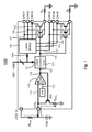
Fig. 1 shows schematically a gate pulse modulation (GPM) circuit according to one embodiment of the present invention; -
Fig. 2 shows schematically a block diagram of a logic control unit utilized in the GPM circuit according to one embodiment of the present invention; -
Fig. 3 (a)-(d) show schematically current flows established at different times in the GPM as shown inFig. 1 ; -
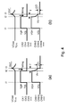
Fig. 4 (a)-(b) show schematically waveforms of the clock signals and the modulated clock signals generated by the GPM circuit according to one embodiment of the present invention, (a) odd channels, and (b) even channels; -
Fig. 5 shows schematically waveforms of a clock signal, a level-shifted clock signal and a modulated clock signal generated by the GPM circuit according to one embodiment of the present invention; -
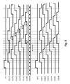
Fig. 6 shows schematically waveforms of clock signals and modulated clock signals generated by the GPM circuit according to one embodiment of the present invention; -
Fig. 7 shows schematically a block diagram of an LCD according to one embodiment of the present invention; and -
Fig. 8 shows schematically a GPM circuit and a shift register utilized in an LCD according to one embodiment of the present invention. - The present invention is more particularly described in the following examples that are intended as illustrative only since numerous modifications and variations therein will be apparent to those skilled in the art. Various embodiments of the invention are now described in detail. Referring to the drawings, like numbers indicate like components throughout the views. As used in the description herein and throughout the claims that follow, the meaning of "a", "an", and "the" includes plural reference unless the context clearly dictates otherwise. Also, as used in the description herein and throughout the claims that follow, the meaning of "in" includes "in" and "on" unless the context clearly dictates otherwise.
- The terms used in this specification generally have their ordinary meanings in the art, within the context of the invention, and in the specific context where each term is used. Certain terms that are used to describe the invention are discussed below, or elsewhere in the specification, to provide additional guidance to the practitioner regarding the description of the invention. The use of examples anywhere in this specification, including examples of any terms discussed herein, is illustrative only, and in no way limits the scope and meaning of the invention or of any exemplified term. Likewise, the invention is not limited to various embodiments given in this specification.
- As used herein, "around", "about" or "approximately" shall generally mean within 20 percent, preferably within 10 percent, and more preferably within 5 percent of a given value or range. Numerical quantities given herein are approximate, meaning that the term "around", "about" or "approximately" can be inferred if not expressly stated.
- As used herein, the terms "comprise or comprising", "include or including", "have or having", "contain or containing" and the like are to be understood to be open-ended, i.e., to mean including but not limited to.
- The description will be made as to the embodiments of the present invention in conjunction with the accompanying drawings in
Figs. 1-8 . In accordance with the purposes of this invention, as embodied and broadly described herein, this invention, in one aspect, relates to a gate pulse modulation (GPM) circuit usable in a liquid crystal display (LCD). - Referring to
Fig. 1 , aGPM circuit 100 is shown according to one embodiment of the present invention. TheGPM circuit 100 includes a low dropout (LDO) regulator LDO_O, a capacitor Cset, a first resistor RCset, a second resistor RDTS, and a fourth resistor RE, a third resistor RO, a switch device SW, acomparator 110, alogic control unit 120, alevel shifter 130, and N switches {Sj}, j = 1, 2, 3, ...N, N being an even integer greater than zero. In this exemplary embodiment as shown inFig. 1 , N = 6, i.e., a six-phase configuration is shown. In one embodiment, the LDO regulator LDO_0 is a current source. - As shown in
Fig. 1 , the first resistor RCset has a first terminal electrically connected to the LDO regulator LDO_O and a second terminal electrically connected to a node DTS, respectively. The capacitor Cset has a first terminal electrically connected to the second terminal of the first resistor RCset and a second terminal electrically connected to the ground, respectively. The switch device SW has a control terminal, a first terminal electrically connected to the node DTS, and a second terminal. The second resistor RDTS has a first terminal electrically connected to the second terminal of the switch SW and a second terminal electrically connected to the ground, respectively. - The
comparator 110 has afirst input 111 electrically connected to the node DTS, asecond input 112 for receiving a voltage signal Vref, and anoutput 113 electrically connected to the control terminal of the switch device SW, respectively. - The
level shifter 130 is adapted for converting voltage levels of one or more clock signals into desired voltage levels. In the six-phase configuration, as shown inFig. 1 , thelevel shifter 130 has aninput port 130a (or six (6) inputs) for receiving six (6) clock signals CK1, CK2, ..., CK6, and six (6) outputs 131, 132, ..., 136 for outputting six corresponding level-shitted clock signals LS1, LS2, ..., LS6, respectively. These clock signals CK1, CK2, ..., CK6 are usually generated by a time controller TCON. The level-shitted clock signals LS1, LS2, ..., LS6 are modulated by theGPM circuit 100 in the form of modulated clock signals CKH1, CKH2, ..., CKH6, respectively. - For example, as shown in
Fig. 5 , each of the clock signals CK1, CK2, ..., CK6 has a rectangle waveform with a low voltage, 0V, and a high voltage, 2.5V. After the clock signals CK1, CK2, ..., CK6 are level-shifted by the level shifter, the corresponding level-shifted clock signals LS1, LS2, ..., LS6 has the same waveform as that of the clock signals CK1, CK2, ..., CK6, but with the low voltage shifted to -7V and the high voltage shifted to 23V, respectively. Each of the clock signals CK1, CK2, ..., CK6 and the level-shifted clock signals LS1, LS2, ..., LS6 has a falling edge. According to the present invention, the level-shifted clock signals LS1, LS2, ..., LS6 are respectively modulated via a predetermined discharging process as will be discussed below, such that each of the corresponding modulated clock signals CKH1, CKH2, ..., CKH6 has a waveform with a desired slope edge. Further, the slope rate for the odd modulated clock signals CKH1, CKH3, CKH5 is different from that for the even modulated clock signals CKH2, CKH4, CKH6. - Referring back to
Fig. 1 , thelogic control unit 120 has afirst input port 121 for receiving six (6) clock signals CK1, CK2, ..., CK6, asecond input 122 is electrically connected to theoutput 113 of thecomparator 110 and anoutput 126. - As shown in
Fig. 1 , in the six-phase configuration, theGPM circuit 100 includes six switches S1, S2, ..., S6. Each switch has a control terminal electrically connected to theoutput 126 of thelogic control unit 120, a first terminal is electrically connected to arespective output 131/132/.../136 of thelevel shifter 130, and a second terminal. For the odd switches S1, S3, S5, their second terminals are electrically connected to the first terminal of the third resistor RO, which its second terminal is electrically connected to the ground. For the even switches S2, S4, S6, their second terminals are electrically connected to the first terminal of the fourth resistor RE, which its second terminal is electrically connected to the ground. - For such a configuration of the GPM circuit, as shown in
Fig. 4 , each modulated clock signal CKH1/CKH2/.../CKH6 has a waveform that rises from a first voltage VGL into a second voltage VGH at time t1, remains at the second voltage VGH until time t2, falls from the second voltage VGH at time t2 into a third voltage Vj at time t3 at a desired slope and falls from the third voltage Vj into the first voltage VGL at time t3. T = (t3 - t2) defines a falling time of each modulated clock signal CKH1/CKH2/.../CKH6, which is a function of the capacitance of the capacitor Cset. The third voltage Vk of the waveform of each odd modulated clock signal CKH1/CKH3/CKH5 is a function of the resistance of the third resistor RO, while the third voltage Vq of the waveform of each even modulated clock signal CKH2/CKH4/CKH6 is a function of the resistance of the fourth resistor RE. In other words, the voltage difference ΔV1 = (Vk - VGL) between the third voltage Vk and the first voltage VGL of the waveform of each odd modulated clock signal CKH1/CKH3/CKH5 is a function of the resistance of the third resistor RO, and the voltage difference ΔV2 = (Vq - VGL) between the third voltage Vq and the first voltage VGL of the waveform of each even modulated clock signal CKH2/CKH4/CKH6 is a function of the resistance of the fourth resistor RE. Therefore, according to the present invention, ΔV1 and ΔV2 can have different values by choosing the resistance of the third resistor RO different from the resistance of the fourth resistor RE. - Referring to
Fig. 2 , thelogic control unit 120 has a CK pulse fallingedge detector 123, acomparator output detector 124 and a switch ON/OFF controller 125. The CK pulse fallingedge detector 123 is adapted for receiving each of the N clock signals {CKj}, j = 1, 2, 3, ..., N, generated from thetime controller TCON 101, and for detecting a falling edge of a waveform of each of the received N clock signals {CKj}. Thecomparator output detector 124 is adapted for receiving an output signal output from thecomparator 110. The switch ON/OFF controller 125 in communications with the CK pulse fallingedge detector 123 and thecomparator output detector 124 is adapted for generating a signal to turn on or turn off a corresponding switch of the N switches {Sj}, j = 1, 2, 3, ..., N, in accordance with the detected falling edge of the corresponding modulated clock signal by the CK pulse fallingedge detector 123 and the detected output signal from the comparator by thecomparator output detector 124. - Specifically, when the CK pulse falling
edge detector 123 detects a falling edge at time t2 in the first clock signal CK1, where its voltage level falls from a high voltage VgH to a low voltage VgL, as shown inFig. 4(a) , the switch ON/OFF controller 125 responsively generates a first signal to turn on the corresponding switch S1. Accordingly, a current ICKH1 flows from theoutput 131 of thelevel shifter 130 through the third resistor RO to the ground, as shown inFig. 3(b) , which discharges the corresponding level-shifted clock signal LS1, thereby causing the modulated clock signal CKH1 to decrease from the second voltage VGH with a falling slope. Meanwhile, the LDO regulator LDO_O provides a current signal I1 passing through the first resistor RCset to charge the capacitor Cset, thereby charging the node DTS to have a voltage VDTS as shown inFig. 3(a) . - Then, the
comparator 110 compares the voltage VDTS of the DTS node with the reference voltage Vref. When VDTS = Vref at time t3, as shown inFig. 4(a) , thecomparator 110 generates an output signal to thecomparator output detector 124 to cause the switch ON/OFF controller 125 to generate a second signal to turn off the corresponding switch S1, as shown inFig. 3(d) , where no current flows from theoutput 131 of thelevel shifter 130 through the third resistor RO to the ground. Accordingly, the modulated clock signal CKH1 decreases to the third level Vk at time t3, as shown inFig. 4(a) . Meanwhile, the generated output signal is applied to the control terminal of the switch device SW to turn on the switch device SW, so that a current I2 flows from the node DTS through the second resistor RDTS to the ground, thereby discharging the voltage VDTS of the node DTS through the second resistor RDTS to the ground, as shown inFig. 3(c) . Preferably, the voltage VDTS of the node DTS is discharged to zero prior to the next cycle of the processes. The charging time T = (t3 - t2) of the capacitor Cset from zero to Vref is the falling slope time of the modulated clock signal CKH1 from the second voltage VGH to the third level Vk. The charging time T = (t3 - t2) of the capacitor Cset can be adjusted by setting up the voltage value of Vref. The third voltage Vk is determined by the resistance of the third resistor RO and the charging time T of the capacitor Cset. - The above processes are repeated for obtaining the other modulated clock signals, CKH2, CKH3, ..., CKH(N-1). For the even modulated clock signals CKH2, CKH4, ..., CKHN the third voltage Vq is determined by the resistance of the fourth resistor RE and the charging time T of the capacitor Cset.
-
Fig. 6 shows time charts of six clock signals CK1, CK2, ..., CK6, and the corresponding modulated clock signals CKH1, CKH2, ..., CKH6 generated from a six-phase GPM circuit according to the present invention. Each waveform of the modulated clock signals CKH1, CKH2, ..., CKH6 has a falling slope starting at the time when the waveform of the corresponding clock signal falls. -
Figs. 7 and8 show anLCD 700 that utilizes aGPM circuit 720 to modulate odd gate pulse waveforms and even gate pulse waveforms according to one embodiment of the present invention. - The
LCD 700 has anLCD panel 710 having a plurality of rows ofpixel elements pixel elements pixel elements LCD 700 also has aGPM circuit 720 for receiving four clock signals CK1, CK2, CK3 CK4, and for outputting four modulated clock signals CKH1, CKH2, CKH3, CKH4. Each modulated clock signal CKH1/CKH2/CKH3/CKH4 is corresponding to a clock signal CK1/CK2/CK3/CK4 and has a waveform having a desired falling slope. The details of theGPM circuit 720 is same as that of theGPM circuit 100, as shown inFig. 1 and discussed above, except in the embodiment, a four-phase configuration is utilized. The modulated clock signals CKH1, CKH2, CKH3, CKH4 are input to ashift register 730 formed on a glass substrate of theLCD panel 710, i.e., the gate on array (GOA). Theshift register 730 responsively generates a plurality of gate signals G(1), G(2), .... According to the present invention, the waveforms of the odd gate signals and of the even gate signals are different. When the plurality of gate signals G(1), G(2), ... is sequentially applied to the plurality of gate lines g1, g2, ... to drive the plurality of rows ofpixel elements - The foregoing description of the exemplary embodiments of the invention has been presented only for the purposes of illustration and description and is not intended to be exhaustive or to limit the invention to the precise forms disclosed. Many modifications and variations are possible in light of the above teaching.
- The embodiments were chosen and described in order to explain the principles of the invention and their practical application so as to enable others skilled in the art to utilize the invention and various embodiments and with various modifications as are suited to the particular use contemplated. Alternative embodiments will become apparent to those skilled in the art to which the present invention pertains without departing from its spirit and scope. Accordingly, the scope of the present invention is defined by the appended claims rather than the foregoing description and the exemplary embodiments described therein.
Claims (15)
- A gate pulse modulation (GPM) circuit usable in a liquid crystal display (LCD), comprising:(a) a low dropout (LDO) regulator (LDO_O);(b) a first resistor (RCset), having a first terminal electrically connected to the LDO regulator (LDO_O) and a second terminal electrically connected to a node (DTS), respectively;(c) a capacitor (Cset), having a first terminal electrically connected to the second terminal of the first resistor (RCset) and a second terminal electrically connected to the ground, respectively;(d) a switch (SW) having a control terminal, a first terminal electrically connected to the node (DTS) and a second terminal;(e) a second resistor (RDTS), having a first terminal electrically connected to the second terminal of the switch (SW) and a second terminal electrically connected to the ground, respectively;(f) a comparator having a first input electrically connected to the node (DTS), a second input for receiving a voltage signal (Vref) and an output electrically connected to the control terminal of the switch (SW), respectively;(g) a level shifter having N inputs for receiving N clock signals ({CKj}), respectively, and N outputs for outputting N modulated clock signals ({CKHj}), respectively, j = 1, 2, 3, ...N, N being an even integer greater than zero;(h) a logic control unit having a first input for receiving the N clock signals ({CKj}), a second input electrically connected to the output of the comparator and an output;(i) N switches ({Sj}), each switch (Sj) having a control terminal electrically connected to the output of the logic control unit, a first terminal electrically connected to a respective output of the level shifter, and a second terminal;(j) a third resistor (RO) having a first terminal electrically connected to the second terminal of each odd switch (Sk), k=1, 3, 5, ..., N-1, of the N switches ({Sj}) and a second terminal electrically connected to the ground, respectively; and(k) a fourth resistor (RE), having a first terminal electrically connected to the second terminal of each even switch (Sq), q =2, 4, 6, ...N, of the N switches ({Sj}) and a second terminal electrically connected to the ground, respectively.
- The GPM circuit of claim 1, wherein each modulated clock signal (CKHj) of the N modulated clock signals ({CKHj}), j = 1, 2, 3, ..., N, has a waveform that rises from a first voltage (VGL) into a second voltage (VGH) at time (t1), remains at the second voltage (VGH) until time (t2), falls from the second voltage (VGH) at time (t2) into a third voltage (Vj) at time (t3), at a desired slope and falls from the third voltage (Vj) into the first voltage (VGL) at time (t3), and wherein T = (t3 - t2) defines a falling time of each modulated clock signal (CKHj).
- The GPM circuit of claim 2, wherein the falling time T = (t3 - t2) of each modulated clock signal (CKHj), j = 1, 2, 3, ..., N, is a function of the capacitance of the capacitor (Cset).
- The GPM circuit of claim 3, wherein the third voltage (Vk) of the waveform of each odd modulated clock signal (CKHk), k = 1, 3, 5, ..., N-1, of the N modulated clock signals ({CKHj}), j = 1, 2, 3, ..., N, is a function of the resistance of the third resistor (RO), and wherein the third voltage (Vq) of the waveform of each even modulated clock signal (CKHq), q = 2, 4, 6, ..., N, of the N modulated clock signals ({CKHj}) is a function of the resistance of the fourth resistor (RE).
- The GPM circuit of claim 4, wherein the resistance of the third resistor (RO) is different from the resistance of the fourth resistor (RE), and wherein the voltage difference ΔV1 = (Vk - VGL) between the third voltage (Vk) and the first voltage (VGL) of the waveform of each odd modulated clock signal (CKHk), k = 1, 3, 5, ..., N-1, is different from the voltage difference ΔV2 = (Vq - VGL) between the third voltage (Vq) and the first voltage (VGL) of the waveform of each even modulated clock signal (CKHq), q = 2, 4, 6, ..., N.
- The GPM circuit of claim 1, wherein the logic control unit comprises:(a) a CK pulse falling edge detector for receiving each of the N clock signals ({CKj}), j = 1, 2, 3, ..., N, and detecting a falling edge of a waveform of each of the N clock signals ({CKj});(b) a comparator output detector for receiving an output signal output from the comparator; and(c) a switch ON/OFF controller in communications with the CK pulse falling edge detector and the comparator output detector for turning on or turning off a corresponding switch of the N switches ({Sj}), j = 1, 2, 3, ..., N, in accordance with the detected falling edge of the corresponding modulated clock signal by the CK pulse falling edge detector and the detected output signal from the comparator by comparator output detector.
- The GPM circuit of claim 6, wherein when the CK pulse falling edge detector detects a falling edge in a clock signal (CKj), j = 1, 2, 3, ..., N,(a) the switch ON/OFF controller responsively generates a first signal to turn on the corresponding switch (Sj), thereby discharging the corresponding modulated clock signal (CKHj) output from the j-th output of the level shifter through the third resistor (RO) or the fourth resistor (RE) to the ground; and(b) the LDO regulator (LDO_O) provides a current signal passing through the first resistor (RCset) to charge the capacitor (Cset), thereby charging the node (DTS) to have a voltage (VDTS).
- A liquid crystal display (LCD), comprising:(a) an LCD panel having a plurality of rows of pixel elements therein and a corresponding plurality of gate lines coupled to the plurality of rows of pixel elements;(b) a gate pulse modulation (GPM) circuit for receiving N clock signals ({CKj}), j =1, 2, 3, ..., N, N being an even integer greater than zero, and for outputting N modulated clock signals ({CKHj}), wherein each modulated clock signal (CKHj) is corresponding to a clock signal (CKj) and has a waveform having a desired falling slope; and(c) a shift register for receiving the N modulated clock signals ({CKHj}) and for generating a plurality of gate signals sequentially applied to the plurality of gate lines to drive the plurality of rows of pixel elements,wherein the gate pulse modulation (GPM) circuit comprises:(i) a low dropout (LDO) regulator (LDO_O);(ii) a first resistor (RCset), having a first terminal electrically connected to the LDO regulator (LDO_O) and a second terminal electrically connected to a node (DTS), respectively;(iii) a capacitor (Cset), having a first terminal electrically connected to the second terminal of the first resistor (RCset) and a second terminal electrically connected to the ground, respectively;(iv) a switch (SW), HAVING a control terminal, a first terminal electrically connected to the node (DTS) and a second terminal;(v) a second resistor (RDTS) having a first terminal electrically connected to the second terminal of the switch (SW) and a second terminal electrically connected to the ground, respectively;(vi) a comparator having a first input electrically connected to the node (DTS), a second input for receiving a voltage signal (Vref), and an output electrically connected to the control terminal of the comparator , respectively;(vii) a level shifter having N inputs for receiving the N clock signals ({CKj}), respectively, and N outputs for outputting the N modulated clock signals, ({CKHj}), respectively, j = 1, 2, 3, ...N, N being an even integer greater than zero;(viii) a logic control unit having a first input for receiving the N clock signals ({CKj}), a second input electrically connected to the output of the comparator and an output;(ix) N switches ({Sj}), each switch (Sj) having a control terminal electrically connected to the output of the logic control unit, a first terminal electrically connected to a respective output of the level shifter, and a second terminal;(x) a third resistor (RO), having a first terminal electrically connected to the second terminal of each odd switch (Sk), k=1, 3, 5, ..., N-1, of the N switches ({Sj}) and a second terminal electrically connected to the ground, respectively; and(xi) a fourth resistor (RE,) having a first terminal electrically connected to the second terminal of each even switch (Sq), q =2, 4, 6, ...N, of the N switches ({Sj}) and a second terminal electrically connected to the ground, respectively.
- The LCD of claim 8, wherein the waveform of each modulated clock signal (CKHj) of the N modulated clock signals ({CKHj}), j = 1, 2, 3, ..., N, rises from a first voltage (VGL), into a second voltage (VGH), at time( t1), remains at the second voltage (VGH) until time (t2), falls from the second voltage (VGH) at time (t2) into a third voltage (Vj) at time (t3) at a desired slope; and falls from the third voltage (Vj) into the first voltage (VGL) at time (t3), and wherein T = (t3 - t2) defines a falling time of each modulated clock signal (CKHj).
- The LCD of claim 9, wherein the falling time T = (t3 - t2) of each modulated clock signal (CKHj), j = 1, 2, 3, ..., N, is a function of the capacitance of the capacitor (Cset).
- The LCD of claim 10, wherein the third voltage (Vk) of the waveform of each odd modulated clock signal (CKHk), k = 1, 3, 5, ..., N-1, of the N modulated clock signals ({CKHj}), j = 1, 2, 3, ..., N, is a function of the resistance of the third resistor (RO), and wherein the third voltage (Vq) of the waveform of each even modulated clock signal (CKHq), q = 2, 4, 6, ..., N, of the N modulated clock signals ({CKHj}) is a function of the resistance of the fourth resistor (RE).
- The LCD of claim 11, wherein the resistance of the third resistor (RO) is different from the resistance of the fourth resistor (RE), and wherein the voltage difference ΔV1 = (Vk - VGL) between the third voltage (Vk) and the first voltage (VGL) of the waveform of each odd modulated clock signal (CKHk), k = 1, 3, 5, ..., N-1, is different from the voltage difference ΔV2 = (Vq - VGL) between the third voltage (Vq) and the first voltage (VGL) of the waveform of each even modulated clock signal (CKHq), q = 2, 4, 6, ..., N.
- The GPM circuit of claim 2 or the LCD of claim 9, wherein the corresponding clock signal (CKj) has a falling edge at time t2.
- The LCD of claim 13, wherein when the clock signal (CKj) is falling at time (t2),(c) the logic control unit generates a first signal to turn on the corresponding switch (Sj), thereby discharging the corresponding modulated clock signal (CKHj) output from the j-th output of the level shifter through the third resistor (RO) or the fourth resistor (RE) to the ground; and(d) the LDO regulator (LDO_O) provides a current signal passing through the first resistor (RCset) to charge the capacitor (Cset), thereby charging the node (DTS) to have a voltage (VDTS).
- The GPM circuit of claim 7 or the LCD of claim 14, wherein the comparator compares the voltage (VDTS) of the node (DTS) with the reference voltage (Vref), wherein when VDTS = Vref, the comparator generates an output signal to(a) the logic control unit to generate a second signal to turn off the corresponding switch (Sj); and(b) the control terminal of the switch (SW) to turn on the switch (SW), thereby discharging the voltage (VDTS) of the node (DTS) through the second resistor (RDTS) to the ground.
Applications Claiming Priority (1)
| Application Number | Priority Date | Filing Date | Title |
|---|---|---|---|
| US12/505,636 US8106873B2 (en) | 2009-07-20 | 2009-07-20 | Gate pulse modulation circuit and liquid crystal display thereof |
Publications (2)
| Publication Number | Publication Date |
|---|---|
| EP2280392A1 true EP2280392A1 (en) | 2011-02-02 |
| EP2280392B1 EP2280392B1 (en) | 2013-01-23 |
Family
ID=42148008
Family Applications (1)
| Application Number | Title | Priority Date | Filing Date |
|---|---|---|---|
| EP09180709A Active EP2280392B1 (en) | 2009-07-20 | 2009-12-23 | Gate pulse modulation circuit and liquid crystal display thereof |
Country Status (4)
| Country | Link |
|---|---|
| US (1) | US8106873B2 (en) |
| EP (1) | EP2280392B1 (en) |
| CN (1) | CN101699550B (en) |
| TW (1) | TWI416490B (en) |
Cited By (1)
| Publication number | Priority date | Publication date | Assignee | Title |
|---|---|---|---|---|
| EP2492908A3 (en) * | 2011-02-23 | 2012-11-07 | Samsung Display Co., Ltd. | Display panel and display apparatus having the same |
Families Citing this family (23)
| Publication number | Priority date | Publication date | Assignee | Title |
|---|---|---|---|---|
| MX2011008606A (en) * | 2009-03-02 | 2011-09-09 | Panasonic Corp | Base station apparatus and method of setting cell id. |
| KR20110077868A (en) * | 2009-12-30 | 2011-07-07 | 엘지디스플레이 주식회사 | Driving device of liquid crystal display |
| DE102010007351B4 (en) * | 2010-02-09 | 2018-07-12 | Texas Instruments Deutschland Gmbh | Level shifter for use in LCD display applications |
| US8988408B2 (en) * | 2010-03-22 | 2015-03-24 | Apple Inc. | Variable-bias power supply |
| CN101826315B (en) * | 2010-05-06 | 2012-06-27 | 友达光电股份有限公司 | Liquid crystal display device |
| CN101916540B (en) * | 2010-08-10 | 2012-08-29 | 友达光电股份有限公司 | Clock pulse signal generation method |
| TWI434255B (en) * | 2010-09-09 | 2014-04-11 | Au Optronics Corp | Compensation circuit of gate driving pulse signal and display device |
| TWI453722B (en) | 2011-04-12 | 2014-09-21 | Au Optronics Corp | Scan-line driving apparatus of liquid crystal display |
| TWI413094B (en) * | 2011-04-12 | 2013-10-21 | Au Optronics Corp | Half source driving display panel |
| TWI459365B (en) * | 2012-03-29 | 2014-11-01 | Ili Technology Corp | Display device and scan driver |
| CN103258514B (en) * | 2013-05-06 | 2015-05-20 | 深圳市华星光电技术有限公司 | GOA drive circuit and drive method |
| US20140340291A1 (en) * | 2013-05-14 | 2014-11-20 | Shenzhen China Star Optoelectronics Technology Co., Ltd. | Chamfered Circuit and Control Method Thereof |
| KR102142298B1 (en) | 2013-10-31 | 2020-08-07 | 주식회사 실리콘웍스 | Gate driver ic and driving method there, and control circuit of flat panel display |
| KR102263010B1 (en) | 2014-12-18 | 2021-06-09 | 주식회사 실리콘웍스 | Level shifter and display device comprising the same |
| KR102431311B1 (en) * | 2015-01-15 | 2022-08-12 | 티씨엘 차이나 스타 옵토일렉트로닉스 테크놀로지 컴퍼니 리미티드 | Display apparatus |
| KR102587318B1 (en) * | 2016-12-05 | 2023-10-12 | 티씨엘 차이나 스타 옵토일렉트로닉스 테크놀로지 컴퍼니 리미티드 | Gate driving circuit and display device having the same |
| US11164287B2 (en) | 2018-09-10 | 2021-11-02 | Lumileds Llc | Large LED array with reduced data management |
| US11107386B2 (en) * | 2018-09-10 | 2021-08-31 | Lumileds Llc | Pixel diagnostics with a bypass mode |
| US10932336B2 (en) | 2018-09-10 | 2021-02-23 | Lumileds Llc | High speed image refresh system |
| US11091087B2 (en) | 2018-09-10 | 2021-08-17 | Lumileds Llc | Adaptive headlamp system for vehicles |
| TWI826530B (en) | 2018-10-19 | 2023-12-21 | 荷蘭商露明控股公司 | Method of driving an emitter array and emitter array device |
| TWI782780B (en) * | 2021-11-05 | 2022-11-01 | 美商矽成積體電路股份有限公司 | Power management circuit in low-power double data rate memory and management method thereof |
| CN117456882A (en) * | 2023-11-13 | 2024-01-26 | 深圳市华星光电半导体显示技术有限公司 | Driving circuit, display panel and display device |
Citations (3)
| Publication number | Priority date | Publication date | Assignee | Title |
|---|---|---|---|---|
| US20060092109A1 (en) * | 2004-10-28 | 2006-05-04 | Wen-Fa Hsu | Gate driving method and circuit for liquid crystal display |
| US20070216632A1 (en) * | 2006-03-20 | 2007-09-20 | Lg.Philips Lcd Co., Ltd. | Liquid crystal display device and method of driving the same |
| US20080001887A1 (en) * | 2006-06-29 | 2008-01-03 | Lg.Philips Lcd Co., Ltd. | Circuit for generating gate pulse modulation signal and liquid crystal display device having the same |
Family Cites Families (10)
| Publication number | Priority date | Publication date | Assignee | Title |
|---|---|---|---|---|
| JP3406508B2 (en) * | 1998-03-27 | 2003-05-12 | シャープ株式会社 | Display device and display method |
| JP4371006B2 (en) * | 2004-08-17 | 2009-11-25 | セイコーエプソン株式会社 | Source driver and electro-optical device |
| KR100703463B1 (en) * | 2005-08-01 | 2007-04-03 | 삼성에스디아이 주식회사 | Data driving circuit, organic light emitting display using same and driving method thereof |
| JP5034372B2 (en) * | 2006-08-24 | 2012-09-26 | ソニー株式会社 | Level shift circuit, driving device, imaging device |
| US7557558B2 (en) * | 2007-03-19 | 2009-07-07 | Analog Devices, Inc. | Integrated circuit current reference |
| CN100460939C (en) * | 2007-04-11 | 2009-02-11 | 友达光电股份有限公司 | Liquid crystal display and its pulse adjustment circuit |
| KR100889528B1 (en) * | 2007-06-27 | 2009-03-19 | 삼성에스디아이 주식회사 | Soft-Start Circuit and Power Supply Containing It |
| KR100906103B1 (en) * | 2007-12-31 | 2009-07-07 | 엘지디스플레이 주식회사 | Array Board for Liquid Crystal Display |
| CN101315749B (en) * | 2008-06-26 | 2010-06-16 | 上海广电光电子有限公司 | Driving method of liquid crystal display |
| US8294292B2 (en) * | 2009-04-22 | 2012-10-23 | Rain Bird Corporation | Power supply system |
-
2009
- 2009-07-20 US US12/505,636 patent/US8106873B2/en active Active
- 2009-09-25 TW TW098132593A patent/TWI416490B/en active
- 2009-10-30 CN CN2009102094267A patent/CN101699550B/en active Active
- 2009-12-23 EP EP09180709A patent/EP2280392B1/en active Active
Patent Citations (3)
| Publication number | Priority date | Publication date | Assignee | Title |
|---|---|---|---|---|
| US20060092109A1 (en) * | 2004-10-28 | 2006-05-04 | Wen-Fa Hsu | Gate driving method and circuit for liquid crystal display |
| US20070216632A1 (en) * | 2006-03-20 | 2007-09-20 | Lg.Philips Lcd Co., Ltd. | Liquid crystal display device and method of driving the same |
| US20080001887A1 (en) * | 2006-06-29 | 2008-01-03 | Lg.Philips Lcd Co., Ltd. | Circuit for generating gate pulse modulation signal and liquid crystal display device having the same |
Cited By (2)
| Publication number | Priority date | Publication date | Assignee | Title |
|---|---|---|---|---|
| EP2492908A3 (en) * | 2011-02-23 | 2012-11-07 | Samsung Display Co., Ltd. | Display panel and display apparatus having the same |
| US9082362B2 (en) | 2011-02-23 | 2015-07-14 | Samsung Display Co., Ltd. | Display panel and display apparatus having the same |
Also Published As
| Publication number | Publication date |
|---|---|
| EP2280392B1 (en) | 2013-01-23 |
| CN101699550B (en) | 2012-05-23 |
| CN101699550A (en) | 2010-04-28 |
| US20110012891A1 (en) | 2011-01-20 |
| TWI416490B (en) | 2013-11-21 |
| US8106873B2 (en) | 2012-01-31 |
| TW201104662A (en) | 2011-02-01 |
Similar Documents
| Publication | Publication Date | Title |
|---|---|---|
| EP2280392B1 (en) | Gate pulse modulation circuit and liquid crystal display thereof | |
| US7403185B2 (en) | Liquid crystal display device and method of driving the same | |
| US8154500B2 (en) | Gate driver and method of driving display apparatus having the same | |
| CN101191923B (en) | Liquid crystal display system capable of improving display quality and related driving method | |
| US10049634B2 (en) | Pixel circuit and driving method thereof, driving circuit, display device | |
| CN101587700B (en) | Liquid crystal display and method for driving liquid crystal display | |
| US20070268225A1 (en) | Display device, driving apparatus for display device, and driving method of display device | |
| US8289273B2 (en) | Scan line driving circuit, electro-optical device, and electronic apparatus | |
| US8605126B2 (en) | Display apparatus | |
| KR20120082671A (en) | Device for generating gamma, lcd and method for driving the lcd | |
| CN112509528B (en) | Gate drive circuit, display device and gate drive method of display panel | |
| KR20050014116A (en) | Liquid crystal display device and driving method of the same | |
| US20120127142A1 (en) | Liquid crystal display and inversion driving method | |
| CN110827772B (en) | Display device and method of driving the same | |
| US20100085336A1 (en) | Driving unit and display apparatus having the same | |
| US20080049002A1 (en) | Scan line driving method | |
| TW201308302A (en) | Operating method and display panel using the same | |
| CN101458915A (en) | Liquid crystal display panel driving method | |
| KR20080054658A (en) | Driving device of liquid crystal display and driving method thereof | |
| TWI410939B (en) | Liquid display panel driving method | |
| US20130321367A1 (en) | Display device | |
| KR100927014B1 (en) | LCD and its driving method | |
| KR100825424B1 (en) | DSD LC drive method and driving device | |
| US8040314B2 (en) | Driving apparatus for liquid crystal display | |
| KR20070120351A (en) | Signal control device and liquid crystal display including the same |
Legal Events
| Date | Code | Title | Description |
|---|---|---|---|
| PUAI | Public reference made under article 153(3) epc to a published international application that has entered the european phase |
Free format text: ORIGINAL CODE: 0009012 |
|
| 17P | Request for examination filed |
Effective date: 20100122 |
|
| AK | Designated contracting states |
Kind code of ref document: A1 Designated state(s): AT BE BG CH CY CZ DE DK EE ES FI FR GB GR HR HU IE IS IT LI LT LU LV MC MK MT NL NO PL PT RO SE SI SK SM TR |
|
| AX | Request for extension of the european patent |
Extension state: AL BA RS |
|
| RIC1 | Information provided on ipc code assigned before grant |
Ipc: G09G 3/36 20060101AFI20110421BHEP |
|
| 17Q | First examination report despatched |
Effective date: 20110901 |
|
| GRAP | Despatch of communication of intention to grant a patent |
Free format text: ORIGINAL CODE: EPIDOSNIGR1 |
|
| GRAS | Grant fee paid |
Free format text: ORIGINAL CODE: EPIDOSNIGR3 |
|
| GRAA | (expected) grant |
Free format text: ORIGINAL CODE: 0009210 |
|
| AK | Designated contracting states |
Kind code of ref document: B1 Designated state(s): AT BE BG CH CY CZ DE DK EE ES FI FR GB GR HR HU IE IS IT LI LT LU LV MC MK MT NL NO PL PT RO SE SI SK SM TR |
|
| REG | Reference to a national code |
Ref country code: GB Ref legal event code: FG4D |
|
| REG | Reference to a national code |
Ref country code: CH Ref legal event code: EP |
|
| REG | Reference to a national code |
Ref country code: AT Ref legal event code: REF Ref document number: 595330 Country of ref document: AT Kind code of ref document: T Effective date: 20130215 Ref country code: CH Ref legal event code: EP |
|
| REG | Reference to a national code |
Ref country code: IE Ref legal event code: FG4D |
|
| REG | Reference to a national code |
Ref country code: DE Ref legal event code: R096 Ref document number: 602009012971 Country of ref document: DE Effective date: 20130321 |
|
| REG | Reference to a national code |
Ref country code: AT Ref legal event code: MK05 Ref document number: 595330 Country of ref document: AT Kind code of ref document: T Effective date: 20130123 |
|
| REG | Reference to a national code |
Ref country code: LT Ref legal event code: MG4D |
|
| REG | Reference to a national code |
Ref country code: NL Ref legal event code: VDEP Effective date: 20130123 |
|
| PG25 | Lapsed in a contracting state [announced via postgrant information from national office to epo] |
Ref country code: IS Free format text: LAPSE BECAUSE OF FAILURE TO SUBMIT A TRANSLATION OF THE DESCRIPTION OR TO PAY THE FEE WITHIN THE PRESCRIBED TIME-LIMIT Effective date: 20130523 Ref country code: BG Free format text: LAPSE BECAUSE OF FAILURE TO SUBMIT A TRANSLATION OF THE DESCRIPTION OR TO PAY THE FEE WITHIN THE PRESCRIBED TIME-LIMIT Effective date: 20130423 Ref country code: ES Free format text: LAPSE BECAUSE OF FAILURE TO SUBMIT A TRANSLATION OF THE DESCRIPTION OR TO PAY THE FEE WITHIN THE PRESCRIBED TIME-LIMIT Effective date: 20130504 Ref country code: SE Free format text: LAPSE BECAUSE OF FAILURE TO SUBMIT A TRANSLATION OF THE DESCRIPTION OR TO PAY THE FEE WITHIN THE PRESCRIBED TIME-LIMIT Effective date: 20130123 Ref country code: NO Free format text: LAPSE BECAUSE OF FAILURE TO SUBMIT A TRANSLATION OF THE DESCRIPTION OR TO PAY THE FEE WITHIN THE PRESCRIBED TIME-LIMIT Effective date: 20130423 Ref country code: LT Free format text: LAPSE BECAUSE OF FAILURE TO SUBMIT A TRANSLATION OF THE DESCRIPTION OR TO PAY THE FEE WITHIN THE PRESCRIBED TIME-LIMIT Effective date: 20130123 Ref country code: AT Free format text: LAPSE BECAUSE OF FAILURE TO SUBMIT A TRANSLATION OF THE DESCRIPTION OR TO PAY THE FEE WITHIN THE PRESCRIBED TIME-LIMIT Effective date: 20130123 Ref country code: BE Free format text: LAPSE BECAUSE OF FAILURE TO SUBMIT A TRANSLATION OF THE DESCRIPTION OR TO PAY THE FEE WITHIN THE PRESCRIBED TIME-LIMIT Effective date: 20130123 |
|
| PG25 | Lapsed in a contracting state [announced via postgrant information from national office to epo] |
Ref country code: PL Free format text: LAPSE BECAUSE OF FAILURE TO SUBMIT A TRANSLATION OF THE DESCRIPTION OR TO PAY THE FEE WITHIN THE PRESCRIBED TIME-LIMIT Effective date: 20130123 Ref country code: GR Free format text: LAPSE BECAUSE OF FAILURE TO SUBMIT A TRANSLATION OF THE DESCRIPTION OR TO PAY THE FEE WITHIN THE PRESCRIBED TIME-LIMIT Effective date: 20130424 Ref country code: LV Free format text: LAPSE BECAUSE OF FAILURE TO SUBMIT A TRANSLATION OF THE DESCRIPTION OR TO PAY THE FEE WITHIN THE PRESCRIBED TIME-LIMIT Effective date: 20130123 Ref country code: FI Free format text: LAPSE BECAUSE OF FAILURE TO SUBMIT A TRANSLATION OF THE DESCRIPTION OR TO PAY THE FEE WITHIN THE PRESCRIBED TIME-LIMIT Effective date: 20130123 Ref country code: NL Free format text: LAPSE BECAUSE OF FAILURE TO SUBMIT A TRANSLATION OF THE DESCRIPTION OR TO PAY THE FEE WITHIN THE PRESCRIBED TIME-LIMIT Effective date: 20130123 Ref country code: SI Free format text: LAPSE BECAUSE OF FAILURE TO SUBMIT A TRANSLATION OF THE DESCRIPTION OR TO PAY THE FEE WITHIN THE PRESCRIBED TIME-LIMIT Effective date: 20130123 Ref country code: PT Free format text: LAPSE BECAUSE OF FAILURE TO SUBMIT A TRANSLATION OF THE DESCRIPTION OR TO PAY THE FEE WITHIN THE PRESCRIBED TIME-LIMIT Effective date: 20130523 |
|
| PG25 | Lapsed in a contracting state [announced via postgrant information from national office to epo] |
Ref country code: HR Free format text: LAPSE BECAUSE OF FAILURE TO SUBMIT A TRANSLATION OF THE DESCRIPTION OR TO PAY THE FEE WITHIN THE PRESCRIBED TIME-LIMIT Effective date: 20130123 |
|
| PG25 | Lapsed in a contracting state [announced via postgrant information from national office to epo] |
Ref country code: CZ Free format text: LAPSE BECAUSE OF FAILURE TO SUBMIT A TRANSLATION OF THE DESCRIPTION OR TO PAY THE FEE WITHIN THE PRESCRIBED TIME-LIMIT Effective date: 20130123 Ref country code: EE Free format text: LAPSE BECAUSE OF FAILURE TO SUBMIT A TRANSLATION OF THE DESCRIPTION OR TO PAY THE FEE WITHIN THE PRESCRIBED TIME-LIMIT Effective date: 20130123 Ref country code: SK Free format text: LAPSE BECAUSE OF FAILURE TO SUBMIT A TRANSLATION OF THE DESCRIPTION OR TO PAY THE FEE WITHIN THE PRESCRIBED TIME-LIMIT Effective date: 20130123 Ref country code: RO Free format text: LAPSE BECAUSE OF FAILURE TO SUBMIT A TRANSLATION OF THE DESCRIPTION OR TO PAY THE FEE WITHIN THE PRESCRIBED TIME-LIMIT Effective date: 20130123 Ref country code: DK Free format text: LAPSE BECAUSE OF FAILURE TO SUBMIT A TRANSLATION OF THE DESCRIPTION OR TO PAY THE FEE WITHIN THE PRESCRIBED TIME-LIMIT Effective date: 20130123 |
|
| PG25 | Lapsed in a contracting state [announced via postgrant information from national office to epo] |
Ref country code: CY Free format text: LAPSE BECAUSE OF FAILURE TO SUBMIT A TRANSLATION OF THE DESCRIPTION OR TO PAY THE FEE WITHIN THE PRESCRIBED TIME-LIMIT Effective date: 20130123 |
|
| PLBE | No opposition filed within time limit |
Free format text: ORIGINAL CODE: 0009261 |
|
| STAA | Information on the status of an ep patent application or granted ep patent |
Free format text: STATUS: NO OPPOSITION FILED WITHIN TIME LIMIT |
|
| PG25 | Lapsed in a contracting state [announced via postgrant information from national office to epo] |
Ref country code: IT Free format text: LAPSE BECAUSE OF FAILURE TO SUBMIT A TRANSLATION OF THE DESCRIPTION OR TO PAY THE FEE WITHIN THE PRESCRIBED TIME-LIMIT Effective date: 20130123 |
|
| 26N | No opposition filed |
Effective date: 20131024 |
|
| REG | Reference to a national code |
Ref country code: DE Ref legal event code: R097 Ref document number: 602009012971 Country of ref document: DE Effective date: 20131024 |
|
| PG25 | Lapsed in a contracting state [announced via postgrant information from national office to epo] |
Ref country code: MC Free format text: LAPSE BECAUSE OF FAILURE TO SUBMIT A TRANSLATION OF THE DESCRIPTION OR TO PAY THE FEE WITHIN THE PRESCRIBED TIME-LIMIT Effective date: 20130123 |
|
| REG | Reference to a national code |
Ref country code: CH Ref legal event code: PL |
|
| PG25 | Lapsed in a contracting state [announced via postgrant information from national office to epo] |
Ref country code: LU Free format text: LAPSE BECAUSE OF FAILURE TO SUBMIT A TRANSLATION OF THE DESCRIPTION OR TO PAY THE FEE WITHIN THE PRESCRIBED TIME-LIMIT Effective date: 20131223 |
|
| REG | Reference to a national code |
Ref country code: IE Ref legal event code: MM4A |
|
| PG25 | Lapsed in a contracting state [announced via postgrant information from national office to epo] |
Ref country code: LI Free format text: LAPSE BECAUSE OF NON-PAYMENT OF DUE FEES Effective date: 20131231 Ref country code: CH Free format text: LAPSE BECAUSE OF NON-PAYMENT OF DUE FEES Effective date: 20131231 Ref country code: IE Free format text: LAPSE BECAUSE OF NON-PAYMENT OF DUE FEES Effective date: 20131223 |
|
| PG25 | Lapsed in a contracting state [announced via postgrant information from national office to epo] |
Ref country code: SM Free format text: LAPSE BECAUSE OF FAILURE TO SUBMIT A TRANSLATION OF THE DESCRIPTION OR TO PAY THE FEE WITHIN THE PRESCRIBED TIME-LIMIT Effective date: 20130123 |
|
| PG25 | Lapsed in a contracting state [announced via postgrant information from national office to epo] |
Ref country code: TR Free format text: LAPSE BECAUSE OF FAILURE TO SUBMIT A TRANSLATION OF THE DESCRIPTION OR TO PAY THE FEE WITHIN THE PRESCRIBED TIME-LIMIT Effective date: 20130123 |
|
| PG25 | Lapsed in a contracting state [announced via postgrant information from national office to epo] |
Ref country code: HU Free format text: LAPSE BECAUSE OF FAILURE TO SUBMIT A TRANSLATION OF THE DESCRIPTION OR TO PAY THE FEE WITHIN THE PRESCRIBED TIME-LIMIT; INVALID AB INITIO Effective date: 20091223 Ref country code: MK Free format text: LAPSE BECAUSE OF FAILURE TO SUBMIT A TRANSLATION OF THE DESCRIPTION OR TO PAY THE FEE WITHIN THE PRESCRIBED TIME-LIMIT Effective date: 20130123 |
|
| PG25 | Lapsed in a contracting state [announced via postgrant information from national office to epo] |
Ref country code: MT Free format text: LAPSE BECAUSE OF FAILURE TO SUBMIT A TRANSLATION OF THE DESCRIPTION OR TO PAY THE FEE WITHIN THE PRESCRIBED TIME-LIMIT Effective date: 20130123 |
|
| REG | Reference to a national code |
Ref country code: FR Ref legal event code: PLFP Year of fee payment: 7 |
|
| REG | Reference to a national code |
Ref country code: FR Ref legal event code: PLFP Year of fee payment: 8 |
|
| REG | Reference to a national code |
Ref country code: FR Ref legal event code: PLFP Year of fee payment: 9 |
|
| PGFP | Annual fee paid to national office [announced via postgrant information from national office to epo] |
Ref country code: DE Payment date: 20251104 Year of fee payment: 17 |
|
| PGFP | Annual fee paid to national office [announced via postgrant information from national office to epo] |
Ref country code: GB Payment date: 20251030 Year of fee payment: 17 |
|
| PGFP | Annual fee paid to national office [announced via postgrant information from national office to epo] |
Ref country code: FR Payment date: 20251110 Year of fee payment: 17 |