EP2277211B1 - Manufacturing method of a magnetic tunnel junction element using two masks - Google Patents
Manufacturing method of a magnetic tunnel junction element using two masks Download PDFInfo
- Publication number
- EP2277211B1 EP2277211B1 EP09732874.4A EP09732874A EP2277211B1 EP 2277211 B1 EP2277211 B1 EP 2277211B1 EP 09732874 A EP09732874 A EP 09732874A EP 2277211 B1 EP2277211 B1 EP 2277211B1
- Authority
- EP
- European Patent Office
- Prior art keywords
- electrode
- mtj
- mask
- layer
- magnetic
- Prior art date
- Legal status (The legal status is an assumption and is not a legal conclusion. Google has not performed a legal analysis and makes no representation as to the accuracy of the status listed.)
- Not-in-force
Links
- 230000005291 magnetic effect Effects 0.000 title claims description 49
- 238000004519 manufacturing process Methods 0.000 title description 19
- 238000000034 method Methods 0.000 claims description 58
- 230000004888 barrier function Effects 0.000 claims description 33
- 238000001465 metallisation Methods 0.000 claims description 25
- 238000002161 passivation Methods 0.000 claims description 16
- 238000000151 deposition Methods 0.000 claims description 10
- 238000004891 communication Methods 0.000 claims description 8
- 229910052751 metal Inorganic materials 0.000 claims description 8
- 239000002184 metal Substances 0.000 claims description 8
- 239000000758 substrate Substances 0.000 claims description 4
- 230000008569 process Effects 0.000 description 35
- 238000013461 design Methods 0.000 description 19
- 230000008901 benefit Effects 0.000 description 9
- 238000003860 storage Methods 0.000 description 9
- 239000004065 semiconductor Substances 0.000 description 8
- 230000010354 integration Effects 0.000 description 6
- 229910052715 tantalum Inorganic materials 0.000 description 5
- GUVRBAGPIYLISA-UHFFFAOYSA-N tantalum atom Chemical compound [Ta] GUVRBAGPIYLISA-UHFFFAOYSA-N 0.000 description 5
- RYGMFSIKBFXOCR-UHFFFAOYSA-N Copper Chemical compound [Cu] RYGMFSIKBFXOCR-UHFFFAOYSA-N 0.000 description 4
- 229910052802 copper Inorganic materials 0.000 description 4
- 239000010949 copper Substances 0.000 description 4
- 230000008878 coupling Effects 0.000 description 4
- 238000010168 coupling process Methods 0.000 description 4
- 238000005859 coupling reaction Methods 0.000 description 4
- 238000010586 diagram Methods 0.000 description 4
- 230000015572 biosynthetic process Effects 0.000 description 3
- 239000012212 insulator Substances 0.000 description 3
- 239000000463 material Substances 0.000 description 3
- 150000002739 metals Chemical class 0.000 description 3
- 239000000203 mixture Substances 0.000 description 3
- 238000005498 polishing Methods 0.000 description 3
- 238000012545 processing Methods 0.000 description 3
- 230000005290 antiferromagnetic effect Effects 0.000 description 2
- 238000009792 diffusion process Methods 0.000 description 2
- 230000006870 function Effects 0.000 description 2
- 239000000696 magnetic material Substances 0.000 description 2
- 229910044991 metal oxide Inorganic materials 0.000 description 2
- 150000004706 metal oxides Chemical class 0.000 description 2
- 238000000059 patterning Methods 0.000 description 2
- 230000002093 peripheral effect Effects 0.000 description 2
- 239000003870 refractory metal Substances 0.000 description 2
- HBMJWWWQQXIZIP-UHFFFAOYSA-N silicon carbide Chemical compound [Si+]#[C-] HBMJWWWQQXIZIP-UHFFFAOYSA-N 0.000 description 2
- 229910010271 silicon carbide Inorganic materials 0.000 description 2
- 238000012546 transfer Methods 0.000 description 2
- 241000283283 Orcinus orca Species 0.000 description 1
- 229910052581 Si3N4 Inorganic materials 0.000 description 1
- 229910004541 SiN Inorganic materials 0.000 description 1
- VYPSYNLAJGMNEJ-UHFFFAOYSA-N Silicium dioxide Chemical compound O=[Si]=O VYPSYNLAJGMNEJ-UHFFFAOYSA-N 0.000 description 1
- XUIMIQQOPSSXEZ-UHFFFAOYSA-N Silicon Chemical compound [Si] XUIMIQQOPSSXEZ-UHFFFAOYSA-N 0.000 description 1
- 230000004075 alteration Effects 0.000 description 1
- 230000000903 blocking effect Effects 0.000 description 1
- 230000008859 change Effects 0.000 description 1
- 230000000295 complement effect Effects 0.000 description 1
- 238000010276 construction Methods 0.000 description 1
- -1 copper Chemical class 0.000 description 1
- 230000003247 decreasing effect Effects 0.000 description 1
- 230000000694 effects Effects 0.000 description 1
- 238000000609 electron-beam lithography Methods 0.000 description 1
- 230000008030 elimination Effects 0.000 description 1
- 238000003379 elimination reaction Methods 0.000 description 1
- 238000005516 engineering process Methods 0.000 description 1
- 230000005294 ferromagnetic effect Effects 0.000 description 1
- 230000006872 improvement Effects 0.000 description 1
- 230000005415 magnetization Effects 0.000 description 1
- 150000001247 metal acetylides Chemical class 0.000 description 1
- 229910003465 moissanite Inorganic materials 0.000 description 1
- 150000004767 nitrides Chemical class 0.000 description 1
- 230000008520 organization Effects 0.000 description 1
- 230000035515 penetration Effects 0.000 description 1
- 238000000206 photolithography Methods 0.000 description 1
- 230000010287 polarization Effects 0.000 description 1
- 230000009467 reduction Effects 0.000 description 1
- 229910052710 silicon Inorganic materials 0.000 description 1
- 239000010703 silicon Substances 0.000 description 1
- HQVNEWCFYHHQES-UHFFFAOYSA-N silicon nitride Chemical compound N12[Si]34N5[Si]62N3[Si]51N64 HQVNEWCFYHHQES-UHFFFAOYSA-N 0.000 description 1
- 229910052814 silicon oxide Inorganic materials 0.000 description 1
- 238000004088 simulation Methods 0.000 description 1
- 125000006850 spacer group Chemical group 0.000 description 1
- 241000894007 species Species 0.000 description 1
- 239000000126 substance Substances 0.000 description 1
- 238000006467 substitution reaction Methods 0.000 description 1
- 230000005641 tunneling Effects 0.000 description 1
- 238000012795 verification Methods 0.000 description 1
Images

Classifications
-
- G—PHYSICS
- G11—INFORMATION STORAGE
- G11C—STATIC STORES
- G11C11/00—Digital stores characterised by the use of particular electric or magnetic storage elements; Storage elements therefor
- G11C11/02—Digital stores characterised by the use of particular electric or magnetic storage elements; Storage elements therefor using magnetic elements
- G11C11/16—Digital stores characterised by the use of particular electric or magnetic storage elements; Storage elements therefor using magnetic elements using elements in which the storage effect is based on magnetic spin effect
- G11C11/161—Digital stores characterised by the use of particular electric or magnetic storage elements; Storage elements therefor using magnetic elements using elements in which the storage effect is based on magnetic spin effect details concerning the memory cell structure, e.g. the layers of the ferromagnetic memory cell
-
- H—ELECTRICITY
- H10—SEMICONDUCTOR DEVICES; ELECTRIC SOLID-STATE DEVICES NOT OTHERWISE PROVIDED FOR
- H10N—ELECTRIC SOLID-STATE DEVICES NOT OTHERWISE PROVIDED FOR
- H10N50/00—Galvanomagnetic devices
- H10N50/01—Manufacture or treatment
-
- H—ELECTRICITY
- H10—SEMICONDUCTOR DEVICES; ELECTRIC SOLID-STATE DEVICES NOT OTHERWISE PROVIDED FOR
- H10N—ELECTRIC SOLID-STATE DEVICES NOT OTHERWISE PROVIDED FOR
- H10N50/00—Galvanomagnetic devices
- H10N50/10—Magnetoresistive devices
Definitions
- This disclosure relates to methods of integration of magnetic random access memory, and in particular, to spin torque transfer magnetic random access memory, with standard integrated circuit fabrication processes.
- MRAM magnetic RAM
- data is not stored as electric charge, but is instead stored by magnetic polarization of a storage element - a magnetic tunnel junction, i.e., an MTJ.
- the elements are formed from two ferromagnetic plates, each of which can hold a magnetic field, separated by a thin insulating layer.
- One of the two plates is a permanent magnet set to a particular polarity; the magnetization polarity of the other "writable" plate will change to match that of a sufficiently strong external field.
- a memory device is built from a grid of such "cells".
- Reading is accomplished by measuring the electrical resistance of the cell.
- a particular cell is conventionally selected by powering an associated transistor which switches current from a supply line through the cell to ground. Due to the tunneling magnetoresistance effect, the electrical resistance of the cell changes duc to the orientation of the fields in the two plates. By measuring the resulting current, the resistance inside any particular cell can be determined, and from this the polarity of the writable plate. Conventionally, if the two plates have the same polarity this is considered a state "0", whereas if the two plates are of opposite polarity the resistance will be higher and is considered a state "1".
- EP 1860769 describes a microwave generating element comprising a lower electrode, a layer formed on the lower electrode in an island shape, forming a magnetoresistance element, an insulator formed on the lower electrode in such a manner as to surround the layer fouling the magnetoresistance element, and an upper electrode formed on the insulator and the layer forming the magnetoresistance element.
- EP 1689006 describes a multi-bit magnetic memory device using a spin-polarized current and methods of manufacturing and operating the same.
- the magnetic memory device includes a switching device and a magnetic storage node connected to the switching device, wherein the magnetic storage node includes a first magnetic layer, a second magnetic layer and a free magnetic layer.
- US 2004/0043526 describes a method of patterning a layer of magnetic material to form isolated magnetic regions.
- the method forms a mask on a film stack comprising a layer of magnetic material such that the protected and unprotected regions are defined.
- the unprotected regions arc oxidized to form isolated magnetic regions.
- US 2005/0090056 describes a method of making a magnetic tunnel junction device.
- the magnetic tunnel junction device includes a magnetic tunnel junction stack and an electrically non-conductive spacer in contact with a portion of the magnetic tunnel junction stack.
- US-2004/0205958 describes a method for fabricating a magnetic memory element structure comprising the provision of a dielectric layer having a conducting via, forming a first magnetic layer overlying the dielectric layer, and forming a nonmagnetic layer and second magnetic layer overlying the first magnetic layer.
- a first conductive layer is deposited overlying the second magnetic layer.
- a portion of the second magnetic layer is exposed and is transformed to form an inactive portion and an active portion.
- a method is provided in accordance with claim 1, preferably a method of integrating magnetic random access memory (MRAM) fabrication processes into standard back-end-of-line (BEOL) integrated circuit manufacturing.
- MRAM magnetic random access memory
- a method for forming a magnetic tunnel junction (MTJ) device for magnetic random access memory (MRAM) using two masks includes depositing, on a substrate having a first interconnect metallization, a first electrode in communication with the first interconnect metallization, MTJ layers, and a second electrode. The method also includes defining at least some of the MTJ layers and the second electrode with a first mask; and depositing a third electrode on the second electrode. The method further includes defining the first electrode and the third electrode with a second mask larger than the first mask.
- a not claimed magnetic tunnel junction (MTJ) structure for magnetic random access memory has a substrate with a first interconnect metallization.
- the structure also includes a first electrode coupled to the first interconnect metallization, and MTJ layers. At least one of the MTJ layers is coupled to the first electrode.
- the structure further includes a second electrode coupled to at least one other of the MTJ layers, the second electrode having a same lateral dimension as at least some of the MTJ layers based upon a first mask.
- the structure additionally includes a third electrode coupled to the second electrode, the third electrode having a same lateral dimension as the first electrode based upon a second mask.
- the structure also has a second interconnect metallization coupled to the third electrode.
- a not claimed magnetic tunnel junction (MTJ) structure for magnetic random access memory includes a first interconnect means for communicating with at least one control device; a first electrode means for coupling to the first interconnect means; and an MTJ means for storing data.
- the MTJ means couples to the first electrode means.
- the structure further includes a second electrode means for coupling to the MTJ means, and a third electrode means for coupling to the second electrode means.
- the second electrode means has a same lateral dimension as the MTJ means based upon a first mask.
- the third electrode means has a same lateral dimension as the first electrode means based upon a second mask.
- the structure also has a second interconnect means for coupling to the third electrode means and at least one other control device.
- a method of forming an MTJ device are disclosed.
- a spin-torque-transfer (STT) MTJ is used.
- FIGURE 1 shows an exemplary wireless communication system 100 in which an example of the disclosure may be advantageously employed.
- FIGURE 1 shows three remote units 120, 130, and 150 and two base stations 140. It will be recognized that conventional wireless communication systems may have many more remote units and base stations.
- the remote units 120, 130, and 150 include STT MRAM devices 125A, 125B and 125C, which are an example of the disclosure as discussed further below.
- FIGURE 1 shows forward link signals 180 from the base stations 140 and the remote units 120, 130, and 150 and reverse link signals 190 from the remote units 120, 130, and 150 to the base stations 140.
- the remote unit 120 is shown as a mobile telephone
- the remote unit 130 is shown as a portable computer
- the remote unit 150 is shown as a fixed location remote unit in a wireless local loop system.
- the remote units may be mobile phones, hand-held personal communication systems (PCS) units, portable data units such as personal data assistants, navigation devices (such as GPS enabled devices), set top boxes, music players, video players, entertainment units, fixed location data units such as meter reading equipment, or any other device that stores or retrieves data or computer instructions, or any combination thereof.
- PCS personal communication systems
- FIGURE 1 illustrates remote units according to the teachings of the disclosure, the disclosure is not limited to these exemplary illustrated units.
- the disclosed device may be suitably employed in any device which includes MRAM devices.
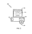
- FIGURE 2 is a block diagram illustrating a design workstation used for circuit, layout, and logic design of the disclosed semiconductor integrated circuit.
- a design workstation 200 includes a hard disk 201 containing operating system software, support files, and design software such as CADENCE or ORCAD.
- the design workstation 200 also includes a display 202 to facilitate design of a circuit design 210.
- the circuit design 210 may be the memory circuit as disclosed above.
- a storage medium 204 is provided for tangibly storing the circuit design 210.
- the circuit design 210 may be stored on the storage medium 204 in a file format such as GDSII or GERBER.
- the storage medium 204 may be a CD-ROM, DVD, hard disk, flash memory, or other appropriate device.
- the design workstation 200 includes a drive apparatus 203 for accepting input from or writing output to the storage medium 204.
- Data recorded on the storage medium 204 may specify logic circuit configurations, pattern data for photolithography masks, or mask pattern data for serial write tools such as electron beam lithography.
- the data may further include logic verification data such as timing diagrams or net circuits associated with logic simulations.
- Providing data on the storage medium 204 facilitates the design of the circuit design 210 by decreasing the number of processes for designing semiconductor ICs.
- method of making an MRAM device utilizes as little as two masks to form an MTJ.
- the method is applied substantially to making STT MRAM. This enables potentially large reductions in the cost of imbedding memory in an integrated circuit product.
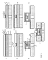
- FIGURE 3 is a schematic process flow of one embodiment of processing used to form an MTJ MRAM structure that may be imbedded in a semiconductor BEOL process.
- An interlevel dielectric, ILD 36 separates MTJ layers from peripheral devices (not shown) that have been previously fabricated in a back-end-of line (BEOL) process flow.
- An interconnect metallization 37 formed in the ILD 36 provides connection to the control devices (for example, an access transistor associated with an MTJ).
- the interconnect metallization 37 Beginning with a surface including the interconnect metallization 37 and the first ILD 36, a succession of layers are disposed on the surface, including a conductive first electrode 30, a reference fixed magnetic layer stack 32 (including a fixed antiferromagnetic layer and a synthetic antiferro-magnetic layer, neither of which are shown in FIGURE 3 ), a tunnel barrier layer 12, a free layer 11, and a second electrode 6.
- the interconnect metallization 37 connects an MTJ to a source line.
- a conventional dielectric barrier between the ILD 36 and the first contact layer 30 is absent.
- the first electrode 30 may be a refractory metal, such as, for example tantalum (Ta).
- the interconnect metallization 37 may be copper, and tantalum is an excellent barrier material for blocking diffusion of copper into surrounding materials. In other words, tantalum blocks diffusion of metals, such as copper, in the interconnect metallization 37, reducing or eliminating the need for the conventional dielectric barrier.
- depositing a tantalum layer on the ILD 36 and the interconnect metallization 37 is a process friendly integration scheme common to complementary metal oxide semiconductor (CMOS) fabrication.
- CMOS complementary metal oxide semiconductor
- a first mask process is used to etch and pattern various upper layers and electrodes, including the tunnel barrier layer 12, the free layer 11 and the second electrode 6, but not including the reference fixed magnetic layer stack 32.
- removal of a portion of and patterning the reference fixed magnetic layer stack 32 with the first mask may also take place.
- the core MTJ "stack" structure is defined, and includes the tunnel barrier layer 12, the free layer 11 and the conductive second electrode 6.
- a dielectric passivation barrier 40 is disposed over the entire surface, including the MTJ stack.
- the dielectric passivation barrier 40 may be planarized (not shown) using, for example, chemical mechanical polishing (CMP) to expose the conductive second electrode 6.
- CMP chemical mechanical polishing
- a third electrode 15 is deposited over the planarized structure.
- the electrode metallization 15 may be selected from various metals, including refractory metals such as tantalum (Ta).
- a second mask process is used to etch and define the planar dimensions of the components including the third electrode 15, the dielectric passivation barrier 40 (surrounding the second electrode 6, the free layer 11, and the tunnel barrier layer 12), the reference fixed magnetic layer stack 32 and the first electrode 30, down to the surface defined by the ILD 36 and the interconnect metallization 37. It may be noted that alignment of the second mask is not subject to critical dimension registration, and there is considerable latitude in placement of the portions defined by the second mask, provided the second mask is generally positioned over the portions defined by the first mask and the interconnect metallization 37.
- a passivation barrier layer 8 is deposited over the entire surface, including the defined MTJ stack.
- the passivation barrier layer 8, which may be, for example, silicon carbide or silicon nitride, is a very dense film for protecting against penetration by moisture or other species.
- the passivation barrier layer 8, therefore, encapsulates, passivates and protects the MTJ stack.
- the passivation barrier layer 8 is also a dielectric barrier that serves to protect the ILD 36 and can be used as an etch stop in CMOS processes, such as the fabrication of logic circuitry in subsequent BEOL processes. It should be noted that the conventional dielectric barrier reappears here, as the passivation barrier layer 8, but later in the process.
- the passivation barrier layer 8 has an additional function, as described below.
- the various layers of dielectric barriers may be formed, for example, of metal oxides, metal carbides, or metal nitrides.
- the barrier materials may be SiO x , SiC, and SiN. The choice may be made, for example, based on requirements to be susceptible to or resistant to various etchants.
- a second ILD 44 may be deposited to sufficiently bury the resulting structure, and then planarized to expose the passivation barrier layer 8.
- a standard metallization mask - that is now part of a BEOL process, and not specific to the MTJ integration process - is then used to define a trench 42, in the dielectric passivation barrier layer 8 to expose the third electrode 15.
- Another interconnect metallization 35 such as a bit line interconnect may be disposed in the hole 42 to communicate with the third electrode 15.
- the metal interconnect 35 may be copper or another conductive metal common to the BEOL process flow.
- the ILD 44 separates the MTJ layers from peripheral devices (not shown) that can be fabricated in a subsequent portion of the BEOL process flow.
- the interconnect metalization 35 provides connection to devices fabricated in the subsequent portion of the BEOL process flow.
- the MTJ stack does not have to be critically aligned with the interconnect metallization 37 or 35. That is, the MTJ can be positioned without requiring a registration critical dimension as long the MTJ stack elements 12, 11 and 6 are positioned between the patterned first electrode 30 and the third electrode 15.
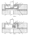
- FIGURE 4 in which the MTJ stack is shown centered over the interconnect metallization 37, is only for exemplary illustration. For example, as seen in FIGURE 5 , the MTJ stack can be off-center.
- the first electrode 30 and/or the reference fixed magnetic layer stack 32 may be subsequently planarized, if needed, to provide a sufficiently flat surface for formation of the tunnel barrier layer 12 and the free layer 11 for control of layer thickness and quality, because these two layers (11 and 12) may be on the order of 1 nm.
- the MTJ structure shown in FIGURE 3 may be referred to as an asymmetrical MTJ.
- the first mask is used to form the stack including the conductive second electrode 6, the free layer 11 and the tunnel barrier layer 12, but not the reference fixed magnetic layer stack 32 or the first electrode 30.
- the reference fixed magnetic layer stack 32 and the first electrode 30 are formed using the second mask.
- the same mask set may be used, however, to form an alternative MTJ structure described as "symmetrical.”
- a "symmetric" structure may be achieved by extending the etch process to include the reference fixed magnetic layer stack 32, but not the first electrode 30.
- the first electrode 30 is patterned using the second mask, as before, i.e., in the "asymmetric" configuration.
- the first electrode 30 and the third electrode 15 only are identically patterned to symmetrically sandwich the intervening magnetic tunnel junction elements 32, 12, and 11 and the second electrode 6 between the first electrode 30 and the third electrode 15.
- the reference fixed magnetic layer stack 32 has the same dimensions (apart from thickness) as the tunnel barrier layer 12, the free layer 11 and the conductive electrode 6.
- a first advantage is the elimination of one critical dimension mask.
- a second advantage is that the critical layers of the MTJ stack (i.e., the conductive second electrode 6, the free layer 11, the fixed layer 12 and, optionally, reference fixed magnetic layer stack 32) are self-aligned by being formed in a single mask step.
- a third advantage is the MTJ stack can be placed right over the metallization interconnect 37. This allows a tighter device pitch density.
- a fourth advantage is that the processes are both fewer in number relative to prior art MTJ formation, lowering process costs, and arc compatible with integrated circuit BEOL processing. In other words, the processes are "integration friendly.”
- An additional advantage is the formation of a design structure for integrating STT MRAM fabrication processes in a BEOL semiconductor integrated circuit design system that may operate on a computer workstation by executing design operations according to operating system software, support files, and design software such as CADENCE or ORCA D.
- MRAM as set forth in the disclosure may operate with logic circuitry such as microprocessors.
- the MRAM may be integrated into devices that employ the microprocessors.
- the MRAM may be part of a communications device.
- the MRAM may include other types of circuitry without departing from the scope of the disclosure.
Landscapes
- Engineering & Computer Science (AREA)
- Computer Hardware Design (AREA)
- Manufacturing & Machinery (AREA)
- Hall/Mr Elements (AREA)
- Mram Or Spin Memory Techniques (AREA)
- Semiconductor Memories (AREA)
Priority Applications (1)
| Application Number | Priority Date | Filing Date | Title |
|---|---|---|---|
| EP20140172609 EP2800159A1 (en) | 2008-04-18 | 2009-04-15 | A magnetic tunnel junction element |
Applications Claiming Priority (3)
| Application Number | Priority Date | Filing Date | Title |
|---|---|---|---|
| US4616708P | 2008-04-18 | 2008-04-18 | |
| US12/405,461 US8125040B2 (en) | 2008-04-18 | 2009-03-17 | Two mask MTJ integration for STT MRAM |
| PCT/US2009/040612 WO2009129283A1 (en) | 2008-04-18 | 2009-04-15 | Manufacturing method of a magnetic tunnel junction element using two masks |
Related Child Applications (2)
| Application Number | Title | Priority Date | Filing Date |
|---|---|---|---|
| EP20140172609 Division-Into EP2800159A1 (en) | 2008-04-18 | 2009-04-15 | A magnetic tunnel junction element |
| EP20140172609 Division EP2800159A1 (en) | 2008-04-18 | 2009-04-15 | A magnetic tunnel junction element |
Publications (2)
| Publication Number | Publication Date |
|---|---|
| EP2277211A1 EP2277211A1 (en) | 2011-01-26 |
| EP2277211B1 true EP2277211B1 (en) | 2014-10-08 |
Family
ID=40791514
Family Applications (2)
| Application Number | Title | Priority Date | Filing Date |
|---|---|---|---|
| EP09732874.4A Not-in-force EP2277211B1 (en) | 2008-04-18 | 2009-04-15 | Manufacturing method of a magnetic tunnel junction element using two masks |
| EP20140172609 Withdrawn EP2800159A1 (en) | 2008-04-18 | 2009-04-15 | A magnetic tunnel junction element |
Family Applications After (1)
| Application Number | Title | Priority Date | Filing Date |
|---|---|---|---|
| EP20140172609 Withdrawn EP2800159A1 (en) | 2008-04-18 | 2009-04-15 | A magnetic tunnel junction element |
Country Status (7)
| Country | Link |
|---|---|
| US (1) | US8125040B2 (OSRAM) |
| EP (2) | EP2277211B1 (OSRAM) |
| JP (3) | JP2011518440A (OSRAM) |
| KR (1) | KR101200008B1 (OSRAM) |
| CN (1) | CN102007614B (OSRAM) |
| TW (1) | TW201007730A (OSRAM) |
| WO (1) | WO2009129283A1 (OSRAM) |
Cited By (1)
| Publication number | Priority date | Publication date | Assignee | Title |
|---|---|---|---|---|
| US20210351340A1 (en) * | 2020-05-08 | 2021-11-11 | International Business Machines Corporation | Via interconnects for a magnetoresistive random-access memory device |
Families Citing this family (43)
| Publication number | Priority date | Publication date | Assignee | Title |
|---|---|---|---|---|
| US20100157644A1 (en) * | 2008-12-19 | 2010-06-24 | Unity Semiconductor Corporation | Configurable memory interface to provide serial and parallel access to memories |
| WO2010151855A2 (en) * | 2009-06-26 | 2010-12-29 | Cornell University | Iii-v semiconductor structures including aluminum-silicon nitride passivation |
| US8558331B2 (en) * | 2009-12-08 | 2013-10-15 | Qualcomm Incorporated | Magnetic tunnel junction device |
| US8681536B2 (en) * | 2010-01-15 | 2014-03-25 | Qualcomm Incorporated | Magnetic tunnel junction (MTJ) on planarized electrode |
| JP2011238679A (ja) * | 2010-05-07 | 2011-11-24 | Fujitsu Semiconductor Ltd | 磁気記憶装置の製造方法及び磁気記憶装置 |
| US8722543B2 (en) | 2010-07-30 | 2014-05-13 | Headway Technologies, Inc. | Composite hard mask with upper sacrificial dielectric layer for the patterning and etching of nanometer size MRAM devices |
| US8547736B2 (en) * | 2010-08-03 | 2013-10-01 | Qualcomm Incorporated | Generating a non-reversible state at a bitcell having a first magnetic tunnel junction and a second magnetic tunnel junction |
| US8928100B2 (en) * | 2011-06-24 | 2015-01-06 | International Business Machines Corporation | Spin transfer torque cell for magnetic random access memory |
| US8921959B2 (en) * | 2011-07-26 | 2014-12-30 | Taiwan Semiconductor Manufacturing Company, Ltd. | MRAM device and fabrication method thereof |
| US9202562B2 (en) | 2012-04-18 | 2015-12-01 | Advanced Integrated Memory Inc. | Method to reduce read error rate for semiconductor resistive memory |
| US9047964B2 (en) | 2012-08-20 | 2015-06-02 | Qualcomm Incorporated | Multi-level memory cell using multiple magnetic tunnel junctions with varying MGO thickness |
| US8901687B2 (en) | 2012-11-27 | 2014-12-02 | Industrial Technology Research Institute | Magnetic device with a substrate, a sensing block and a repair layer |
| KR20210063472A (ko) | 2013-03-15 | 2021-06-01 | 인텔 코포레이션 | 내장된 자기 터널 접합을 포함하는 로직 칩 |
| US9172033B2 (en) | 2013-07-03 | 2015-10-27 | Taiwan Semiconductor Manufacturing Company, Ltd. | MRAM device and fabrication method thereof |
| US8988835B1 (en) | 2013-10-14 | 2015-03-24 | International Business Machines Corporation | Contact recording tunnel magnetoresistive sensor with layer of refractory metal |
| CN104882538B (zh) * | 2014-02-28 | 2017-09-22 | 中芯国际集成电路制造(上海)有限公司 | 环型磁性随机存取存储器单元结构的制造方法 |
| KR102149195B1 (ko) | 2014-03-04 | 2020-08-28 | 에스케이하이닉스 주식회사 | 전자 장치 및 그 제조 방법 |
| US9269893B2 (en) * | 2014-04-02 | 2016-02-23 | Qualcomm Incorporated | Replacement conductive hard mask for multi-step magnetic tunnel junction (MTJ) etch |
| CN105206741B (zh) * | 2014-06-23 | 2019-02-12 | 中芯国际集成电路制造(上海)有限公司 | 磁性隧道结单元和制备磁性隧道结单元的方法 |
| US10043967B2 (en) * | 2014-08-07 | 2018-08-07 | Qualcomm Incorporated | Self-compensation of stray field of perpendicular magnetic elements |
| US10256395B2 (en) | 2015-06-19 | 2019-04-09 | Intel Corporation | Capped magnetic memory |
| US9905751B2 (en) | 2015-10-20 | 2018-02-27 | Taiwan Semiconductor Manufacturing Company, Ltd. | Magnetic tunnel junction with reduced damage |
| CN106676532B (zh) * | 2015-11-10 | 2019-04-05 | 江苏鲁汶仪器有限公司 | 金属刻蚀装置及方法 |
| US9853210B2 (en) * | 2015-11-17 | 2017-12-26 | International Business Machines Corporation | Reduced process degradation of spin torque magnetoresistive random access memory |
| US9515252B1 (en) * | 2015-12-29 | 2016-12-06 | International Business Machines Corporation | Low degradation MRAM encapsulation process using silicon-rich silicon nitride film |
| US9805795B2 (en) | 2016-01-08 | 2017-10-31 | Samsung Electronics Co., Ltd. | Zero leakage, high noise margin coupled giant spin hall based retention latch |
| US9711713B1 (en) * | 2016-01-15 | 2017-07-18 | Taiwan Semiconductor Manufacturing Company Ltd. | Semiconductor structure, electrode structure and method of forming the same |
| US10522749B2 (en) | 2017-05-15 | 2019-12-31 | Taiwan Semiconductor Manufacturing Company, Ltd. | Combined physical and chemical etch to reduce magnetic tunnel junction (MTJ) sidewall damage |
| US10043851B1 (en) | 2017-08-03 | 2018-08-07 | Headway Technologies, Inc. | Etch selectivity by introducing oxidants to noble gas during physical magnetic tunnel junction (MTJ) etching |
| US10359699B2 (en) | 2017-08-24 | 2019-07-23 | Taiwan Semiconductor Manufacturing Company, Ltd. | Self-adaptive halogen treatment to improve photoresist pattern and magnetoresistive random access memory (MRAM) device uniformity |
| US10585630B2 (en) | 2017-09-11 | 2020-03-10 | Samsung Electronics Co., Ltd. | Selectorless 3D stackable memory |
| US10038138B1 (en) | 2017-10-10 | 2018-07-31 | Headway Technologies, Inc. | High temperature volatilization of sidewall materials from patterned magnetic tunnel junctions |
| US10134981B1 (en) | 2017-10-20 | 2018-11-20 | Headway Technologies, Inc. | Free layer sidewall oxidation and spacer assisted magnetic tunnel junction (MTJ) etch for high performance magnetoresistive random access memory (MRAM) devices |
| US10879077B2 (en) | 2017-10-30 | 2020-12-29 | Taiwan Semiconductor Manufacturing Company Ltd. | Planarization apparatus and planarization method thereof |
| US10325639B2 (en) | 2017-11-20 | 2019-06-18 | Taiwan Semiconductor Manufacturing Company, Ltd. | Initialization process for magnetic random access memory (MRAM) production |
| US10153427B1 (en) | 2017-12-28 | 2018-12-11 | Headway Technologies, Inc. | Magnetic tunnel junction (MTJ) performance by introducing oxidants to methanol with or without noble gas during MTJ etch |
| CN109994476B (zh) * | 2017-12-29 | 2021-03-16 | 上海磁宇信息科技有限公司 | 一种制备磁性随机存储器阵列单元的方法 |
| US10475991B2 (en) | 2018-02-22 | 2019-11-12 | Taiwan Semiconductor Manufacturing Company, Ltd. | Fabrication of large height top metal electrode for sub-60nm magnetoresistive random access memory (MRAM) devices |
| US10790002B2 (en) | 2018-06-21 | 2020-09-29 | Samsung Electronics Co., Ltd. | Giant spin hall-based compact neuromorphic cell optimized for differential read inference |
| US11296277B2 (en) | 2018-10-16 | 2022-04-05 | Samsung Electronics Co., Ltd. | Variable resistance memory device having an anti-oxidation layer and a method of manufacturing the same |
| US10971176B2 (en) | 2019-02-21 | 2021-04-06 | International Business Machines Corporation | Tunnel magnetoresistive sensor with adjacent gap having chromium alloy seed layer and refractory material layer |
| US11569442B2 (en) | 2020-06-17 | 2023-01-31 | International Business Machines Corporation | Dielectric retention and method of forming memory pillar |
| US12464955B2 (en) * | 2021-12-09 | 2025-11-04 | Taiwan Semiconductor Manufacturing Co., Ltd. | Magnetic tunnel junction device and method of forming the same |
Family Cites Families (26)
| Publication number | Priority date | Publication date | Assignee | Title |
|---|---|---|---|---|
| JP5013494B2 (ja) * | 2001-04-06 | 2012-08-29 | ルネサスエレクトロニクス株式会社 | 磁性メモリの製造方法 |
| US6631055B2 (en) * | 2001-06-08 | 2003-10-07 | International Business Machines Corporation | Tunnel valve flux guide structure formed by oxidation of pinned layer |
| US6759263B2 (en) | 2002-08-29 | 2004-07-06 | Chentsau Ying | Method of patterning a layer of magnetic material |
| JP2004128229A (ja) * | 2002-10-02 | 2004-04-22 | Nec Corp | 磁性メモリ及びその製造方法 |
| US7394626B2 (en) * | 2002-11-01 | 2008-07-01 | Nec Corporation | Magnetoresistance device with a diffusion barrier between a conductor and a magnetoresistance element and method of fabricating the same |
| KR100615600B1 (ko) * | 2004-08-09 | 2006-08-25 | 삼성전자주식회사 | 고집적 자기램 소자 및 그 제조방법 |
| US6911156B2 (en) | 2003-04-16 | 2005-06-28 | Freescale Semiconductor, Inc. | Methods for fabricating MRAM device structures |
| US20060138576A1 (en) * | 2003-06-24 | 2006-06-29 | Galdis Michael C | Self-aligned conductive lines for fet-based magnetic random access memory devices and method of forming the same |
| KR100568512B1 (ko) * | 2003-09-29 | 2006-04-07 | 삼성전자주식회사 | 열발생층을 갖는 자기열 램셀들 및 이를 구동시키는 방법들 |
| US20050090111A1 (en) * | 2003-10-24 | 2005-04-28 | Heon Lee | Magnetic tunnel junction device with etch stop layer and dielectric spacer |
| US7259062B2 (en) | 2003-10-24 | 2007-08-21 | Hewlett-Packard Development Company, Lp. | Method of making a magnetic tunnel junction device |
| US20050205952A1 (en) * | 2004-03-19 | 2005-09-22 | Jae-Hyun Park | Magnetic random access memory cells having split sub-digit lines having cladding layers thereon and methods of fabricating the same |
| US7105903B2 (en) * | 2004-11-18 | 2006-09-12 | Freescale Semiconductor, Inc. | Methods and structures for electrical communication with an overlying electrode for a semiconductor element |
| KR100647319B1 (ko) * | 2005-02-05 | 2006-11-23 | 삼성전자주식회사 | 스핀 분극 전류를 이용한 멀티 비트 자기 메모리 소자와그 제조 및 구동 방법 |
| US7285836B2 (en) * | 2005-03-09 | 2007-10-23 | Maglabs, Inc. | Magnetic random access memory with stacked memory cells having oppositely-directed hard-axis biasing |
| JP4677589B2 (ja) | 2005-03-18 | 2011-04-27 | 独立行政法人科学技術振興機構 | 伝送回路一体型マイクロ波発生素子並びにマイクロ波検出方法、マイクロ波検出回路、マイクロ波検出素子及び伝送回路一体型マイクロ波検出素子 |
| JP4659518B2 (ja) * | 2005-05-24 | 2011-03-30 | シャープ株式会社 | 磁気抵抗効果素子及びその製造方法 |
| KR100655438B1 (ko) * | 2005-08-25 | 2006-12-08 | 삼성전자주식회사 | 자기 기억 소자 및 그 형성 방법 |
| US7511990B2 (en) * | 2005-09-30 | 2009-03-31 | Everspin Technologies, Inc. | Magnetic tunnel junction temperature sensors |
| JP4991155B2 (ja) * | 2006-01-19 | 2012-08-01 | 株式会社東芝 | 半導体記憶装置 |
| US7732881B2 (en) * | 2006-11-01 | 2010-06-08 | Avalanche Technology, Inc. | Current-confined effect of magnetic nano-current-channel (NCC) for magnetic random access memory (MRAM) |
| JP4560025B2 (ja) * | 2006-09-29 | 2010-10-13 | 株式会社東芝 | 磁気ランダムアクセスメモリ及びその製造方法 |
| US7852662B2 (en) * | 2007-04-24 | 2010-12-14 | Magic Technologies, Inc. | Spin-torque MRAM: spin-RAM, array |
| US7723128B2 (en) * | 2008-02-18 | 2010-05-25 | Taiwan Semiconductor Manufacturing Company, Ltd. | In-situ formed capping layer in MTJ devices |
| US8057925B2 (en) * | 2008-03-27 | 2011-11-15 | Magic Technologies, Inc. | Low switching current dual spin filter (DSF) element for STT-RAM and a method for making the same |
| US20090251950A1 (en) * | 2008-04-08 | 2009-10-08 | Ulrich Klostermann | Integrated Circuit, Memory Cell Arrangement, Thermal Select Magneto-Resistive Memory Cell, Method of Operating a Thermal Select Magneto-Resistive Memory Cell, and Method of Manufacturing a Thermal Select Magneto-Resistive Memory Cell |
-
2009
- 2009-03-17 US US12/405,461 patent/US8125040B2/en active Active
- 2009-04-15 JP JP2011505157A patent/JP2011518440A/ja not_active Withdrawn
- 2009-04-15 WO PCT/US2009/040612 patent/WO2009129283A1/en not_active Ceased
- 2009-04-15 KR KR1020107025861A patent/KR101200008B1/ko not_active Expired - Fee Related
- 2009-04-15 EP EP09732874.4A patent/EP2277211B1/en not_active Not-in-force
- 2009-04-15 CN CN200980112999.6A patent/CN102007614B/zh not_active Expired - Fee Related
- 2009-04-15 EP EP20140172609 patent/EP2800159A1/en not_active Withdrawn
- 2009-04-17 TW TW098112861A patent/TW201007730A/zh unknown
-
2014
- 2014-04-03 JP JP2014077077A patent/JP2014160839A/ja not_active Withdrawn
-
2015
- 2015-02-18 JP JP2015029705A patent/JP2015144287A/ja active Pending
Cited By (2)
| Publication number | Priority date | Publication date | Assignee | Title |
|---|---|---|---|---|
| US20210351340A1 (en) * | 2020-05-08 | 2021-11-11 | International Business Machines Corporation | Via interconnects for a magnetoresistive random-access memory device |
| US11805704B2 (en) * | 2020-05-08 | 2023-10-31 | International Business Machines Corporation | Via interconnects for a magnetoresistive random-access memory device |
Also Published As
| Publication number | Publication date |
|---|---|
| EP2277211A1 (en) | 2011-01-26 |
| WO2009129283A1 (en) | 2009-10-22 |
| EP2800159A1 (en) | 2014-11-05 |
| JP2014160839A (ja) | 2014-09-04 |
| KR101200008B1 (ko) | 2012-11-12 |
| JP2015144287A (ja) | 2015-08-06 |
| JP2011518440A (ja) | 2011-06-23 |
| US20090261437A1 (en) | 2009-10-22 |
| CN102007614B (zh) | 2014-07-16 |
| CN102007614A (zh) | 2011-04-06 |
| TW201007730A (en) | 2010-02-16 |
| KR20110002864A (ko) | 2011-01-10 |
| US8125040B2 (en) | 2012-02-28 |
Similar Documents
| Publication | Publication Date | Title |
|---|---|---|
| EP2277211B1 (en) | Manufacturing method of a magnetic tunnel junction element using two masks | |
| US9159910B2 (en) | One-mask MTJ integration for STT MRAM | |
| US8564079B2 (en) | STT MRAM magnetic tunnel junction architecture and integration | |
| US11005032B2 (en) | Techniques for MRAM MTJ top electrode to metal layer interface including spacer | |
| WO2012019135A2 (en) | Mram device and integration techniques compatible with logic integration | |
| JP2024532824A (ja) | 高さを低くしたmramスタック | |
| US11961544B2 (en) | Spin-orbit torque (SOT) magnetoresistive random-access memory (MRAM) with low resistivity spin hall effect (SHE) write line | |
| CN118555902A (zh) | 磁存储器及其制备方法 | |
| US12324358B2 (en) | Tall bottom electrode structure in embedded magnetoresistive random-access memory |
Legal Events
| Date | Code | Title | Description |
|---|---|---|---|
| PUAI | Public reference made under article 153(3) epc to a published international application that has entered the european phase |
Free format text: ORIGINAL CODE: 0009012 |
|
| 17P | Request for examination filed |
Effective date: 20101103 |
|
| AK | Designated contracting states |
Kind code of ref document: A1 Designated state(s): AT BE BG CH CY CZ DE DK EE ES FI FR GB GR HR HU IE IS IT LI LT LU LV MC MK MT NL NO PL PT RO SE SI SK TR |
|
| AX | Request for extension of the european patent |
Extension state: AL BA RS |
|
| 17Q | First examination report despatched |
Effective date: 20110627 |
|
| DAX | Request for extension of the european patent (deleted) | ||
| GRAP | Despatch of communication of intention to grant a patent |
Free format text: ORIGINAL CODE: EPIDOSNIGR1 |
|
| INTG | Intention to grant announced |
Effective date: 20140424 |
|
| GRAS | Grant fee paid |
Free format text: ORIGINAL CODE: EPIDOSNIGR3 |
|
| GRAA | (expected) grant |
Free format text: ORIGINAL CODE: 0009210 |
|
| AK | Designated contracting states |
Kind code of ref document: B1 Designated state(s): AT BE BG CH CY CZ DE DK EE ES FI FR GB GR HR HU IE IS IT LI LT LU LV MC MK MT NL NO PL PT RO SE SI SK TR |
|
| REG | Reference to a national code |
Ref country code: GB Ref legal event code: FG4D |
|
| REG | Reference to a national code |
Ref country code: CH Ref legal event code: EP Ref country code: AT Ref legal event code: REF Ref document number: 691036 Country of ref document: AT Kind code of ref document: T Effective date: 20141015 |
|
| REG | Reference to a national code |
Ref country code: IE Ref legal event code: FG4D |
|
| REG | Reference to a national code |
Ref country code: DE Ref legal event code: R096 Ref document number: 602009027072 Country of ref document: DE Effective date: 20141120 |
|
| REG | Reference to a national code |
Ref country code: NL Ref legal event code: VDEP Effective date: 20141008 |
|
| REG | Reference to a national code |
Ref country code: AT Ref legal event code: MK05 Ref document number: 691036 Country of ref document: AT Kind code of ref document: T Effective date: 20141008 |
|
| REG | Reference to a national code |
Ref country code: LT Ref legal event code: MG4D |
|
| PG25 | Lapsed in a contracting state [announced via postgrant information from national office to epo] |
Ref country code: NL Free format text: LAPSE BECAUSE OF FAILURE TO SUBMIT A TRANSLATION OF THE DESCRIPTION OR TO PAY THE FEE WITHIN THE PRESCRIBED TIME-LIMIT Effective date: 20141008 |
|
| PG25 | Lapsed in a contracting state [announced via postgrant information from national office to epo] |
Ref country code: FI Free format text: LAPSE BECAUSE OF FAILURE TO SUBMIT A TRANSLATION OF THE DESCRIPTION OR TO PAY THE FEE WITHIN THE PRESCRIBED TIME-LIMIT Effective date: 20141008 Ref country code: NO Free format text: LAPSE BECAUSE OF FAILURE TO SUBMIT A TRANSLATION OF THE DESCRIPTION OR TO PAY THE FEE WITHIN THE PRESCRIBED TIME-LIMIT Effective date: 20150108 Ref country code: PT Free format text: LAPSE BECAUSE OF FAILURE TO SUBMIT A TRANSLATION OF THE DESCRIPTION OR TO PAY THE FEE WITHIN THE PRESCRIBED TIME-LIMIT Effective date: 20150209 Ref country code: LT Free format text: LAPSE BECAUSE OF FAILURE TO SUBMIT A TRANSLATION OF THE DESCRIPTION OR TO PAY THE FEE WITHIN THE PRESCRIBED TIME-LIMIT Effective date: 20141008 Ref country code: ES Free format text: LAPSE BECAUSE OF FAILURE TO SUBMIT A TRANSLATION OF THE DESCRIPTION OR TO PAY THE FEE WITHIN THE PRESCRIBED TIME-LIMIT Effective date: 20141008 Ref country code: IS Free format text: LAPSE BECAUSE OF FAILURE TO SUBMIT A TRANSLATION OF THE DESCRIPTION OR TO PAY THE FEE WITHIN THE PRESCRIBED TIME-LIMIT Effective date: 20150208 |
|
| PG25 | Lapsed in a contracting state [announced via postgrant information from national office to epo] |
Ref country code: AT Free format text: LAPSE BECAUSE OF FAILURE TO SUBMIT A TRANSLATION OF THE DESCRIPTION OR TO PAY THE FEE WITHIN THE PRESCRIBED TIME-LIMIT Effective date: 20141008 Ref country code: GR Free format text: LAPSE BECAUSE OF FAILURE TO SUBMIT A TRANSLATION OF THE DESCRIPTION OR TO PAY THE FEE WITHIN THE PRESCRIBED TIME-LIMIT Effective date: 20150109 Ref country code: PL Free format text: LAPSE BECAUSE OF FAILURE TO SUBMIT A TRANSLATION OF THE DESCRIPTION OR TO PAY THE FEE WITHIN THE PRESCRIBED TIME-LIMIT Effective date: 20141008 Ref country code: CY Free format text: LAPSE BECAUSE OF FAILURE TO SUBMIT A TRANSLATION OF THE DESCRIPTION OR TO PAY THE FEE WITHIN THE PRESCRIBED TIME-LIMIT Effective date: 20141008 Ref country code: SE Free format text: LAPSE BECAUSE OF FAILURE TO SUBMIT A TRANSLATION OF THE DESCRIPTION OR TO PAY THE FEE WITHIN THE PRESCRIBED TIME-LIMIT Effective date: 20141008 Ref country code: HR Free format text: LAPSE BECAUSE OF FAILURE TO SUBMIT A TRANSLATION OF THE DESCRIPTION OR TO PAY THE FEE WITHIN THE PRESCRIBED TIME-LIMIT Effective date: 20141008 Ref country code: LV Free format text: LAPSE BECAUSE OF FAILURE TO SUBMIT A TRANSLATION OF THE DESCRIPTION OR TO PAY THE FEE WITHIN THE PRESCRIBED TIME-LIMIT Effective date: 20141008 |
|
| REG | Reference to a national code |
Ref country code: DE Ref legal event code: R097 Ref document number: 602009027072 Country of ref document: DE |
|
| PG25 | Lapsed in a contracting state [announced via postgrant information from national office to epo] |
Ref country code: EE Free format text: LAPSE BECAUSE OF FAILURE TO SUBMIT A TRANSLATION OF THE DESCRIPTION OR TO PAY THE FEE WITHIN THE PRESCRIBED TIME-LIMIT Effective date: 20141008 Ref country code: CZ Free format text: LAPSE BECAUSE OF FAILURE TO SUBMIT A TRANSLATION OF THE DESCRIPTION OR TO PAY THE FEE WITHIN THE PRESCRIBED TIME-LIMIT Effective date: 20141008 Ref country code: RO Free format text: LAPSE BECAUSE OF FAILURE TO SUBMIT A TRANSLATION OF THE DESCRIPTION OR TO PAY THE FEE WITHIN THE PRESCRIBED TIME-LIMIT Effective date: 20141008 Ref country code: DK Free format text: LAPSE BECAUSE OF FAILURE TO SUBMIT A TRANSLATION OF THE DESCRIPTION OR TO PAY THE FEE WITHIN THE PRESCRIBED TIME-LIMIT Effective date: 20141008 Ref country code: SK Free format text: LAPSE BECAUSE OF FAILURE TO SUBMIT A TRANSLATION OF THE DESCRIPTION OR TO PAY THE FEE WITHIN THE PRESCRIBED TIME-LIMIT Effective date: 20141008 |
|
| PLBE | No opposition filed within time limit |
Free format text: ORIGINAL CODE: 0009261 |
|
| STAA | Information on the status of an ep patent application or granted ep patent |
Free format text: STATUS: NO OPPOSITION FILED WITHIN TIME LIMIT |
|
| PG25 | Lapsed in a contracting state [announced via postgrant information from national office to epo] |
Ref country code: IT Free format text: LAPSE BECAUSE OF FAILURE TO SUBMIT A TRANSLATION OF THE DESCRIPTION OR TO PAY THE FEE WITHIN THE PRESCRIBED TIME-LIMIT Effective date: 20141008 |
|
| 26N | No opposition filed |
Effective date: 20150709 |
|
| PG25 | Lapsed in a contracting state [announced via postgrant information from national office to epo] |
Ref country code: LU Free format text: LAPSE BECAUSE OF FAILURE TO SUBMIT A TRANSLATION OF THE DESCRIPTION OR TO PAY THE FEE WITHIN THE PRESCRIBED TIME-LIMIT Effective date: 20150415 Ref country code: MC Free format text: LAPSE BECAUSE OF FAILURE TO SUBMIT A TRANSLATION OF THE DESCRIPTION OR TO PAY THE FEE WITHIN THE PRESCRIBED TIME-LIMIT Effective date: 20141008 |
|
| REG | Reference to a national code |
Ref country code: CH Ref legal event code: PL |
|
| REG | Reference to a national code |
Ref country code: IE Ref legal event code: MM4A |
|
| PG25 | Lapsed in a contracting state [announced via postgrant information from national office to epo] |
Ref country code: LI Free format text: LAPSE BECAUSE OF NON-PAYMENT OF DUE FEES Effective date: 20150430 Ref country code: CH Free format text: LAPSE BECAUSE OF NON-PAYMENT OF DUE FEES Effective date: 20150430 |
|
| REG | Reference to a national code |
Ref country code: FR Ref legal event code: ST Effective date: 20151231 |
|
| PG25 | Lapsed in a contracting state [announced via postgrant information from national office to epo] |
Ref country code: SI Free format text: LAPSE BECAUSE OF FAILURE TO SUBMIT A TRANSLATION OF THE DESCRIPTION OR TO PAY THE FEE WITHIN THE PRESCRIBED TIME-LIMIT Effective date: 20141008 Ref country code: FR Free format text: LAPSE BECAUSE OF NON-PAYMENT OF DUE FEES Effective date: 20150430 |
|
| PG25 | Lapsed in a contracting state [announced via postgrant information from national office to epo] |
Ref country code: IE Free format text: LAPSE BECAUSE OF NON-PAYMENT OF DUE FEES Effective date: 20150415 |
|
| PG25 | Lapsed in a contracting state [announced via postgrant information from national office to epo] |
Ref country code: MT Free format text: LAPSE BECAUSE OF FAILURE TO SUBMIT A TRANSLATION OF THE DESCRIPTION OR TO PAY THE FEE WITHIN THE PRESCRIBED TIME-LIMIT Effective date: 20141008 |
|
| PG25 | Lapsed in a contracting state [announced via postgrant information from national office to epo] |
Ref country code: HU Free format text: LAPSE BECAUSE OF FAILURE TO SUBMIT A TRANSLATION OF THE DESCRIPTION OR TO PAY THE FEE WITHIN THE PRESCRIBED TIME-LIMIT; INVALID AB INITIO Effective date: 20090415 Ref country code: BG Free format text: LAPSE BECAUSE OF FAILURE TO SUBMIT A TRANSLATION OF THE DESCRIPTION OR TO PAY THE FEE WITHIN THE PRESCRIBED TIME-LIMIT Effective date: 20141008 |
|
| PG25 | Lapsed in a contracting state [announced via postgrant information from national office to epo] |
Ref country code: TR Free format text: LAPSE BECAUSE OF FAILURE TO SUBMIT A TRANSLATION OF THE DESCRIPTION OR TO PAY THE FEE WITHIN THE PRESCRIBED TIME-LIMIT Effective date: 20141008 |
|
| PG25 | Lapsed in a contracting state [announced via postgrant information from national office to epo] |
Ref country code: BE Free format text: LAPSE BECAUSE OF FAILURE TO SUBMIT A TRANSLATION OF THE DESCRIPTION OR TO PAY THE FEE WITHIN THE PRESCRIBED TIME-LIMIT Effective date: 20141008 |
|
| PGFP | Annual fee paid to national office [announced via postgrant information from national office to epo] |
Ref country code: GB Payment date: 20180328 Year of fee payment: 10 |
|
| PG25 | Lapsed in a contracting state [announced via postgrant information from national office to epo] |
Ref country code: MK Free format text: LAPSE BECAUSE OF FAILURE TO SUBMIT A TRANSLATION OF THE DESCRIPTION OR TO PAY THE FEE WITHIN THE PRESCRIBED TIME-LIMIT Effective date: 20141008 |
|
| GBPC | Gb: european patent ceased through non-payment of renewal fee |
Effective date: 20190415 |
|
| PG25 | Lapsed in a contracting state [announced via postgrant information from national office to epo] |
Ref country code: GB Free format text: LAPSE BECAUSE OF NON-PAYMENT OF DUE FEES Effective date: 20190415 |
|
| PGFP | Annual fee paid to national office [announced via postgrant information from national office to epo] |
Ref country code: DE Payment date: 20200317 Year of fee payment: 12 |
|
| REG | Reference to a national code |
Ref country code: DE Ref legal event code: R119 Ref document number: 602009027072 Country of ref document: DE |
|
| PG25 | Lapsed in a contracting state [announced via postgrant information from national office to epo] |
Ref country code: DE Free format text: LAPSE BECAUSE OF NON-PAYMENT OF DUE FEES Effective date: 20211103 |