EP2273483B1 - Anzeigevorrichtung mit aktiver Matrix und Steuerverfahren dafür - Google Patents
Anzeigevorrichtung mit aktiver Matrix und Steuerverfahren dafür Download PDFInfo
- Publication number
- EP2273483B1 EP2273483B1 EP10012956.8A EP10012956A EP2273483B1 EP 2273483 B1 EP2273483 B1 EP 2273483B1 EP 10012956 A EP10012956 A EP 10012956A EP 2273483 B1 EP2273483 B1 EP 2273483B1
- Authority
- EP
- European Patent Office
- Prior art keywords
- cycle
- video signal
- signal
- vertical synchronizing
- driving circuit
- Prior art date
- Legal status (The legal status is an assumption and is not a legal conclusion. Google has not performed a legal analysis and makes no representation as to the accuracy of the status listed.)
- Expired - Lifetime
Links
- 238000000034 method Methods 0.000 title claims description 39
- 239000011159 matrix material Substances 0.000 title claims description 19
- 230000004044 response Effects 0.000 claims description 82
- 239000004973 liquid crystal related substance Substances 0.000 claims description 45
- 230000001419 dependent effect Effects 0.000 claims description 10
- 238000006243 chemical reaction Methods 0.000 claims description 4
- 230000001902 propagating effect Effects 0.000 claims 2
- 238000010586 diagram Methods 0.000 description 21
- 230000008859 change Effects 0.000 description 19
- 239000000758 substrate Substances 0.000 description 18
- 239000000463 material Substances 0.000 description 15
- 230000014509 gene expression Effects 0.000 description 14
- 230000003247 decreasing effect Effects 0.000 description 5
- 230000005540 biological transmission Effects 0.000 description 4
- 239000011521 glass Substances 0.000 description 4
- 239000004988 Nematic liquid crystal Substances 0.000 description 3
- 238000011156 evaluation Methods 0.000 description 3
- 230000000644 propagated effect Effects 0.000 description 3
- 230000009467 reduction Effects 0.000 description 3
- 230000000694 effects Effects 0.000 description 2
- 230000005684 electric field Effects 0.000 description 2
- 239000010408 film Substances 0.000 description 2
- 208000028485 lattice corneal dystrophy type I Diseases 0.000 description 2
- ORQBXQOJMQIAOY-UHFFFAOYSA-N nobelium Chemical compound [No] ORQBXQOJMQIAOY-UHFFFAOYSA-N 0.000 description 2
- 230000000007 visual effect Effects 0.000 description 2
- -1 TFT Chemical compound 0.000 description 1
- 238000007796 conventional method Methods 0.000 description 1
- 239000013078 crystal Substances 0.000 description 1
- 230000007423 decrease Effects 0.000 description 1
- 230000001747 exhibiting effect Effects 0.000 description 1
- 230000006870 function Effects 0.000 description 1
- 238000012986 modification Methods 0.000 description 1
- 230000004048 modification Effects 0.000 description 1
- 230000000630 rising effect Effects 0.000 description 1
- 238000012360 testing method Methods 0.000 description 1
- 239000010409 thin film Substances 0.000 description 1
Images


Classifications
-
- G—PHYSICS
- G09—EDUCATION; CRYPTOGRAPHY; DISPLAY; ADVERTISING; SEALS
- G09G—ARRANGEMENTS OR CIRCUITS FOR CONTROL OF INDICATING DEVICES USING STATIC MEANS TO PRESENT VARIABLE INFORMATION
- G09G3/00—Control arrangements or circuits, of interest only in connection with visual indicators other than cathode-ray tubes
- G09G3/20—Control arrangements or circuits, of interest only in connection with visual indicators other than cathode-ray tubes for presentation of an assembly of a number of characters, e.g. a page, by composing the assembly by combination of individual elements arranged in a matrix no fixed position being assigned to or needed to be assigned to the individual characters or partial characters
- G09G3/34—Control arrangements or circuits, of interest only in connection with visual indicators other than cathode-ray tubes for presentation of an assembly of a number of characters, e.g. a page, by composing the assembly by combination of individual elements arranged in a matrix no fixed position being assigned to or needed to be assigned to the individual characters or partial characters by control of light from an independent source
- G09G3/36—Control arrangements or circuits, of interest only in connection with visual indicators other than cathode-ray tubes for presentation of an assembly of a number of characters, e.g. a page, by composing the assembly by combination of individual elements arranged in a matrix no fixed position being assigned to or needed to be assigned to the individual characters or partial characters by control of light from an independent source using liquid crystals
- G09G3/3611—Control of matrices with row and column drivers
- G09G3/3648—Control of matrices with row and column drivers using an active matrix
-
- G—PHYSICS
- G09—EDUCATION; CRYPTOGRAPHY; DISPLAY; ADVERTISING; SEALS
- G09G—ARRANGEMENTS OR CIRCUITS FOR CONTROL OF INDICATING DEVICES USING STATIC MEANS TO PRESENT VARIABLE INFORMATION
- G09G3/00—Control arrangements or circuits, of interest only in connection with visual indicators other than cathode-ray tubes
- G09G3/20—Control arrangements or circuits, of interest only in connection with visual indicators other than cathode-ray tubes for presentation of an assembly of a number of characters, e.g. a page, by composing the assembly by combination of individual elements arranged in a matrix no fixed position being assigned to or needed to be assigned to the individual characters or partial characters
- G09G3/34—Control arrangements or circuits, of interest only in connection with visual indicators other than cathode-ray tubes for presentation of an assembly of a number of characters, e.g. a page, by composing the assembly by combination of individual elements arranged in a matrix no fixed position being assigned to or needed to be assigned to the individual characters or partial characters by control of light from an independent source
- G09G3/36—Control arrangements or circuits, of interest only in connection with visual indicators other than cathode-ray tubes for presentation of an assembly of a number of characters, e.g. a page, by composing the assembly by combination of individual elements arranged in a matrix no fixed position being assigned to or needed to be assigned to the individual characters or partial characters by control of light from an independent source using liquid crystals
- G09G3/3611—Control of matrices with row and column drivers
-
- G—PHYSICS
- G09—EDUCATION; CRYPTOGRAPHY; DISPLAY; ADVERTISING; SEALS
- G09G—ARRANGEMENTS OR CIRCUITS FOR CONTROL OF INDICATING DEVICES USING STATIC MEANS TO PRESENT VARIABLE INFORMATION
- G09G2320/00—Control of display operating conditions
- G09G2320/02—Improving the quality of display appearance
- G09G2320/0261—Improving the quality of display appearance in the context of movement of objects on the screen or movement of the observer relative to the screen
-
- G—PHYSICS
- G09—EDUCATION; CRYPTOGRAPHY; DISPLAY; ADVERTISING; SEALS
- G09G—ARRANGEMENTS OR CIRCUITS FOR CONTROL OF INDICATING DEVICES USING STATIC MEANS TO PRESENT VARIABLE INFORMATION
- G09G2320/00—Control of display operating conditions
- G09G2320/10—Special adaptations of display systems for operation with variable images
-
- G—PHYSICS
- G09—EDUCATION; CRYPTOGRAPHY; DISPLAY; ADVERTISING; SEALS
- G09G—ARRANGEMENTS OR CIRCUITS FOR CONTROL OF INDICATING DEVICES USING STATIC MEANS TO PRESENT VARIABLE INFORMATION
- G09G2340/00—Aspects of display data processing
- G09G2340/04—Changes in size, position or resolution of an image
- G09G2340/0407—Resolution change, inclusive of the use of different resolutions for different screen areas
- G09G2340/0435—Change or adaptation of the frame rate of the video stream
-
- G—PHYSICS
- G09—EDUCATION; CRYPTOGRAPHY; DISPLAY; ADVERTISING; SEALS
- G09G—ARRANGEMENTS OR CIRCUITS FOR CONTROL OF INDICATING DEVICES USING STATIC MEANS TO PRESENT VARIABLE INFORMATION
- G09G2360/00—Aspects of the architecture of display systems
- G09G2360/18—Use of a frame buffer in a display terminal, inclusive of the display panel
Definitions
- the present invention relates to a display device and a method for driving the same. More particularly, the present invention relates to a display device including a thin film transistor (hereinafter referred to as TFT) as a switching element for each pixel, such as an active matrix liquid crystal display device, and a method for driving the same.
- TFT thin film transistor
- Prior art document EP 0 487 140 A1 discloses an active matrix liquid crystal video display system comprising a display panel having a row and column matrix array of liquid crystal picture elements with respective controlling switching devices for displaying video information such as TV pictures, and a drive circuit for driving the picture elements to which a video, e.g. TV, signal of given field frequency is supplied.
- a video e.g. TV
- the display panel is driven at a field rate higher than that of the supplied video signal.
- the drive circuit includes a field rate conversion circuit comprising field stores.
- LCD liquid crystal display
- an active matrix LCD device has an excellent display image without crosstalk between adjacent pixels even when the number of pixels is increased. For this reason, the active matrix LCD device has been widely used as a display for digital systems such as a computer.
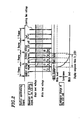
- Such an active matrix LCD device includes an LCD panel 10 and a driving circuit 356, for example, as shown in Figure 11 .
- the LCD panel 10 includes a pair of electrode substrates having a liquid crystal material therebetween.
- a polarizer is attached on the outer surface of each electrode substrate.
- One of the electrode substrates is a TFT array substrate.
- the other electrode substrate is a counter substrate.
- the TFT array substrate is made of a transparent, insulative substrate such as glass.
- a plurality of signal lines S(1), S(2), ⁇ , S(1), ⁇ , S(N), and a plurality of scanning lines G(1), G( 2 ), ⁇ , G(j), ⁇ , G(M) are provided in a matrix.
- a switching element 102, such as TFT, is provided at each intersection of a signal line 201 and a scanning line 301.
- the switching element 102 is connected to a pixel electrode 103.
- An alignment film is provided on substantially an entire surface of the TFT array substrate, covering those lines and elements.
- the counter substrate is made of a transparent, insulative substrate such as glass, as is the TFT array substrate.
- a counter electrode 105 and an alignment film are successively provided on an entire surface of the counter substrate.
- a display cell (pixel) 1 is a portion of a liquid crystal layer sandwiched between the pixel electrode 103 and the counter electrode 105. A matrix of such pixels is provided in the LCD panel 10 .
- the driving circuit 356 includes a write circuit 250 and a timing control circuit 400.
- the write circuit 250 includes a scanning line driving circuit 300 connected to the scanning lines 301, a signal line driving circuit 200 connected to the signal lines 201, and a counter electrode driving circuit (not shown) connected to the counter electrodes 105.
- the timing control circuit 400 is connected to the signal line driving circuit 200 and the scanning line driving circuit 300.
- the scanning line driving circuit (gate driver) 300 includes a shift register and a select switch.
- the shift register includes M flip-flops in cascade connection.
- the select switch is switched in response to an output from each flip-flop.
- a gate scanning voltage Vgh which is sufficient to switch the TFT 102 to the ON state, or a gate holding voltage Vgl, which is sufficient to switch the TFT 102 to the OFF state, is input to the scanning line driving circuit 300.
- the voltage Vgh or Vgl is successively propagated through the flip-flops while being output from the respective select switches.
- the select switch outputs the voltage Vgh to the scanning line 301 in a scanning period of time (TH) to switch the TFT 102 to the ON state.
- the select switch outputs the voltage Vgl to the scanning line 301 to switch the TFT 102 to the OFF state. Timing of the output is controlled by the timing control circuit 400.
- Such an operation writes into a display cell (pixel) 1 a video signal output onto the TFT via the signal line 201 from the signal line driving circuit 200.
- the video signal is written into the pixel 1 via the TFT 102 in the scanning period of time (which is typically equal to a horizontal synchronization period, e.g., several tens of micro seconds). Thereafter, the voltage is held in the pixel 1 until a next write operation starts, i.e., a vertical synchronization period (a frame period). This allows the video signal to be displayed on the display device.
- a horizontal synchronization period e.g., several tens of micro seconds
- LCD devices have been commonly used for displaying not only still pictures but also moving pictures, owing to high-performance computers, etc. Further, large-size liquid crystal televisions have come into practice. Accordingly, high-quality display performance is required for the LCD devices.
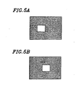
- a white quadrangle is displayed in the black background; and the quadrangle is moved from the left to the right.
- the contour of the moving quadrangle is blurred as shown in Figure 12 B.
- Picture quality may be evaluated on the following two scales: (1) a transit response time which is a period of time during which a display changes from white to black or from black to white, i.e., a change in luminance from 10% to 90% or 90% to 10%; and (2) a human perceptive response time which is a period of time during which a human perceives a change in a luminance level from 0% to 100% or 100% to 0%.
- a transit response time which is a period of time during which a display changes from white to black or from black to white, i.e., a change in luminance from 10% to 90% or 90% to 10%
- a human perceptive response time which is a period of time during which a human perceives a change in a luminance level from 0% to 100% or 100% to 0%.
- a response time which it takes for a human to perceive a change in a luminance level from 0% to 100% or 100% to 0% is defined as Td_LCD (black display to white display) or Tr_LCD (white display to black display), respectively.
- Tr_LCD black display to white display
- Tr_LCD white display to black display
- the response time of a display device which is required for non-blurred moving picture display is not strictly defined, since it significantly varies depending on the size of a moving picture and the background or among individuals.
- a moving picture response limit time Tmov is assumed to about 20 ms.
- the moving picture response limit time Tmov is applied to the case of the luminance change from black display to white display as well as the case of the luminance change from white display to black display.
- Tr_LC which is a period of time which it takes a liquid crystal molecule to change the orientation toward the vertical direction due to an applied electric field
- Td_LC which is a period of time which it takes a liquid crystal molecule to return to the original state due to an intermolecular force in the absence of an applied electric field.
- Tr_LC is substantially equal to Td_LC and Tr_LC and Td_LC can be achieved to be as small as 5 ms.
- This response speed is sufficiently fast as compared with the above-described moving picture response limit time Tmov (-20 ms).
- Tmov moving picture response limit time
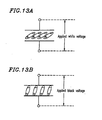
- Figures 13A and 13B are diagrams illustrating a liquid crystal display cell.
- Figure 13A shows a white display state of the cell in the presence of an applied voltage having a white level.
- Figure 13B shows a black display state of the cell in the presence of an applied voltage having a black level.
- the liquid crystal display cell of the LCD device displays a video signal when a voltage is applied across the cell so that the alignment of liquid crystal molecules therein is changed.
- the liquid crystal molecule has a dielectric anisotropy property (the dielectric constant ⁇ s in the major axis direction is different from the dielectric constant ⁇ p in the minor axis direction). For this reason, the capacitance of the LCD cell varies depending on an applied voltage.
- Clc white ⁇ ⁇ 0 ⁇ ⁇ sw / d ⁇ S
- Clc black ⁇ ⁇ 0 ⁇ ⁇ pb / d ⁇ S
- esw is the relative dielectric constant upon the white display, i.e., in the presence of a white level voltage
- ⁇ pb is the relative dielectric constant upon the black display, i.e., in the presence of a black level voltage
- ⁇ 0 is the vacuum dielectric constant
- S is the electrode area of the LCD cell
- d is the distance between the electrodes (cell gap).
- Figure 14 shows a voltage-dependent capacitance characteristic of the LCD cell where the capacitance of the LCD cell upon the white display, i.e., in the presence of a white level voltage is defined as 1. Since esw ⁇ epb is established, the capacitance of the LCD cell upon the black display is larger than the capacitance of the LCD cell upon the white display, as shown in Figure 14 . The ratio is about two to one, depending on what material is used.
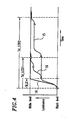
- FIG 15 is a diagram showing the relationship between a voltage change and a display response time (Tr_LCD2) with respect to an arbitrary LCD cell of an LCD device when the white display is switched to the black display.
- the liquid crystal is typically driven by an alternating current from a reliability point of view. Accordingly, a holding voltage of the LCD cell should be driven in such a way to change the polarity of the holding voltage in the frame-by-frame basis.
- a waveform obtained by driving the liquid crystal by a direct current is herein illustrated.
- a synchronizing signal is supplied to the display device along with a video signal.
- a vertical synchronizing signal which determines one frame cycle is included in the synchronizing signal.
- a scanning line voltage is a scanning signal output onto the scanning line G(j) from the scanning driving circuit 300 ( Figure 11 ).
- a signal line applied voltage is a video signal output onto the signal line S(i) from the signal line driving circuit 200.
- the LCD cell holding voltage is shown by a voltage waveform of one LCD cell provided at the intersection of the scanning line G(j) and the signal line S(i).
- a white level voltage is applied across the LCD cell so that the white display state is held.
- the capacitance of the LCD cell is Clc(white).
- the TFT is switched to the ON state by the scanning line voltage, and the black level voltage applied on the scanning line is supplied to the LCD cell to peform a first write operation.
- the time period T3 is equal to one horizontal synchronization period, i.e., tens of micro seconds.
- the liquid crystal material itself has a response time of about 5 ms. The liquid crystal material does not respond during the time period T3 (tens of micro seconds).
- the black level voltage is applied across the LCD cell, the capacitance of the LCD cell remains Clc(white).
- the electric charge of the LCD cell is Qlc-(black level voltage) ⁇ Clc(white).
- T4 the TFT is switched to the OFF state.
- the LCD cell is separated from the signal line, establishing the law of conservation of electric charge.
- the alignment of the liquid crystal is gradually changed in accordance with the holding voltage applied across the liquid crystal. This leads to an increase in the capacitance of the LCD cell.
- the TFT is in the OFF state and therefore the electric charge of the LCD cell is conserved, so that the voltage of the LCD cell is decreased.
- the voltage of the LCD cell is decreased during the time period T4, so that the LCD cell reaches only an intermediate luminance.
- the black level voltage is applied across the LCD cell again, and a second write operation is performed.
- the capacitance of the LCD cell is not switched to Clc(black), similar to the first write operation. For this reason, the voltage is decreased during a holding period of time T6.
- the above-described write operation is repeated until the LCD cell reaches the black level.
- the black display is obtained by a third write operation in which the black level voltage is supplied again during a time period T7.
- a write operation cycle of the LCD cell is equal to a frame cycle determined by the vertical synchronizing signal. Therefore, even when the black level voltage is supplied to the LCD cell in the white display state, the black display state is not obtained in the one frame cycle.
- three frame cycles are required to obtain the black display.
- a frame frequency is typically about 60 Hz (a frame cycle is equal to about 17 ms).
- Japanese Patent Application JP 60257497 A a method for driving an LCD device in which a video signal is stored in a memory; the video signal is alternately supplied to a liquid crystal panel which is divided into upper and lower portions; and thus the write operation cycle is shortened.
- This prior technique is for the purpose of reducing a flicker of the LCD panel.
- applicant's attention has been captured by a change in capacitance of an LCD cell when a black display is switched to a white display or vice versa, which is a property specific to the active matrix driving LCD device. A display in response to a fast moving picture is improved using such a property.
- an object of the present invention is different from that of the prior technique.
- the panel is divided into the upper and lower portions.
- the upper and lower portions of the panel are alternately driven in the following way. A first scanning line of the upper portion is driven; a first scanning line of the lower portion is then driven; a second scanning line of the upper portion is then driven; a second scanning of the lower portion is then driven; etc. In this way, the cycle of the write operation is shortened.
- Such a complicated driving method is not adopted in this invention.
- Japanese Laid-Open Publication No. 9-265073 discloses a method for driving a nematic liquid crystal in which a voltage is repeatedly applied a number of times across a nematic liquid crystal element such as super twisted nematic (STN) in order to improve the response speed of the nematic liquid crystal.
- STN super twisted nematic
- Such a prior technique leads to a reduction in cycle of the applied voltage, which is the same feature of the present invention.
- a number of ON operations are integrated.
- the ON operation is superior to an OFF operation in terms of an operational response, because of the relationship of ON-OFF operations (integral/differential operations), i.e., a time constant waveform has a rapidly rising edge and a slowly falling edge.
- an intended voltage is not obtained by a first write operation.
- the intended voltage is obtained in every write operation, there is a problem in that the voltage is decreased in a subsequent holding period of time.
- the present invention is provided to solve such a problem.
- T. Kurita "Display System for Hold Type Display and Image Quality of Moving Pictures” (Japanese Liquid Crystal Society First LCD Forum, Aug. 28, 1998 ), discloses a method for scanning a device using a field frequency two times or more as high as a standard frequency in which image quality of moving pictures can be improved.
- the present invention and the prior technique have the same feature in that a cycle of write operation is shortened.
- the prior technique describes that blur is prevented because pixels in a narrow spatial range are integrated by the visual system similar to the shutter effect.
- our attention has been captured by a change in capacitance of an LCD cell during a holding period of time after the writing of a voltage into the LCD cell, which is a phenomenon specific to the active matrix driving LCD device. Accordingly, the present invention is a technique different from the prior technique.
- an input video signal is written into each LCD cell with a cycle shorter than the cycle of a vertical synchronizing signal. Therefore, the response speed of the LCD cell can be accelerated regardless of the frame frequency of the external input video signal, thereby obtaining satisfactory moving picture display or the like. Further, the input signal may have the same signal cycle as that of the conventional devices, thereby obtaining device compatibility.
- cycle of a vertical synchronizing signal roughly means a cycle in which a screen of a video signal is switched to another screen.
- a non-interlaced signal such as a computer signal
- frame cycle In the case of a non-interlaced signal such as a computer signal, it is equal to a "frame cycle”.
- an interlaced signal such as a television signal (e.g., a NTSC signal)
- a black level voltage is written one time via a switching element such as a TFT into a pixel such as an LCD cell which has a voltage-dependent capacitance characteristic.
- the voltage of the LCD cell decreases during a holding time due to a change in the capacitance of the LCD cell. For this reason, a plurality of write operations are required to hold an intended voltage, resulting in elongation of the response time to obtain the black display.
- a cycle of the write operation is accelerated in such a way as to satisfy TW1 ⁇ NsTmov
- TW1 is the write operation cycle for each pixel
- N is the number of write operations required to hold the intended voltage during the holding time after the video signal is written
- Tmov is the response limit time required to display a moving image without blur.
- a write operation may be switched between the following two ways in accordance with the frequency of a vertical synchronizing signal (frame frequency or field frequency): (1) the video signal is written into each pixel with a cycle shorter than one cycle of the vertical synchronizing signal (frame cycle or field cycle); and (2) the video signal is written into each pixel with the same cycle as one cycle of the vertical synchronizing signal (frame cycle or field cycle). Therefore, when suspending the operation that the video signal is written into each pixel with a cycle shorter than one cycle of the vertical synchronizing signal (frame cycle or field cycle), power consumption can be lowered.
- the write operation may be switched between the following two ways in accordance with the input mode control signal: (1) the video signal is written into each pixel with a cycle shorter than one cycle of the vertical synchronizing signal (frame cycle or field cycle); and (2) the video signal is written into each pixel with the same cycle as one cycle of the vertical synchronizing signal (frame cycle or field cycle).
- the video signal is written into each pixel with a cycle shorter than one cycle of the vertical synchronizing signal (frame cycle or field cycle).
- the video signal is written into each pixel with the same cycle as one cycle of the vertical synchronizing signal (frame cycle or field cycle).
- operations of circuits having large power consumption such as a frame memory and a control circuit thereof, are suspended, so that power consumption can be further lowered.
- the video signal is written into each pixel with a cycle shorter than one cycle of the vertical synchronizing signal (frame cycle or field cycle).
- the video signal may be written into each pixel with a cycle 1/X times one cycle of the vertical synchronizing signal (frame cycle or field cycle) where X is an arbitrary constant more than one.
- the video signal may be written into each pixel with a cycle 1/Y times one cycle of the vertical synchronizing signal (frame cycle or field cycle) where Y is an arbitrary variable parameter more than one.
- the write operation of the video signal can be performed with a sufficiently short cycle in accordance with a video signal having various frame cycles.
- the video signal may be written into each pixel with a specific cycle Z regardless of the cycle of the vertical synchronizing signal (frame cycle or field cycle).
- the display device can be driven with a specific optimal written operation cycle even when the input video signal has various frame cycles.
- the invention described herein makes possible the advantages of providing a display device and a method for driving the display device, which can provide moving picture display having a high quality. This is achieved by preventing a reduction in a response speed which is caused by a voltage-dependent capacitance change of a display cell such as liquid crystal.
- an LCD cell has a voltage-dependent capacitance characteristic. For this reason, one write operation of the black level voltage into the LCD cell in the white display state via the TFT does not accomplish an intended voltage. A plurality of write operations are required to hold the intended voltage so as to obtain the black display.
- N The number of write operations, which are required so that the voltage held by the LCD cell reaches the intended voltage, is defined as N , which may typically be 3 or 4. In other words, when the voltage applied across the LCD cell is suddenly changed, three write operation needs to be repeated.
- the write cycle of the LCD cell is equal to a frame cycle of an video signal externally input.
- the write cycle to the pixel is shorter than the cycle of a vertical synchronizing signal (frame cycle or field cycle).
- Figure 1 is a diagram illustrating a structure of a display device 80 according to Example 1 of the present invention.
- Figure 2 is a diagram illustrating a signal waveform and a luminance change of the display device of Example 1.
- a driving circuit 350 of the display device 80 includes a write cycle accelerating circuit 500.
- the write cycle accelerating circuit 500 receives a video signal from the outside and propagates the video signal to a signal line driving circuit 200 with a cycle shorter than an external frame cycle.
- a timing control circuit 400 causes a cycle of a voltage Vgh, which is output from a scanning line driving circuit 300 to switch a TFT to the ON state, to be shorter than the external frame cycle.
- timing of scanning is controlled by the timing control circuit 400 to accelerate the write operation cycle as shown in Figure 1 .
- the timing control circuit 400 may include a typical phase locked loop (PLL) circuit and a logic counter.
- PLL phase locked loop
- the write cycle accelerating circuit 500 and the timing control circuit 400 cooperate with each other.
- the write cycle accelerating circuit 500 may be used for accelerating the scanning timing controlled by the timing control circuit 400.
- the cycle of writing each LCD cell (pixel) 1 can be accelerated.
- the write operation to each LCD cell 1 is performed every cycle, the cycle being TW1 (about 5 ms) which is shorter than the external frame cycle (about 16.7 ms).
- an LCD cell is in the white display state.
- a black level voltage is written into the LCD cell. Similar to the conventional LCD devices, during a time period t4, the voltage of the LCD cell is decreased depending on the capacitance characteristic of the liquid crystal, so that the black display is not obtained. Thereafter, the black level voltage is repeatedly written into the LCD cell which eventually comes into the black display state ( t5, t7 ).
- Figure 3 is a graph for comparing the display response time (Tr_LCD1) of the display device of Example 1 with the display response time (Tr_LCD2) of a conventional display device.
- a curve 11 indicates the response of a liquid crystal material itself.
- a curve 12 indicates the response of the conventional display device.
- a curve 13 indicates the response of the display device of Example 1.
- the response time of the display device of Example 1 is very short.
- Figures 2 and 3 show the display response from the white display to the black display.
- Figure 4 shows a display response from the black display to the white display.
- a curve 14 indicates the response time of a liquid crystal material itself.
- a curve 15 indicates the response time of the conventional display device.
- a curve 16 indicates the response time of the display device of Example 1.
- the response is improved reliably regardless of how luminance is changed.
- the display device of Example 1 is subjected to a moving picture display evaluation test as shown in Figure 5A , there occurs substantially no blur of the contour of a moving image as shown in Figure 5 B. It is thus possible to provide significantly high-quality moving picture display.
- the write cycle accelerating circuit 500 may include a frame memory 501, an X-fold speed read control circuit 502, a variable speed read control circuit 503 , a read cycle generating circuit 505 , read control circuit 506, a synchronizing signal cycle determining circuit 507, a video signal switch 508, a mode control signal 510, etc., which will be described below in Examples 2 and 6 below.
- Figure 6 is a diagram illustrating a structure of a display device according to Example 2 of the present invention.
- a driving circuit 351 of a display device 81 includes the frame memory 501.
- the frame memory 501 stores a video signal input from the outside.
- the video signal stored in the frame memory 501 is output to a signal line driving circuit 200 in response to the read control signal.
- a scanning line driving circuit 300 outputs a voltage Vgh for switching a TFT to the ON state.
- a timing control circuit 400 causes an output cycle of the voltage Vgh to be 1/X of the frame cycle Tf of the video signal.
- the X-fold speed read control circuit 502 controls the scanning timing of the timing control circuit 400 to accelerate a write operation cycle.
- the write operation cycle for the LCD cell is Tf/X.
- the X-fold speed read control circuit 502 may include a typical PLL circuit and the like.
- Recent video devices have various video formats.
- a frame frequency is not limited to 60 Hz.
- the read control is performed with a cycle which is a fixed-fold of the frame cycle of the video signal as shown in Example 2.
- Tf 7.7 ms
- the response time T_LCD of the display device is unnecessarily shorter than the moving picture response limit time Tmov (about 20 ms).
- a time which it takes to write a voltage into an LCD cell is proportional to the write operation cycle for the LCD cell.
- the frame frequency is 60 Hz (frame cycle is 17 ms)
- the write operation frequency for an LCD cell is 180 Hz (cycle is 5.6 ms)
- the voltage write operation time is 10 ⁇ s
- an input video signal has a frame frequency of 130 Hz (frame cycle is 7.7 ms)
- the write operation frequency is 390 Hz (cycle is 2.6 ms) and the voltage write operation time for the LCD cell is 5 ⁇ s or less.
- the writing of a voltage into the LCD cell is not sufficient, so that display quality may be degraded.
- FIG. 7 illustrates a display device 82 according to Example 3 of the present invention.
- a driving circuit 352 of the display device 82 include a variable speed read control circuit 503 with which a write operation cycle for an LCD cell is optimized in accordance with the frame frequency of an input video signal.
- T_LCD3 Tf / X ⁇ 1 ⁇ the required number N of write operations ⁇ the moving picture response limit time Tmov
- the voltage write operation time for the LCD cell can be maximized while expression (6) is satisfied, when the following expression (7) is satisfied.
- X ⁇ 1 Tf ⁇ the required number N of write operations / the moving picture response limit time Tmov
- the variable speed read control circuit 503 generates a read control signal such that the write operation cycle for the LCD cell is 1/1.155 times the frame cycle of the external video signal.
- the video signal stored in the frame memory 501 is output to the signal driving circuit 200 using the read control signal.
- a scanning line driving circuit 300 outputs a voltage Vgh for switching a TFT to the ON state.
- a timing control circuit 400 causes an output cycle of the voltage Vgh to be 1/1.155 times the frame cycle Tf of the video signal.
- the variable speed read control circuit 503 controls the scanning timing of the timing control circuit 400 to accelerate a write operation cycle.
- Example 3 the response time of the display device is improved regardless of various video formats of video devices to provide high-quality display, and particularly satisfactory moving picture display.
- variable speed read control circuit 503 may include a counter, such as a typical PLL circuit, whose count number is variable.
- Example 4 the response time of a display device is improved regardless of various video formats of video devices as in Example 3.
- Figure 8 is a diagram illustrating a structure of a display device 83 according to Example 4 of the present invention.
- a driving circuit 353 of the display device 83 includes a read cycle generating circuit 505 as shown in Figure 8 . With the driving circuit 353, a video signal is read regardless of an external synchronizing signal.
- the response time T of the display device 83 is approximately given by
- T (the write operation cycle for the LCD cell)x(the required number N of write operations).
- T the write operation cycle for the LCD cell ⁇ the required number N of write operations ⁇ the moving picture response limit time Tmov
- the voltage write operation time for the LCD cell can be maximized, when the following expression (10) is satisfied.
- the write operation cycle for the LCD cell the moving picture response limit time Tmov / the required number N of write operations
- the optimal LCD cell write operation frequency is 6.67 ms.
- the read cycle generating circuit 505 determines a read operation cycle such that the write operation cycle for the LCD cell has the optimal value (e.g., 6.67 ms) regardless of the frame cycle of a video signal input from the outside.
- the read control circuit 506 generates a read control signal in accordance with the read operation cycle.
- a video signal stored in a frame memory 501 is output to a signal driving circuit 200 in accordance with the read control signal.
- a scanning line driving circuit 300 outputs a voltage Vgh for switching a TFT to the ON state.
- a timing control circuit 400 causes an output cycle of the voltage Vgh to be set to a value such that the write operation cycle for the LCD cell has the optimal value (e.g., 6.67 ms), regardless of the frame cycle of a synchronizing signal.
- the read operation cycle is determined regardless of the cycle of the synchronizing signal.
- the write operation time for the LCD cell is constant and stable regardless of the frame cycle of the external video signal.
- Example 4 the response time of the display device is improved regardless of various video formats of video devices to provide high-quality display, particularly satisfactory moving picture display.
- the read cycle generating circuit 505 and the read control circuit 506 may include any constant cycle generating circuit using a crystal oscillator or the like.
- Display devices need to display a video signal with any video format, and the optimal performance need to be obtained for each video mode.
- the response speed is improved regardless of various video formats.
- FIG. 9 shows a display device 84 according to Example 5 of the present invention.
- a driving circuit 354 of the display device 84 includes a synchronizing signal cycle determining circuit 507 for determining the frame frequency of an external video signal. Further, a driving circuit 354 includes a video signal switch 508.
- the video signal switch 508 includes a switch 508a for directly outputting the external video signal to a signal line driving circuit 200 and a switch 508b for outputting a video signal output from a frame memory 501 to the signal line driving circuit 200.
- a cycle of writing a video signal read out from the frame memory 501 into an LCD cell is equal to the external frame cycle.
- Example 5 when such a video signal is input , the synchronizing signal cycle determining circuit 507 determines that it is unnecessary to convert the speed of the write operation cycle for the LCD cell using the frame memory 501. Accordingly, the switch 508b is disconnected from and the switch 508a is connected to the signal line driving circuit 200. The external video signal is directly output to the signal line.
- a scanning line driving circuit 300 outputs a voltage Vgh for switching a TFT to the ON state.
- a timing control circuit 400 causes an output cycle of the voltage Vgh to be equal to the frame cycle of a video signal. In this case, operations of the frame memory and a control circuit, thereof can be suspended, thereby reducing power consumption.
- the switch 508a is disconnected from and the switch 508b is connected to the signal line driving circuit 200.
- Image data stored in the frame memory 501 is output to the signal line driving circuit 200 with a frame cycle shorter than the frame cycle of an input video signal.
- a scanning line driving circuit 300 outputs a voltage Vgh for switching a TFT to the ON state.
- a timing control circuit 400 causes an output cycle of the voltage Vgh to be shorter than the frame cycle of a video signal, as in Examples 2 and 4.
- Example 5 when it is determined that the speed conversion of the write operation cycle is not necessary, the timing control circuit 400 may be switched by the synchronizing signal cycle determining circuit 507. Alternatively, instead of such a switch operation, X may be set to 1.
- the synchronizing signal cycle determining circuit 507 may include a typical frequency counter.
- Example 5 although the X-fold speed read control circuit 502 similar to that of Example 2 is used, a variable speed read control circuit 503 similar to that of Example 3, or a read cycle generating circuit 505. and the read control circuit 506 similar to those of Example 4 may be used.
- Example 6 a display device capable of switching between moving picture display and still picture display will be described.
- Figure 10 is a diagram illustrating a structure of a display device 85 according to Example 6 of the present invention.
- a mode control signal 510 is supplied to a driving circuit 355 of the display device 85 from the outside.
- the mode control signal 510 includes a value "H” indicating that the display device 85 is controlled in a moving picture display mode and a value "L” indicating that the display device 85 is in a still picture display mode.
- the value "H" is supplied as the mode control signal 510 to the driving circuit 355.
- an input video signal is stored in the frame memory 501; a switch 508a is disconnected from and a switch 508b is connected to a signal line driving circuit 200 so that the stored video signal is output to a signal line driving circuit 200.
- a scanning line driving circuit 300 outputs a voltage Vgh for switching a TFT to the ON state.
- a timing control circuit 400 causes an output cycle of the voltage Vgh to be shorter than the frame cycle of a video signal, as in Examples 2 and 4.
- the timing control circuit 400 is switched by the mode control signal 510 from a normal timing mode to an X-fold timing mode.
- the value "L" is supplied as the mode control signal 510 to the driving circuit 355.
- the switch 508b is disconnected from and the switch 508a is connected to the signal line driving circuit 200.
- the external video signal is directly output to the signal line driving circuit 200.
- the scanning line driving circuit 300 outputs a voltage Vgh for switching a TFT to the ON state.
- the timing control circuit 400 causes the cycle of the outputting the voltage Vgh to be equal to the frame cycle of a video signal.
- Example 6 the response speed is improved in the moving picture mode, so that satisfactory high-quality display can be obtained for quick response display. Moreover, power consumption can be reduced, which is advantageous to mobile devices.
- Example 6 although the X-fold speed read control circuit 502 similar to that of Example 2 is used, a variable speed read control circuit 503 similar to that of Example 3, or a read cycle generating circuit 505 and the read control circuit 506 similar to those of Example 4 may be used.
- the theoretical expressions do not include the response speed of a liquid crystal material. This is because the expressions are approximate expressions when the response speed of a display device due to the voltage-dependent capacitance characteristic of the liquid crystal material is dominant. For some liquid crystal materials, the response speed of the liquid crystal materials may be taken into consideration in the above-described theoretical expressions.
- a video signal input from the outside is propagated into the signal line driving circuit 200 with a cycle shorter than the frame cycle of the video signal.
- the scanning line driving circuit 300 outputs a voltage Vgh for switching a TFT to the ON state.
- the timing control circuit 400 causes the cycle of the outputting the voltage Vgh to be shorter than the frame cycle of the video signal.
- the write operation for the LCD cell 1 is performed with the cycle shorter than one frame cycle.
- the present invention can be applied to the case when a frame of a video signal such as a TV signal is composed of two fields. In this case, an external input video signal is propagated into the signal line driving circuit 200 with a cycle shorter than one cycle of a vertical synchronizing signal (field cycle) from the outside.
- the timing control circuit 400 causes the cycle of the outputting the voltage Vgh to be shorter than one cycle of the vertical synchronizing signal.
- the write operation for the LCD cell 1 is thus performed with the cycle shorter than one frame cycle.
- the circuit structure and operation are the same as those in Examples 1 and6, but the response time of the display device can be improved.
- a method for alternately driving an LCD device there are various methods, such as a frame inverting drive in which the polarity of a signal line is changed for each frame, a line inverting drive in which the polarity of a signal line is changed for each horizontal signal, and a dot inverting drive in which the polarity of a signal line is changed for each pixel.
- the present invention is independent of those driving methods.
- the present invention is effective in each method.
- the white display (transmission) is obtained in the absence of an applied voltage
- the black display (non-transmission) is obtained in the presence of an applied voltage (i.e., normally white mode).
- the present invention can be applied to the case of the normally black mode, i.e., the black display (transmission) is obtained in the absence of an applied voltage, while the white display (non-transmission) is obtained in the presence of an applied voltage.
- a structure of a display panel a structure including a TFT array substrate and a counter substrate, an in-plane switching (IPS) structure including a glass substrate on which comb-shaped electrodes are alternately provided and a counter glass substrate, and the like are known.
- the present invention is independent of the structure of the display panel. The present invention is effective for each display panel.
- the display devices such as LCD display devices, include a pixel having a voltage-dependent capacitance characteristic because of a property of a material thereof.
- the response time is reduced.
- the video signal is written with a cycle shorter than one cycle of a vertical synchronizing signal (frame cycle or field cycle), thereby preventing such a problem. Therefore, the contour of an image is not blurred in quick response display such as moving picture display, thereby obtaining a high display-quality display device.
- the effects obtained by the present invention are extremely significant.
- the cycle of writing a video signal is set to 1/Y (Y is an arbitrary variable value) of one cycle of the vertical synchronizing signal (frame cycle or field cycle), or a specific cycle Z in no connection with one cycle of the vertical synchronizing signal (frame cycle or field cycle). Therefore, the response speed of the display device can be optimized in accordance with various video formats of video devices, thereby providing a display device having high-quality display, and particularly satisfactory moving picture display.
- a write operation can be switched between the following two ways: (1) a video signal is written into each pixel with a cycle shorter than one cycle of a vertical synchronizing signal (frame cycle or field cycle) of a video signal input from the outside in accordance with one cycle of the vertical synchronizing signal (frame cycle or field cycle) or a mode control signal input from the outside; and (2) a video signal is written into each pixel with the same cycle as one cycle of the vertical synchronizing signal (frame cycle or field cycle). Therefore, a display device having high-quality display, particularly satisfactory moving picture display, can be obtained. Moreover, power consumption can be reduced in accordance with input video signals.
Landscapes
- Engineering & Computer Science (AREA)
- Chemical & Material Sciences (AREA)
- Crystallography & Structural Chemistry (AREA)
- Physics & Mathematics (AREA)
- Computer Hardware Design (AREA)
- General Physics & Mathematics (AREA)
- Theoretical Computer Science (AREA)
- Liquid Crystal Display Device Control (AREA)
- Control Of Indicators Other Than Cathode Ray Tubes (AREA)
- Liquid Crystal (AREA)
Claims (18)
- Vorrichtung (80) zum Anzeigen eines Videosignals, welches der Vorrichtung (80) zusammen mit einem vertikalen Synchronsignal zugeführt wird, wobei die Vorrichtung (80) aufweist:eine Mehrzahl von Pixeln (103), die in einer Matrix angeordnet sind;ein Schaltelement (102), welches mit jedem der Mehrzahl von Pixeln (103) verbunden ist;einen Treiberkreis (350) zum Schreiben des Videosignals in jedes der Mehrzahl von Pixeln (103) über das Schaltelement (102);einen Abtastleitung-Treiberkreis (350), der ausgelegt ist zum Ausgeben einer Spannung zum Schalten des Schaltelements (102) in einen eingeschalteten oder ausgeschalteten Zustand in Übereinstimmung mit dem vertikalen Synchronsignal; undeinen Schreibzyklus-Beschleunigungsschaltkreis (500) zum Empfangen des Videosignals von außerhalb der Vorrichtung (80) und Übertragen des Videosignals an den Treiberkreis (350) mit einer kürzeren Zykluszeit als eine Zykluszeit des vertikalen Synchronsignals, wobei die Zykluszeit des Schreibzyklus-Beschleunigungsschaltkreises (500) bezüglich der Dauer gleich ist zu 1/X der Zykluszeit des vertikalen Synchronsignals und X ein Koeffizient 3 ≤ X ≤ 4 ist, wobeider Treiberkreis (350) das Videosignal an jedes der Mehrzahl von Pixeln (103) mit der kürzeren Zykluszeit als die Zykluszeit des vertikalen Synchronsignals schreibt.
- Vorrichtung (80) nach Anspruch 1, wobei
der Treiberkreis (350) einen Schalter zum Schalten eines Schreibarbeitszyklus zum Schreiben des Videosignals in jedes der Mehrzahl von Pixeln (103) aufweist; und
der Schalter ausgelegt ist, den Schreibarbeitszyklus in Übereinstimmung mit zumindest einem Schaltparameter auf die kürzere Zykluszeit als die Zykluszeit des vertikalen Synchronsignals einzustellen. - Vorrichtung (80) nach Anspruch 1, wobei der Treiberkreis (350) aufweist:einen Taktregelungsschaltkreis zum Empfangen des vertikalen Synchronsignals und zum Erzeugen eines Taktsignals, das eine kürzere Zykluszeit als die Zykluszeit des vertikalen Synchronsignals hat; undeinen Schreibschaltkreis zum Empfangen des Videosignals und zum Schreiben des Videosignals in jedes der Mehrzahl von Pixeln (103) in Übereinstimmung mit dem Taktsignal.
- Vorrichtung (80) nach Anspruch 3, wobei der Schreibschaltkreis aufweist:einen Signalleitung-Treiberkreis (350) zum Ausgeben des Videosignals an das Schaltelement (102) in Übereinstimmung mit dem Taktsignal.
- Vorrichtung (80) nach einem der Ansprüche 1 bis 2, wobei die Vorrichtung (80) eine Aktiv-Matrix-Flüssigkristallanzeigevorrichtung (80) ist;
jedes der Mehrzahl von Pixeln (103) eine spannungsabhängige Kapazitätscharakteristik hat, die N Iterationen eines Schreibarbeitsvorgangs an jedes der Mehrzahl von Pixeln (103) benötigt; und
der Treiberkreis (350) derart ausgelegt ist, dass die Zykluszeit für jeden Schreibarbeitsvorgang multipliziert mit der Anzahl an Iterationen eines Schreibarbeitsvorgangs geringer oder gleich ist zu einer Antwortzeitbegrenzung, die benötigt wird zum Anzeigen eines Bewegtbildes auf der Vorrichtung (80) ohne Unschärfe. - Vorrichtung (80) nach Anspruch 2, wobei der zumindest eine Schaltparameter die Dauer eines Zykluses des vertikalen Synchronsignals umfasst.
- Vorrichtung (80) nach Anspruch 2, wobei der zumindest eine Schaltparameter das in die Vorrichtung eingegebene Mode-Reglersignal umfasst.
- Vorrichtung (80) nach Anspruch 2, wobei ein Zyklus des vertikalen Synchronsignals bezüglich der Dauer gleich ist zu einem Einzelbild- oder Halbbildzyklus des Videosignals.
- Vorrichtung (80) nach Anspruch 1, wobei X auf 1 eingestellt ist, wenn bestimmt wird, dass eine Geschwindigkeitsumwandlung nicht nötig ist.
- Vorrichtung (80) nach Anspruch 1, die des Weiteren einen Einzelbildspeicher aufweist, der das von außerhalb an die Vorrichtung (80) zugeführte Videosignal speichert und das Videosignal an den Treiberkreis (350) ausgibt,
wobei, wenn das an die Vorrichtung (80) zugeführte Videosignal eine Einzelbildfrequenz von mehr als 60 Hz hat, der Arbeitsvorgang des Einzelbildspeichers angehalten wird und der Treiberkreis (350) das Videosignal direkt von außerhalb erhält. - Verfahren des Verwendens einer Vorrichtung (80) zum Anzeigen eines Videosignals, welches der Vorrichtung (80) zusammen mit einem vertikalen Synchronsignal zugeführt wird, wobei die Vorrichtung (80) aufweist:eine Mehrzahl von Pixeln (103), die in einer Matrix angeordnet sind;ein Schaltelement (102), welches mit jedem der Mehrzahl von Pixeln (103) verbunden ist;einen Treiberkreis (350) zum Schreiben des Videosignals in jedes der Mehrzahl von Pixeln (103) über das Schaltelement (102);einen Abtastleitung-Treiberkreis (350), der ausgelegt ist zum Ausgeben einer Spannung zum Schalten des Schaltelements (102) in einen eingeschalteten oder ausgeschalteten Zustand in Übereinstimmung mit dem vertikalen Synchronsignal; undeinen Schreibzyklus-Beschleunigungsschaltkreis (500) zum Empfangen des Videosignals von außerhalb der Vorrichtung (80) und Übertragen des Videosignals an den Treiberkreis (350) mit einer kürzeren Zykluszeit als eine Zykluszeit des vertikalen Synchronschaltkreis, wobei die Zykluszeit des Schreibzyklus-Beschleunigungsschaltkreises (500) bezüglich der Dauer gleich ist zu 1/X der Zykluszeit des vertikalen Synchronsignals und X ein Koeffizient 3 ≤ X ≤ 4 ist,wobei das Verfahren die Schritte aufweist:Empfangen des vertikalen Synchronsignals;Erzeugen eines Taktsignals, das eine kürzere Zykluszeit als die Zykluszeit des vertikalen Synchronsignals hat;Empfangen des Videosignals; undSchreiben des Videosignals an jedes der Mehrzahl von Pixeln (103) in Übereinstimmung mit dem Taktsignal.
- Verfahren nach Anspruch 11, wobei der Schritt des Schreibens die Schritte aufweist:Ansteuern einer Signalleitung zum Ausgeben des Videosignals an das Schaltelement (102) in Übereinstimmung mit dem Taktsignal.
- Verfahren nach Anspruch 11, wobei X ein vorbestimmter Koeffizient ist, der konstant ist.
- Verfahren nach Anspruch 11, wobei X ein vorbestimmter Koeffizient ist, der variabel ist.
- Verfahren nach Anspruch 11, wobei ein Zyklus des Taktsignals konstant ist und zwar unabhängig von dem vertikalen Synchronsignal.
- Verfahren nach Anspruch 11, wobei ein Zyklus des vertikalen Synchronsignals bezüglich der Dauer gleich ist zu einem Einzelbild- oder Halbbildzyklus des Videosignals.
- Verfahren nach Anspruch 11, wobei X auf 1 eingestellt ist, wenn bestimmt wird, dass eine Geschwindigkeitsumwandlung nicht nötig ist.
- Verfahren nach Anspruch 11, wobei die Vorrichtung (80) des Weiteren einen Einzelbildspeicher aufweist, der das von außerhalb an die Vorrichtung (80) zugeführte Videosignal speichert und das Videosignal an den Treiberkreis (350) ausgibt,
wobei, wenn das an die Vorrichtung (80) zugeführte Videosignal eine Einzelbildfrequenz von mehr als 60 Hz hat, der Arbeitsvorgang des Einzelbildspeichers angehalten wird und der Treiberkreis (350) das Videosignal direkt von außerhalb erhält.
Applications Claiming Priority (3)
| Application Number | Priority Date | Filing Date | Title |
|---|---|---|---|
| JP19670999 | 1999-07-09 | ||
| JP2000161257A JP3644672B2 (ja) | 1999-07-09 | 2000-05-30 | 表示装置およびその駆動方法 |
| EP00114631A EP1067506B1 (de) | 1999-07-09 | 2000-07-07 | Anzeigevorrichtung mit aktiver Matrix und Steuerverfahren dafür |
Related Parent Applications (2)
| Application Number | Title | Priority Date | Filing Date |
|---|---|---|---|
| EP00114631.5 Division | 2000-07-07 | ||
| EP00114631A Division EP1067506B1 (de) | 1999-07-09 | 2000-07-07 | Anzeigevorrichtung mit aktiver Matrix und Steuerverfahren dafür |
Publications (3)
| Publication Number | Publication Date |
|---|---|
| EP2273483A2 EP2273483A2 (de) | 2011-01-12 |
| EP2273483A3 EP2273483A3 (de) | 2012-05-02 |
| EP2273483B1 true EP2273483B1 (de) | 2014-11-26 |
Family
ID=26509922
Family Applications (2)
| Application Number | Title | Priority Date | Filing Date |
|---|---|---|---|
| EP10012956.8A Expired - Lifetime EP2273483B1 (de) | 1999-07-09 | 2000-07-07 | Anzeigevorrichtung mit aktiver Matrix und Steuerverfahren dafür |
| EP00114631A Expired - Lifetime EP1067506B1 (de) | 1999-07-09 | 2000-07-07 | Anzeigevorrichtung mit aktiver Matrix und Steuerverfahren dafür |
Family Applications After (1)
| Application Number | Title | Priority Date | Filing Date |
|---|---|---|---|
| EP00114631A Expired - Lifetime EP1067506B1 (de) | 1999-07-09 | 2000-07-07 | Anzeigevorrichtung mit aktiver Matrix und Steuerverfahren dafür |
Country Status (6)
| Country | Link |
|---|---|
| US (1) | US6741229B1 (de) |
| EP (2) | EP2273483B1 (de) |
| JP (1) | JP3644672B2 (de) |
| KR (1) | KR100365032B1 (de) |
| CN (1) | CN1180393C (de) |
| TW (1) | TW559766B (de) |
Families Citing this family (18)
| Publication number | Priority date | Publication date | Assignee | Title |
|---|---|---|---|---|
| EP1367428A4 (de) * | 2000-06-08 | 2008-08-06 | Matsushita Electric Industrial Co Ltd | Bildanzeige und verfahren zum anzeigen eines bildes |
| KR100361466B1 (ko) * | 2000-09-02 | 2002-11-20 | 엘지.필립스 엘시디 주식회사 | 액정표시장치 및 그의 구동방법 |
| KR100752602B1 (ko) * | 2001-02-13 | 2007-08-29 | 삼성전자주식회사 | 쉬프트 레지스터와, 이를 이용한 액정 표시 장치 |
| GB2373121A (en) * | 2001-03-10 | 2002-09-11 | Sharp Kk | Frame rate controller |
| JP4185678B2 (ja) * | 2001-06-08 | 2008-11-26 | 株式会社日立製作所 | 液晶表示装置 |
| TWI237142B (en) * | 2001-07-27 | 2005-08-01 | Sanyo Electric Co | Active matrix type display device |
| JP3749147B2 (ja) | 2001-07-27 | 2006-02-22 | シャープ株式会社 | 表示装置 |
| JP2003084721A (ja) * | 2001-09-12 | 2003-03-19 | Fujitsu Display Technologies Corp | 表示装置用駆動回路装置とそれを利用した表示装置 |
| KR100429880B1 (ko) * | 2001-09-25 | 2004-05-03 | 삼성전자주식회사 | Lcd 프레임 비율 제어 회로 및 방법과 lcd 시스템 |
| KR100470343B1 (ko) * | 2002-06-04 | 2005-02-05 | 엘지전자 주식회사 | 액정표시기기의 접촉 얼룩 자동 제거장치와 방법 |
| US7184001B2 (en) * | 2002-08-02 | 2007-02-27 | Chi Mei Optoelectronics Corp. | Method and apparatus for frame processing in a liquid crystal display |
| KR100966880B1 (ko) * | 2003-05-14 | 2010-06-30 | 삼성전자주식회사 | 조리장치 |
| JP4672323B2 (ja) * | 2004-09-30 | 2011-04-20 | 東芝モバイルディスプレイ株式会社 | 平面型表示装置 |
| JP4722517B2 (ja) * | 2005-03-18 | 2011-07-13 | シャープ株式会社 | 画像表示装置、画像表示モニター、およびテレビジョン受像機 |
| KR102005872B1 (ko) * | 2011-10-26 | 2019-08-01 | 삼성디스플레이 주식회사 | 표시 장치 및 그 구동 방법 |
| KR200480796Y1 (ko) | 2015-03-09 | 2016-07-08 | 황순규 | 특수 기능성 안전 스포츠 양말 |
| JP2019109353A (ja) * | 2017-12-18 | 2019-07-04 | シャープ株式会社 | 表示制御装置および該表示制御装置を備えた液晶表示装置 |
| CN114257781B (zh) * | 2020-09-23 | 2025-07-25 | 京东方科技集团股份有限公司 | 双倍速率动态随机存储器读写控制方法、装置和系统 |
Family Cites Families (14)
| Publication number | Priority date | Publication date | Assignee | Title |
|---|---|---|---|---|
| JPS6150119A (ja) | 1984-08-20 | 1986-03-12 | Hitachi Ltd | 液晶表示装置用駆動回路 |
| GB2249855A (en) * | 1990-11-19 | 1992-05-20 | Philips Electronic Associated | Active matrix liquid crystal video display systems. |
| JP2977356B2 (ja) | 1992-01-14 | 1999-11-15 | シャープ株式会社 | アクティブマトリックス液晶表示装置の駆動方法 |
| JPH08500915A (ja) * | 1993-06-30 | 1996-01-30 | フィリップス エレクトロニクス ネムローゼ フェン ノートシャップ | マトリックス表示システムおよび、このようなシステムの動作方法 |
| JP3228604B2 (ja) * | 1993-07-20 | 2001-11-12 | シャープ株式会社 | 液晶ディスプレイ駆動装置 |
| US5537128A (en) * | 1993-08-04 | 1996-07-16 | Cirrus Logic, Inc. | Shared memory for split-panel LCD display systems |
| JP3119996B2 (ja) * | 1994-06-09 | 2000-12-25 | シャープ株式会社 | マルチスキャンディスプレイ装置 |
| US5736972A (en) * | 1994-07-15 | 1998-04-07 | Sanyo Electric Co., Ltd. | Liquid crystal display apparatus capable of displaying a complete picture in response to an insufficient video signal |
| US6014126A (en) * | 1994-09-19 | 2000-01-11 | Sharp Kabushiki Kaisha | Electronic equipment and liquid crystal display |
| JP3619973B2 (ja) * | 1994-10-24 | 2005-02-16 | 青木 一男 | カラーパネルディスプレイ装置及び画像情報の処理方法 |
| US6078304A (en) * | 1994-10-24 | 2000-06-20 | Miyazawa; Kuniaki | Panel type color display device and system for processing image information |
| JPH0993517A (ja) | 1995-09-22 | 1997-04-04 | Toshiba Corp | 液晶表示装置 |
| JP3616973B2 (ja) | 1995-10-05 | 2005-02-02 | 沖田 雅也 | ネマテック液晶の駆動方法 |
| JP3556150B2 (ja) * | 1999-06-15 | 2004-08-18 | シャープ株式会社 | 液晶表示方法および液晶表示装置 |
-
2000
- 2000-05-30 JP JP2000161257A patent/JP3644672B2/ja not_active Expired - Lifetime
- 2000-07-06 TW TW089113400A patent/TW559766B/zh not_active IP Right Cessation
- 2000-07-07 EP EP10012956.8A patent/EP2273483B1/de not_active Expired - Lifetime
- 2000-07-07 US US09/611,382 patent/US6741229B1/en not_active Expired - Lifetime
- 2000-07-07 EP EP00114631A patent/EP1067506B1/de not_active Expired - Lifetime
- 2000-07-08 KR KR1020000039079A patent/KR100365032B1/ko not_active Expired - Lifetime
- 2000-07-10 CN CNB001225073A patent/CN1180393C/zh not_active Expired - Lifetime
Also Published As
| Publication number | Publication date |
|---|---|
| KR20010015247A (ko) | 2001-02-26 |
| EP1067506B1 (de) | 2011-09-21 |
| CN1180393C (zh) | 2004-12-15 |
| EP1067506A2 (de) | 2001-01-10 |
| TW559766B (en) | 2003-11-01 |
| EP1067506A3 (de) | 2002-08-14 |
| EP2273483A3 (de) | 2012-05-02 |
| US6741229B1 (en) | 2004-05-25 |
| EP2273483A2 (de) | 2011-01-12 |
| JP3644672B2 (ja) | 2005-05-11 |
| KR100365032B1 (ko) | 2002-12-16 |
| JP2001083947A (ja) | 2001-03-30 |
| CN1280354A (zh) | 2001-01-17 |
Similar Documents
| Publication | Publication Date | Title |
|---|---|---|
| EP2273483B1 (de) | Anzeigevorrichtung mit aktiver Matrix und Steuerverfahren dafür | |
| CN101312026B (zh) | 液晶显示装置及其驱动方法 | |
| US7932884B2 (en) | Liquid crystal display and driving method thereof | |
| CN101308639B (zh) | 液晶显示装置及其驱动方法 | |
| KR100707764B1 (ko) | 전기 광학 장치, 그 구동 방법 및 전자 기기 | |
| US8648778B2 (en) | Liquid crystal display and driving method thereof | |
| US8791879B2 (en) | Apparatus and method for driving display optical device | |
| US20050088386A1 (en) | [liquid crystal display panel and driving circuit thereof] | |
| CN102087837B (zh) | 液晶显示器 | |
| JPH09243994A (ja) | 液晶表示装置 | |
| KR20020013724A (ko) | 액정표시장치의 구동방법 | |
| JP2010091967A (ja) | 電気光学装置 | |
| JP2005091454A (ja) | 表示装置 | |
| JP4683679B2 (ja) | 液晶表示装置の駆動方法 | |
| JP2010091968A (ja) | 走査線駆動回路および電気光学装置 | |
| JP2002169514A (ja) | 液晶表示装置及びその表示方法 | |
| JP2002132220A (ja) | 液晶表示装置の画像表示方法及び液晶表示装置 | |
| JP2002149120A (ja) | 液晶表示装置、情報処理装置、液晶表示装置の電圧供給停止方法、媒体、および情報集合体 | |
| CA2243383C (en) | Method for driving a nematic liquid crystal | |
| KR100994229B1 (ko) | 액정 표시 장치 및 그 구동 방법 | |
| US20080111931A1 (en) | Liquid crystal display with frequency conversion module and method for driving liquid crystal display | |
| KR100815896B1 (ko) | 액정표시장치의 구동방법 및 장치 | |
| JPH0389390A (ja) | 液晶表示素子の駆動方法 | |
| EP1337995A1 (de) | Mikroanzeige mit verringertem flackern | |
| Takatori et al. | Field-Sequential-Color Poly-Si-TFT LCD |
Legal Events
| Date | Code | Title | Description |
|---|---|---|---|
| PUAI | Public reference made under article 153(3) epc to a published international application that has entered the european phase |
Free format text: ORIGINAL CODE: 0009012 |
|
| AC | Divisional application: reference to earlier application |
Ref document number: 1067506 Country of ref document: EP Kind code of ref document: P |
|
| AK | Designated contracting states |
Kind code of ref document: A2 Designated state(s): DE FR GB NL |
|
| PUAL | Search report despatched |
Free format text: ORIGINAL CODE: 0009013 |
|
| AK | Designated contracting states |
Kind code of ref document: A3 Designated state(s): DE FR GB NL |
|
| RIC1 | Information provided on ipc code assigned before grant |
Ipc: G09G 3/36 20060101AFI20120329BHEP |
|
| 17P | Request for examination filed |
Effective date: 20121102 |
|
| GRAP | Despatch of communication of intention to grant a patent |
Free format text: ORIGINAL CODE: EPIDOSNIGR1 |
|
| INTG | Intention to grant announced |
Effective date: 20140625 |
|
| GRAS | Grant fee paid |
Free format text: ORIGINAL CODE: EPIDOSNIGR3 |
|
| GRAA | (expected) grant |
Free format text: ORIGINAL CODE: 0009210 |
|
| AC | Divisional application: reference to earlier application |
Ref document number: 1067506 Country of ref document: EP Kind code of ref document: P |
|
| AK | Designated contracting states |
Kind code of ref document: B1 Designated state(s): DE FR GB NL |
|
| REG | Reference to a national code |
Ref country code: GB Ref legal event code: FG4D |
|
| REG | Reference to a national code |
Ref country code: DE Ref legal event code: R096 Ref document number: 60048796 Country of ref document: DE Effective date: 20141231 |
|
| REG | Reference to a national code |
Ref country code: NL Ref legal event code: T3 |
|
| REG | Reference to a national code |
Ref country code: DE Ref legal event code: R097 Ref document number: 60048796 Country of ref document: DE |
|
| PLBE | No opposition filed within time limit |
Free format text: ORIGINAL CODE: 0009261 |
|
| STAA | Information on the status of an ep patent application or granted ep patent |
Free format text: STATUS: NO OPPOSITION FILED WITHIN TIME LIMIT |
|
| 26N | No opposition filed |
Effective date: 20150827 |
|
| REG | Reference to a national code |
Ref country code: FR Ref legal event code: ST Effective date: 20160331 |
|
| PG25 | Lapsed in a contracting state [announced via postgrant information from national office to epo] |
Ref country code: FR Free format text: LAPSE BECAUSE OF NON-PAYMENT OF DUE FEES Effective date: 20150731 |
|
| PGFP | Annual fee paid to national office [announced via postgrant information from national office to epo] |
Ref country code: NL Payment date: 20190719 Year of fee payment: 20 |
|
| PGFP | Annual fee paid to national office [announced via postgrant information from national office to epo] |
Ref country code: DE Payment date: 20190719 Year of fee payment: 20 |
|
| PGFP | Annual fee paid to national office [announced via postgrant information from national office to epo] |
Ref country code: GB Payment date: 20190719 Year of fee payment: 20 |
|
| REG | Reference to a national code |
Ref country code: DE Ref legal event code: R071 Ref document number: 60048796 Country of ref document: DE |
|
| REG | Reference to a national code |
Ref country code: NL Ref legal event code: MK Effective date: 20200706 |
|
| REG | Reference to a national code |
Ref country code: GB Ref legal event code: PE20 Expiry date: 20200706 |
|
| PG25 | Lapsed in a contracting state [announced via postgrant information from national office to epo] |
Ref country code: GB Free format text: LAPSE BECAUSE OF EXPIRATION OF PROTECTION Effective date: 20200706 |