EP2269755B1 - Elektrische Drahterodiermaschine mit Funktion zur Unterscheidung des mechanischen Bearbeitungsstatus - Google Patents
Elektrische Drahterodiermaschine mit Funktion zur Unterscheidung des mechanischen Bearbeitungsstatus Download PDFInfo
- Publication number
- EP2269755B1 EP2269755B1 EP10164081.1A EP10164081A EP2269755B1 EP 2269755 B1 EP2269755 B1 EP 2269755B1 EP 10164081 A EP10164081 A EP 10164081A EP 2269755 B1 EP2269755 B1 EP 2269755B1
- Authority
- EP
- European Patent Office
- Prior art keywords
- voltage
- machining
- output
- machining gap
- signal
- Prior art date
- Legal status (The legal status is an assumption and is not a legal conclusion. Google has not performed a legal analysis and makes no representation as to the accuracy of the status listed.)
- Active
Links
Images


Classifications
-
- B—PERFORMING OPERATIONS; TRANSPORTING
- B23—MACHINE TOOLS; METAL-WORKING NOT OTHERWISE PROVIDED FOR
- B23H—WORKING OF METAL BY THE ACTION OF A HIGH CONCENTRATION OF ELECTRIC CURRENT ON A WORKPIECE USING AN ELECTRODE WHICH TAKES THE PLACE OF A TOOL; SUCH WORKING COMBINED WITH OTHER FORMS OF WORKING OF METAL
- B23H1/00—Electrical discharge machining, i.e. removing metal with a series of rapidly recurring electrical discharges between an electrode and a workpiece in the presence of a fluid dielectric
- B23H1/02—Electric circuits specially adapted therefor, e.g. power supply, control, preventing short circuits or other abnormal discharges
- B23H1/022—Electric circuits specially adapted therefor, e.g. power supply, control, preventing short circuits or other abnormal discharges for shaping the discharge pulse train
-
- B—PERFORMING OPERATIONS; TRANSPORTING
- B23—MACHINE TOOLS; METAL-WORKING NOT OTHERWISE PROVIDED FOR
- B23H—WORKING OF METAL BY THE ACTION OF A HIGH CONCENTRATION OF ELECTRIC CURRENT ON A WORKPIECE USING AN ELECTRODE WHICH TAKES THE PLACE OF A TOOL; SUCH WORKING COMBINED WITH OTHER FORMS OF WORKING OF METAL
- B23H1/00—Electrical discharge machining, i.e. removing metal with a series of rapidly recurring electrical discharges between an electrode and a workpiece in the presence of a fluid dielectric
- B23H1/02—Electric circuits specially adapted therefor, e.g. power supply, control, preventing short circuits or other abnormal discharges
- B23H1/024—Detection of, and response to, abnormal gap conditions, e.g. short circuits
Definitions
- the present invention relates to a wire cut electric discharge machine. More particularly, the invention relates to a wire cut electric discharge machine with a machining state discrimination function.
- FIG. 11A shows an example of the AC high-frequency voltage generated by a power supply of a wire cut electric discharge machine.
- a power supply repeatedly outputs as a power supply output voltage 100 a positive voltage and a negative voltage with a predetermined frequency.
- a rectangular wave which is the power supply output voltage 100 generated by the power supply passes through a wiring cable in a section to the machining gap, whereby the machining gap is subjected to application of the rectangular wave serving as a voltage 102 having a waveform of a blunt sinusoidal wave shape as shown in FIG. 11B .
- Japanese Patent Application Laid-Open No. 61-260915 discloses that a workpiece is machined with an AC high-frequency voltage of 1 to 5 MHz, whereby a machined surface with a surface roughness of not more than 1 ⁇ mRmax is obtained.
- an average voltage of the machining gap is measured to determine the machining state, and the feed speed of the wire electrode is controlled, or the machining conditions are changed and controlled.
- the AC high-frequency voltage is not less than several MHz, a rectifier circuit for use in acquisition of the average voltage does not respond, and therefore there is a problem that measurement error is increased.
- a so-called "resonance phenomenon” often occurs between a machining power supply and the machining gap.
- a discharge gap length, a workpiece thickness, the state of the flow of the machining fluid, and so on are changed, an electric constant of the machining gap is changed, and a variation of the machining voltage is unavoidable.
- a measurement circuit does not respond well, and therefore it is hard to accurately measure the average voltage. Even when the average voltage can be measured, the average voltage may be varied due to the influence of the "resonance phenomenon", and thus it is difficult to determine the machining state from the average voltage. Therefore, it is hard to discriminate the machining state and perform feedback control, and thus the feed rate of the wire electrode should be kept constant. This hinders improvement of machining accuracy.
- the impedance of the machining gap may be changed to vary the average voltage. Therefore, the average voltage may not correctly reflect the machining state including a discharge frequency.
- Japanese Patent Application Laid-Open No. 2002-254250 discloses a technique of detecting the number of times of discharge per unit time and controlling the feed speed of an electrode, an off time, and the strength of a machining fluid. Namely, the average voltage is not used as a discharge characteristic value.
- This technique uses as the discharge characteristic value the number of times of discharge, instead of the average voltage.
- the number of times of discharge is an index that is less likely to be affected by disturbances such as the density of machining sludge and a specific resistance of a machining fluid, it is hard to detect a discharge at AC high-frequency waves, and the number of times of discharge cannot be used in the finish machining.
- an object of the present invention is to provide a wire cut electric discharge machine which classifies and discriminates machining gap states for each voltage application and can determine a machining state.
- a wire cut electric discharge machine according to the present invention is defined in claim 1. Preferred features are defined in the dependent claims.
- the wire cut electric discharge machine which can determine the machining state, applies a high-frequency voltage to a machining gap between a wire electrode and a workpiece, disposed at a predetermined interval from the wire electrode, to produce discharge, and to machine the workpiece.
- the machine includes voltage application means and machining gap voltage detection means.
- the application means applies a bipolar voltage, having both positive and negative polarities, to the machining gap with a period of not more than 1 microsecond so that an off time of at least not less than the application time is provided between individual voltage applications.
- the machining gap voltage detection means detects a machining gap voltage generated in the machining gap.
- the machine includes three-state discrimination signal output means and counting means. Based on the machining gap voltage detected by the machining gap voltage detection means, the three-state discrimination signal output means classifies machining states into three states of "open”, “discharge”, and “short” for each voltage application performed by the voltage application means and outputs a state discrimination signal corresponding to each of the states.
- the counting means counts each of the state discrimination signals output from the three-state discrimination signal output means to obtain state discrimination data.
- the three-state discrimination signal output means may have a discrimination level whose absolute value is not more than a no-load voltage and not less than an arc voltage. In the timing of starting the voltage application to the machining gap, (1) the three-state discrimination signal output means outputs an open" signal when the absolute value of the machining gap voltage is not less than the discrimination level, (2) the three-state discrimination signal output means outputs a "short” signal when the absolute value has never exceeded the discrimination level since the start of the last voltage application, and (3) the three-state discrimination signal output means outputs a "discharge” signal in cases not corresponding to any of the above cases (1) and (2).
- At least one value of the state discrimination data obtained by the counting means and a previously-set reference value may be compared with each other, and at least one of the feed speed of the wire electrode, the length of the off time, the flow rate of a machining fluid, and a positive and negative power supply voltage set value of the voltage application means may be changed.
- the machine includes four-state discrimination signal output means and counting means. Based on the machining gap voltage detected by the machining gap voltage detection means, the four-state discrimination signal output means classifies machining states into four states of "open”, “discharge”, “immediate discharge”, and “short” for each voltage application performed by the voltage application means and outputs a state discrimination signal corresponding to each of the states.
- the counting means counts each of the state discrimination signals output from the four-state discrimination signal output means to obtain state discrimination data.
- the four-state discrimination signal output means may have two discrimination levels including high and low levels whose absolute value is not more than a no-load voltage and not less than an arc voltage. In the timing of starting the voltage application to the machining gap, (1) the four-state discrimination signal output means outputs an "open" signal when the absolute value of the machining gap voltage is not less than the high level, (2) the four-state discrimination signal output means outputs a "short” signal when the absolute value has never exceeded the low level since the start of the last voltage application, (3) the four-state discrimination signal output means outputs a "discharge” signal when the absolute value has once exceeded the high level and is not more than the low level at the time of the next voltage application since the start of the last voltage application, and (4) the four-state discrimination signal output means outputs an "immediate discharge” signal in cases not corresponding to any of the above cases (1) to (3).
- At least one value of the state discrimination data obtained by the counting means and a previously-set reference value may be compared with each other, and at least one of the feed speed of the wire electrode, the length of the off time, the flow rate of a machining fluid, and a positive and negative power supply voltage set value of the voltage application means may be changed.
- the machine includes five-state discrimination signal output means and counting means. Based on the machining gap voltage detected by the machining gap voltage detection means, the five-state discrimination signal output means classifies machining states into five states of "open”, “leakage”, “discharge”, “immediate discharge”, and “short” for each voltage application performed by the voltage application means and outputs a state discrimination signal corresponding to each of the states.
- the counting means counts each of the state discrimination signals output from the five-state discrimination signal output means to obtain state discrimination data.
- the five-state discrimination signal output means may have two discrimination levels including high and low levels whose absolute value is not more than a no-load voltage and not less than an arc voltage. In the timing of starting the voltage application to the machining gap, (1) the five-state discrimination signal output means outputs an "open” signal when the absolute value of the machining gap voltage is not less than the high level, (2) the five-state discrimination signal output means outputs a "leakage” signal when the machining gap voltage is not more than the high level and not less than the low level, (3) the five-state discrimination signal output means outputs a "short” signal when the absolute value has never exceeded the low level since the start of the last voltage application, (4) the four-state discrimination signal output means outputs a "discharge” signal when the absolute value has once exceeded the high level and is not more than the low level at the time of the next voltage application since the start of the last voltage application, and (5) the four-state discrimination signal output means outputs an "immediate discharge” signal in cases not corresponding
- At least one value of the state discrimination data obtained by the counting means and a previously-set reference value may be compared with each other, and at least one of the feed speed of the wire electrode, the length of the off time, the flow rate of a machining fluid, and a positive and negative power supply voltage set value of the voltage application means may be changed.
- the present invention can provide a wire cut electric discharge machine which classifies and discriminates machining gap states for each voltage application and can determine a machining state.
- the present invention is characterized in that an off time of at least not less than a voltage application time is provided between applications of a bipolar voltage having positive and negative polarities, and machining is performed so that a voltage waveform has a trapezoidal wave shape.
- the present invention is further characterized in that states of a machining gap are classified into some categories for each voltage application, whereby a machining state is recognized without depending on an average voltage.
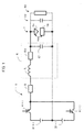
- FIG. 1 An example of a bipolar voltage application circuit used in an embodiment of the present invention is shown in FIG. 1 .
- a bipolar voltage application circuit 9 includes a pair of DC power supplies 3, a pair of switching elements 4, a damping resistance 5, and a feed cable 6.
- Reference symbols 7A and 7B denote a wire electrode and a workpiece, respectively.
- the workpiece 7B is disposed with a predetermined distance from the wire electrode 7A, and a machining gap 7 is formed between the wire electrode 7A and the workpiece 7B.
- the pair of switching elements 4 shown by 4 (+) and 4 (-) in FIG. 1 is on/off controlled by a control circuit (not shown) to switch the DC power supplies 3 shown by 3 (+) and 3 (-) in FIG. 1 , whereby a bipolar AC voltage is applied to the machining gap 7 (see, FIG. 2A ).
- the feed cable 6 in the bipolar voltage application circuit 9 includes an inductance L, a resistance R, and a line-to-line capacitance C1 as physical quantities.
- the machining gap 7 includes a stray capacitance C2 and a leakage resistance R2 as physical quantities, and the stray capacitance C2 and the leakage resistance R2 exist between the opposed surfaces of the electrode 7A and the workpiece 7B. Since a high peak machining current with sharp rising edge is advantageous to rough machining, the bipolar voltage application circuit 9 is constituted so that the impedance of the entire circuit is kept as low as possible. Consequently, although the inductance L and the resistance R are small, the line-to-line capacitance C1 is increased.
- a frequency of an AC high-frequency voltage which can be applied to the machining gap 7 is limited to about 200 to 300 kHz.
- the bipolar voltage application circuit 9 is configured so that the AC high-frequency voltage of not less than 500 kHz can be applied in general.
- the bipolar voltage application circuit 9 configured to be used in the finish machining, when positive and negative voltages are applied to the machining gap 7 while an off time is provided between the application of the positive and negative voltages, charge is first accumulated in the line-to-line capacitance C1 and the stray capacitance C2 during the application of the voltage, and a machining gap voltage Vbb of the machining gap 7 is increased. Thereafter, after entering the off period, the application of the voltage is stopped, whereby the charge accumulated in the line-to-line capacitance C1 and the stray capacitance C2 is discharged through the leakage resistance R2 to gradually reduce the voltage.
- the voltage application period is short and not more than 1 microsecond, an off time is relatively short, and thus the voltage drop during the off period is small and can be almost ignored.
- the machining gap voltage Vbb can have an almost trapezoidal wave shape (see, FIG. 2B ).
- L circuit inductance of, for example, a feed cable
- C the sum of the line-to-line capacitance C1 of the feed cable and the stray capacitance C2 of the machining gap
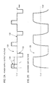
- FIGS. 2A and 2B A power supply output voltage and a machining gap voltage upon switching the DC power supply 3 in the bipolar voltage application circuit 9 of FIG. 1 will be described using FIGS. 2A and 2B .
- a positive voltage 134 and a negative voltage 136 are alternately output, and an off time 132 is provided after each output of the positive voltage 134 and the negative voltage 136.
- the length of time to apply the positive voltage 134 and the negative voltage 136 is represented by ta, and the length of the off time is represented by tb.
- the machining gap voltage between the wire electrode and the workpiece becomes a trapezoidal wave shaped voltage 138 shown in FIG. 2B .
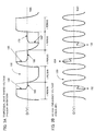
- FIG. 3A shows the machining gap voltage Vbb of a trapezoidal wave shaped voltage 158 used in the present embodiment.
- the machining gap voltages 166, 168, and 170 upon the occurrence of discharge are shown in FIG. 3A .
- FIG. 3B shows the machining gap voltage Vbb of an AC high-frequency voltage 150 (used conventionally) shown in FIG. 11B .
- the machining gap voltages 152, 154, and 156 upon the occurrence of discharge are shown in FIG. 3B .
- the electrostatic attraction force acts between the wire electrode and the workpiece. And so, the wire electrode is bend toward the workpiece by the force, which degrades straightness accuracy.
- the electrostatic attraction force is proportional to the square of the average gap voltage.
- machining gap voltage Vbb of the trapezoidal wave shaped voltage 158 shown in FIG. 3A compared with the machining gap voltage Vbb of the AC high-frequency voltage 150 shown in FIG. 3B , voltage reduction per one discharge is larger. Moreover, as a discharge frequency is increased, the electrostatic attraction force of the wire electrode is rapidly reduced, and straightness accuracy is improved.
- the off times 166, 168, and 170 are reliably provided between individual discharges in the trapezoidal wave shaped voltage 158, whereby a discharge arc is reliably extinguished, and thus individual discharge positions are dispersed to hardly cause discharge concentration. If the concentration of the discharge points occurs, the surface roughness may be degraded.
- This means that determines the change of the machining state includes three-state discrimination signal output means (see, FIG. 4 ), four-state discrimination signal output means (see, FIG. 6 ), and five-state discrimination signal output means (see, FIG. 8 ).
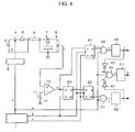
- FIG. 4 is a view for explaining an embodiment of a wire cut electric discharge machine with the three-state discrimination signal output means.
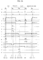
- FIG. 5 is a timing chart showing the operation of the three-state discrimination signal output means shown in FIG. 4 .
- the three-state discrimination signal output means shown in FIG. 4 classifies the machining states into three states of "open”, “discharge”, and “short” and is constituted of a comparator 10, an SR latch 20, first and second D latches 22 and 23, and first, second, and third monostable multi-vibrators 50, 51, and 52.
- the comparator 10, the SR latch 20, the first and second D latches 22 and 23, and the first, second, and third monostable multi-vibrators 50, 51, and 52 are generally used in electronic circuit technology and well-known. For simplification of description, only the case of positive voltage application will be described; however, also in the case of negative voltage application, similar effects can be obtained by a similar constitution just by changing signs.
- a voltage application timing generator 1 is a circuit that outputs a voltage application instruction 'a' for use in the driving of a driver circuit 2 that controls ON/OFF of a switching element 4, outputs a latch instruction 'b' to the SR latch 20 and the D latch circuits 22 and 23 to be described later, and outputs a reset instruction 'c' to the D latch circuits 22 and 23.
- the voltage application instruction 'a' is output from the voltage application timing generator 1 to drive the switching element 4 through the driver circuit 2, and to apply a voltage to the machining gap 7.
- the machining gap voltage Vbb is divided into predetermined voltages by a voltage divider 8 to be input to the first comparator 10.
- a reference voltage V1 of the first comparator 10 is set to be not less than the arc voltage and not more than a power supply voltage E of the DC power supply 3. Specifically, since the machining gap voltage Vbb is divided into the predetermined voltages by the voltage divider 8, the reference voltage V1 is set based on the values of the arc voltage and the DC power supply 3 corresponding to the division ratio.
- An output terminal of the first comparator circuit 10 is connected to an S terminal of the first SR latch 20 and a D terminal of the second D latch 23.
- the first D latch 22 receives an output signal 'i' from a Q terminal ofthefirstSRlatch20, the latch instruction 'b' and the reset instruction 'c' from the voltage application timing generator 1.
- the second D latch 23 receives an output signal 'e' from the first comparator 10, the latch instruction 'b', and the reset instruction ⁇ c'.
- a first AND gate 30 receives an output signal 'f' from the second D latch 23 and the voltage application instruction ⁇ a' from the voltage application timing generator 1, and a second AND gate 31 receives an output signal 'j' from the first D latch 22 and the voltage application instruction 'a' from the voltage application timing generator 1.
- the first monostable multi-vibrator 50 receives an output signal 'g' from the first AND gate 30 and outputs an output signal 'h' from the first monostable multi-vibrator 50.
- the third monostable multi-vibrator 52 receives an output signal 'k' from the second AND gate 31 and outputs an output signal 'l' from the third monostable multi-vibrator52 .
- the output signals 'h' and 'l' respectively from the first and third monostable multi-vibrators 50 and 52 are respectively input to first and second inverters 40 and 41.
- the output signals 'h' and 'l' are inverted respectively by the first and second inverters 40 and 41, and then output signals 'm' and 'n' as inversion signals are output from the first and second inverters 40 and 41.
- the output signals 'm' and 'n' and the voltage application instruction 'a' are input to a three-input AND gate 36, and an output signal 'o' from the three-input AND gate 36 is input to the second monostable multi-vibrator 51.
- the second monostable multi-vibrator 51 outputs an output signal 'p'.
- the output signal 'h' is used as a signal (that is, an open signal 'h') for use in the determination of whether or not the machining gap 7 is in an open state.
- the output signal 'p' is used as a signal (that is, a discharge signal 'p') for use in the determination of whether or not the machining gap 7 is in a discharge state.
- the output signal 'l' isusedasasignal (that is, a short signal 'l') for use in the determination of whether or not the machining gap 7 is in a short state.
- the open signal 'h', the discharge signal 'p', and the short signal 'l' are counted by a counting circuit (not shown).
- the output signal 'd' of the voltage divider 8 is more than the reference voltage V1 of the first comparator 10
- the output signal 'e' of the first comparator 10 is changed from low level to high level.
- the first SR latch 20 is then set with the output signal 'e'. Consequently, a Q output 'i' of the first SR latch 20 is changed from low level to high level.
- the low and high levels respectively mean low and high potentials in an operating voltage of an electronic circuit.
- the voltage application instruction 'a' of the voltage application timing generator 1 is returned to OFF (see, 'a2')
- the charge accumulated in the stray capacitance C2 of the machining gap 7 remains. Therefore, the machining gap voltage Vbb is gradually reduced as long as no discharge occurs in the machining gap 7, and the output signals 'd', 'e', and 'i' are not changed.
- the latch instruction 'b' is output from the voltage application timing generator 1 to the first SR latch 20, the first D latch 22, and the second D latch 23 immediately before the next voltage application instruction 'a' (see, 'a3').
- the latch instruction 'b' is input to a reset terminal of the first SR latch 20, a CK terminal of the first D latch 22, and a CK terminal of the second D latch 23.
- the output 'e' of the first comparator 10 is held in the second D latch 23, and the output 'i' of the first SR latch 20 is held in the first D latch 22.
- the output signal 'j' of a *Q terminal of the first D latch 22 is changed from high level to low level, and, at the same time, the first SR latch 20 is reset.
- the output 'i' of the first SR latch 20 is temporarily dropped to a low level, the output 'e' of the first comparator 10 is kept in a high level state, and therefore the output 'i' of the first SR latch 20 is immediately set to return to a high level.
- the output ⁇ f' of the second D latch 23 is also high level. Therefore, the output 'g' of the first AND gate 30 is also high level to trigger the first monostable multi-vibrator 50, and to output the open signal 'h'. Meanwhile, since the output signal 'j' of the *Q terminal of the first D latch 22 is low level, the output signal 'k' of the second AND gate 31 is held at a low level, and the short signal 'l' is not output from the third monostable multi-vibrator 52 (namely, the short signal 'l' is held at a low level).
- the open signal 'h' from the secondmonostable multi-vibrator 51 reaches a high level, the input 'm' of the three-input AND gate 36 is dropped to a low level. The output 'o' is held at a low level. The second monostable multi-vibrator 51 is thus not triggered, and the discharge signal 'p' is not output from the second monostable multi-vibrator 51.
- the reset instruction 'c' is then output simultaneously with OFF of the voltage application instruction 'a' from the voltage application timing generator 1 (see, 'a4'), and the first and second D latches 22 and 23 are reset.
- the output 'j' of the *Q terminal of the first D latch 22 is returned to a high level
- the output 'f' of the Q terminal of the second D latch 23 is returned to a low level.
- the machining gap voltage Vbb drops near the arc voltage at once (see, 'd1'), and the output 'e' of the first comparator 10 is returned to a low level.
- the switching element 4 since the switching element 4 is already turned off, the voltage does not increase even if the discharge is terminated, and the machining gap voltage Vbb is kept at not more than the arc voltage.
- the latch instruction 'b' is output immediately before the next voltage application instruction 'a' from the voltage application timing generator 1 (see, 'a5')
- the output 'e' of the first comparator 10 is low level, and therefore, the Q output 'f' of the second D latch 23 is also low level.
- the output 'i' of the first SR latch 20 is held at a high level, the output signal 'j' of the *Q terminal of the first D latch 22 is dropped to a low level as in the previous time.
- the open signal 'h' and the short signal 'l' are input respectively to the inverters 40 and 41. Therefore, the inversion signals 'm' and 'n' are high level, and the voltage application instruction 'a' is high level. Thus, the output signal 'o' of the three-input AND gate 36 is high level to trigger the second monostable multi-vibrator 51, and to output the discharge signal 'p'.
- the machining gap 7 is in a short state, and when the output 'd' of the voltage divider 8 is less than the reference voltage V1 of the first comparator 10, the first SR latch 20 is not set, and the output signal 'i' is held at a low level. In that case, the output 'j' of the *Q terminal of the first D latch 22 is held at a high level and is not changed. Moreover, since the output signal ⁇ f' of the Q terminal of the second D latch 23 is low level, only the output 'k' of the second AND gate 31 is high level (see, 'k1'), and the short signal 'l' is output from the third monostable multi-vibrator 52 (see, ⁇ 11').
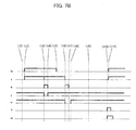
- FIG. 6 is a view for explaining an embodiment of a wire cut electric discharge machine with the four-state discrimination signal outputmeans.
- FIGS. 7A and 7B are timing charts showing the operation of the four-state discrimination signal output means shown in FIG. 6 .
- the four-state discrimination signal output means shown in FIG. 6 classifies the "discharge” state in more detail into “discharge” and “immediate discharge”, whereby the entire machining state is classified into four states of "open”, “discharge”, “immediate discharge”, and "short".
- the four-state discrimination signal output means shown in FIG. 6 includes the components of the three-state discrimination signal output means shown in FIG. 4 , a second comparator 12, a second SR latch 21, a third D latch 24, a four-input AND gate 33, a fourth monostable multi-vibrator 53, and a fifth monostable multi-vibrator 54.
- the four-state discrimination signal output means uses a three-input AND gate 32 instead of the three-input AND gate 36, uses the fourth monostable multi-vibrator 53 instead of the second monostable multi-vibrator 51, and includes a third inverter 42 added as an input of the four-input AND gate 33 inputting the signal to the fifth monostable multi-vibrator 54.
- the voltage application instruction 'a' is output from the voltage application timing generator 1 to drive the switching element 4 through the driver circuit 2, and thus a voltage based on the power supply voltage E of the DC power supply 3 is applied to the machining gap 7.
- the machining gap voltage Vbb is divided into predetermined voltages by the voltage divider 8 to be input to the first and second comparators 10 and 12.
- the reference voltage V1 of the first comparator 10 is set to be not less than the arc voltage
- a reference voltage V2 of the second comparator 12 is set to a value lower than the power supply voltage E and considering the voltage drop of the machining gap voltage Vbb during the off time (see, FIG. 2A ). Since the machining gap voltage Vbb is divided into the predetermined voltages by the voltage divider 8, the reference voltages V1 and V2 are set based on values corresponding to the division ratio.
- the machining gap voltage Vbb is increased, and when the output signal 'd' of the voltage divider 8 is more than the reference voltage V1 of the first comparator 10, the output signal 'e' of the first comparator 10 is changed from low level to high level.
- the first SR latch 20 is then set with the output signal 'e'. Consequently, the output signal 'i' of the Q terminal of the first SR latch 20 is changed from low level to high level.
- the machining gap voltage Vbb is increased, and when the output signal 'd' of the voltage divider 8 is more than the reference voltage V2 of the second comparator 12, an output signal 'q' of the second comparator 12 is changed from low level to high level, and likewise, the second SR latch 21 is set. Consequently, an output signal 'r' of a Q terminal of the second SR latch 21 is changed from low level to high level.
- the latch instruction 'b' is output from the voltage application timing generator 1 immediately before the next voltage application instruction 'a'
- the output signal 'e' of the first comparator 10 is held in the second D latch 23, and the output signal 'i' of the Q terminal of the first SR latch 20 is held in the first D latch 22.
- the output signal 'j' of the *Q terminal of the first D latch 22 is changed from high level to low level, and, at the same time, the first SR latch 20 is reset.
- the output signal 'i' of the Q terminal of the first SR latch 20 is temporarily dropped to a low level, the output of the first comparator 10 is held at a high level, and therefore the output signal 'i' of the first SR latch 20 is immediately set to return to a high level.
- the output signal 'r' of the Q terminal of the second SR latch 21 is held in the third D latch 24, and, at the same time, the second SR latch 21 is reset; however, since the output of the second comparator 12 is held at a high level, the output signal 'r' is immediately set again.
- the output signal 'f' of the Q terminal of the second D latch 23 is also high level, and therefore, the output signal 'g' of the first AND gate 30 is also high level.
- the output signal 'g' triggers the first monostable multi-vibrator 50 to output the open signal 'h'.
- the output signal 't' of a *Q terminal of the second D latch 23 is low level, the output signal 'o'' of the three-input AND gate 32 is low level, and consequently, a discharge signal 'p'' is not output from the fourthmonostable multi-vibrator 53.
- the inversion signal 'm' is low level.
- the output signal 'v' of the four-input AND gate 33 is held at a low level, and an immediate discharge signal 'w' is not output from the fifth monostable multi-vibrator 54.
- the reset instruction 'c' is then output simultaneously with OFF of the voltage application instruction 'a' from the voltage application timing generator 1, and the first, second, and third D latches 22, 23, and 24 are reset.
- the output signal ⁇ j' of the *Q terminal of the first D latch 22 is returned to a high level
- the output signal 'f' of the Q terminal of the second D latch 23 is returned to a low level
- the output signal 't' of the *Q terminal is returned to a high level
- the output signal 's' of the Q terminal of the third D latch 24 is returned to a low level.
- the machining gap voltage Vbb drops near the arc voltage at once, and the output signal 'e' of the first comparator 10 and the output signal 'q' of the second comparator 12 are returned to low levels.
- the switching element 4 since the switching element 4 is already turned off, the voltage does not increase even if the discharge is terminated, and the machining gap voltage Vbb is kept at not more than the arc voltage.
- the output signal 'e' of the first comparator 10 is low level; therefore, the output signal 'f' of the Q terminal of the second D latch 23 is low level, and the output signal 't' of the *Q terminal is high level.
- the output signal 'i' of the first SR latch 20 and the output signal 'r' of the second SR latch 21 are held at a high level, the output signal 'j' of the *Q terminal of the first D latch 22 is low level, and the output signal 's' of the Q terminal of the third D latch 24 is high level.
- the output signal 'f' from the Q terminal of the second D latch 23 and the output signal 'j' from the *Q terminal of the first D latch 22 are low level this time.
- the output signals' from the Q terminal of the third D latch 24 and the output signal 't' from the *Q terminal of the second D latch 23 are high level. Therefore, the output signal 'g' of the first AND gate 30 and the output signal 'k' of the second AND gate 31 are low level, and only the output signal 'o'' of the three-input AND gate 32 is high level.
- the discharge signal 'p'' is output from the fourth monostable multi-vibrator 53.
- the machining gap 7 is in a short state, and when the output signal 'd' of the voltage divider 8 is less than the reference voltage V1 of the first comparator 10, the output signals 'e' and 'q' from the first and second comparators 10 and 12 are held at a low level.
- the first and second SR latches 20 and 21 are not set, and the output signals 'i' and 'r' are held at a low level. In that case, only the output signal 'j' of the *Q terminal of the first D latch 22 and only the output signal 't' of the *Q terminal of the second D latch 23 are high level.
- the voltage application instruction 'a' is high level
- only the output signal 'k' of the second AND gate 31 is high level, and the short signal 'l' is output.
- the output signal 'd' of the voltage divider 8 is more than the reference voltage V1 of the first comparator 10, and the first SR latch 20 is set. Thereafter, when discharge occurs before reaching the reference voltage V2 of the second comparator 12, eventually only the output signal 't' of the *Q terminal of the second D latch 23 is high level. Therefore, the output signals 'g', 'k', and 'o'' of the first, second, and third AND gates 30, 31, and 32 are low level, and the open signal 'h', the discharge signal 'p'', the short signal '1' are not output from the first, fourth, and thirdmonostable multi-vibrators 50, 53, and 52.
- the respective inversion signals 'm', 'n', and 'u' of the output signals 'h', '1', and 'p'' are high level
- the output signal 'v' of the four-input AND gate 33 is high level
- the immediate discharge signal 'w' is output from the fifth monostable multi-vibrator 54.
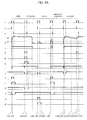
- FIG. 8 is a view for explaining an embodiment of a wire cut electric discharge machine with the five-state discrimination signal output means.
- FIGS. 9A and 9B are timing charts showing the operation of the five-state discrimination signal output means shown in FIG. 8 .
- the five-state discrimination signal output means shown in FIG. 8 uses a fourth D latch 25, an AND gate 38, and a seventh monostable multi-vibrator 56 instead of the second D latch 23, the first AND gate 30, and the first monostable multi-vibrator 50 of the four-state discrimination signal output means shown in FIG. 6 .
- the five-state discrimination signal output means further includes a three-input AND gate 37 and an eighth monostable multi-vibrator 57.
- the five-state discrimination signal output means uses a five-input AND gate 35 and a ninth monostable multi-vibrator 58 instead of the four-input AND gate 33 and the fifth monostable multi-vibrator 54 of FIG. 6 .
- the fourth D latch 25 holding the output signal 'q' of the second comparator 12 and a leakage signal output circuit are added, and the open discrimination circuit is changed; however, the other discrimination outputs are the same as those of the four-state discrimination signal output means.
- the output signal 'h'' represents an open state
- 'p'' represents a discharge state
- ' ⁇ ' represents a leakage state
- 'l' represents a short state
- 'w'' represents an immediate discharge state.
- the switching element 4 is turned on based on the voltage application instruction 'a' from the voltage application timing generator 1, the machining gap voltage Vbb is increased, and the output signal 'd' of the voltage divider 8 is more than the respective levels of the reference voltages V1 and V2 of the first and second comparators 10 and 12.
- the first and second SR latches 20 and 21 are set, and the output signal 'i' from the first SR latch 20 and the output signal 'r' from the second SR latch 21 are high level.
- all D latches including the first to fourth D latches 22 to 25 set a high level signal by the output of the latch instruction 'b' immediately before the application instruction from the voltage application instruction 'a' from the voltage application timing generator 1. Consequently, the output signals 'f' , 's', and 'x' of the Q terminals of the second, third, and fourth D latches 23, 24, and 25 are high levels, and the output signals 'j', 't', and 'y' of the *Q terminals of the first, second, and fourth D latches 22, 23, and, 25 are low levels. Therefore, when the voltage application instruction 'a' is high level, only the output signal 'g'' of the AND gate 38 is high level, and the open signal 'h'' is output from the seventh monostable multi-vibrator 56.
- the output signal 'd' from the voltage divider 8 is more than the respective levels of the reference voltages V1 and V2 of the first and second comparators 10 and 12 by virtue of the application of voltage to the machining gap 7, the output signal 'd' is then gradually reduced, and when the next latch instruction 'b' is output, the output signal 'd' is reduced to not more than the level of the reference voltage V2.
- the first and second SR latches 20 and 21 are set, and since the output signal 'e' of the first comparator 10 is high level, the first, second, and third D latches 22, 23, and 24 set a high level signal. However, since the output signal 'q' of the second comparator 12 is low level, only the fourth D latch 25 sets a low level signal.
- the output signal 'f' of the Q terminal of the second D latch 23, the output signal 's' of the Q terminal of the third D latch 24, and the output signal 'y' of the *Q terminal of the fourth D latch 25 are high level.
- the output signal 'j' of the *Q terminal of the first D latch 22, the output signal 't' of the *Q terminal of the second D latche 23, and the output signal 'x' of the *Q terminal of the fourth D latch 25 are low level.
- such a case is considered that although the output signal 'd' of the voltage divider 8 is more than the reference voltage V1 of the first comparator 10 by virtue of the application of voltage to the machining gap 7, it does not reaches the reference voltage V2 of the second comparator 12, and the next latch instruction 'b' is output while this state is maintained (in other words, a case in which the output signal 'd' is maintained between the reference values V1 and V2).
- the first SR latch 20 is set, and since the output signal 'e' of the first comparator 10 is high level, the first and second D latches 22 and 23 set a high level signal.
- the second SR latch 21 is not set, and since the output signal 'q' of the second comparator 12 is low level, the third and fourth D latches 24 and 25 set a low level signal.
- the output signal 'f' of the Q terminal of the second D latch 23 and the output signal 'y' of the *Q terminal of the fourth D latch 25 are high level, and the output signal 'j' of the Q terminal of the first D latch 22, the output signal 's' of the Q terminal of the third D latch 24, the output signal 't' of the *Q terminal of the second D latch 23, and the output signal 'x' of the Q terminal of the fourth D latch 25 are low level.
- the voltage application instruction 'a' is high level, only the output signal 'z' of the AND gate 37 is high level again, and the leakage signal ' ⁇ ' is output from the eighthmonostable multi-vibrator 57.
- FIG. 10 is a block diagram of the relevant portion of a controller of the wire cut electric discharge machine in one embodiment of the present invention.
- a controller 80 includes a CPU 81, and a memory 82 constituted of a ROM and a RAM, a display 83, input device 84 such as a keyboard, an interface 85 which inputs or outputs a machining program and so on from an external storage medium, respective axe control means 86, machining fluid flow rate control means 88 that controls the flow rate of a machining fluid, and a power circuit 98, which are connected to the CPU 81 through a bus 89.
- a guide position of a work table and a wire electrode is controlled by the respective axes control means 86, and consequently, the position and speed of the wire electrode relative to the work table are determined.
- the power circuit 98 has been described using FIGS. 4 , 6 , and 8 and includes a voltage application circuit that applies voltage to a machining gap, a various-state detection circuit, and a counting circuit.
- the respective axes control means 86 controls motors respectively driving X, Y, Z, U, and V axes and includes feedback control means for the position of each axis (X, Y, Z, U, and V axes), the speed, and the current.
- a table (not shown) on which the workpiece 7B (see, FIG. 1 ) is placed is driven in X-axis and Y-axis directions perpendicular to each other.
- an upper guide is moved in a direction perpendicular to the X and Y axes.
- the U and V axes are used for taper machining and perpendicular to each other.
- the respective axes control means 86 is connected to a servo motor 94 for each axis through a servo amp 90 for each axis.
- the servomotors 94 each include a position/speed detector, so that position and speed are fed back to respective axis control circuits. However, the description about the feedback is omitted in FIG. 10 .
- the power circuit 98 transmits to the controller 80 results obtained by counting three-state discrimination signals, four-state discrimination signals, or five-state discrimination signals for a predetermined time by means of the counting circuit.
- the controller 80 based on the counting result of each state transmitted from the power circuit 98, the counting is performed for a longer time if necessary to detect a trend in each state, and to obtain state discrimination data.
- the controller 80 compares the state discrimination data with previously-set reference data to thereby control a relative feed speed of the wire electrode 7A with respect to the workpiece 7B, control the off time of the power supply voltage, regulate the flow rate of the machining fluid, and change a set value of the positive and negative power supply voltages.
- the machining state of the machining gap 7 can be analogized more directly and in more detail than the prior art using an average voltage. For example, even when the leakage state, number of times of discharging, or number of times of short is increased, the average voltage drops. Thus, although it is hard to determine what are the reasons from the average voltage, the reason can be clearly determined in the case of the present invention, and a suitable response can be given as described later.
- the state is frequently shifted during machining due to the influences of a vibration state of a wire and a retention state of machining sludge, and therefore, if the machining state is tobe directly controlled based on individual results obtained for each voltage application, a system is vibrated to easily lose stability. Thus, it is empirically found that the machining state can be controlled better byperforming a control operation based on a number of results, for example, several tens to several hundreds of results.
Landscapes
- Engineering & Computer Science (AREA)
- Mechanical Engineering (AREA)
- Electrical Discharge Machining, Electrochemical Machining, And Combined Machining (AREA)
Claims (7)
- Elektrische Drahterodiermaschine, die eine Hochfrequenzspannung anlegt an eine Bearbeitungslücke (7) zwischen einer Drahtelektrode (7A) und einem Arbeitsstück (7B), angeordnet an einer vorbestimmten Entfernung von der Drahtelektrode, zum Erzeugen einer Entladung, und zum Bearbeiten des Arbeitsstücks, umfassend
bipolare Spannungsanlegemittel (9), ausgelegt zum Anlegen einer Spannung (130) mit abwechselnd positiver (134) und negativer (136) Polarität an die Bearbeitungslücke (7) mit einer Periode (Tc) von nicht mehr als 1 Mikrosekunde und einer Auszeit (132; tb) zwischen einzelnen Spannungsanlegen von mindestens nicht geringer als die Anlegezeit (ta), so dass eine Bearbeitungslückenspannung (Vbb) eine trapezförmige Wellenform hat;
Bearbeitungslückenspannung-Erfassungsmittel, ausgelegt zum Erfassen der in der Bearbeitungslücke (7) erzeugten Bearbeitungslückenspannung (Vbb);
Diskriminationssignal-Ausgabemittel (98), ausgelegt zum, auf der Basis der vom Bearbeitungslückenspannung-Erfassungsmittel erfassten Bearbeitungslückenspannung (Vbb), Klassifizieren von Bearbeitungszuständen in drei Zustände "offen", "Entladung" und "kurz" für jede Spannungsanlage, ausgeführt durch das Spannungsanlegemittel (9), und zum Ausgeben eines Zustanddiskriminationssignals, entsprechend jedem dieser Zustände; und
Zählmittel (98), ausgelegt zum Zählen jedes der vom Diskriminationssignal-Ausgabemittel (98) ausgegebenen Zustanddiskriminationssignale zum Erhalten von Zustanddiskriminationsdaten. - Elektrische Drahterodiermaschine gemäß Anspruch 1, wobei das Diskriminationssignal-Ausgabemittel (98) eine Diskriminationsstufe hat, deren absoluter Wert nicht mehr als eine Leerlaufspannung und nicht geringer als eine Lichtbogenspannung ist, und im Timing vom Beginnen des Spannungsanlegens an die Bearbeitungslücke (7),
das Diskriminationssignal-Ausgabemittel (98) ausgelegt ist zum Ausgeben eines "offen"-Signals, ist der absolute Wert der Bearbeitungslückenspannung (Vbb) nicht geringer als die Diskriminationsstufe,
das Diskriminationssignal-Ausgabemittel (98) ausgelegt ist zum Ausgeben eines "kurz"-Signals, hat der absolute Wert seit dem Beginn des letzten Spannungsanlegens nie die Diskriminationsstufe überstiegen, und
das Diskriminationssignal-Ausgabemittel (98) ausgelegt ist zum Ausgeben eines "Entladung"-Signals, in Fällen, die nicht irgendeinem der oben genannten Fälle entsprechen. - Elektrische Drahterodiermaschine gemäß Anspruch 1, wobei das Diskriminationssignal-Ausgabemittel (98) ausführbar ist zum Klassifizieren von Bearbeitungszuständen in vier Zustände "offen", "Entladung", "sofortige Entladung" und "kurz" für jedes vom Spannungsanlegemittel (9) ausgeführte Spannungsanlegen.
- Elektrische Drahterodiermaschine gemäß Anspruch 3, wobei das Diskriminationssignal-Ausgabemittel (98) zwei Diskriminationsstufen hat, einschließlich hohe und niedrige Stufe, deren absoluter Wert nicht mehr als eine Leerlaufspannung und nicht geringer als eine Lichtbogenspannung ist, und im Timing vom Beginnen des Spannungsanlegens an die Bearbeitungslücke (7),
das Diskriminationssignal-Ausgabemittel (98) ausgelegt ist zum Ausgeben eines "offen"-Signals, ist der absolute Wert der Bearbeitungslückenspannung (Vbb) nicht geringer als die hohe Stufe,
das Diskriminationssignal-Ausgabemittel (98) ausgelegt ist zum Ausgeben eines "kurz"-Signals, hat der absolute Wert seit dem Beginn des letzten Spannungsanlegens nie die niedrige Stufe überstiegen,
das Diskriminationssignal-Ausgabemittel (98) ausgelegt ist zum Ausgeben eines "Entladungs"-Signals, hat der absolute Wert seit dem Beginn des letzten Spannungsanlegens einmal die hohe Stufe überstiegen und ist er nicht höher als die niedrige Stufe zum Zeitpunkt des nächsten Spannungsanlegens, und
das Diskriminationssignal-Ausgabemittel (98) ausgelegt ist zum Ausgeben eines "sofortige Entladungs"-Signals, in Fällen, die nicht irgendeinem der oben genannten Fälle entsprechen. - Elektrische Drahterodiermaschine gemäß Anspruch 1, wobei das Diskriminationssignal-Ausgabemittel (98) ausführbar ist zum Klassifizieren von Bearbeitungszuständen in fünf Zustände "offen", "Ableitung", "Entladung", "sofortige Entladung" und "kurz" für jedes vom Spannungsanlegemittel (9) ausgeführte Spannungsanlegen.
- Elektrische Drahterodiermaschine gemäß Anspruch 5, wobei das Diskriminationssignal-Ausgabemittel (98) zwei Diskriminationsstufen hat, einschließlich hohe und niedrige Stufe, deren absoluter Wert nicht mehr als eine .Leerlaufspannung und nicht geringer als eine Lichtbogenspannung ist, und im Timing vom Beginnen des Spannungsanlegens an die Bearbeitungslücke (7),
das Diskriminationssignal-Ausgabemittel (98) ausgelegt ist zum Ausgeben eines "offen"-Signals, ist der absolute Wert der Bearbeitungslückenspannung (Vbb) nicht geringer als die hohe Stufe,
das Diskriminationssignal-Ausgabemittel (98) ausgelegt ist zum Ausgeben eines "Entladungs"'Signals, ist die Bearbeitungslückenspannung (Vbb) nicht höher als die hohe Stufe und nicht geringer als die niedrige Stufe,
das Diskriminationssignal-Ausgabemittel (98) ausgelegt ist zum Ausgeben eines "kurz"-Signals, hat der absolute Wert seit dem Beginn des letzten Spannungsanlegens nie die geringe Stufe überstiegen,
das Diskriminationssignal-Ausgabemittel (98) ausgelegt ist zum Ausgeben eines "Entladungss"-Signals, hat der absolute Wert seit dem Beginn des letzten Spannungsanlegens einmal die hohe Stufe überstiegen und ist er nicht höher als die niedrige Stufe zum Zeitpunkt des nächsten Spannungsanlegens, und
das Diskriminationssignal-Ausgabemittel (98) ausgelegt ist zum Ausgeben eines "sofortige Entladungss"-Signals, in Fällen, die nicht irgendeinem der oben genannten Fälle entsprechen. - Elektrische Drahterodiermaschine gemäß irgendeinem der Ansprüche 1, 3 und 5, wobei die elektrische Drahterodiermaschine ausführbar ist zum Vergleichen mindestens eines Werts der vom Zählmittel (98) erhaltenen Zustanddiskriminationsdaten mit einem vorher eingestellten Referenzwert, und zum Ändern von mindestens einem aus der Zufuhrgeschwindigkeit der Drahtelektrode (7A), der Länge der Auszeit (132; tb), der Flussgeschwindigkeit eines Bearbeitungsfluids, und eines eingestellten Werts einer positiven und negativen Energiezufuhrspannung des Spannungsanlegemittels (9).
Applications Claiming Priority (1)
| Application Number | Priority Date | Filing Date | Title |
|---|---|---|---|
| JP2009136605A JP4648468B2 (ja) | 2009-06-05 | 2009-06-05 | 加工状態判定機能を備えたワイヤカット放電加工機 |
Publications (3)
| Publication Number | Publication Date |
|---|---|
| EP2269755A2 EP2269755A2 (de) | 2011-01-05 |
| EP2269755A3 EP2269755A3 (de) | 2012-10-10 |
| EP2269755B1 true EP2269755B1 (de) | 2014-06-25 |
Family
ID=43126954
Family Applications (1)
| Application Number | Title | Priority Date | Filing Date |
|---|---|---|---|
| EP10164081.1A Active EP2269755B1 (de) | 2009-06-05 | 2010-05-27 | Elektrische Drahterodiermaschine mit Funktion zur Unterscheidung des mechanischen Bearbeitungsstatus |
Country Status (4)
| Country | Link |
|---|---|
| EP (1) | EP2269755B1 (de) |
| JP (1) | JP4648468B2 (de) |
| CN (1) | CN101905360B (de) |
| TW (1) | TWI436843B (de) |
Families Citing this family (19)
| Publication number | Priority date | Publication date | Assignee | Title |
|---|---|---|---|---|
| CN102601472B (zh) * | 2011-01-19 | 2015-08-26 | 通用电气公司 | 放电加工系统及方法 |
| JP5166586B1 (ja) | 2011-10-13 | 2013-03-21 | ファナック株式会社 | 加工状態に基づき加工液量を調節するワイヤ放電加工機 |
| JP5204321B1 (ja) | 2012-02-01 | 2013-06-05 | ファナック株式会社 | 加工状態を検出し極間の平均電圧を求めるワイヤ放電加工機 |
| CN103240474B (zh) * | 2012-02-13 | 2018-07-10 | 严政 | 一种电火花加工设备放电间隙控制方法 |
| CN102890220A (zh) * | 2012-07-05 | 2013-01-23 | 宁波虎兴数控科技有限公司 | 一种用于线切割机床连线测试的系统 |
| JP5930913B2 (ja) * | 2012-08-10 | 2016-06-08 | 三菱電機株式会社 | ワイヤ放電加工装置 |
| JP5642810B2 (ja) * | 2013-01-08 | 2014-12-17 | ファナック株式会社 | 放電加工用電源装置 |
| JP5739563B2 (ja) | 2013-07-24 | 2015-06-24 | ファナック株式会社 | 平均放電遅れ時間算出手段を備えたワイヤ放電加工機 |
| CN103962659B (zh) * | 2014-05-13 | 2017-02-15 | 东莞华中科技大学制造工程研究院 | 一种电火花加工控制方法 |
| JP6230481B2 (ja) * | 2014-05-15 | 2017-11-15 | 三菱電機株式会社 | マルチワイヤ放電加工装置 |
| JP6063068B2 (ja) * | 2015-04-02 | 2017-01-18 | ファナック株式会社 | ワイヤ放電加工機 |
| EP3085482B1 (de) | 2015-04-02 | 2022-02-09 | Fanuc Corporation | Drahterosionsmaschine |
| JP6227599B2 (ja) | 2015-08-25 | 2017-11-08 | ファナック株式会社 | 極間距離を一定にするワイヤ放電加工機 |
| JP6426770B2 (ja) * | 2017-02-06 | 2018-11-21 | ファナック株式会社 | サーボ制御装置 |
| CN107322109B (zh) * | 2017-08-17 | 2023-04-25 | 江苏冬庆数控机床有限公司 | 抑制/消除电火花穿孔加工表面孔口翻边的电路及方法 |
| JP6945489B2 (ja) * | 2018-04-27 | 2021-10-06 | 三菱電機株式会社 | マルチワイヤ放電加工装置 |
| CN109202192B (zh) * | 2018-10-31 | 2019-09-17 | 清华大学 | 微细电火花伺服扫描加工参数优选方法及系统 |
| JP6883138B1 (ja) * | 2020-09-03 | 2021-06-09 | 株式会社ソディック | 放電加工機 |
| CN115156648B (zh) * | 2022-07-15 | 2024-10-11 | 歌尔股份有限公司 | 模具加工方法、设备及计算机可读存储介质 |
Citations (1)
| Publication number | Priority date | Publication date | Assignee | Title |
|---|---|---|---|---|
| US20050127041A1 (en) * | 2002-06-12 | 2005-06-16 | Hiroatsu Kobayashi | Electric power unit for machining of wire electric discharge machine |
Family Cites Families (16)
| Publication number | Priority date | Publication date | Assignee | Title |
|---|---|---|---|---|
| US3705286A (en) * | 1971-01-21 | 1972-12-05 | Iwao Kondo | Electric discharge machining device |
| JPS5596228A (en) * | 1979-01-08 | 1980-07-22 | Hitachi Seiko Ltd | Discharge working method |
| JPS5748424A (en) * | 1980-09-03 | 1982-03-19 | Hitachi Seiko Ltd | Control system for electric discharge machine |
| JPS59205223A (ja) * | 1983-05-02 | 1984-11-20 | Mitsubishi Electric Corp | 放電加工装置 |
| JPS61260915A (ja) | 1985-05-15 | 1986-11-19 | Mitsubishi Electric Corp | 放電加工用電源 |
| EP0372036A1 (de) * | 1988-05-16 | 1990-06-13 | Charmilles Technologies S.A. | Vorrichtung und verfahren zur permanentadaptiv-regelung für edm-drahtschneidemaschinen |
| JPH0475822A (ja) * | 1990-07-12 | 1992-03-10 | I N R Kenkyusho:Kk | 放電加工装置 |
| JP2939310B2 (ja) * | 1990-08-14 | 1999-08-25 | 株式会社ソディック | 放電加工装置 |
| JP3293416B2 (ja) * | 1994-08-09 | 2002-06-17 | 三菱電機株式会社 | 放電加工機の放電状態検出装置 |
| JPH0911043A (ja) * | 1995-06-29 | 1997-01-14 | Nec Corp | 放電加工方法及び放電加工装置 |
| JP2000079514A (ja) * | 1998-09-01 | 2000-03-21 | Mitsubishi Electric Corp | 放電加工装置 |
| JP3795799B2 (ja) | 2000-12-25 | 2006-07-12 | ファナック株式会社 | ワイヤ放電加工機の制御装置 |
| US7038158B2 (en) * | 2002-08-30 | 2006-05-02 | Mitsubishi Denki Kabushiki Kaisha | Wire electrical discharge machining apparatus |
| GB0504600D0 (en) * | 2005-03-04 | 2005-04-13 | Univ Strathclyde | Detecting partial discharge in high voltage cables |
| JP2007044813A (ja) * | 2005-08-10 | 2007-02-22 | Fanuc Ltd | 放電加工装置 |
| CN100427961C (zh) * | 2006-09-20 | 2008-10-22 | 重庆大学 | 基于虚拟仪器技术的气体绝缘组合电器在线监测方法 |
-
2009
- 2009-06-05 JP JP2009136605A patent/JP4648468B2/ja active Active
-
2010
- 2010-04-28 TW TW99113520A patent/TWI436843B/zh active
- 2010-05-27 EP EP10164081.1A patent/EP2269755B1/de active Active
- 2010-06-04 CN CN2010101988443A patent/CN101905360B/zh active Active
Patent Citations (1)
| Publication number | Priority date | Publication date | Assignee | Title |
|---|---|---|---|---|
| US20050127041A1 (en) * | 2002-06-12 | 2005-06-16 | Hiroatsu Kobayashi | Electric power unit for machining of wire electric discharge machine |
Also Published As
| Publication number | Publication date |
|---|---|
| TW201102199A (en) | 2011-01-16 |
| JP2010280046A (ja) | 2010-12-16 |
| JP4648468B2 (ja) | 2011-03-09 |
| CN101905360B (zh) | 2012-07-04 |
| TWI436843B (zh) | 2014-05-11 |
| CN101905360A (zh) | 2010-12-08 |
| EP2269755A3 (de) | 2012-10-10 |
| EP2269755A2 (de) | 2011-01-05 |
Similar Documents
| Publication | Publication Date | Title |
|---|---|---|
| EP2269755B1 (de) | Elektrische Drahterodiermaschine mit Funktion zur Unterscheidung des mechanischen Bearbeitungsstatus | |
| EP2505293B1 (de) | Elektrische Drahterodiermaschine mit Funktion zur Erfassung des Bearbeitungszustands | |
| JP5204321B1 (ja) | 加工状態を検出し極間の平均電圧を求めるワイヤ放電加工機 | |
| JP5739563B2 (ja) | 平均放電遅れ時間算出手段を備えたワイヤ放電加工機 | |
| EP2223764B1 (de) | Drahtfunkenerosionsmaschine | |
| US20130024020A1 (en) | Numerical control device, wire electric discharge machining apparatus using the same, and wire electric discharge machining method using the same | |
| JP4833197B2 (ja) | 放電加工機の電源制御装置 | |
| JP4833198B2 (ja) | 放電加工機の電源制御装置 | |
| CN103909313B (zh) | 电火花加工用电源装置 | |
| EP3085482A2 (de) | Drahterosionsmaschine | |
| JP5357298B2 (ja) | 加工状態を検出するワイヤ放電加工機 | |
| CN104837588B (zh) | 放电加工装置 | |
| CN104837588A (zh) | 放电加工装置 |
Legal Events
| Date | Code | Title | Description |
|---|---|---|---|
| PUAI | Public reference made under article 153(3) epc to a published international application that has entered the european phase |
Free format text: ORIGINAL CODE: 0009012 |
|
| AK | Designated contracting states |
Kind code of ref document: A2 Designated state(s): AL AT BE BG CH CY CZ DE DK EE ES FI FR GB GR HR HU IE IS IT LI LT LU LV MC MK MT NL NO PL PT RO SE SI SK SM TR |
|
| AX | Request for extension of the european patent |
Extension state: BA ME RS |
|
| RAP1 | Party data changed (applicant data changed or rights of an application transferred) |
Owner name: FANUC CORPORATION |
|
| PUAL | Search report despatched |
Free format text: ORIGINAL CODE: 0009013 |
|
| AK | Designated contracting states |
Kind code of ref document: A3 Designated state(s): AL AT BE BG CH CY CZ DE DK EE ES FI FR GB GR HR HU IE IS IT LI LT LU LV MC MK MT NL NO PL PT RO SE SI SK SM TR |
|
| AX | Request for extension of the european patent |
Extension state: BA ME RS |
|
| RIC1 | Information provided on ipc code assigned before grant |
Ipc: B23H 1/02 20060101AFI20120831BHEP |
|
| 17P | Request for examination filed |
Effective date: 20130404 |
|
| 17Q | First examination report despatched |
Effective date: 20130530 |
|
| GRAP | Despatch of communication of intention to grant a patent |
Free format text: ORIGINAL CODE: EPIDOSNIGR1 |
|
| INTG | Intention to grant announced |
Effective date: 20140110 |
|
| GRAS | Grant fee paid |
Free format text: ORIGINAL CODE: EPIDOSNIGR3 |
|
| GRAA | (expected) grant |
Free format text: ORIGINAL CODE: 0009210 |
|
| AK | Designated contracting states |
Kind code of ref document: B1 Designated state(s): AL AT BE BG CH CY CZ DE DK EE ES FI FR GB GR HR HU IE IS IT LI LT LU LV MC MK MT NL NO PL PT RO SE SI SK SM TR |
|
| REG | Reference to a national code |
Ref country code: GB Ref legal event code: FG4D |
|
| REG | Reference to a national code |
Ref country code: CH Ref legal event code: EP |
|
| REG | Reference to a national code |
Ref country code: CH Ref legal event code: NV Representative=s name: DR. LUSUARDI AG, CH Ref country code: AT Ref legal event code: REF Ref document number: 674310 Country of ref document: AT Kind code of ref document: T Effective date: 20140715 |
|
| REG | Reference to a national code |
Ref country code: IE Ref legal event code: FG4D |
|
| REG | Reference to a national code |
Ref country code: DE Ref legal event code: R096 Ref document number: 602010016932 Country of ref document: DE Effective date: 20140731 |
|
| PG25 | Lapsed in a contracting state [announced via postgrant information from national office to epo] |
Ref country code: GR Free format text: LAPSE BECAUSE OF FAILURE TO SUBMIT A TRANSLATION OF THE DESCRIPTION OR TO PAY THE FEE WITHIN THE PRESCRIBED TIME-LIMIT Effective date: 20140926 Ref country code: NO Free format text: LAPSE BECAUSE OF FAILURE TO SUBMIT A TRANSLATION OF THE DESCRIPTION OR TO PAY THE FEE WITHIN THE PRESCRIBED TIME-LIMIT Effective date: 20140925 Ref country code: CY Free format text: LAPSE BECAUSE OF FAILURE TO SUBMIT A TRANSLATION OF THE DESCRIPTION OR TO PAY THE FEE WITHIN THE PRESCRIBED TIME-LIMIT Effective date: 20140625 Ref country code: FI Free format text: LAPSE BECAUSE OF FAILURE TO SUBMIT A TRANSLATION OF THE DESCRIPTION OR TO PAY THE FEE WITHIN THE PRESCRIBED TIME-LIMIT Effective date: 20140625 Ref country code: LT Free format text: LAPSE BECAUSE OF FAILURE TO SUBMIT A TRANSLATION OF THE DESCRIPTION OR TO PAY THE FEE WITHIN THE PRESCRIBED TIME-LIMIT Effective date: 20140625 |
|
| REG | Reference to a national code |
Ref country code: AT Ref legal event code: MK05 Ref document number: 674310 Country of ref document: AT Kind code of ref document: T Effective date: 20140625 |
|
| REG | Reference to a national code |
Ref country code: NL Ref legal event code: VDEP Effective date: 20140625 |
|
| REG | Reference to a national code |
Ref country code: LT Ref legal event code: MG4D |
|
| PG25 | Lapsed in a contracting state [announced via postgrant information from national office to epo] |
Ref country code: SE Free format text: LAPSE BECAUSE OF FAILURE TO SUBMIT A TRANSLATION OF THE DESCRIPTION OR TO PAY THE FEE WITHIN THE PRESCRIBED TIME-LIMIT Effective date: 20140625 Ref country code: LV Free format text: LAPSE BECAUSE OF FAILURE TO SUBMIT A TRANSLATION OF THE DESCRIPTION OR TO PAY THE FEE WITHIN THE PRESCRIBED TIME-LIMIT Effective date: 20140625 Ref country code: HR Free format text: LAPSE BECAUSE OF FAILURE TO SUBMIT A TRANSLATION OF THE DESCRIPTION OR TO PAY THE FEE WITHIN THE PRESCRIBED TIME-LIMIT Effective date: 20140625 |
|
| PG25 | Lapsed in a contracting state [announced via postgrant information from national office to epo] |
Ref country code: ES Free format text: LAPSE BECAUSE OF FAILURE TO SUBMIT A TRANSLATION OF THE DESCRIPTION OR TO PAY THE FEE WITHIN THE PRESCRIBED TIME-LIMIT Effective date: 20140625 Ref country code: CZ Free format text: LAPSE BECAUSE OF FAILURE TO SUBMIT A TRANSLATION OF THE DESCRIPTION OR TO PAY THE FEE WITHIN THE PRESCRIBED TIME-LIMIT Effective date: 20140625 Ref country code: RO Free format text: LAPSE BECAUSE OF FAILURE TO SUBMIT A TRANSLATION OF THE DESCRIPTION OR TO PAY THE FEE WITHIN THE PRESCRIBED TIME-LIMIT Effective date: 20140625 Ref country code: PT Free format text: LAPSE BECAUSE OF FAILURE TO SUBMIT A TRANSLATION OF THE DESCRIPTION OR TO PAY THE FEE WITHIN THE PRESCRIBED TIME-LIMIT Effective date: 20141027 Ref country code: SK Free format text: LAPSE BECAUSE OF FAILURE TO SUBMIT A TRANSLATION OF THE DESCRIPTION OR TO PAY THE FEE WITHIN THE PRESCRIBED TIME-LIMIT Effective date: 20140625 Ref country code: EE Free format text: LAPSE BECAUSE OF FAILURE TO SUBMIT A TRANSLATION OF THE DESCRIPTION OR TO PAY THE FEE WITHIN THE PRESCRIBED TIME-LIMIT Effective date: 20140625 |
|
| PG25 | Lapsed in a contracting state [announced via postgrant information from national office to epo] |
Ref country code: IS Free format text: LAPSE BECAUSE OF FAILURE TO SUBMIT A TRANSLATION OF THE DESCRIPTION OR TO PAY THE FEE WITHIN THE PRESCRIBED TIME-LIMIT Effective date: 20141025 Ref country code: NL Free format text: LAPSE BECAUSE OF FAILURE TO SUBMIT A TRANSLATION OF THE DESCRIPTION OR TO PAY THE FEE WITHIN THE PRESCRIBED TIME-LIMIT Effective date: 20140625 Ref country code: PL Free format text: LAPSE BECAUSE OF FAILURE TO SUBMIT A TRANSLATION OF THE DESCRIPTION OR TO PAY THE FEE WITHIN THE PRESCRIBED TIME-LIMIT Effective date: 20140625 Ref country code: AT Free format text: LAPSE BECAUSE OF FAILURE TO SUBMIT A TRANSLATION OF THE DESCRIPTION OR TO PAY THE FEE WITHIN THE PRESCRIBED TIME-LIMIT Effective date: 20140625 |
|
| REG | Reference to a national code |
Ref country code: DE Ref legal event code: R097 Ref document number: 602010016932 Country of ref document: DE |
|
| PG25 | Lapsed in a contracting state [announced via postgrant information from national office to epo] |
Ref country code: IT Free format text: LAPSE BECAUSE OF FAILURE TO SUBMIT A TRANSLATION OF THE DESCRIPTION OR TO PAY THE FEE WITHIN THE PRESCRIBED TIME-LIMIT Effective date: 20140625 Ref country code: DK Free format text: LAPSE BECAUSE OF FAILURE TO SUBMIT A TRANSLATION OF THE DESCRIPTION OR TO PAY THE FEE WITHIN THE PRESCRIBED TIME-LIMIT Effective date: 20140625 |
|
| PLBE | No opposition filed within time limit |
Free format text: ORIGINAL CODE: 0009261 |
|
| STAA | Information on the status of an ep patent application or granted ep patent |
Free format text: STATUS: NO OPPOSITION FILED WITHIN TIME LIMIT |
|
| 26N | No opposition filed |
Effective date: 20150326 |
|
| PG25 | Lapsed in a contracting state [announced via postgrant information from national office to epo] |
Ref country code: BE Free format text: LAPSE BECAUSE OF FAILURE TO SUBMIT A TRANSLATION OF THE DESCRIPTION OR TO PAY THE FEE WITHIN THE PRESCRIBED TIME-LIMIT Effective date: 20140625 |
|
| REG | Reference to a national code |
Ref country code: DE Ref legal event code: R097 Ref document number: 602010016932 Country of ref document: DE Effective date: 20150326 |
|
| PG25 | Lapsed in a contracting state [announced via postgrant information from national office to epo] |
Ref country code: SI Free format text: LAPSE BECAUSE OF FAILURE TO SUBMIT A TRANSLATION OF THE DESCRIPTION OR TO PAY THE FEE WITHIN THE PRESCRIBED TIME-LIMIT Effective date: 20140625 |
|
| GBPC | Gb: european patent ceased through non-payment of renewal fee |
Effective date: 20150527 |
|
| PG25 | Lapsed in a contracting state [announced via postgrant information from national office to epo] |
Ref country code: MC Free format text: LAPSE BECAUSE OF FAILURE TO SUBMIT A TRANSLATION OF THE DESCRIPTION OR TO PAY THE FEE WITHIN THE PRESCRIBED TIME-LIMIT Effective date: 20140625 Ref country code: LU Free format text: LAPSE BECAUSE OF FAILURE TO SUBMIT A TRANSLATION OF THE DESCRIPTION OR TO PAY THE FEE WITHIN THE PRESCRIBED TIME-LIMIT Effective date: 20150527 |
|
| REG | Reference to a national code |
Ref country code: IE Ref legal event code: MM4A |
|
| REG | Reference to a national code |
Ref country code: FR Ref legal event code: ST Effective date: 20160129 |
|
| PG25 | Lapsed in a contracting state [announced via postgrant information from national office to epo] |
Ref country code: GB Free format text: LAPSE BECAUSE OF NON-PAYMENT OF DUE FEES Effective date: 20150527 Ref country code: IE Free format text: LAPSE BECAUSE OF NON-PAYMENT OF DUE FEES Effective date: 20150527 |
|
| PG25 | Lapsed in a contracting state [announced via postgrant information from national office to epo] |
Ref country code: FR Free format text: LAPSE BECAUSE OF NON-PAYMENT OF DUE FEES Effective date: 20150601 |
|
| PG25 | Lapsed in a contracting state [announced via postgrant information from national office to epo] |
Ref country code: MT Free format text: LAPSE BECAUSE OF FAILURE TO SUBMIT A TRANSLATION OF THE DESCRIPTION OR TO PAY THE FEE WITHIN THE PRESCRIBED TIME-LIMIT Effective date: 20140625 |
|
| PG25 | Lapsed in a contracting state [announced via postgrant information from national office to epo] |
Ref country code: SM Free format text: LAPSE BECAUSE OF FAILURE TO SUBMIT A TRANSLATION OF THE DESCRIPTION OR TO PAY THE FEE WITHIN THE PRESCRIBED TIME-LIMIT Effective date: 20140625 Ref country code: BG Free format text: LAPSE BECAUSE OF FAILURE TO SUBMIT A TRANSLATION OF THE DESCRIPTION OR TO PAY THE FEE WITHIN THE PRESCRIBED TIME-LIMIT Effective date: 20140625 Ref country code: HU Free format text: LAPSE BECAUSE OF FAILURE TO SUBMIT A TRANSLATION OF THE DESCRIPTION OR TO PAY THE FEE WITHIN THE PRESCRIBED TIME-LIMIT; INVALID AB INITIO Effective date: 20100527 |
|
| PG25 | Lapsed in a contracting state [announced via postgrant information from national office to epo] |
Ref country code: TR Free format text: LAPSE BECAUSE OF FAILURE TO SUBMIT A TRANSLATION OF THE DESCRIPTION OR TO PAY THE FEE WITHIN THE PRESCRIBED TIME-LIMIT Effective date: 20140625 |
|
| PG25 | Lapsed in a contracting state [announced via postgrant information from national office to epo] |
Ref country code: MK Free format text: LAPSE BECAUSE OF FAILURE TO SUBMIT A TRANSLATION OF THE DESCRIPTION OR TO PAY THE FEE WITHIN THE PRESCRIBED TIME-LIMIT Effective date: 20140625 |
|
| PG25 | Lapsed in a contracting state [announced via postgrant information from national office to epo] |
Ref country code: AL Free format text: LAPSE BECAUSE OF FAILURE TO SUBMIT A TRANSLATION OF THE DESCRIPTION OR TO PAY THE FEE WITHIN THE PRESCRIBED TIME-LIMIT Effective date: 20140625 |
|
| REG | Reference to a national code |
Ref country code: DE Ref legal event code: R082 Ref document number: 602010016932 Country of ref document: DE Representative=s name: HL KEMPNER PATENTANWAELTE, SOLICITORS (ENGLAND, DE Ref country code: DE Ref legal event code: R082 Ref document number: 602010016932 Country of ref document: DE Representative=s name: HL KEMPNER PARTG MBB, DE Ref country code: DE Ref legal event code: R082 Ref document number: 602010016932 Country of ref document: DE Representative=s name: HL KEMPNER PATENTANWALT, RECHTSANWALT, SOLICIT, DE |
|
| PGFP | Annual fee paid to national office [announced via postgrant information from national office to epo] |
Ref country code: DE Payment date: 20250423 Year of fee payment: 16 |
|
| PGFP | Annual fee paid to national office [announced via postgrant information from national office to epo] |
Ref country code: CH Payment date: 20250601 Year of fee payment: 16 |