EP2261804A1 - Cache controller and cache control method - Google Patents
Cache controller and cache control method Download PDFInfo
- Publication number
- EP2261804A1 EP2261804A1 EP10174845A EP10174845A EP2261804A1 EP 2261804 A1 EP2261804 A1 EP 2261804A1 EP 10174845 A EP10174845 A EP 10174845A EP 10174845 A EP10174845 A EP 10174845A EP 2261804 A1 EP2261804 A1 EP 2261804A1
- Authority
- EP
- European Patent Office
- Prior art keywords
- data
- buffer unit
- cache
- cache memory
- unit
- Prior art date
- Legal status (The legal status is an assumption and is not a legal conclusion. Google has not performed a legal analysis and makes no representation as to the accuracy of the status listed.)
- Granted
Links
Images



Classifications
-
- G—PHYSICS
- G06—COMPUTING OR CALCULATING; COUNTING
- G06F—ELECTRIC DIGITAL DATA PROCESSING
- G06F12/00—Accessing, addressing or allocating within memory systems or architectures
- G06F12/02—Addressing or allocation; Relocation
- G06F12/08—Addressing or allocation; Relocation in hierarchically structured memory systems, e.g. virtual memory systems
- G06F12/0802—Addressing of a memory level in which the access to the desired data or data block requires associative addressing means, e.g. caches
- G06F12/0893—Caches characterised by their organisation or structure
-
- G—PHYSICS
- G06—COMPUTING OR CALCULATING; COUNTING
- G06F—ELECTRIC DIGITAL DATA PROCESSING
- G06F12/00—Accessing, addressing or allocating within memory systems or architectures
- G06F12/02—Addressing or allocation; Relocation
- G06F12/08—Addressing or allocation; Relocation in hierarchically structured memory systems, e.g. virtual memory systems
- G06F12/0802—Addressing of a memory level in which the access to the desired data or data block requires associative addressing means, e.g. caches
- G06F12/0844—Multiple simultaneous or quasi-simultaneous cache accessing
-
- G—PHYSICS
- G06—COMPUTING OR CALCULATING; COUNTING
- G06F—ELECTRIC DIGITAL DATA PROCESSING
- G06F12/00—Accessing, addressing or allocating within memory systems or architectures
- G06F12/02—Addressing or allocation; Relocation
- G06F12/08—Addressing or allocation; Relocation in hierarchically structured memory systems, e.g. virtual memory systems
- G06F12/0802—Addressing of a memory level in which the access to the desired data or data block requires associative addressing means, e.g. caches
- G06F12/0844—Multiple simultaneous or quasi-simultaneous cache accessing
- G06F12/0855—Overlapped cache accessing, e.g. pipeline
- G06F12/0857—Overlapped cache accessing, e.g. pipeline by multiple requestors
-
- G—PHYSICS
- G06—COMPUTING OR CALCULATING; COUNTING
- G06F—ELECTRIC DIGITAL DATA PROCESSING
- G06F12/00—Accessing, addressing or allocating within memory systems or architectures
- G06F12/02—Addressing or allocation; Relocation
- G06F12/08—Addressing or allocation; Relocation in hierarchically structured memory systems, e.g. virtual memory systems
- G06F12/0802—Addressing of a memory level in which the access to the desired data or data block requires associative addressing means, e.g. caches
- G06F12/0844—Multiple simultaneous or quasi-simultaneous cache accessing
- G06F12/0855—Overlapped cache accessing, e.g. pipeline
- G06F12/0859—Overlapped cache accessing, e.g. pipeline with reload from main memory
-
- G—PHYSICS
- G06—COMPUTING OR CALCULATING; COUNTING
- G06F—ELECTRIC DIGITAL DATA PROCESSING
- G06F2212/00—Indexing scheme relating to accessing, addressing or allocation within memory systems or architectures
- G06F2212/10—Providing a specific technical effect
- G06F2212/1016—Performance improvement
-
- G—PHYSICS
- G06—COMPUTING OR CALCULATING; COUNTING
- G06F—ELECTRIC DIGITAL DATA PROCESSING
- G06F2212/00—Indexing scheme relating to accessing, addressing or allocation within memory systems or architectures
- G06F2212/10—Providing a specific technical effect
- G06F2212/1056—Simplification
Definitions
- the present invention relates to a cache controller and a cache control method for writing data to a cache memory.
- the invention particularly relates to a cache controller and a cache control method that enable retrieval of large amounts of data to be written to a cache memory, while achieving downsizing and cost reduction of a chip.
- CPU central processing unit
- cache memory is accessible at high speed.
- the cache memory does not always store therein data required by the CPU (i.e., cache miss).
- data stored in an upper-level cache such as a secondary cache or in the main memory needs to be moved in the cache memory on the CPU.
- data to be moved in the cache memory is temporarily retrieved in a data register connected to the cache memory, and then written to the cache memory from the data register.
- Patent Document 1 discloses a technology that reduces the amount of data to be moved-in when a main memory has increased loads, and that resumes a move-in of data having an equivalent amount to the reduced data when the load of the main memory becomes smaller.
- Patent Document 1 can efficiently adjust the data move-in when a cache miss occurs.
- the CPU using the data to be moved-in runs at a processing speed limited by the speed of the main memory, thus the technology cannot offset the increased memory latency completely.
- the CPU may execute subsequent processes one after another, while performing the move-in of the data for handling the cache miss to improve throughput. This may cause more cache misses simultaneously, increasing the amount of data to be moved-in.
- Patent Document 1 Japanese Patent Application Laid-open No. H7-210460
- a low cost random access memory may be used as a substitute for the data register.
- the RAM serving as a substitute for the data register only needs to have a significantly small size compared with the cache memory.
- the amounts of inflow data and outflow data to and from the RAM per unit time need to be increased according to the amount of data to be written to the cache memory.
- a control circuit and a data bus used for the RAM occupy a large area, causing an increase in space and cost of the portion substituting for the data register.
- the present invention is made in view of the above problems, and an object of the present invention is to provide a cache controller and a cache control method that enable retrieval of large amounts of data to be written to a cache memory, while achieving downsizing and cost reduction of a chip.
- a cache controller writes data to a cache memory, and includes a first buffer unit that retains data flowing in from outside to be written to the cache memory, a second buffer unit that retains a data piece to be currently written to the cache memory, among pieces of the data a retained in the first buffer unit, and a write controlling unit that controls writing of the data piece retained in the second buffer unit to the cache memory.
- the first buffer unit includes a RAM capable of storing therein all data pieces that can be simultaneously requested to be written to the cache memory.
- the cache controller according to the present invention in an aspect of the present invention as described above, further includes a monitoring unit that monitors whether the second buffer unit has an available area, and when the monitoring unit finds an available area in the second buffer unit, the first buffer unit outputs data to the second buffer unit.
- the second buffer unit is disposed near the cache memory, and the first buffer unit is disposed farther away from the cache memory than the second buffer unit.
- the first buffer unit includes an external bus controlling unit that controls data flowing in from a plurality of external buses
- the second buffer unit includes areas that correspond to the external buses, and that retain equal amounts of data.
- the second buffer unit includes an area for retaining two sets of write data for each of the external buses.
- the cache controller according to the present invention in an aspect of the present invention as described above, further includes a bypass unit that allows data flowing in from outside to bypass the first buffer unit, and a selecting unit that selectively outputs either data output from the first buffer unit or data output from the bypass unit to the second buffer unit.
- the selecting unit selects the data output from the bypass unit when the second buffer unit has an available area.
- the write controlling unit controls the second buffer unit to write the data to the cache memory.
- a cache control method of writing data to a cache memory includes a first storing step of storing in a first buffer, data flowing in from outside to be written to the cache memory, a second storing step of storing in a second buffer, a data piece to be currently written to the cache memory, among pieces of the data stored in the first storing step and a write controlling step of controlling writing of the data piece stored in the second storing step to the cache memory.
- the first buffer can employ a RAM that has small amounts of inflow data and outflow data per unit time, and that incorporates a small size circuit. This enables retrieval of large amounts of data to be written to the cache memory, while achieving downsizing and cost reduction of a chip.
- the first buffer includes a RAM of a size capable of storing therein all data pieces that can be simultaneously requested to be written to the cache memory. This enables storage of, for example, data pieces of responses corresponding to all move-in requests issued when a cache miss occurs and allows the CPU to perform the subsequent processes, thereby increasing throughput.
- the first buffer outputs data to the second buffer. This prevents data overflow in the second buffer that retains data to be written directly to the cache memory, thereby reliably writing all the data to the cache memory.
- the second buffer is disposed near the cache memory, and the first buffer is disposed farther away from the cache memory than the second buffer.
- data can be written quickly from the second buffer to the cache memory, and the position of the first buffer can be flexibly determined on the chip.
- the first buffer controls data flowing in from a plurality of external buses
- the second buffer includes areas that correspond to the external buses, and that respectively retain data pieces of equal amounts.
- the second buffer includes an area that retains two sets of write data for each of the external buses. Therefore, while the first set of write data is being written to the cache memory, the next set of write data can be retrieved from the first buffer, thus data can be efficiently written to the cache memory.
- data flowing in from the outside is allowed to bypass the first buffer, and either data output from the first buffer or data that has bypassed the first buffer is selectively output to the second buffer.
- This enables the second buffer to directly retrieve data as necessary, thus shortening the time required for input and output of data to and from the first buffer.
- the data that has bypassed the first buffer is selected. This shortens the time for data to be written to the cache memory after its flowing in the chip, when the second buffer has an available area and the time required for input and output of data to and from the first buffer will be wasted.
- the second buffer when data is output from the first buffer to the second buffer, the second buffer writes the data to the cache memory. Because the data to be written to the cache memory has been retrieved in the second buffer at write operation, performed to the cache memory, the data flowed in the chip can be reliably written to the cache memory.
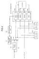
- Fig. 1 is a block diagram of a relevant structure of a chip according to an embodiment of the present invention.
- the chip shown in Fig. 1 includes an external bus controller 101, a move-in (hereinafter, "MI") data RAM 102, a bypass path 103, a selector 104, an input and output controller 105, a monitoring unit 106, CPU cores 107-1 and 107-2, L1 caches 107a-1 and 107a-2, a data register 108, a move-in buffer (hereinafter, "MIB”) 109, a write controller 110, and an L2 cache 111.
- MIB move-in buffer
- FIG. 1 depicts four inflow paths for MI data to the chip, the number of inflow paths for MI data may be one or a plural number other than four.
- the external bus controller 101 is connected to an upper-level cache, a main memory, or other chips (all not shown) provided outside of the chip through external buses.
- the external bus controller 101 controls a plurality of external buses (four in Fig. 1 ) that serve as paths through which data is flowed in the chip, and temporarily registers MI data flowing in from the external buses in an internal register thereof. Further, the external bus controller 101 inputs MI data from any of the external buses to the MI data RAM 102 and the bypass path 103, in synchronization with the control performed by the input and output controller 105.
- the MI data RAM 102 stores therein MI data output from the external bus controller 101.
- the MI data RAM 102 outputs MI data to the data register 108 via the selector 104.
- the MI data RAM 102 serves as a buffer provided upstream of the data register 108.
- the MI data RAM 102 is constituted by a static random access memory (SRAM) capable of storing therein all pieces of MI data that are transferred in response to all move-in requests issued in same time period.
- SRAM static random access memory
- the MI data RAM 102 is a buffer for the data register 108, there is no need to increase the amounts of inflow data and outflow data per unit time according to the amount of data to be written to the cache. However, a certain throughput needs to be achieved that can process the amount of inflow data from the external buses.
- the bypass path 103 allows bypassing of MI data output from the external bus controller 101. If the data register 108 has an area available for retrieving the MI data or if the bypass path 103 needs to output MI data directly to the CPU cores 107-1 and 107-2, the bypass path 103 outputs the MI data to the data register 108 or the CPU cores 107-1 and 107-2 via the selector 104.
- the selector 104 selectively outputs either MI data stored in the MI data RAM 102 or MI data passed through the bypass path 103 to the data register 108 and the CPU cores 107-1 and 107-2.
- the input and output controller 105 performs control such that MI data flowing in the external bus controller 101 in the cycle of the external buses is input to the MI data RAM 102 and the bypass path 103 in the CPU cycle, and that the selector 104 outputs the MI data supplied from the MI data RAM 102 or the bypass path 103.
- the input and output controller 105 selectively determines either the MI data RAM 102 or the bypass path 103 as a source of MI data depending on whether an available space is in the data register 108 based on a report from the monitoring unit 106, so as to control the selector 104 to output MI data from the determined source.
- the input and output controller 105 After causing the selector 104 to output the MI data, the input and output controller 105 notifies the MIB 109 of information about the MI data thus output. As to when the MI data is input or output under the control of the input and output controller 105, details will be described later.
- the monitoring unit 106 monitors whether an available space is in the data register 108. If the data register 108 has a size available for retrieving MI data, the monitoring unit 106 reports it to the input and output controller 105. As shown in Fig. 2 , the monitoring unit 106 monitors whether an available space is in a move-in data queue (hereinafter, "MIDQ") 108a in the data register 108, which will be described later in detail.
- MIDQ move-in data queue
- the size of the MID 108a may be equally divided according to the number of external buses so that the monitoring unit 106 may monitor available areas of the divided sizes corresponding to the external buses. In this way, when a plurality of external buses are connected to the chip, data pieces flowing in from the respective external buses can be equally retrieved in the MIDQ 108a.
- the CPU cores 107-1 and 107-2 incorporate the L1 caches 107a-1 and 107a-2, respectively, and perform predetermined processes using data stored in the L1 caches 107a-1 and 107a-2, data read from the L2 cache 111, and MI data supplied from the outside of the chip.
- the data register 108 once retrieves data to be written to the L2 cache 111 and data read from the L2 cache 111, writes write data including MI data to the L2 cache 111, and outputs the read out data to, for example, the L1 caches 107a-1 and 107a-2 of the CPU cores 107-1 and 107-2.
- the data register 108 includes the MIDQ 108a, a write-back data queue (hereinafter, "WBDQ”) 108b, a move-out data queue (hereinafter, "MODQ”) 108c, and a read data queue (hereinafter, "RDQ”) 108d, for example as shown in Fig. 2 .
- the MIDQ 108a retrieves MI data output from the selector 104, and writes the MI data thus retrieved to the L2 cache 111.
- the MIDQ 108a has a size allowing retrieval of two data sets for one external bus. In the present embodiment, because four external buses are connected to the chip, the MIDQ 108a has a size allowing retrieval of eight data sets in total. With this structure, data from all the external buses can be processed such that while a data piece is being retrieved in the MIDQ 108a, a data piece already stored in the MIDQ 108a is written to the L2 cache 111.
- the WBDQ 108b retrieves write-back data to be written back from the L1 caches 107a-1 and 107a-2, and writes to the L2 cache 111 the write-back data thus retrieved.
- the MODQ 108c reads from the L2 cache 111 move-out data ("MO data" in Fig. 2 ) that is externally requested outside of the chip to be moved out from the L2 cache 111, so as to output it to an external destination, outside of the chip, having made the move-out request.
- the RDQ 108d reads from the L2 cache 111 read data that is requested by the CPU cores 107-1 and 107-2 to be read out, so as to output it to the CPU cores 107-1 and 107-2.
- the MIB 109 is a buffer that stores therein requests for moving data into the L2 cache 111.
- the MIB 109 deletes a request that corresponds to the MI data, and notifies the write controller 110 of the deletion.
- the write controller 110 controls the data register 108 to write to the L2 cache 111 MI data that corresponds to the request thus deleted from the MIB 109. Specifically, when notified that the request has been deleted by the MIB 109, the write controller 110 instructs the data register 108 to write to the L2 cache 111 MI data that has been retrieved in the MIDQ 108a, and that corresponds to the deleted request.
- the L2 cache 111 stores therein data required by the CPU cores 107-1 and 107-2.
- desirable data is moved in from the upper-level cache, the main memory, or other chips outside of the chip.
- the external bus controller 101, the MI data RAM 102, the bypass path 103, the selector 104, the input and output controller 105, the monitoring unit 106, the data register 108, the MIB 109, and the write controller 110 control writing of MI data to the L2 cache 111, constituting a cache controller according to the present embodiment.
- MI data is flowed in the external bus controller 101 of the chip.
- pieces of MI data are flowed in the external bus controller 101 from respective external buses.
- the timing as to when the pieces of MI data are flowed in from the external buses may differ.
- the following describes an arrangement in which MI data is flowed in from any one of the external buses.
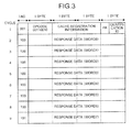
- MI data flowing in the external bus controller 101 is configured as a packet, for example, as shown in Fig. 3 .
- the header of four bytes is flowed in the external bus controller 101 in the first cycle of the external bus, and the body of the MI data, i.e., response data (WORD0 to WORD7), is flowed in the external bus controller 101 in the second to the ninth cycles of the external bus.
- the header of the packet of the MI data includes: an operation code (OPCODE) indicating that the packet is a data packet, not a command packet or the like; and a parity bit (PA) used for detecting errors in the packet.
- OPCODE operation code
- PA parity bit
- Data of four bytes flows in each cycle of the external bus.
- Each cycle begins with a tag added for indicating whether the cycle is a header or data.
- a cycle with a tag "001" is a header
- a cycles with a tag "100” is data
- a cycle with a tag "101” is an end of the data.
- Such a packet i.e., the MI data flowed in the external bus controller 101 from the external bus, is once registered in the register of the external bus controller 101, and then input from the external bus controller 101 to the MI data RAM 102 and the bypass path 103 under the control of the input and output controller 105.
- the input and output controller 105 causes the external bus controller 101 to output MI data at a speed that allows MI data flowing in from the external bus not to exceed the acceptable amount of data in the register in the external bus controller 101, so that the MI data is input to the MI data RAM 102 and the bypass path 103.
- the data passed through the bypass path 103 can be retransmitted from the MI data RAM 102.
- the data may be input to either the MI data RAM 102 or the bypass path 103 according to the selection made by the selector 104 as described below.
- the monitoring unit 106 constantly monitors whether an available space is in the MIDQ 108a of the data register 108. If an available area for retrieving MI data is found in the MIDQ 108a, it is reported to the input and output controller 105. Specifically, if an available area is found in the MIDQ 108a, the input and output controller 105 causes the selector 104 to output MI data from the MI data RAM 102 or the bypass path 103 to the MIDQ 108a.
- the input and output controller 105 causes the selector 104 to output MI data supplied, from the bypass path 103.
- the input and output controller 105 causes the selector 104 to output the MI data supplied from the MI data RAM 102.
- MI data is selectively output from the selector 104. This allows MI data to be output to the MIDQ 108a in order of the MI data flowed in the chip from the external bus. Further, if no MI data has been stored in the MI data RAM 102, MI data is output to the MID 108a directly from the bypass path 103. This enables to reduce the time for writing MI data to the MI data RAM 102.
- the input and output controller 105 may control the selector 104 to output MI data supplied from the bypass path 103 directly to the CPU cores 107-1 and 107-2.
- the input and output controller 105 controls the selector 104 and the MI data is output to the MIDQ 108a
- information about the MI data is reported to the MIB 109.
- the MIB 109 deletes the move-in request that corresponds to the MI data thus notified by the input and output controller 105, and the deletion is notified to the write controller 110.
- the write controller 110 provides, aiming to complete the move-in of the corresponding MI data, the MIDQ 108a of the data register 108 with an instruction for writing to the L2 cache 111 the MI data that corresponds to the request deleted from the MIB 109.
- the MIDQ 108a writes the MI data to the L2 cache 111, and the move-in is complete.
- the MIDQ 108a Upon completion of the move-in, the MIDQ 108a has an available area. Thus, the monitoring unit 106 reports the available area to the input and output controller 105, causing again the selector 104 to output MI data supplied either from the MI data RAM 102 or the bypass path 103.
- the following describes the timing as to when MI data is input to and output from the MI data RAM 102 under the control of the input and output controller 105. Assume that the CPU cycle is three times as fast as the cycle of the external bus and the transferable volume in the internal bus is twice as much as the transferable volume in the external bus. Further, as MI data, the packet shown in Fig. 3 is flowed in the external bus controller 101.
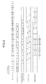
- the MI data is received by the chip every cycle of the external bus (three CPU cycles) in the order of the header, data W0, data W1, ..., and data W7.
- data of four bytes is received every three CPU cycles, and the data thus received is flowed in the external bus controller 101 and retained in a register #1 in the external bus controller 101.
- the data thus received in units of four bytes is bundled into data of eight bytes including the data W0 to the data W7, and retained in a register #2. Because the register #2 retains the data in units of eight bytes, the data W0 to the data W7 of four bytes each are retained for a time required for receiving data of eight bytes, i.e., six CPU cycles.
- MI data flows in the external bus controller 101 from four inflow paths, i.e., the external buses #1 to #4.
- MI data flows in from any of the external buses #1 and #4 in a similar manner as described above, and therefore data from all the four external buses needs to be input to the MI data RAM 102 and the bypass path 103 during the six CPU cycles.
- data from each of the external buses may be input to the MI data RAM 102 and the bypass path 103 during the assigned cycle.
- the data from the four external buses #1 to #4 is input to the MI data RAM 102 and the bypass path 103 during four CPU cycles, thus preventing data overflow in the register of the external bus controller 101.
- the amount of data to be input to the MI data RAM 102 in one cycle differs depending on the number of external buses, the clock rate of the chip, the difference in transferable volume between the external bus and the internal bus, and other factors. Therefore, the MI data RAM 102 needs to be capable of accepting the amount of data input in one cycle. Because this amount of data is significantly less than the amount of data accepted in one cycle at the MIDQ 108a of the data register 108, a control circuit and a data bus used for the MI data RAM 102 are dimensionally negligible compared with those used for a RAM serving as a substitute for the data register.
- the MI data RAM 102 can perform only either reading or writing of data during one cycle in general. Thus, when four cycles out of six cycles are used for inputting data from the external buses #1 to #4, one cycle of the remaining two cycles is used for outputting data.
- the other remaining cycle is desirably set as an idle cycle for an interval between data input and data output, thereby preventing interference between input data and output data.
- the data from the four external buses #1 to #4 is input to and output from the MI data RAM 102 so that no data overflows from the MI data RAM 102.
- This enables retrieval of more data to be written to the L2 cache 111, compared with a chip including only the data register 108.
- the MI data RAM 102 is connected to the MIDQ 108a of the data register 108, not directly to the L2 cache 111, so that a two-stage buffer is constituted.
- the amounts of inflow data and outflow data per unit time at the MI data RAM 102 may be significantly less than those at the MIDQ 108a, thus achieving downsizing and cost reduction of a control circuit and a data bus used for the MI data RAM 102.
- the distance between the RAM and the MIDQ 108a is not spatially limited, and the position of the MI data RAM 102 is flexibly determined on the chip. Accordingly, circuit placement on the chip can be flexibly determined. Further, because the data register 108 does not change in size, for example, as shown in Fig. 6 , dead zones serving no function on the chip (area indicated by hatched lines in Fig. 6 ) can be suppressed to the minimum.
- MIDR indicates the position of the MI data RAM 102
- CONTROL BLOCK indicates the position of the processing blocks such as the input and output controller 105, the monitoring unit 106, the MIB 109, and the write controller 110.
- the RAM that stores therein MI data is provided upstream of the data register in the chip, so as to store therein MI data flowing in the chip. This enables retrieval of large amounts of MI data to be written to the cache memory. Further, because the RAM itself does not perform write operation to the cache memory, an increase in circuit size and cost due to the provision of the RAM is minimized.
- data is written to the L2 cache 111 in the order that the data is output from the MI data RAM 102 to the MIDQ 108a.
- a wait may be required to write data from the MIDQ 108a to the L2 cache 111.
- Such a state may be found by the MIB 109 based on the notification made by the input and output controller 105 and the request being stored.
- data once retrieved in the MIDQ 108a may be discarded to retrieve subsequent data from the MI data RAM 102 for write operation. Further, the data thus discarded may be retrieved in the MIDQ 108a again for write operation.
- the present invention is applicable to retrieval of large amounts of data to be written to a cache memory, achieving downsizing and cost reduction of a chip.
Landscapes
- Engineering & Computer Science (AREA)
- Theoretical Computer Science (AREA)
- Physics & Mathematics (AREA)
- General Engineering & Computer Science (AREA)
- General Physics & Mathematics (AREA)
- Memory System Of A Hierarchy Structure (AREA)
Abstract
Description
- The present invention relates to a cache controller and a cache control method for writing data to a cache memory. The invention particularly relates to a cache controller and a cache control method that enable retrieval of large amounts of data to be written to a cache memory, while achieving downsizing and cost reduction of a chip.
- Recently, most information processing apparatuses such as computers include a central processing unit (CPU) incorporating a cache memory to improve the processing speed of the CPU by reducing the number of accesses to a main memory generally having low access speed. A cache memory is accessible at high speed. However, because the cache memory has a smaller size than that of the main memory, the cache memory does not always store therein data required by the CPU (i.e., cache miss). In such a case, data stored in an upper-level cache such as a secondary cache or in the main memory needs to be moved in the cache memory on the CPU.
- In general, data to be moved in the cache memory is temporarily retrieved in a data register connected to the cache memory, and then written to the cache memory from the data register.
- Recent years have seen remarkable technological developments that increase the processing speed of CPUs and also the size of main memories. As a result, a CPU requires more data per unit time, while taking a longer time to retrieve the data from the main memory. This causes a speed discrepancy between the CPU and the main memory, thus relatively increasing memory latency.
- Under such circumstances, proper control for moving data into a cache memory is important. For example,
Patent Document 1 discloses a technology that reduces the amount of data to be moved-in when a main memory has increased loads, and that resumes a move-in of data having an equivalent amount to the reduced data when the load of the main memory becomes smaller. - The technology disclosed in
Patent Document 1 can efficiently adjust the data move-in when a cache miss occurs. However, the CPU using the data to be moved-in runs at a processing speed limited by the speed of the main memory, thus the technology cannot offset the increased memory latency completely. In this case, the CPU may execute subsequent processes one after another, while performing the move-in of the data for handling the cache miss to improve throughput. This may cause more cache misses simultaneously, increasing the amount of data to be moved-in. Thus, there is a demand to increase the amount of data retrievable at one time by a data register that writes data to the cache memory. - Patent Document 1: Japanese Patent Application Laid-open No.
H7-210460 - When a data queue in the data register is simply expanded to increase the size of the data register, the data queue dimensionally exceeds a current chip. This is unrealistic because such a chip on which a CPU is mounted needs to have a larger size opposing the downsizing of the chip.
- Alternatively, a low cost random access memory (RAM) may be used as a substitute for the data register. Because the data register holds data to be written to the cache memory only temporarily, the RAM serving as a substitute for the data register only needs to have a significantly small size compared with the cache memory.
To improve throughput with the RAM having such a small size and serving as a substitute for the data register, the amounts of inflow data and outflow data to and from the RAM per unit time need to be increased according to the amount of data to be written to the cache memory. As a result, a control circuit and a data bus used for the RAM occupy a large area, causing an increase in space and cost of the portion substituting for the data register. - The present invention is made in view of the above problems, and an object of the present invention is to provide a cache controller and a cache control method that enable retrieval of large amounts of data to be written to a cache memory, while achieving downsizing and cost reduction of a chip.
- To solve the problems as described above, a cache controller according to the present invention writes data to a cache memory, and includes a first buffer unit that retains data flowing in from outside to be written to the cache memory, a second buffer unit that retains a data piece to be currently written to the cache memory, among pieces of the data a retained in the first buffer unit, and a write controlling unit that controls writing of the data piece retained in the second buffer unit to the cache memory.
- Further, in the cache controller according to the present invention, in an aspect of the present invention as described above, the first buffer unit includes a RAM capable of storing therein all data pieces that can be simultaneously requested to be written to the cache memory.
- Further, the cache controller according to the present invention, in an aspect of the present invention as described above, further includes a monitoring unit that monitors whether the second buffer unit has an available area, and when the monitoring unit finds an available area in the second buffer unit, the first buffer unit outputs data to the second buffer unit.
- Further, in the cache controller according to the present invention, in an aspect of the present invention as described above, the second buffer unit is disposed near the cache memory, and the first buffer unit is disposed farther away from the cache memory than the second buffer unit.
- Further, in the cache controller according to the present invention, in an aspect of the present invention as described above, the first buffer unit includes an external bus controlling unit that controls data flowing in from a plurality of external buses, and the second buffer unit includes areas that correspond to the external buses, and that retain equal amounts of data.
- Further, in the cache controller according to the present invention, in an aspect of the present invention as described above, the second buffer unit includes an area for retaining two sets of write data for each of the external buses.
- Further, the cache controller according to the present invention, in an aspect of the present invention as described above, further includes a bypass unit that allows data flowing in from outside to bypass the first buffer unit, and a selecting unit that selectively outputs either data output from the first buffer unit or data output from the bypass unit to the second buffer unit.
- Further, in the cache controller according to the present invention in an aspect of the present invention as described above, the selecting unit selects the data output from the bypass unit when the second buffer unit has an available area.
- Further, in the cache controller according to the present invention, in an aspect of the present invention as described above, when the first buffer unit outputs data to the second buffer unit, the write controlling unit controls the second buffer unit to write the data to the cache memory.
- Further, a cache control method of writing data to a cache memory, according to another aspect of the present invention includes a first storing step of storing in a first buffer, data flowing in from outside to be written to the cache memory, a second storing step of storing in a second buffer, a data piece to be currently written to the cache memory, among pieces of the data stored in the first storing step and a write controlling step of controlling writing of the data piece stored in the second storing step to the cache memory.
- According to the present invention, data flowing in from the outside to be written to the cache memory is retained in the first buffer, a data piece to be currently written to the cache memory is retained in the second buffer, so that the data piece retained in the second buffer is controlled to be written to the cache memory. Thus, by using a normal data register as the second buffer, the first buffer can employ a RAM that has small amounts of inflow data and outflow data per unit time, and that incorporates a small size circuit. This enables retrieval of large amounts of data to be written to the cache memory, while achieving downsizing and cost reduction of a chip.
- According to the present invention, the first buffer includes a RAM of a size capable of storing therein all data pieces that can be simultaneously requested to be written to the cache memory. This enables storage of, for example, data pieces of responses corresponding to all move-in requests issued when a cache miss occurs and allows the CPU to perform the subsequent processes, thereby increasing throughput.
- According to the present invention, whether an available area is in the second buffer is monitored, and if an available area is found in the second buffer, the first buffer outputs data to the second buffer. This prevents data overflow in the second buffer that retains data to be written directly to the cache memory, thereby reliably writing all the data to the cache memory.
- According to the present invention, the second buffer is disposed near the cache memory, and the first buffer is disposed farther away from the cache memory than the second buffer. Thus, data can be written quickly from the second buffer to the cache memory, and the position of the first buffer can be flexibly determined on the chip.
- According to the present invention, the first buffer controls data flowing in from a plurality of external buses, and the second buffer includes areas that correspond to the external buses, and that respectively retain data pieces of equal amounts. Thus, even when data is flowed in the first buffer through the external buses from the outside of the chip, data pieces from the respective external buses can be equally written to the cache memory.
- According to the present invention, the second buffer includes an area that retains two sets of write data for each of the external buses. Therefore, while the first set of write data is being written to the cache memory, the next set of write data can be retrieved from the first buffer, thus data can be efficiently written to the cache memory.
- According to the present invention, data flowing in from the outside is allowed to bypass the first buffer, and either data output from the first buffer or data that has bypassed the first buffer is selectively output to the second buffer. This enables the second buffer to directly retrieve data as necessary, thus shortening the time required for input and output of data to and from the first buffer.
- According to the present invention, when the second buffer has an available area, the data that has bypassed the first buffer is selected. This shortens the time for data to be written to the cache memory after its flowing in the chip, when the second buffer has an available area and the time required for input and output of data to and from the first buffer will be wasted.
- According to the present invention, when data is output from the first buffer to the second buffer, the second buffer writes the data to the cache memory. Because the data to be written to the cache memory has been retrieved in the second buffer at write operation, performed to the cache memory, the data flowed in the chip can be reliably written to the cache memory.
-
- [
Fig. 1] Fig. 1 is a block diagram of a relevant structure of a chip according to an embodiment of the present invention. - [
Fig. 2] Fig. 2 is a block diagram of an internal structure of a data register according to the embodiment. - [
Fig. 3] Fig. 3 depicts an exemplary packet configuration of move-in data according to the embodiment. - [
Fig. 4] Fig. 4 depicts how data flows in the chip according to the embodiment. - [
Fig. 5A] Fig. 5A depicts an example regarding the timing of input and output of data moved in a RAM according to the embodiment. - [
Fig. 5B] Fig. 5B depicts another example regarding the timing of input and output of data moved in the RAM according to the embodiment. - [
Fig. 6] Fig. 6 is a diagram of exemplary circuit placement on the chip according to the embodiment. -
- 101
- External bus controller
- 102
- MI data RAM
- 103
- Bypass path
- 104
- Selector
- 105
- Input and output controller
- 106
- Monitoring unit
- 107-1, 107-2
- CPU core
- 107a-1, 107a-2
- L1 cache
- 108
- Data register
- 108a
- MIDQ
- 108b
- WBDQ
- 108c
- MCDQ
- 108d
- RDQ
- 109
- MIB
- 110
- Write controller
- 111
- L2 cache
- An embodiment of the present invention will now be described in detail with reference to the accompanying drawings. The following describes a chip incorporating: two CPU cores each including a
level 1 cache (L1 cache); and alevel 2 cache (L2 cache), in which data is moved in the L2 cache. The present invention can be similarly applied to an arrangement in which data is written to other caches. -
Fig. 1 is a block diagram of a relevant structure of a chip according to an embodiment of the present invention. The chip shown inFig. 1 includes anexternal bus controller 101, a move-in (hereinafter, "MI")data RAM 102, abypass path 103, aselector 104, an input andoutput controller 105, amonitoring unit 106, CPU cores 107-1 and 107-2,L1 caches 107a-1 and 107a-2, adata register 108, a move-in buffer (hereinafter, "MIB") 109, awrite controller 110, and anL2 cache 111. AlthoughFig. 1 depicts four inflow paths for MI data to the chip, the number of inflow paths for MI data may be one or a plural number other than four. - The
external bus controller 101 is connected to an upper-level cache, a main memory, or other chips (all not shown) provided outside of the chip through external buses. Theexternal bus controller 101 controls a plurality of external buses (four inFig. 1 ) that serve as paths through which data is flowed in the chip, and temporarily registers MI data flowing in from the external buses in an internal register thereof. Further, theexternal bus controller 101 inputs MI data from any of the external buses to theMI data RAM 102 and thebypass path 103, in synchronization with the control performed by the input andoutput controller 105. - The MI data RAM 102 stores therein MI data output from the
external bus controller 101. When the data register 108 has a space available for retrieving MI data, theMI data RAM 102 outputs MI data to the data register 108 via theselector 104. Thus, theMI data RAM 102 serves as a buffer provided upstream of the data register 108. Specifically, theMI data RAM 102 is constituted by a static random access memory (SRAM) capable of storing therein all pieces of MI data that are transferred in response to all move-in requests issued in same time period. - Because the
MI data RAM 102 is a buffer for the data register 108, there is no need to increase the amounts of inflow data and outflow data per unit time according to the amount of data to be written to the cache. However, a certain throughput needs to be achieved that can process the amount of inflow data from the external buses. - The
bypass path 103 allows bypassing of MI data output from theexternal bus controller 101. If thedata register 108 has an area available for retrieving the MI data or if thebypass path 103 needs to output MI data directly to the CPU cores 107-1 and 107-2, thebypass path 103 outputs the MI data to the data register 108 or the CPU cores 107-1 and 107-2 via theselector 104. - According to the control performed by the input and
output controller 105, theselector 104 selectively outputs either MI data stored in theMI data RAM 102 or MI data passed through thebypass path 103 to the data register 108 and the CPU cores 107-1 and 107-2. - The input and
output controller 105 performs control such that MI data flowing in theexternal bus controller 101 in the cycle of the external buses is input to theMI data RAM 102 and thebypass path 103 in the CPU cycle, and that theselector 104 outputs the MI data supplied from theMI data RAM 102 or thebypass path 103. To this end, the input andoutput controller 105 selectively determines either theMI data RAM 102 or thebypass path 103 as a source of MI data depending on whether an available space is in the data register 108 based on a report from themonitoring unit 106, so as to control theselector 104 to output MI data from the determined source. - After causing the
selector 104 to output the MI data, the input andoutput controller 105 notifies theMIB 109 of information about the MI data thus output. As to when the MI data is input or output under the control of the input andoutput controller 105, details will be described later. - The
monitoring unit 106 monitors whether an available space is in the data register 108. If thedata register 108 has a size available for retrieving MI data, themonitoring unit 106 reports it to the input andoutput controller 105. As shown inFig. 2 , themonitoring unit 106 monitors whether an available space is in a move-in data queue (hereinafter, "MIDQ") 108a in the data register 108, which will be described later in detail. In this arrangement, the size of theMID 108a may be equally divided according to the number of external buses so that themonitoring unit 106 may monitor available areas of the divided sizes corresponding to the external buses. In this way, when a plurality of external buses are connected to the chip, data pieces flowing in from the respective external buses can be equally retrieved in theMIDQ 108a. - The CPU cores 107-1 and 107-2 incorporate the
L1 caches 107a-1 and 107a-2, respectively, and perform predetermined processes using data stored in theL1 caches 107a-1 and 107a-2, data read from theL2 cache 111, and MI data supplied from the outside of the chip. - The data register 108 once retrieves data to be written to the
L2 cache 111 and data read from theL2 cache 111, writes write data including MI data to theL2 cache 111, and outputs the read out data to, for example, theL1 caches 107a-1 and 107a-2 of the CPU cores 107-1 and 107-2. Specifically, the data register 108 includes theMIDQ 108a, a write-back data queue (hereinafter, "WBDQ") 108b, a move-out data queue (hereinafter, "MODQ") 108c, and a read data queue (hereinafter, "RDQ") 108d, for example as shown inFig. 2 . - The
MIDQ 108a retrieves MI data output from theselector 104, and writes the MI data thus retrieved to theL2 cache 111. TheMIDQ 108a has a size allowing retrieval of two data sets for one external bus. In the present embodiment, because four external buses are connected to the chip, theMIDQ 108a has a size allowing retrieval of eight data sets in total. With this structure, data from all the external buses can be processed such that while a data piece is being retrieved in theMIDQ 108a, a data piece already stored in theMIDQ 108a is written to theL2 cache 111. - The
WBDQ 108b retrieves write-back data to be written back from theL1 caches 107a-1 and 107a-2, and writes to theL2 cache 111 the write-back data thus retrieved. TheMODQ 108c reads from theL2 cache 111 move-out data ("MO data" inFig. 2 ) that is externally requested outside of the chip to be moved out from theL2 cache 111, so as to output it to an external destination, outside of the chip, having made the move-out request. TheRDQ 108d reads from theL2 cache 111 read data that is requested by the CPU cores 107-1 and 107-2 to be read out, so as to output it to the CPU cores 107-1 and 107-2. - Referring back to
Fig. 1 , theMIB 109 is a buffer that stores therein requests for moving data into theL2 cache 111. When notified of information about the MI data by the input andoutput controller 105, theMIB 109 deletes a request that corresponds to the MI data, and notifies thewrite controller 110 of the deletion. - The
write controller 110 controls the data register 108 to write to theL2 cache 111 MI data that corresponds to the request thus deleted from theMIB 109. Specifically, when notified that the request has been deleted by theMIB 109, thewrite controller 110 instructs the data register 108 to write to theL2 cache 111 MI data that has been retrieved in theMIDQ 108a, and that corresponds to the deleted request. - The
L2 cache 111 stores therein data required by the CPU cores 107-1 and 107-2. When theL2 cache 111 stores therein no data required by the CPU cores 107-1 and 107-2 (when a cache miss occurs), desirable data is moved in from the upper-level cache, the main memory, or other chips outside of the chip. - Among these processing blocks, the
external bus controller 101, theMI data RAM 102, thebypass path 103, theselector 104, the input andoutput controller 105, themonitoring unit 106, thedata register 108, theMIB 109, and thewrite controller 110 control writing of MI data to theL2 cache 111, constituting a cache controller according to the present embodiment. - The following describes operations for moving data into the
cache 111 on the chip having the above structure. - When the CPU cores 107-1 and 107-2 request reading of data from the
L2 cache 111 and a cache miss occurs because no desirable data is stored in theL2 cache 111, a request is made to the upper-level cache, the main memory, or other chips outside of the chip to perform a data move-in therefrom. Such a request issued in response to a move-in request is stored in theMIB 109. - In response to the move-in request, MI data is flowed in the
external bus controller 101 of the chip. InFig. 1 , pieces of MI data are flowed in theexternal bus controller 101 from respective external buses. The timing as to when the pieces of MI data are flowed in from the external buses may differ. The following describes an arrangement in which MI data is flowed in from any one of the external buses. - MI data flowing in the
external bus controller 101 is configured as a packet, for example, as shown inFig. 3 . Specifically, the header of four bytes is flowed in theexternal bus controller 101 in the first cycle of the external bus, and the body of the MI data, i.e., response data (WORD0 to WORD7), is flowed in theexternal bus controller 101 in the second to the ninth cycles of the external bus. As shown inFig. 3 , the header of the packet of the MI data includes: an operation code (OPCODE) indicating that the packet is a data packet, not a command packet or the like; and a parity bit (PA) used for detecting errors in the packet. - Data of four bytes (i.e., 32 bits) flows in each cycle of the external bus. Each cycle begins with a tag added for indicating whether the cycle is a header or data. Specifically, for example, in
Fig. 3 , a cycle with a tag "001" is a header, a cycles with a tag "100" is data, and a cycle with a tag "101" is an end of the data. - Such a packet, i.e., the MI data flowed in the
external bus controller 101 from the external bus, is once registered in the register of theexternal bus controller 101, and then input from theexternal bus controller 101 to theMI data RAM 102 and thebypass path 103 under the control of the input andoutput controller 105. To this end, considering differences between the cycle of the external bus and the CPU cycle, differences in transferable volume between the external bus and an internal bus in the chip, and other factors, the input andoutput controller 105 causes theexternal bus controller 101 to output MI data at a speed that allows MI data flowing in from the external bus not to exceed the acceptable amount of data in the register in theexternal bus controller 101, so that the MI data is input to theMI data RAM 102 and thebypass path 103. In the present embodiment, because MI data is input to both theMI data RAM 102 and thebypass path 103, the data passed through thebypass path 103 can be retransmitted from theMI data RAM 102. However, when there is no need to retransmit the data, the data may be input to either theMI data RAM 102 or thebypass path 103 according to the selection made by theselector 104 as described below. - On the other hand, the
monitoring unit 106 constantly monitors whether an available space is in theMIDQ 108a of the data register 108. If an available area for retrieving MI data is found in theMIDQ 108a, it is reported to the input andoutput controller 105. Specifically, if an available area is found in theMIDQ 108a, the input andoutput controller 105 causes theselector 104 to output MI data from theMI data RAM 102 or thebypass path 103 to theMIDQ 108a. - If the
MIDQ 108a has an available area when the MI data is output from theexternal bus controller 101, and also if the MI data RAM 102 stores therein no MI data, the input andoutput controller 105 causes theselector 104 to output MI data supplied, from thebypass path 103. On the contrary, if theMI data RAM 102 has already stored therein MI data, the input andoutput controller 105 causes theselector 104 to output the MI data supplied from theMI data RAM 102. - Accordingly, MI data is selectively output from the
selector 104. This allows MI data to be output to theMIDQ 108a in order of the MI data flowed in the chip from the external bus. Further, if no MI data has been stored in theMI data RAM 102, MI data is output to theMID 108a directly from thebypass path 103. This enables to reduce the time for writing MI data to theMI data RAM 102. - When the CPU cores 107-1 and 107-2 directly request MI data, for example, for prefetching, the input and
output controller 105 may control theselector 104 to output MI data supplied from thebypass path 103 directly to the CPU cores 107-1 and 107-2. - When the input and
output controller 105 controls theselector 104 and the MI data is output to theMIDQ 108a, information about the MI data is reported to theMIB 109. Then, theMIB 109 deletes the move-in request that corresponds to the MI data thus notified by the input andoutput controller 105, and the deletion is notified to thewrite controller 110. Upon deletion of the move-in request from theMIB 109, thewrite controller 110 provides, aiming to complete the move-in of the corresponding MI data, theMIDQ 108a of the data register 108 with an instruction for writing to theL2 cache 111 the MI data that corresponds to the request deleted from theMIB 109. In response to the instruction, theMIDQ 108a writes the MI data to theL2 cache 111, and the move-in is complete. - Upon completion of the move-in, the
MIDQ 108a has an available area. Thus, themonitoring unit 106 reports the available area to the input andoutput controller 105, causing again theselector 104 to output MI data supplied either from theMI data RAM 102 or thebypass path 103. - Referring to a specific example, the following describes the timing as to when MI data is input to and output from the
MI data RAM 102 under the control of the input andoutput controller 105. Assume that the CPU cycle is three times as fast as the cycle of the external bus and the transferable volume in the internal bus is twice as much as the transferable volume in the external bus. Further, as MI data, the packet shown inFig. 3 is flowed in theexternal bus controller 101. - As shown in
Fig. 4 , the MI data is received by the chip every cycle of the external bus (three CPU cycles) in the order of the header, data W0, data W1, ..., and data W7. Specifically, data of four bytes is received every three CPU cycles, and the data thus received is flowed in theexternal bus controller 101 and retained in aregister # 1 in theexternal bus controller 101. Depending on the transferable volume in the internal bus, the data thus received in units of four bytes is bundled into data of eight bytes including the data W0 to the data W7, and retained in aregister # 2. Because theregister # 2 retains the data in units of eight bytes, the data W0 to the data W7 of four bytes each are retained for a time required for receiving data of eight bytes, i.e., six CPU cycles. - The foregoing describes data flowing in from one external bus. In the present embodiment, MI data flows in the
external bus controller 101 from four inflow paths, i.e., theexternal buses # 1 to #4. MI data flows in from any of theexternal buses # 1 and #4 in a similar manner as described above, and therefore data from all the four external buses needs to be input to theMI data RAM 102 and thebypass path 103 during the six CPU cycles. To this end, by assigning one CPU cycle to each of theexternal buses # 1 to #4, data from each of the external buses may be input to theMI data RAM 102 and thebypass path 103 during the assigned cycle. In this way, the data from the fourexternal buses # 1 to #4 is input to theMI data RAM 102 and thebypass path 103 during four CPU cycles, thus preventing data overflow in the register of theexternal bus controller 101. - Accordingly, the amount of data to be input to the
MI data RAM 102 in one cycle differs depending on the number of external buses, the clock rate of the chip, the difference in transferable volume between the external bus and the internal bus, and other factors. Therefore, theMI data RAM 102 needs to be capable of accepting the amount of data input in one cycle. Because this amount of data is significantly less than the amount of data accepted in one cycle at theMIDQ 108a of the data register 108, a control circuit and a data bus used for theMI data RAM 102 are dimensionally negligible compared with those used for a RAM serving as a substitute for the data register. - The
MI data RAM 102 can perform only either reading or writing of data during one cycle in general. Thus, when four cycles out of six cycles are used for inputting data from theexternal buses # 1 to #4, one cycle of the remaining two cycles is used for outputting data. The other remaining cycle is desirably set as an idle cycle for an interval between data input and data output, thereby preventing interference between input data and output data. - Accordingly, in the chip connected to the four external buses, i.e., the
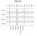
external buses # 1 to #4, when the throughput of the chip according to the transferable volume in the internal bus or the CPU clock rate is at least six times as high as the external buses, data from all theexternal buses # 1 to #4 is input to theMI data RAM 102 and output from theMT data RAM 102 during six cycles, as shown inFig. 5A . The data is not necessarily flowed in at the same timing from all theexternal buses # 1 to #4. However, for example, even when data from theexternal buses # 1 and #4 is flowed in with delay, the timing when the data from all theexternal buses # 1 to #4 is input to and output from theMI data RAM 102 is always in six cycles, as shown inFig. 5B . - The data from the four
external buses # 1 to #4 is input to and output from theMI data RAM 102 so that no data overflows from theMI data RAM 102. This enables retrieval of more data to be written to theL2 cache 111, compared with a chip including only the data register 108. Further, theMI data RAM 102 is connected to theMIDQ 108a of the data register 108, not directly to theL2 cache 111, so that a two-stage buffer is constituted. With this structure, the amounts of inflow data and outflow data per unit time at theMI data RAM 102 may be significantly less than those at theMIDQ 108a, thus achieving downsizing and cost reduction of a control circuit and a data bus used for theMI data RAM 102. - Further, by constituting the two-stage buffer in which the RAM is connected to the
MIDQ 108a, the distance between the RAM and theMIDQ 108a is not spatially limited, and the position of theMI data RAM 102 is flexibly determined on the chip. Accordingly, circuit placement on the chip can be flexibly determined. Further, because the data register 108 does not change in size, for example, as shown inFig. 6 , dead zones serving no function on the chip (area indicated by hatched lines inFig. 6 ) can be suppressed to the minimum. InFig. 6 , MIDR indicates the position of theMI data RAM 102, and CONTROL BLOCK indicates the position of the processing blocks such as the input andoutput controller 105, themonitoring unit 106, theMIB 109, and thewrite controller 110. - As described, according to the present embodiment, the RAM that stores therein MI data is provided upstream of the data register in the chip, so as to store therein MI data flowing in the chip. This enables retrieval of large amounts of MI data to be written to the cache memory. Further, because the RAM itself does not perform write operation to the cache memory, an increase in circuit size and cost due to the provision of the RAM is minimized.
- In the embodiment, data is written to the
L2 cache 111 in the order that the data is output from theMI data RAM 102 to theMIDQ 108a. For example, when data written to theL2 cache 111 needs to be replaced, a wait may be required to write data from theMIDQ 108a to theL2 cache 111. Such a state may be found by theMIB 109 based on the notification made by the input andoutput controller 105 and the request being stored. Thus, when a wait is required to write data retrieved in theMIDQ 108a, data once retrieved in theMIDQ 108a may be discarded to retrieve subsequent data from theMI data RAM 102 for write operation. Further, the data thus discarded may be retrieved in theMIDQ 108a again for write operation. - The present invention is applicable to retrieval of large amounts of data to be written to a cache memory, achieving downsizing and cost reduction of a chip.
- Embodiments of the present invention may also extend to the following statements:
-
Statement 1. A cache controller that writes data to a cache memory, (111) comprising:- a first buffer unit (102) that retains data, flowing in from outside to be written to the cache memory (111);
- a second buffer unit (108) that retains a data piece to be currently written to the cache memory (111), among pieces of the data retained in the first buffer unit (102);
and - a write controlling unit (110) that controls writing of the data piece retained in the second buffer unit (108) to the cache memory (111).
-
Statement 2. The cache controller according tostatement 1, wherein the first buffer unit (102) includes a random access memory (RAM) capable of storing therein all data pieces that can be simultaneously requested to be written to the cache memory (111). -
Statement 3. The cache controller according tostatement 1, further comprising a monitoring unit (106) that monitors whether the second buffer unit (108) has an available area,
wherein
when the monitoring unit (106) finds an available area in the second buffer unit (108), the first buffer unit (102) outputs data to the second buffer unit (108). -
Statement 4. The cache controller according tostatement 1, wherein
the second buffer unit (108) is disposed near the cache memory (111), and
the first buffer unit (102) is disposed farther away from the cache memory (111) than the second buffer unit (108). -
Statement 5. The cache controller according tostatement 1, wherein
the first buffer unit (102) includes an external bus controlling unit (101) that controls data flowing in from a plurality of external buses, and
the second buffer unit (108) includes areas that correspond to the external buses, and that retain equal amounts of data. -
Statement 6. The cache controller according tostatement 5, wherein the second buffer unit (108) includes an area for retaining two sets of write data for each of the external buses. -
Statement 7. The cache controller according tostatement 1, further comprising:- a bypass unit (103) that allows data flowing in from outside to bypass the first buffer unit (102); and
- a selecting unit (104) that selectively outputs either data output from the first buffer unit (102) or data output from the bypass unit (103) to the second buffer unit (108).
-
Statement 8. The cache controller according tostatement 7, wherein the selecting unit (104) selects the data output from the bypass unit (103) when the second buffer unit (108) has an available area. -
Statement 9. The cache controller according tostatement 1, wherein, when the first buffer unit (102) outputs data to the second buffer unit (108), the write controlling unit (110) controls the second buffer unit (108) to write the data to the cache memory (111). - Statement 10. A cache control method of writing data to a cache memory (111), comprising:
- a first storing step of storing in a first buffer unit (102), data flowing in from outside to be written to the cache memory (111);
- a second storing step of storing in a second buffer unit (108), a data piece to be currently written to the cache memory (111), among pieces of the data stored in the first storing step; and
- a write controlling step of controlling writing of the data piece stored in the second storing step to the cache memory (111).
Claims (8)
- A cache controller that writes data to a cache memory, (111) comprising:a first buffer unit (102) that retains data flowing in from outside to be written to the cache memory (111);a second buffer unit (108) that has a plurality of divided areas, each of the divided areas respectively retaining a data piece to be currently written to the cache memory (111), among pieces of the data retained in the first buffer unit (102);a monitoring unit (106) that monitors the divided areas of the second buffer unit (108) and reports whether the second buffer unit (108) has an available divided area; andan input and output controller (105) that controls the first buffer unit (102) to output the data piece to be currently written to the cache memory (111) to the second buffer unit (108) when it is reported by the monitoring unit (106) that the second buffer unit (108) has an available divided area.
- The cache controller according to claim 1, wherein the first buffer unit (102) includes a random access memory (RAM) capable of storing therein all data pieces that can be simultaneously requested to be written to the cache memory (111).
- The cache controller according to claim 1, wherein
the second buffer unit (108) is disposed near the cache memory (111), and
the first buffer unit (102) is disposed farther away from the cache memory (111) than the second buffer unit (108). - The cache controller according to claim 1, wherein
the first buffer unit (102) includes an external bus controlling unit (101) that controls data flowing in from a plurality of external buses, and
each of the divided areas of the second buffer unit (108) connects to a corresponding external bus among the plurality of external buses, and retains equal amounts of data, respectively. - The cache controller according to claim 1, further comprising:a bypass unit (103) that allows data flowing in from outside to bypass the first buffer unit (102); anda selecting unit (104) that selectively outputs either data output from the first buffer unit (102) or data output from the bypass unit (103) to the second buffer unit (108) according to control performed by the input and output controller (105).
- The cache controller according to claim 5, wherein the selecting unit (104) selects the data output from the bypass unit (103) when the second buffer unit (108) has an available divided area.
- The cache controller according to claim 1, further comprising a write controlling unit (110) that controls the divided areas of the second buffer unit (108) to write the data to the cache memory (111).
- A cache control method of writing data to a cache memory (111), comprising:storing in a first buffer unit (102), data flowing in from outside to be written to the cache memory (111);monitoring a second buffer unit (108) that has a plurality of divided areas, and reporting to an input and output controller (105) when the second buffer unit (108) has an available divided area;storing in the second buffer unit (108) a data piece to be currently written to the cache memory (111), among pieces of the data stored in the first buffer unit (102); andoutputting the data piece to be currently written in the cache memory (111) from the first buffer unit (102) to the second buffer unit (108) when it is reported that the second buffer unit (108) has an available divided area.
Priority Applications (1)
| Application Number | Priority Date | Filing Date | Title |
|---|---|---|---|
| EP10174845.7A EP2261804B1 (en) | 2006-02-27 | 2006-02-27 | Cache controller and cache control method |
Applications Claiming Priority (3)
| Application Number | Priority Date | Filing Date | Title |
|---|---|---|---|
| PCT/JP2006/303622 WO2007097030A1 (en) | 2006-02-27 | 2006-02-27 | Cache controller and cache control method |
| EP06714759.5A EP1990730B1 (en) | 2006-02-27 | 2006-02-27 | Cache controller and cache control method |
| EP10174845.7A EP2261804B1 (en) | 2006-02-27 | 2006-02-27 | Cache controller and cache control method |
Related Parent Applications (3)
| Application Number | Title | Priority Date | Filing Date |
|---|---|---|---|
| EP06714759.5 Division | 2006-02-27 | ||
| EP06714759.5A Division-Into EP1990730B1 (en) | 2006-02-27 | 2006-02-27 | Cache controller and cache control method |
| EP06714759.5A Division EP1990730B1 (en) | 2006-02-27 | 2006-02-27 | Cache controller and cache control method |
Publications (2)
| Publication Number | Publication Date |
|---|---|
| EP2261804A1 true EP2261804A1 (en) | 2010-12-15 |
| EP2261804B1 EP2261804B1 (en) | 2019-08-07 |
Family
ID=38437089
Family Applications (2)
| Application Number | Title | Priority Date | Filing Date |
|---|---|---|---|
| EP10174845.7A Ceased EP2261804B1 (en) | 2006-02-27 | 2006-02-27 | Cache controller and cache control method |
| EP06714759.5A Ceased EP1990730B1 (en) | 2006-02-27 | 2006-02-27 | Cache controller and cache control method |
Family Applications After (1)
| Application Number | Title | Priority Date | Filing Date |
|---|---|---|---|
| EP06714759.5A Ceased EP1990730B1 (en) | 2006-02-27 | 2006-02-27 | Cache controller and cache control method |
Country Status (4)
| Country | Link |
|---|---|
| US (1) | US8312218B2 (en) |
| EP (2) | EP2261804B1 (en) |
| JP (1) | JP4409620B2 (en) |
| WO (1) | WO2007097030A1 (en) |
Cited By (1)
| Publication number | Priority date | Publication date | Assignee | Title |
|---|---|---|---|---|
| CN107959694A (en) * | 2016-10-14 | 2018-04-24 | 中兴通讯股份有限公司 | Method and device for data synchronization cache |
Families Citing this family (3)
| Publication number | Priority date | Publication date | Assignee | Title |
|---|---|---|---|---|
| CN103810117B (en) * | 2013-12-24 | 2017-03-22 | 苏州国芯科技有限公司 | Instruction storage system for processor |
| CN103810116B (en) * | 2013-12-24 | 2017-06-20 | 苏州国芯科技有限公司 | For the instruction storage device of embedded system |
| CN103810122B (en) * | 2013-12-24 | 2017-03-22 | 苏州国芯科技有限公司 | cache for embedded system |
Citations (2)
| Publication number | Priority date | Publication date | Assignee | Title |
|---|---|---|---|---|
| JPH07210460A (en) | 1994-01-25 | 1995-08-11 | Fujitsu Ltd | Buffer storage move-in control method |
| US6219773B1 (en) * | 1993-10-18 | 2001-04-17 | Via-Cyrix, Inc. | System and method of retiring misaligned write operands from a write buffer |
Family Cites Families (23)
| Publication number | Priority date | Publication date | Assignee | Title |
|---|---|---|---|---|
| JPS5837633B2 (en) | 1979-07-23 | 1983-08-17 | 富士通株式会社 | Buffer memory storage control method |
| JPS6320639A (en) | 1986-07-15 | 1988-01-28 | Nec Corp | Memory access controller |
| JPS6320640A (en) | 1986-07-15 | 1988-01-28 | Nec Corp | Memory access controller |
| JPH0769862B2 (en) | 1988-02-12 | 1995-07-31 | 日本電気株式会社 | Cache memory device |
| JPH0322053A (en) * | 1989-06-20 | 1991-01-30 | Fujitsu Ltd | Move in buffer control system |
| JPH03116345A (en) * | 1989-09-29 | 1991-05-17 | Nec Ibaraki Ltd | Data processor |
| JPH04153751A (en) * | 1990-10-17 | 1992-05-27 | Fujitsu Ltd | Buffer storage control system |
| US5454093A (en) | 1991-02-25 | 1995-09-26 | International Business Machines Corporation | Buffer bypass for quick data access |
| JP2637320B2 (en) * | 1991-10-04 | 1997-08-06 | 富士通株式会社 | Buffer storage control method |
| JP3093446B2 (en) | 1992-06-16 | 2000-10-03 | 富士通株式会社 | Information processing device |
| JPH06222990A (en) * | 1992-10-16 | 1994-08-12 | Fujitsu Ltd | Data processing device |
| US5668971A (en) * | 1992-12-01 | 1997-09-16 | Compaq Computer Corporation | Posted disk read operations performed by signalling a disk read complete to the system prior to completion of data transfer |
| KR970010368B1 (en) | 1994-01-18 | 1997-06-25 | 삼성전자 주식회사 | Cache line replace apparatus and method |
| JP3490502B2 (en) | 1994-08-01 | 2004-01-26 | 富士通株式会社 | Memory controller |
| US5737550A (en) * | 1995-03-28 | 1998-04-07 | Advanced Micro Devices, Inc. | Cache memory to processor bus interface and method thereof |
| JP3116345B2 (en) | 1995-07-27 | 2000-12-11 | 日本ポリウレタン工業株式会社 | Composition for soil-stabilized polyurethane foam resin and soil stabilization method using the same |
| US6507898B1 (en) * | 1997-04-30 | 2003-01-14 | Canon Kabushiki Kaisha | Reconfigurable data cache controller |
| US6055649A (en) * | 1997-11-19 | 2000-04-25 | Texas Instruments Incorporated | Processor test port with scan chains and data streaming |
| WO1999049395A1 (en) | 1998-03-23 | 1999-09-30 | Hitachi, Ltd. | Buffer memory controller |
| JP2003122632A (en) * | 2001-10-17 | 2003-04-25 | Nec Corp | Cache data registering system and registering method |
| JP3845043B2 (en) * | 2002-06-28 | 2006-11-15 | 富士通株式会社 | Instruction fetch control device |
| JP4153751B2 (en) | 2002-08-19 | 2008-09-24 | ニチバン株式会社 | Medical adhesive tape and method for producing the same |
| US7739451B1 (en) * | 2002-12-27 | 2010-06-15 | Unisys Corporation | Method and apparatus for stacked address, bus to memory data transfer |
-
2006
- 2006-02-27 EP EP10174845.7A patent/EP2261804B1/en not_active Ceased
- 2006-02-27 JP JP2008501580A patent/JP4409620B2/en not_active Expired - Fee Related
- 2006-02-27 EP EP06714759.5A patent/EP1990730B1/en not_active Ceased
- 2006-02-27 WO PCT/JP2006/303622 patent/WO2007097030A1/en not_active Ceased
-
2008
- 2008-08-26 US US12/230,244 patent/US8312218B2/en not_active Expired - Fee Related
Patent Citations (2)
| Publication number | Priority date | Publication date | Assignee | Title |
|---|---|---|---|---|
| US6219773B1 (en) * | 1993-10-18 | 2001-04-17 | Via-Cyrix, Inc. | System and method of retiring misaligned write operands from a write buffer |
| JPH07210460A (en) | 1994-01-25 | 1995-08-11 | Fujitsu Ltd | Buffer storage move-in control method |
Cited By (1)
| Publication number | Priority date | Publication date | Assignee | Title |
|---|---|---|---|---|
| CN107959694A (en) * | 2016-10-14 | 2018-04-24 | 中兴通讯股份有限公司 | Method and device for data synchronization cache |
Also Published As
| Publication number | Publication date |
|---|---|
| US8312218B2 (en) | 2012-11-13 |
| EP1990730B1 (en) | 2017-09-27 |
| JPWO2007097030A1 (en) | 2009-07-09 |
| EP1990730A1 (en) | 2008-11-12 |
| WO2007097030A1 (en) | 2007-08-30 |
| EP2261804B1 (en) | 2019-08-07 |
| JP4409620B2 (en) | 2010-02-03 |
| EP1990730A4 (en) | 2009-07-08 |
| US20080320223A1 (en) | 2008-12-25 |
Similar Documents
| Publication | Publication Date | Title |
|---|---|---|
| US5581734A (en) | Multiprocessor system with shared cache and data input/output circuitry for transferring data amount greater than system bus capacity | |
| KR101744126B1 (en) | Techniques for cooperative execution between asymmetric processor cores | |
| US6131155A (en) | Programmer-visible uncached load/store unit having burst capability | |
| US6292871B1 (en) | Loading accessed data from a prefetch buffer to a least recently used position in a cache | |
| US20100191918A1 (en) | Cache Controller Device, Interfacing Method and Programming Method Using the Same | |
| US7284102B2 (en) | System and method of re-ordering store operations within a processor | |
| JPH0452741A (en) | Cache memory device | |
| CN104471555A (en) | Multi-hierarchy interconnect system and method for cache system | |
| KR20070086640A (en) | Prioritization method for executing instructions in memory | |
| US11609709B2 (en) | Memory controller system and a method for memory scheduling of a storage device | |
| JP5030796B2 (en) | System and method for restricting access to cache during data transfer | |
| US7447845B2 (en) | Data processing system, processor and method of data processing in which local memory access requests are serviced by state machines with differing functionality | |
| US8312218B2 (en) | Cache controller and cache control method | |
| EP2128771B1 (en) | Method and apparatus for controlling cache memory | |
| US6240487B1 (en) | Integrated cache buffers | |
| JP4173858B2 (en) | Instruction cache and method for reducing memory contention | |
| EP1431878A2 (en) | Shared write buffer in a peripheral interface and method of operating | |
| US8327079B2 (en) | Cache memory control device and pipeline control method | |
| EP0741356A1 (en) | Cache architecture and method of operation | |
| US7181575B2 (en) | Instruction cache using single-ported memories | |
| JP3181001B2 (en) | Cache memory system and cache memory access method and system | |
| JP4295815B2 (en) | Multiprocessor system and method of operating multiprocessor system | |
| JPH11143777A (en) | Cache memory device | |
| JPH04102146A (en) | High efficiency cash | |
| KR20020087300A (en) | Cache memory with an improved interface structure |
Legal Events
| Date | Code | Title | Description |
|---|---|---|---|
| PUAI | Public reference made under article 153(3) epc to a published international application that has entered the european phase |
Free format text: ORIGINAL CODE: 0009012 |
|
| AC | Divisional application: reference to earlier application |
Ref document number: 1990730 Country of ref document: EP Kind code of ref document: P |
|
| AK | Designated contracting states |
Kind code of ref document: A1 Designated state(s): DE FR GB |
|
| 17P | Request for examination filed |
Effective date: 20110608 |
|
| 17Q | First examination report despatched |
Effective date: 20121112 |
|
| STAA | Information on the status of an ep patent application or granted ep patent |
Free format text: STATUS: EXAMINATION IS IN PROGRESS |
|
| GRAP | Despatch of communication of intention to grant a patent |
Free format text: ORIGINAL CODE: EPIDOSNIGR1 |
|
| STAA | Information on the status of an ep patent application or granted ep patent |
Free format text: STATUS: GRANT OF PATENT IS INTENDED |
|
| INTG | Intention to grant announced |
Effective date: 20190411 |
|
| GRAS | Grant fee paid |
Free format text: ORIGINAL CODE: EPIDOSNIGR3 |
|
| GRAA | (expected) grant |
Free format text: ORIGINAL CODE: 0009210 |
|
| STAA | Information on the status of an ep patent application or granted ep patent |
Free format text: STATUS: THE PATENT HAS BEEN GRANTED |
|
| AC | Divisional application: reference to earlier application |
Ref document number: 1990730 Country of ref document: EP Kind code of ref document: P |
|
| AK | Designated contracting states |
Kind code of ref document: B1 Designated state(s): DE FR GB |
|
| REG | Reference to a national code |
Ref country code: GB Ref legal event code: FG4D |
|
| REG | Reference to a national code |
Ref country code: DE Ref legal event code: R096 Ref document number: 602006058440 Country of ref document: DE |
|
| REG | Reference to a national code |
Ref country code: DE Ref legal event code: R097 Ref document number: 602006058440 Country of ref document: DE |
|
| PLBE | No opposition filed within time limit |
Free format text: ORIGINAL CODE: 0009261 |
|
| STAA | Information on the status of an ep patent application or granted ep patent |
Free format text: STATUS: NO OPPOSITION FILED WITHIN TIME LIMIT |
|
| 26N | No opposition filed |
Effective date: 20200603 |
|
| REG | Reference to a national code |
Ref country code: DE Ref legal event code: R082 Ref document number: 602006058440 Country of ref document: DE Representative=s name: HL KEMPNER PATENTANWALT, RECHTSANWALT, SOLICIT, DE |
|
| PGFP | Annual fee paid to national office [announced via postgrant information from national office to epo] |
Ref country code: FR Payment date: 20210113 Year of fee payment: 16 |
|
| PGFP | Annual fee paid to national office [announced via postgrant information from national office to epo] |
Ref country code: GB Payment date: 20210217 Year of fee payment: 16 Ref country code: DE Payment date: 20210216 Year of fee payment: 16 |
|
| REG | Reference to a national code |
Ref country code: DE Ref legal event code: R119 Ref document number: 602006058440 Country of ref document: DE |
|
| GBPC | Gb: european patent ceased through non-payment of renewal fee |
Effective date: 20220227 |
|
| PG25 | Lapsed in a contracting state [announced via postgrant information from national office to epo] |
Ref country code: FR Free format text: LAPSE BECAUSE OF NON-PAYMENT OF DUE FEES Effective date: 20220228 |
|
| PG25 | Lapsed in a contracting state [announced via postgrant information from national office to epo] |
Ref country code: GB Free format text: LAPSE BECAUSE OF NON-PAYMENT OF DUE FEES Effective date: 20220227 Ref country code: DE Free format text: LAPSE BECAUSE OF NON-PAYMENT OF DUE FEES Effective date: 20220901 |