EP2259418B1 - Vorrichtung zur Steuerung der Eingangsladung einer Stromversorgung - Google Patents
Vorrichtung zur Steuerung der Eingangsladung einer Stromversorgung Download PDFInfo
- Publication number
- EP2259418B1 EP2259418B1 EP10163150.5A EP10163150A EP2259418B1 EP 2259418 B1 EP2259418 B1 EP 2259418B1 EP 10163150 A EP10163150 A EP 10163150A EP 2259418 B1 EP2259418 B1 EP 2259418B1
- Authority
- EP
- European Patent Office
- Prior art keywords
- signal
- voltage
- current
- output
- input
- Prior art date
- Legal status (The legal status is an assumption and is not a legal conclusion. Google has not performed a legal analysis and makes no representation as to the accuracy of the status listed.)
- Not-in-force
Links
Images


Classifications
-
- H—ELECTRICITY
- H02—GENERATION; CONVERSION OR DISTRIBUTION OF ELECTRIC POWER
- H02M—APPARATUS FOR CONVERSION BETWEEN AC AND AC, BETWEEN AC AND DC, OR BETWEEN DC AND DC, AND FOR USE WITH MAINS OR SIMILAR POWER SUPPLY SYSTEMS; CONVERSION OF DC OR AC INPUT POWER INTO SURGE OUTPUT POWER; CONTROL OR REGULATION THEREOF
- H02M3/00—Conversion of dc power input into dc power output
- H02M3/22—Conversion of dc power input into dc power output with intermediate conversion into ac
- H02M3/24—Conversion of dc power input into dc power output with intermediate conversion into ac by static converters
- H02M3/28—Conversion of dc power input into dc power output with intermediate conversion into ac by static converters using discharge tubes with control electrode or semiconductor devices with control electrode to produce the intermediate ac
- H02M3/325—Conversion of dc power input into dc power output with intermediate conversion into ac by static converters using discharge tubes with control electrode or semiconductor devices with control electrode to produce the intermediate ac using devices of a triode or a transistor type requiring continuous application of a control signal
- H02M3/335—Conversion of dc power input into dc power output with intermediate conversion into ac by static converters using discharge tubes with control electrode or semiconductor devices with control electrode to produce the intermediate ac using devices of a triode or a transistor type requiring continuous application of a control signal using semiconductor devices only
- H02M3/33507—Conversion of dc power input into dc power output with intermediate conversion into ac by static converters using discharge tubes with control electrode or semiconductor devices with control electrode to produce the intermediate ac using devices of a triode or a transistor type requiring continuous application of a control signal using semiconductor devices only with automatic control of the output voltage or current, e.g. flyback converters
- H02M3/33523—Conversion of dc power input into dc power output with intermediate conversion into ac by static converters using discharge tubes with control electrode or semiconductor devices with control electrode to produce the intermediate ac using devices of a triode or a transistor type requiring continuous application of a control signal using semiconductor devices only with automatic control of the output voltage or current, e.g. flyback converters with galvanic isolation between input and output of both the power stage and the feedback loop
-
- H—ELECTRICITY
- H02—GENERATION; CONVERSION OR DISTRIBUTION OF ELECTRIC POWER
- H02M—APPARATUS FOR CONVERSION BETWEEN AC AND AC, BETWEEN AC AND DC, OR BETWEEN DC AND DC, AND FOR USE WITH MAINS OR SIMILAR POWER SUPPLY SYSTEMS; CONVERSION OF DC OR AC INPUT POWER INTO SURGE OUTPUT POWER; CONTROL OR REGULATION THEREOF
- H02M1/00—Details of apparatus for conversion
- H02M1/0003—Details of control, feedback or regulation circuits
- H02M1/0009—Devices or circuits for detecting current in a converter
Definitions
- the present invention relates generally to power supplies, and more specifically, the invention relates to control circuits to regulate an output of a power supply by measuring a quantity of charge received from the power supply input.
- the ac-dc power supply receives an input that is between 100 and 240 volts rms from an ordinary ac electrical outlet. Switches in the power supply are switched on and off by a control circuit to provide a regulated output that may be suitable for operating an electronic device, or for charging a battery that provides power to an electronic device.
- the regulated output is typically a dc voltage less than 10 volts dc.
- the current from the output is usually regulated when the power supply is charging a battery.
- Galvanic isolation prevents dc current from flowing between the input and the output of the power supply. In other words, a high dc voltage applied between an input terminal and an output terminal of the power supply will produce no dc current between the input terminal and the output terminal of the power supply.
- the requirement for galvanic isolation is a complication that contributes to the cost of the power supply.
- a power supply with galvanic isolation must maintain an isolation barrier that electrically separates the input from the output. Energy must be transferred across the isolation barrier to provide power to the output, and information in the form of feedback signals in many cases is transferred across the isolation barrier to regulate the output.
- Galvanic isolation is typically achieved with electromagnetic and electro-optical devices. Electromagnetic devices such as transformers and coupled inductors are generally used to transfer energy between input and output to provide output power, whereas electro-optical devices are generally used to transfer signals between output and input to control the transfer of energy between input and output.
- Efforts to reduce the cost of the power supply have focused on the elimination of electro-optical devices and their associated circuits.
- Alternative solutions generally use a single energy transfer element such as, for example, a transformer or, for example, a coupled inductor to provide energy to the output and also to obtain the information necessary to control the output.
- the lowest cost configuration typically places the control circuit and a high voltage switch on the input side of the isolation barrier.
- the controller obtains information about the output indirectly from observation of a voltage at a winding of the energy transfer element.
- the winding that provides the information is also on the input side of the isolation barrier.
- the controller can also use the same winding of the energy transfer element to obtain information about the input to the power supply to control an output of the power supply.
- the input side of the isolation barrier is sometimes referred to as the primary side, and the output side of the isolation barrier is sometimes referred to as the secondary side.
- Windings of the energy transfer element that are not galvanically isolated from the primary side are also primary side windings, sometimes called primary referenced windings.
- a winding on the primary side that is coupled to an input voltage and receives energy from the input voltage is sometimes referred to simply as the primary winding.
- Other primary referenced windings that deliver energy to circuits on the primary side may have names that describe their principal function, such as for example a bias winding, or for example a sense winding.
- Windings that are galvanically isolated from the primary side windings are secondary side windings, sometimes called output windings.
- U.S. Patent Publication No. 2008/0192514 describes a system and methodology for controlling output current of switching circuitry having an input circuit and an output circuit electrically isolated from each other.
- a value of the output current may be determined based on input voltage, input current and reflected output voltage representing the voltage in the input circuit which corresponds to the output voltage.
- a switching element in the input circuit is controlled to produce the determined value of output current.
- U.S. Patent Publication No. 20080309303 describes a switching power supply that enables a reduction in noise without the need for an anti-noise component such as a filter circuit.
- a secondary current on period detecting circuit detects a first period during which a secondary current flows, the secondary current starting to flow through a secondary winding after a switching element is turned off.
- a secondary current on duty control circuit oscillates a clock signal set turning on the switching element so as to maintain, at a constant value, an on duty ratio of the first period to a third period made up of the first period and a second period during which the secondary current does not flow.
- a secondary current on duty modulating circuit applies a modulation component to the on duty ratio to periodically modulate the on duty ratio and thus the oscillation frequency of the switching element.
- WIPO Patent Publication No. WO02/31953(A1 ) describes a switched-mode power supply comprising a transformer having an additional control winding.
- This control winding forms part of an over power protection system by providing information relating to the line voltage Vline.
- the control winding forms part of an over voltage protection system by monitoring the output voltage, Vout, of the switched-mode power supply. The sensing of Vline and the monitoring of Vout is performed in a time phased way so that the same control winding may be used to provide a plurality of information relating to the performance/status of the switched-mode power supply.
- U.S. Patent Publication No. 20060050539 describes a switching control circuit for a primary-side-controlled power converter.
- a pattern generator produces a digital pattern to control a programmable capacitor that is connected to an oscillator, which produces frequency hopping to reduce the EMI.
- a voltage-waveform detector produces a voltage-feedback signal and a discharge-time signal by multi-sampling a voltage signal of a transformer.
- a current-waveform detector and an integrator generate a feedback signal. The integration of a current-waveform signal with a timing signal generates the average-current signal. Time constant of the integrator is correlated to the switching frequency.
- the oscillator generates the timing signal and a pulse signal in response to the output of a current-loop error amplifier.
- a PWM circuit generates the switching signal in response to the pulse signal and the output of a voltage-loop error amplifier for switching the switching device and regulating the output of the power converter.
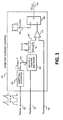
- Fig. 1 shows one example of a dc-dc power supply 100 that receives an input voltage V IN 105 to produce an output voltage Vo 140 and an output current I O 135 at a load 145.
- power supply 100 is an ac-dc power supply, where dc input voltage V IN 105 is a rectified and filtered ac input voltage received from an input voltage source (not shown).
- Input voltage V IN 105 is positive with respect to an input return 108.
- Output voltage Vo 140 is positive with respect to an output return 112.
- the dc-dc power supply 100 in the example of Fig. 1 includes a dc-dc converter 115 that is controlled by a controller 155 to regulate the output voltage Vo 140 and the output current I O 135.
- the controller 155 may be called a CV-CC controller because it may be utilized to control an output of the dc-dc converter 115 to have a constant voltage (CV) region and a constant current (CC) region.
- the dc-dc converter 115 typically includes at least one switch 120, at least one coupled inductor 125, and at least one capacitor 130.
- All standard converter configurations used to provide galvanically isolated outputs such as for example the flyback converter and for example the many variants of the buck converter may be realized by an arrangement of switches, coupled inductors, and capacitors represented by the dc-dc converter block 115 in the example of Fig. 1 .
- CV-CC controller 155 receives an I INSENSE signal 150 that is representative of the input current I IN 110, a V INSENSE signal 175 that is representative of the input voltage V IN 105, and a V OSENSE signal 180 that is representative of the output voltage Vo 140.
- a switch 120 included in dc-dc converter 115 is responsive to a CV OUT CC OUT signal 185 received from CV-CC controller 155.
- CV OUT CC OUT 185 is a logic signal that may be high or low within a switching period Ts.
- a switch 120 is closed when CV OUT CC OUT 185 is high, and the switch 120 is open when CV OUT CC OUT 185 is low.
- a closed switch is sometimes referred to as being in an on state.
- An open switched is sometimes referred to as being in an off state. In other words, a switch that turns on closes, and a switch that turns off opens.
- switch 120 is a metal oxide semiconductor field effect transistor (MOSFET).
- MOSFET metal oxide semiconductor field effect transistor
- CV-CC controller 155 may be implemented as a monolithic integrated circuit or may be implemented with discrete electrical components or a combination of discrete and integrated components.
- CV-CC controller 155 and switch 120 could form part of an integrated circuit that is manufactured as either a hybrid or a monolithic integrated circuit.
- a current sensor that produces I INSENSE signal 150 may also form part of the integrated circuit.
- the input current I IN 110 is a pulsating current that is substantially zero when CV OUT CC OUT signal 185 is low.
- the waveform of the input current I IN 110 may exhibit two distinct shapes. Each shape corresponds to a different mode of operation of the dc-dc converter 115.
- the dc-dc converter 115 is operating in discontinuous conduction mode (DCM).
- DCM discontinuous conduction mode
- the dc-dc converter 115 is operating in continuous conduction mode (CCM).
- the mode of operation depends on the input voltage V IN 105, the output voltage Vo 140, the load 145, and the particular design of the converter.
- the mode of operation typically changes from CCM to DCM as the input voltage V IN 105 increases, and it typically changes from DCM to CCM as the load increases.
- dc-dc converter 115 may be designed to operate in only CCM or in only DCM within a restricted range of input voltage and load. Examples, in accordance with the present invention, allow a single design to provide the desired regulation of output voltage and output current for DCM and CCM operation.
- the CV-CC controller 155 in the example of Fig. 1 includes a constant current control circuit 160, a constant voltage control circuit 170, and a logic circuit 165.
- the constant current control circuit 160 and the constant voltage control circuit 170 receive the input current sense signal I INSENSE 150, the input voltage sense signal V INSENSE 175, and the output voltage sense signal V OSENSE 180.
- input voltage sense signal V INSENSE 175 and output voltage sense signal V OSENSE 180 may be any signals that have a known relationship to the input voltage V IN 105 and the output voltage Vo 140 respectively. In other words, it is not necessary to sense the input voltage directly or the output voltage directly to obtain the respective signals V INSENSE 175 and V OSENSE 180.
- the signal V INSENSE 175 may be a timing signal that is high while current in an inductor is greater than a first value while being less than a second value.
- V INSENSE 175 may represent the amount of time that it takes current in the inductor to change from the first value to the second value. In one example, V INSENSE 175 may represent the average value of a digital signal, where the digital signal is high during the time that it takes the current in an inductor to change from the first value to the second value so that a value of input voltage V IN 105 can be derived.
- Constant current control circuit 160 produces a control signal 190 to operate dc-dc converter 115 in the regulated output current region.
- Constant voltage control circuit 170 produces a control signal 195 to operate dc-dc converter 115 in the regulated output voltage region.
- Logic circuit 165 responds to control signals 195 and 190 to produce an appropriate CV OUT CC OUT signal 185 to control the switch 120 in dc-dc converter 115 for a regulated voltage region and a regulated current region as illustrated by the graph in Fig. 2 .
- Fig. 2 is an example graph of an output characteristic 200 of a power supply that has a region of regulated output voltage 210 and a region of regulated output current 220.
- Output characteristic 200 is one possible output characteristic of power supply 100 of Fig. 1 .
- the example shows that the output voltage Vo 140 is a substantially constant regulated value V REG 230 when the output current I O 135 is less than a threshold current that in one example may be a regulated value I REG 240.
- the example also shows that the output current I O 135 is a substantially constant regulated value I REG 240 when the output voltage Vo 140 is less than a threshold voltage value and greater than an optional auto-restart voltage V AR 260.
- the threshold voltage value may be the regulated value V REG 230.
- the regulated current region 220 it is not desirable to extend the regulated current region 220 to an output voltage of zero volts.
- power supplies that charge batteries do not normally have an output voltage of zero volts since even a fully discharged battery exhibits a minimum voltage when it is charging. Therefore, output voltage less than a minimum value indicates a failure of the battery, and the power supply typically is required to deliver substantially less than the regulated current under such circumstances.
- a power supply may enter an auto-restart mode when the output voltage is below a minimum value to guarantee that the average output current does not exceed a maximum desired value.
- a power supply When operating in an auto-restart mode, a power supply will typically deliver its maximum output current for a time that is long enough to raise the output voltage above the auto-restart value V AR 260 under normal circumstances. If the output voltage is not above the auto-restart value V AR 260 after an allotted time, then the power supply typically will deliver no output current for a substantially long time that may be hundreds or thousands of switching periods before repeating the delivery of maximum output current.
- the characteristic of the load 145 determines where the power supply will operate on the graph of the output characteristic 200.
- the output will be a regulated voltage with value V REG 230.
- logic circuit 165 selects control signal 195 from constant voltage control circuit 170 to control the switch 120 of the dc-dc converter 115.
- the power from the output will increase until the power reaches the design limit of the dc-dc converter 115.
- the design limit of the dc-dc converter 115 corresponds to a maximum output power 250.
- Logic circuit 165 detects the response of constant voltage control circuit 170 to the reduction in output voltage Vo 230, and selects the control signal 190 from constant current control circuit 160 to regulate the output current I O 135 to the value I REG 240 until the output voltage falls to the auto-restart value V AR 260 at the point 270 on the graph.
- the constant voltage control circuit 170 in the example power supply 100 of Fig. 1 may use any of several techniques known in the art for regulation of the output voltage of a power supply. Examples of these techniques include pulse width modulation (PWM) with constant switching frequency, PWM with variable switching frequency, pulse frequency modulation (PFM) with fixed pulse width, and on/off control.
- Pulse width modulation is a technique that changes the length of time a switch conducts during a switching period.
- the switching period may be either constant or variable. When the switching period is constant, both the length of time the switch conducts and the length of time the switch does not conduct must change. When the switching period is variable, the length of time the switch conducts and the length of time the switch does not conduct may change independently.
- Pulse frequency modulation is a technique that changes the length of time the switch is off while maintaining the on-time substantially constant.
- On/off control is a technique that either allows a switch to conduct or prevents a switch from conducting during a switching period, producing a sequence of regular switching periods where the switch conducts in some switching periods and the switch does not conduct in other switching periods.
- examples of the present invention may be used with many different techniques to regulate output voltage.
- Examples of the invention described in this disclosure may also use many techniques to sense the input current I IN 110 as the current sense signal I INSENSE 150.
- Current sensor symbol 114 in Fig. 1 may represent any of the many known ways to sense current.
- the input current may be sensed as a voltage on a discrete resistor, or as a current from a current transformer, or as a voltage across the on-resistance of a metal oxide semiconductor field effect transistor (MOSFET) when the input current is the same as the current in the transistor, or as a current from the sense output of a current sensing field effect transistor (senseFET).
- MOSFET metal oxide semiconductor field effect transistor
- the output voltage sense signal V OSENSE 180 may be obtained directly from a measurement of the output voltage Vo 140 with respect to the output return 112 in examples where galvanic isolation is not required, or in examples where the cost of electro-optical isolation is acceptable. It is appreciated that direct sensing of the output voltage Vo 140 typically will provide a smaller deviation from the desired value V REG 230 in the region of constant output voltage 210 than can be achieved with indirect sensing.
- the output voltage sense signal V OSENSE 180 may be obtained by either indirect or direct sensing methods.
- Examples of the present invention provide an output with a regulated current region 220 in the absence of a direct measurement of the output current I O 135. This is accomplished by making use of the mathematical relationship between various signal values as explained below:
- the average input power is identical to the average output power.
- a dc-dc converter such as the example of Fig.
- Equation (2) represents the total electric charge Q taken from the input voltage source (and received by the dc-dc converter) over the switching period Ts.
- Equation (5) shows that the electric charge taken from the source of input voltage 105 during each switching period is directly proportional to the output voltage Vo and inversely proportional to the input voltage V IN .
- the charge relationship of Equation (5) may be converted to a voltage relationship by dividing both sides of Equation (5) by a capacitance C.
- the charge Q may be determined from either integration of the input current I IN 110 or integration of the current sense signal I INSENSE 150.
- the right hand side of Equation (6) may be presented in terms of the sensed quantities V OSENSE and V INSENSE , with the scaling factors being accounted for in a scaling voltage V K , where V K is given in Equation (8) below.
- V Q is the integrated signal that represents the electric charge received by the dc-dc converter within a switching period Ts and V K is a scaling voltage.
- Equation (7) may be used in a control circuit in a number of ways to control a dc-dc converter that has an output with a region of constant current.
- Fig. 3 illustrates one example of a constant current control circuit 310 in accordance with the teaching of the invention.
- a resettable integrator 320 integrates the input current sense signal I INSENSE 150 while the switch 120 in the dc-dc converter 115 is closed.
- Resettable integrator 320 produces an integrated signal V Q 330 that in one example is a voltage proportional to the charge taken from the source of input voltage V IN 105 during switching period Ts. Therefore, the integrated signal V Q 330 may be referred to as a charge signal.
- a multiplier 360 produces a multiplication signal 340 that is the product of the charge signal V Q 330 and the input voltage sense signal V INSENSE 175 scaled by the scaling voltage V K .
- a clock signal 390 goes high to set a latch 380 at the beginning of a switching period Ts.
- An output of latch 380 is a control signal CC OUT 190 that goes high when latch 380 is set.
- Control signal CC OUT 190 goes low when latch 380 is reset.
- the output of a comparator 370 goes high to reset latch 380 to open switch 120 when the multiplication signal 340 becomes greater than the V OSENSE signal 180.
- resettable integrator 320 is reset on the falling edge of control signal CC OUT 190.
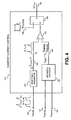
- the example circuit of Fig. 4 shows an alternative constant current control circuit 410 that produces the CC OUT signal in a different manner as the example controller of Fig. 3 .
- the example constant current control circuit 410 includes an arithmetic operator circuit 420 that performs multiplication, division, and scaling of the input voltage sense signal V INSENSE 175 and the output voltage sense signal V OSENSE 180 that is scaled by the scaling voltage V K .
- the output 430 of arithmetic operator circuit 420 is a reference signal V QREF that is equal to the term on the right-hand side of Equation (7)
- V QREF V OSENSE V INSENSE ⁇ V K
- arithmetic operator 420 is coupled to divide the output voltage sense signal by the input voltage sense signal and to scale the result by a scaling factor V K to generate the reference signal V QREF .
- clock signal 390 goes high to set a latch 380 at the beginning of switching period Ts.
- An output of latch 380 is a control signal CC OUT 190 that goes high when latch 380 is set. Control signal CC OUT 190 goes low when latch 380 is reset.
- comparator 370 goes high to reset latch 380 to open switch 120 when the charge signal V Q 330 becomes greater than the V QREF signal 430, which in the illustrated example is proportional to a ratio of the output voltage to the input voltage.
- constant current control circuit 410 generates control signal CC OUT 190 to control switching of switch 120 to regulate an output current of the power supply such that charge signal V Q 330 is proportional to a ratio of output voltage sense signal V OSENSE 180 to the input voltage sense signal V INSENSE 175.
- the example resettable integrator 320 of Figs. 3 and 4 may include a capacitor, a current source to charge the capacitor, and a switch to discharge the capacitor.
- resettable integrator 320 may be a two-way integrator. That is, resettable integrator 320 may integrate current sense signal I INSENSE 150 by charging a capacitor during one switching period Ts and may then integrate current sense signal I INSENSE 150 by discharging the capacitor in a subsequent switching period.
- Such a two-way integrator may be useful in applications in which a high maximum duty ratio (e.g., 99%-100%) is desired for control signal CC OUT 190.
- An example resettable integrator circuit is discussed later in this disclosure.
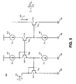
- Fig. 5 shows an example circuit 500 that may perform the functions of the multiplier 360 of Fig 3 and also the functions of the arithmetic operator 420 of Fig. 4 in accordance with the teaching of the invention.
- bipolar NPN transistors 530, 520, 525, and 555 are matched.
- the base to emitter voltage of a bipolar transistor is directly proportional to the natural logarithm of the collector current.
- V BE is the base to emitter voltage
- V T is the thermal voltage fixed by physical constants
- Ic is the collector current
- Is is the reverse saturation current of the base to emitter junction of the transistor.
- I Y I C ⁇ 2 I C ⁇ 3 ⁇ I X
- application of the logarithmic relationship of Equation (11) to the circuit of Fig. 5 shows that the input current Ix 505 is multiplied by the value I C2 of current sources 510 and 535. It can also be shown that the input current Ix 505 is divided by the value I C3 of the current sources 515 and 540.
- multiplication of two signals may be achieved by the circuit in Fig. 5 when Ix 505 is proportional to a first signal while current sources 510 and 535 are proportional to a second signal.
- Multiplication by the reciprocal of a third signal may be achieved when the current sources 515 and 540 are proportional to the third signal.
- Many suitable variants of the example circuit of Fig. 5 are known in the art.
- current sources I C2 510 and 535 are constant with a value representative of the scaling voltage V K
- current sources I C3 515 and 540 are variable current sources controlled by the input voltage sense signal V INSENSE 175.
- output current I Y is representative of the reference signal V QREF 430, in accordance with Equation (10).
- Fig. 6 is a schematic diagram 600 of another circuit that may provide the signal V QREF 430 in the constant current control circuit 410 of the example of Fig. 4 .
- the example circuit of Fig. 6 has the desirable feature that it does not require matched bipolar transistors to achieve the desired accuracy in the result.
- the example circuit of Fig. 6 uses the principle that the time required for a signal that is changing at a constant rate to go between two fixed values is inversely proportional to the rate of the change. Conversely, a signal changing at a constant rate for a fixed time will change by an amount that is directly proportional to the rate of change. It will be demonstrated next how the circuit of Fig. 6 uses time, rates of change, and fixed values to produce the reference signal V QREF 430 that is directly proportional to the output voltage V O 140 and is inversely proportional to the input voltage V IN 105.
- the example circuit of Fig. 6 includes an oscillator 675 that provides timing signals for the operation of the power supply.
- Fig. 7 is a timing diagram 700 of signals in the circuit 600.
- a convenient reference signal for timing purposes is the D MAX signal 680.
- D MAX signal 680 is low between time to 740 and time t 3 730.
- D MAX signal 680 is high between time t 3 730 and time t 4 750.
- Switch 120 may be closed when D MAX 680 is high. Switch 120 must be open when D MAX 680 is low. Therefore, D MAX is high for the maximum on-time T ONMAX of switch 120.
- the example circuit of Fig. 6 includes a variable current source 605 that has a current directly proportional to input voltage V IN 105.
- the ratio of the input voltage V IN 105 to the current of current source 605 is the resistance R VIN .
- Current source 605 is controlled by input voltage sense signal V INSENSE 175 in the example of Fig. 6 .
- the example circuit of Fig. 6 also includes a variable current source 615 that has a current directly proportional to output voltage Vo 140.
- the ratio of the output voltage Vo 140 to the current of current source 615 is the resistance R VO .
- Current source 615 is controlled by output voltage sense signal V OSENSE 180 in the example of Fig. 6 .
- RESET signal 670 is high until a time t 1 720 after D MAX 680 goes low.
- Resettable integrators 685 and 690 are reset when RESET signal 670 goes high.
- Fig. 7 illustrates capacitors C RAMP 640 and C T&H 665 being reset to zero volts, in one example, capacitors C RAMP 640 and C T&H 665 are reset to a non-zero voltage such that the charging from current sources 605 and 615, respectively, occurs in a linear operating range of capacitors C RAMP 640 and C T&H 665.
- Fig. 7 illustrates capacitors C RAMP 640 and C T&H 665 being reset to zero volts
- capacitors C RAMP 640 and C T&H 665 are reset to a non-zero voltage such that the charging from current sources 605 and 615, respectively, occurs in a linear operating range of capacitors C RAMP 640 and C T&H 665.
- a SET signal 655 goes high on the falling edge of RESET signal 670.
- the rising edge of SET signal 655 sets flip-flop 675.
- the TRACK signal 650 at the output of flip-flop 675 goes high, allowing n-channel transistor 645 to conduct current from current source 615.
- p-channel transistor 695 When D MAX 680 is low, p-channel transistor 695 conducts current from current source 605.
- RESET signal 670 goes low at time t 1 710, n-channel transistor 635 of resettable integrator 685 stops conducting to allow capacitor C RAMP 640 of resettable integrator 685 to charge from current source 605 through p-channel transistor 695.
- n-channel transistor 660 of resettable integrator 690 stops conducting to allow track and hold capacitor C T&H 665 to charge from current source 615 through n-channel transistor 645. The charging of capacitor C T&H 665 produces a voltage V T&H 430.
- capacitor C RAMP 640 produces a voltage V RAMP 610 that is compared to an arbitrary reference voltage V A 620 by comparator 625.
- the voltage V RAMP 610 becomes greater than the voltage V A 620 at the time t 2 720, causing the output 630 of comparator 625 to reset flip-flop 675.
- TRACK signal 650 goes low to stop current source 615 from charging track and hold capacitor C T&H 665.
- V QREF V O V IN ⁇ R VIN R VO ⁇ C RAMP C T & H ⁇ V A
- the values of R VIN , Rvo, C RAMP , C T&H , and V A may be selected to meet the requirement of Equation (7). Therefore, the example circuit 600 of Fig. 6 integrates two signals for a duration of time to provide a value V QREF within a switching period Ts that is directly proportional to a value representative of output voltage Vo 140 and is inversely proportional to a value representative of input voltage V IN 105.
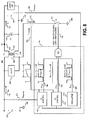
- Fig. 8 shows one example of a power supply 800 that includes a particular dc-dc converter known as a flyback converter.
- the example flyback converter of Fig. 8 includes an energy transfer element that is a coupled inductor T1 125, sometimes referred to as a transformer.
- Coupled inductor T1 125 has a primary winding 820 that is coupled to the source of input voltage V IN 105.
- Coupled inductor T1 125 has a secondary winding 825 that is coupled to the output return 112.
- a switch S1 120 coupled to one end of primary winding 820 opens and closes in response to a drive signal 185 from controller 155.
- switch S1 120 may be a metal oxide semiconductor field effect transistor (MOSFET).
- switch S1 120 may be a bipolar junction transistor (BJT).
- switch S1 120 may be an insulated gate bipolar transistor (IGBT).
- a clamp circuit 805 is coupled across the primary winding 820 to limit the voltage across primary winding 820 when switch S1 120 opens.
- controller 155 In the example power supply of Fig. 8 , controller 155 generates a drive signal 185 in response to an input voltage sense signal 175, an output voltage sense signal 180, and an input current sense signal 150.
- Input current sense signal 150 is representative of the value of current I D 815 in switch S1 120.
- the current I D 815 is the same as the input current I IN 110 when switch S1 120 is closed. Any of the several ways practiced in the art to sense current in a switch may provide the current sense signal 150.
- the waveform of the input current sense signal 150 in the example of Fig. 8 shows that the power supply is operating in continuous conduction mode.
- the switching of switch S1 120 produces a pulsating current in secondary winding 825.
- the current in secondary winding 825 is rectified by diode D1 810 and filtered by capacitor C1 130 to produce a substantially dc output voltage Vo 140 and an output current Io 135 to a load 145.
- Fig. 8 illustrates a power supply 800 that is operating in a region of regulated output current 220 as shown in the graph of Fig. 2 .
- the output voltage Vo 140 in the example of Fig. 8 is below the regulated value V REG 230. Therefore, constant voltage control circuit 170 produces an output CV OUT 195 that is always high.
- Oscillator 675 produces signal D MAX 680 that is high for time T ONMAX
- constant current control circuit 160 produces a control signal CC OUT 190 that is high for a time T ONCC that is less than T ONMAX .
- Logic circuit 165 is an AND gate that receives the signals CC OUT 190, CV OUT 195, and D MAX 680 in the example of Fig. 8 to produce the drive signal 185. Since all inputs to AND gate 165 must be high to produce a high output 185, switch S1 120 in the example power supply of Fig. 8 operates under the control of constant current control circuit 160.
- Fig. 9 illustrates a flyback power supply 900 that is operating in a region of regulated output voltage 210 as shown in the graph of Fig. 2 .
- the output current Io 135 in the example of Fig. 9 is below the regulated value I REG 240. Therefore, constant current control circuit 160 produces an output signal CC OUT 190 that is always high.
- Oscillator 675 produces signal D MAX 680 that is high for a time T ONMAX
- constant voltage control circuit 170 produces a signal CV OUT 195 that is high for a time T ONCV that is less than T ONMAX . Since all inputs to AND gate 165 must be high to produce a high output 185, switch S1 1 120 in the example power supply of Fig. 9 operates under the control of constant voltage control circuit 170.
- Fig. 10 is an example of a flyback power supply 1000 that includes a coupled inductor T1 1005 that has three windings. Coupled inductor T1 1005 includes a winding 1010 that provides a voltage V B .
- the voltage V B on winding 1010 is an ac voltage with an average voltage of zero.
- a positive voltage on winding 1010 with respect to the input return 108 is representative of the output voltage Vo 140
- a negative voltage on winding 1010 with respect to the input return 108 is representative of the input voltage V IN 105. Therefore, a signal 1015 from winding 1010 may combine an input voltage sense signal V INSENSE 175 and an output voltage sense signal V OSENSE 180.
- the combined voltage sense signal 1015 may be received by a controller 155.
- the example of Fig. 10 shows waveforms of the input current sense signal I INSENSE 150 and the combined voltage sense signal 1015 that indicate the example power supply is operating in discontinuous conduction mode. It is appreciated that the power supply 1000 of Fig. 10 may operate in continuous conduction mode when input voltage V IN 105 decreases or when output current I O 135 increases.
- Fig. 11 shows an example schematic 1100 that includes an addition to the example circuit 600 of Fig. 6 for use with the combined voltage sense signal 1015 of the example power supply of Fig. 10 .
- the example of Fig. 11 includes a signal separator circuit 1105 that extracts the V INSENSE signal 175 and the V OSENSE signal 180 from the combined voltage sense signal 1015.
- signal separator circuit 1105 rectifies the combined voltage sense signal 1015.
- the rectified signal is sampled and held to produce V INSENSE 175 when CV OUT CC OUT 185 goes high, and the rectified signal is sampled and held to produce V OSENSE 180 when CV OUT CC OUT goes low.
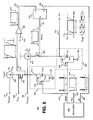
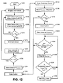
- Fig. 12 is a flowchart 1200 that describes a method to control the example power supply of Fig. 10 that has an output with a region of regulated voltage and a region of regulated current according to the teaching of the invention.
- step 1206 After starting in step 1202 with an output voltage of zero and no output current, auto-restart operation is engaged in step 1204. While in the auto-restart mode, step 1206 stores the value of V INSENSE when the switch S1 120 is closed, and step 1208 stores the value of V OSENSE when switch S1 120 is open.
- Step 1210 compares output voltage Vo 140 to the auto-restart threshold voltage V AR 260. If output voltage V O 140 is greater than the auto-restart threshold voltage V AR 260, then auto-restart ends in step 1212. If output voltage Vo 140 is not greater than the auto-restart threshold voltage V AR 260, then auto-restart continues in step 1206.
- step 1214 After the end of auto-restart in step 1212, a new switching period begins in step 1214.
- the integrator of input current sense signal I INSENSE 150 is reset to an initial value in step 1216.
- Step 1218 compares output voltage Vo 140 to the regulated value V REG 230. If output voltage Vo 140 is less than the regulated value V REG 230, then switch S1 120 closes in step 1220. If output voltage Vo 140 is not less than the regulated value V REG 230, then switch S1 120 remains open in step 1232, the value of V OSENSE 180 is stored in step 1234, and output voltage Vo 140 is compared to the auto-restart threshold voltage V AR 260 in step 1236.
- step 1236 If output voltage Vo 140 is less than the auto-restart threshold voltage V AR 260 in step 1236, then the flow returns to step 1204 to engage auto-restart. If output voltage Vo 140 is not less than the auto-restart threshold voltage V AR 260 in step 1236, then the controller waits for the end of the switching period in step 1238 before another switching period begins in step 1214.
- step 1222 stores the value of V INSENSE 175.
- the collective status of the signals D MAX 680, CV OUT 195, and CC OUT 190 is then evaluated in step 1224. If D MAX 680, CV OUT 195, and CC OUT 190 are all at a logic high level, then the integration of input current sense signal I INSENSE 150 begins in step 1226. If any of the signals D MAX 680, CV OUT 195, and CC OUT 190 are at a logic low level, then switch S1 120 opens in step 1232.
- V Q 330 is compared to the reference value V QREF 430 in step 1228. If V Q 330 is less than V QREF 430, then the flow returns to step 1224. If V Q 330 is not less than V QREF 430, then CC OUT 190 is set to a logic low level in step 1230 before the flow returns to step 1224.
Claims (15)
- Ein Controller (155) für ein Stromversorgungsgerät (100), der Controller umfassend:eine Gleichstromsteuerschaltung (160, 310, 410) gekoppelt, um ein Eingangsstrommesssignal (150), ein Eingangsspannungsmesssignal (175) und ein Ausgangsspannungsmesssignal (180) zu empfangen, und dazu ausgelegt, einen Ausgangsstrom (135) des Stromversorgungsgeräts (100) durch Generieren eines Steuersignals (185) zu regeln, um Schalten eines Schalters (120) des Stromversorgungsgerät (100) zu steuern;gekennzeichnet dadurch, dassder Controller einen rücksetzbaren Integrator (320) umfasst, der in der Gleichstromsteuerschaltung (160, 310, 410) enthalten ist, und der gekoppelt ist, das Eingangsstrommesssignal (150) während einer Schaltperiode des Steuersignals (185) zu integrieren, um ein integriertes Signal (330) zu generieren, das repräsentativ ist für eine Ladung, die von einer Eingangsspannungsquelle (105) des Stromversorgungsgeräts (100) entnommen wurde, wobei die Gleichstromsteuerschaltung (160, 310, 410) dazu ausgelegt ist, das Schalten des Schalters (120) zu steuern, so dass das integrierte Signal (330) proportional ist zu einem Verhältnis des Ausgangsspannungsmesssignals (180) zum Eingangsspannungsmesssignal (175).
- Der Controller (155) nach Anspruch 1, wobei das Steuersignal (185) ein erstes Steuersignal (185) ist, wobei der Controller weiter umfasst eine Gleichspannungssteuerschaltung, um ein zweites Steuersignal in Antwort auf das Ausgangsspannungsmesssignal (180) zu generieren, um Schalten des Schalters (120) zu steuern, um eine Ausgangsspannung des Stromversorgungsgeräts (100) zu regulieren.
- Der Controller (155) nach Anspruch 2, weiter umfassend eine Logikschaltung gekoppelt an die Gleichspannungssteuerschaltung, um Schalten des Schalters (120) zu steuern, in Antwort auf das zweite Steuersignal, um die Ausgangsspannung des Stromversorgungsgerät (100) zu regulieren, wenn der Ausgangsstrom geringer ist als ein Schwellstrom, und wobei die Logikschaltung gekoppelt ist an die Gleichstromsteuerschaltung (160, 310, 410), um Schalten des Schalters (120) in Antwort auf das erste Steuersignal zu steuern, um den Ausgangsstrom zu regulieren, wenn die Ausgangsspannung geringer ist als eine Schwellspannung.
- Der Controller (155) nach Anspruch 3, weiter umfassend einen Oszillator (675), um ein Signal für die maximale Einschaltdauer zu generieren, wobei ein erster Eingang der Logikschaltung gekoppelt ist, um das erste Steuersignal zu empfangen, und wobei ein zweiter Eingang der Logikschaltung gekoppelt ist, um das zweite Steuersignal zu empfangen, und wobei ein dritter Eingang der Logikschaltung gekoppelt ist, um ein Signal für die maximale Einschaltdauer zu empfangen.
- Der Controller (155) nach Anspruch 3, wobei die Ausgangsspannung auf die Schwellspannung reguliert wird, wenn die Ausgangsspannung reguliert wird, und wobei der Ausgangsstrom auf den Schwellstrom reguliert wird, wenn der Ausgangsstrom reguliert wird.
- Der Controller (155) nach Anspruch 1, wobei der Controller den Schalter (120) von einem AN-Zustand in einen AUS-Zustand schaltet in Antwort darauf, dass das integrierte Signal (330) einen Wert erreicht, der proportional ist zu dem Verhältnis des Ausgangsspannungsmesssignals (180) zum Eingangsspannungsmesssignal (175).
- Der Controller (155) nach Anspruch 1, wobei die Gleichstromsteuerschaltung (160, 310, 410) weiter eine arithmetische Operatorschaltung (420) umfasst, die gekoppelt ist, um das Eingangsspannungsmesssignal (175) zu multiplizieren, zu dividieren oder zu skalieren.
- Der Controller (155) nach Anspruch 7, wobei die arithmetische Operatorschaltung (420) gekoppelt ist, um das Ausgangsspannungsmesssignal (180) durch das Eingangsspannungsmesssignal (175) zu dividieren, um ein Referenzsignal zu generieren, wobei die Gleichstromsteuerschaltung (160, 310, 410) weiter einen Komparator umfasst, der einen ersten Eingang hat, der gekoppelt ist, um das Referenzsignal zu empfangen, der einen zweiten Eingang hat, der gekoppelt ist, um das integrierte Signal (330) zu empfangen, und der einen Ausgang hat, der gekoppelt ist, um das Steuersignal (185) auszugeben.
- Der Controller (155) nach Anspruch 7, wobei die arithmetische Operatorschaltung (420) gekoppelt ist, um das Eingangsspannungsmesssignal (175) mit dem integrierten Signal (330) zu multiplizieren, um ein Multiplikationssignal zu generieren, wobei die Gleichstromsteuerschaltung (160, 310, 410) weiter einen Komparator umfasst, der einen ersten Eingang hat, der gekoppelt ist, um das Referenzsignal zu empfangen, der einen zweiten Eingang hat, der gekoppelt ist, um das Ausgangsspannungsmesssignal (180) zu empfangen, und der einen Ausgang hat, der gekoppelt ist, um das Steuersignal (185) auszugeben.
- Der Controller (155) nach Anspruch 1, weiter umfassend:eine erste variable Stromquelle, die durch das Eingangsspannungsmesssignal (175) gesteuert wird, um einen ersten Strom zu generieren;einen ersten Integrator gekoppelt, um den ersten Strom zu integrieren, um ein Rampenspannungssignal zu generieren;eine zweite variable Stromquelle, die durch das Ausgangsspannungsmesssignal (180) gesteuert wird, um einen zweiten Strom zu generieren;einen zweiten Integrator gekoppelt, um den zweiten Strom zu integrieren, wenn der Schalter (120) in einem AUS-Zustand ist, um eine Track-and-Hold-Spannung bereit zu stellen, wobei die Track-and-Hold-Spannung proportional ist zu einem Verhältnis des Ausgangsspannungsmesssignals (180) zum Eingangsspannungsmesssignal (175) zu einer Zeit, bei der das Rampenspannungssignal eine Referenzspannung erreicht;einen Komparator, der einen ersten Eingang hat, der gekoppelt ist, um die Track-and-Hold-Spannung zu empfangen, der einen zweiten Eingang hat, der gekoppelt ist, um das integrierte Signal (330) zu empfangen, und der einen Ausgang hat, der gekoppelt ist, um das Steuersignal (185) auszugeben.
- Der Controller (155) nach Anspruch 1, weiter umfassend:ein Eingangsterminal gekoppelt, um ein kombiniertes Spannungsrichtungssignal zu empfangen, das repräsentativ ist für die Eingangsspannung und die Ausgangsspannung des Stromversorgungsgeräts (100); undein Signalseparator gekoppelt zwischen das Eingangsterminal und die Gleichstromsteuerschaltung (160, 310, 410), um das kombinierte Spannungsmesssignal in das Eingangsspannungsmesssignal (175) und das Ausgangsspannungsmesssignal (180) zu trennen.
- Der Controller (155) nach Anspruch 1, wobei der Schalter (120) und die Gleichstromsteuerschaltung (160, 310, 410) integriert sind in ein einzelnes monolithisches Bauteil.
- Der Controller (155) nach irgendeinem der vorhergehenden Ansprüche, wobei der rücksetzbare Integrator (320) das Eingangsstrommesssignal (150) integriert, während der Schalter (120) geschlossen ist, wobei das integrierte Signal (330) eine Spannung ist, die proportional ist zu einer Ladung, die von einer Eingangsspannungsquelle (105) während einer Schaltperiode (Ts) entnommen wurde.
- Der Controller (155) nach irgendeinem der vorhergehenden Ansprüche, wobei der rücksetzbare Integrator (320) ein Zweiwegeintegrator ist, der das Eingangsstrommesssignal (150) integriert durch Laden eines Kondensators während einer Schaltperiode (Ts), und der dann das Eingangsstrommesssignal (150) integriert durch Entladen des Kondensators in einer nachfolgenden Schaltperiode.
- Der Controller (155) nach irgendeinem der vorhergehenden Ansprüche, wobei der Controller (155) für ein Stromversorgungsgerät (100) fähig ist, einen galvanisch isolierten Ausgang bereit zu stellen, der einen Bereich regulierter Spannung und einen Bereich regulierten Stroms hat.
Priority Applications (1)
| Application Number | Priority Date | Filing Date | Title |
|---|---|---|---|
| EP12184866A EP2538536A2 (de) | 2009-06-02 | 2010-05-18 | Vorrichtung zur Steuerung der Eingangsladung einer Stromversorgung |
Applications Claiming Priority (1)
| Application Number | Priority Date | Filing Date | Title |
|---|---|---|---|
| US12/477,058 US8139384B2 (en) | 2009-06-02 | 2009-06-02 | Method and apparatus for input charge control of a power supply |
Related Child Applications (1)
| Application Number | Title | Priority Date | Filing Date |
|---|---|---|---|
| EP12184866A Division-Into EP2538536A2 (de) | 2009-06-02 | 2010-05-18 | Vorrichtung zur Steuerung der Eingangsladung einer Stromversorgung |
Publications (2)
| Publication Number | Publication Date |
|---|---|
| EP2259418A1 EP2259418A1 (de) | 2010-12-08 |
| EP2259418B1 true EP2259418B1 (de) | 2014-10-29 |
Family
ID=42634760
Family Applications (2)
| Application Number | Title | Priority Date | Filing Date |
|---|---|---|---|
| EP12184866A Withdrawn EP2538536A2 (de) | 2009-06-02 | 2010-05-18 | Vorrichtung zur Steuerung der Eingangsladung einer Stromversorgung |
| EP10163150.5A Not-in-force EP2259418B1 (de) | 2009-06-02 | 2010-05-18 | Vorrichtung zur Steuerung der Eingangsladung einer Stromversorgung |
Family Applications Before (1)
| Application Number | Title | Priority Date | Filing Date |
|---|---|---|---|
| EP12184866A Withdrawn EP2538536A2 (de) | 2009-06-02 | 2010-05-18 | Vorrichtung zur Steuerung der Eingangsladung einer Stromversorgung |
Country Status (4)
| Country | Link |
|---|---|
| US (4) | US8139384B2 (de) |
| EP (2) | EP2538536A2 (de) |
| JP (1) | JP5693877B2 (de) |
| CN (2) | CN103475228B (de) |
Families Citing this family (35)
| Publication number | Priority date | Publication date | Assignee | Title |
|---|---|---|---|---|
| JP5349905B2 (ja) * | 2008-10-27 | 2013-11-20 | パナソニック株式会社 | 放電灯点灯装置、及びこれを用いた車両用前照灯点灯装置 |
| JP2010200450A (ja) * | 2009-02-24 | 2010-09-09 | Fujitsu Semiconductor Ltd | 半導体集積回路および電源装置 |
| US8098506B2 (en) | 2009-06-02 | 2012-01-17 | Power Integrations, Inc. | Single-stage power supply with power factor correction and constant current output |
| US7965151B2 (en) * | 2009-06-02 | 2011-06-21 | Power Integrations, Inc. | Pulse width modulator with two-way integrator |
| US8139384B2 (en) * | 2009-06-02 | 2012-03-20 | Power Integrations, Inc. | Method and apparatus for input charge control of a power supply |
| US8593839B2 (en) * | 2009-09-17 | 2013-11-26 | Linear Technology Corporation | Accuracy of a volt-second clamp in an isolated DC-DC converter |
| US8384443B2 (en) * | 2011-01-27 | 2013-02-26 | Maxim Integrated Products, Inc. | Current mirror and current cancellation circuit |
| US8963529B2 (en) * | 2011-04-28 | 2015-02-24 | Texas Instruments Incorporated | Transition mode charge control for a power converter |
| US8779746B2 (en) | 2011-04-29 | 2014-07-15 | Texas Instruments Incorporated | Methods and apparatus for constant power/current control for switch-mode power converters |
| CN102185502B (zh) * | 2011-05-06 | 2013-04-03 | 上海新进半导体制造有限公司 | 开关电源控制器的恒流输出控制电路及开关电源 |
| CN102290972B (zh) * | 2011-08-15 | 2014-03-19 | 成都芯源系统有限公司 | 开关电源及其控制电路和控制方法 |
| JP5738777B2 (ja) * | 2012-01-23 | 2015-06-24 | 株式会社日本自動車部品総合研究所 | 電力変換装置 |
| JP5804476B2 (ja) * | 2012-01-25 | 2015-11-04 | 富士電機株式会社 | 充電装置 |
| JP5804477B2 (ja) * | 2012-01-25 | 2015-11-04 | 富士電機株式会社 | 充電装置 |
| CN102570837B (zh) * | 2012-02-28 | 2014-09-03 | 矽力杰半导体技术(杭州)有限公司 | 一种恒压恒流控制电路及其控制方法 |
| CN103312180B (zh) * | 2012-03-12 | 2016-06-08 | 致茂电子(苏州)有限公司 | 交流换流器中的定电流模式控制器 |
| CN102624254B (zh) * | 2012-03-26 | 2014-06-18 | 矽力杰半导体技术(杭州)有限公司 | 一种具有改进的负载调节的恒压恒流控制电路及其控制方法 |
| JP2014092370A (ja) * | 2012-10-31 | 2014-05-19 | Agilent Technologies Inc | 電圧電流特性発生器 |
| US8964412B2 (en) * | 2012-10-31 | 2015-02-24 | Power Integrations, Inc. | Split current mirror line sensing |
| KR101451009B1 (ko) | 2013-03-27 | 2014-10-15 | 주식회사 엘지씨엔에스 | 직렬 연결된 다수 개의 전지 직류 마이크로그리드 충방전 시스템 |
| KR101470735B1 (ko) * | 2013-05-15 | 2014-12-08 | 주식회사 엘지씨엔에스 | 직렬 연결된 다수의 2차 전지 충방전을 위한 능동 벨런스회로와 알고리즘을 구비한 2차 전지 충방전 제어장치 및 방법 |
| FR3008258B1 (fr) * | 2013-07-04 | 2018-11-02 | Safran Electronics & Defense | Convertisseur ac/dc a isolement galvanique et correcteur de signal |
| US9490707B2 (en) * | 2013-11-26 | 2016-11-08 | Telefonaktiebolaget L M Ericsson (Publ) | Control circuit and a method for an energy based pulse skipping mode in a DC/DC converter |
| US9397560B2 (en) | 2014-08-15 | 2016-07-19 | Power Integrations, Inc. | Controller for a power supply with transition region regulation |
| US9431895B2 (en) * | 2014-09-22 | 2016-08-30 | Shanghai Sim-Bcd Semiconductor Manufacturing Co., Ltd. | High power-factor control circuit and power supply |
| US9621019B2 (en) * | 2014-11-07 | 2017-04-11 | Power Intergrations, Inc. | Indirect regulation of output current in power converter |
| US9774248B2 (en) * | 2014-11-10 | 2017-09-26 | Power Integrations, Inc. | Introducing jitter to a switching frequency by way of modulating current limit |
| US9584008B2 (en) * | 2015-06-26 | 2017-02-28 | Dialog Semiconductor Inc. | Switching power converter with adaptive power factor correction |
| TWI636650B (zh) * | 2017-03-17 | 2018-09-21 | 通嘉科技股份有限公司 | 應用於電源轉換器的控制器及其操作方法 |
| CN109149935B (zh) * | 2018-09-07 | 2020-10-23 | 深圳市德赛微电子技术有限公司 | 一种开关电源不同工作模式自由切换的控制电路 |
| CN109089350B (zh) * | 2018-09-26 | 2024-04-19 | 厦门市必易微电子技术有限公司 | 用于恒流驱动电路的控制电路及获得恒流的控制方法、降压型恒流驱动系统 |
| US11131714B2 (en) | 2019-05-31 | 2021-09-28 | Sigmasense, Llc. | Battery monitoring and characterization during charging |
| US11056930B2 (en) | 2019-05-31 | 2021-07-06 | Sigmasense, Llc. | Wireless power transfer and communications |
| US11977123B2 (en) | 2021-06-01 | 2024-05-07 | Sigmasense, Llc. | Sensing voltage using micro-watt sensor |
| US20230198372A1 (en) * | 2021-12-21 | 2023-06-22 | Infineon Technologies Austria Ag | Power system and ripple voltage reduction |
Family Cites Families (30)
| Publication number | Priority date | Publication date | Assignee | Title |
|---|---|---|---|---|
| KR920001701Y1 (ko) * | 1989-12-15 | 1992-03-09 | 주식회사 금성사 | 전자레인지에서의 출력제어장치 |
| US5450306A (en) * | 1992-12-07 | 1995-09-12 | Square D Company | Closed loop pulse width modulator inverter with volt-seconds feedback control |
| JP3587998B2 (ja) * | 1997-12-26 | 2004-11-10 | 株式会社リコー | 電源装置 |
| US6111767A (en) * | 1998-06-22 | 2000-08-29 | Heliotronics, Inc. | Inverter integrated instrumentation having a current-voltage curve tracer |
| DE19828038A1 (de) * | 1998-06-24 | 1999-12-30 | Philips Corp Intellectual Pty | Schaltnetzteil |
| WO2002031953A1 (en) | 2000-10-13 | 2002-04-18 | Koninklijke Philips Electronics N.V. | Switched mode power supply |
| US6538909B2 (en) * | 2001-12-13 | 2003-03-25 | Enova Systems | Universal high efficiency power converter |
| US6674656B1 (en) * | 2002-10-28 | 2004-01-06 | System General Corporation | PWM controller having a saw-limiter for output power limit without sensing input voltage |
| US6853563B1 (en) * | 2003-07-28 | 2005-02-08 | System General Corp. | Primary-side controlled flyback power converter |
| US7057440B2 (en) | 2003-11-03 | 2006-06-06 | System General Corp. | Multiplier-divider circuit for a PFC controller |
| US7054170B2 (en) * | 2004-01-05 | 2006-05-30 | System General Corp. | Power-mode controlled power converter |
| US7088598B2 (en) * | 2004-04-02 | 2006-08-08 | System General Corp. | Power-mode control circuitry for power converters |
| JP3973652B2 (ja) * | 2004-05-24 | 2007-09-12 | 松下電器産業株式会社 | スイッチング電源装置 |
| US7061225B2 (en) * | 2004-06-29 | 2006-06-13 | System General Corp. | Apparatus and method thereof for measuring output current from primary side of power converter |
| US6977824B1 (en) * | 2004-08-09 | 2005-12-20 | System General Corp. | Control circuit for controlling output current at the primary side of a power converter |
| US7016204B2 (en) * | 2004-08-12 | 2006-03-21 | System General Corp. | Close-loop PWM controller for primary-side controlled power converters |
| US7061780B2 (en) * | 2004-09-09 | 2006-06-13 | System General Corp. | Switching control circuit with variable switching frequency for primary-side-controlled power converters |
| US7259972B2 (en) * | 2004-10-07 | 2007-08-21 | System General Corporation | Primary-side-control power converter having a switching controller using frequency hopping and voltage and current control loops |
| JP4568858B2 (ja) * | 2005-03-14 | 2010-10-27 | 富士通テレコムネットワークス株式会社 | 電流バランス回路 |
| US7593245B2 (en) * | 2005-07-08 | 2009-09-22 | Power Integrations, Inc. | Method and apparatus to limit maximum switch current in a switching power supply |
| US7352595B2 (en) * | 2005-11-08 | 2008-04-01 | System General Corp. | Primary-side controlled switching regulator |
| US7639517B2 (en) * | 2007-02-08 | 2009-12-29 | Linear Technology Corporation | Adaptive output current control for switching circuits |
| EP2135347A1 (de) * | 2007-03-23 | 2009-12-23 | System General Corp. | Primärseitig gesteuerter schaltregler |
| US7903439B2 (en) * | 2007-05-18 | 2011-03-08 | Texas Instruments Incorporated | Methods and apparatus to control a digital power supply |
| JP2008312359A (ja) * | 2007-06-15 | 2008-12-25 | Panasonic Corp | スイッチング電源装置、並びにレギュレーション回路 |
| US7663352B2 (en) * | 2007-08-27 | 2010-02-16 | System General Corp. | Control circuit for measuring and regulating output current of CCM power converter |
| US8068352B2 (en) * | 2008-12-19 | 2011-11-29 | Caterpillar Inc. | Power inverter control for grid-tie transition |
| US7965151B2 (en) * | 2009-06-02 | 2011-06-21 | Power Integrations, Inc. | Pulse width modulator with two-way integrator |
| US8098506B2 (en) * | 2009-06-02 | 2012-01-17 | Power Integrations, Inc. | Single-stage power supply with power factor correction and constant current output |
| US8139384B2 (en) * | 2009-06-02 | 2012-03-20 | Power Integrations, Inc. | Method and apparatus for input charge control of a power supply |
-
2009
- 2009-06-02 US US12/477,058 patent/US8139384B2/en not_active Expired - Fee Related
-
2010
- 2010-05-18 EP EP12184866A patent/EP2538536A2/de not_active Withdrawn
- 2010-05-18 EP EP10163150.5A patent/EP2259418B1/de not_active Not-in-force
- 2010-05-28 CN CN201310364572.3A patent/CN103475228B/zh not_active Expired - Fee Related
- 2010-05-28 CN CN2010101884872A patent/CN101908824B/zh not_active Expired - Fee Related
- 2010-05-31 JP JP2010124365A patent/JP5693877B2/ja not_active Expired - Fee Related
-
2012
- 2012-02-21 US US13/401,674 patent/US8325505B2/en not_active Expired - Fee Related
- 2012-10-26 US US13/662,208 patent/US8699252B2/en not_active Expired - Fee Related
-
2014
- 2014-03-18 US US14/218,214 patent/US20140211516A1/en not_active Abandoned
Also Published As
| Publication number | Publication date |
|---|---|
| US8139384B2 (en) | 2012-03-20 |
| CN101908824A (zh) | 2010-12-08 |
| EP2259418A1 (de) | 2010-12-08 |
| US8325505B2 (en) | 2012-12-04 |
| US20100301821A1 (en) | 2010-12-02 |
| US20130051087A1 (en) | 2013-02-28 |
| CN103475228A (zh) | 2013-12-25 |
| JP2010284071A (ja) | 2010-12-16 |
| CN101908824B (zh) | 2013-07-31 |
| JP5693877B2 (ja) | 2015-04-01 |
| EP2538536A2 (de) | 2012-12-26 |
| CN103475228B (zh) | 2016-04-13 |
| US8699252B2 (en) | 2014-04-15 |
| US20120146607A1 (en) | 2012-06-14 |
| US20140211516A1 (en) | 2014-07-31 |
Similar Documents
| Publication | Publication Date | Title |
|---|---|---|
| EP2259418B1 (de) | Vorrichtung zur Steuerung der Eingangsladung einer Stromversorgung | |
| US9621057B2 (en) | Single-stage power supply with power factor correction and constant current output | |
| US10193454B2 (en) | Overvoltage protection circuit | |
| EP3267570B1 (de) | Getakteter stromwandler mit rampenzeitmodulation | |
| US20160164424A1 (en) | Method and apparatus for integrated cable drop compensation of a power converter | |
| EP2101400A2 (de) | Verfahren und Vorrichtung zur Umwandlung von Wechsel- zu Gleichstrom mit reduziertem Oberschwingungsstrom | |
| EP3255768A1 (de) | Stromversorgung mit leistungsfaktorkorrektur und ausgangsreferenzierter energiespeicher | |
| CN104201890B (zh) | 控制开关模式电源中的最小脉宽的方法 | |
| US20110194316A1 (en) | Switching power supply device | |
| US8964412B2 (en) | Split current mirror line sensing | |
| US20140098577A1 (en) | Method to control a minimum pulsewidth in a switch mode power supply | |
| US20190207515A1 (en) | Method and system of operating switching power converters based on peak current through the switching element | |
| EP4060887B1 (de) | Kosten- und grössenoptimierte dali-stromversorgung | |
| US11233456B2 (en) | Methods and systems of operating power converters | |
| TW201128916A (en) | Switching mode power supply with a spectrum shaping circuit | |
| EP1990903A2 (de) | Verfahren und Vorrichtung zum Steuern der maximalen Ausgabeleistung eines Stromumwandlers |
Legal Events
| Date | Code | Title | Description |
|---|---|---|---|
| PUAI | Public reference made under article 153(3) epc to a published international application that has entered the european phase |
Free format text: ORIGINAL CODE: 0009012 |
|
| 17P | Request for examination filed |
Effective date: 20100518 |
|
| AK | Designated contracting states |
Kind code of ref document: A1 Designated state(s): AL AT BE BG CH CY CZ DE DK EE ES FI FR GB GR HR HU IE IS IT LI LT LU LV MC MK MT NL NO PL PT RO SE SI SK SM TR |
|
| AX | Request for extension of the european patent |
Extension state: BA ME RS |
|
| GRAP | Despatch of communication of intention to grant a patent |
Free format text: ORIGINAL CODE: EPIDOSNIGR1 |
|
| INTG | Intention to grant announced |
Effective date: 20140327 |
|
| GRAP | Despatch of communication of intention to grant a patent |
Free format text: ORIGINAL CODE: EPIDOSNIGR1 |
|
| INTG | Intention to grant announced |
Effective date: 20140513 |
|
| GRAS | Grant fee paid |
Free format text: ORIGINAL CODE: EPIDOSNIGR3 |
|
| GRAA | (expected) grant |
Free format text: ORIGINAL CODE: 0009210 |
|
| AK | Designated contracting states |
Kind code of ref document: B1 Designated state(s): AL AT BE BG CH CY CZ DE DK EE ES FI FR GB GR HR HU IE IS IT LI LT LU LV MC MK MT NL NO PL PT RO SE SI SK SM TR |
|
| REG | Reference to a national code |
Ref country code: GB Ref legal event code: FG4D |
|
| REG | Reference to a national code |
Ref country code: CH Ref legal event code: EP |
|
| REG | Reference to a national code |
Ref country code: AT Ref legal event code: REF Ref document number: 693984 Country of ref document: AT Kind code of ref document: T Effective date: 20141115 |
|
| REG | Reference to a national code |
Ref country code: IE Ref legal event code: FG4D |
|
| REG | Reference to a national code |
Ref country code: DE Ref legal event code: R096 Ref document number: 602010019787 Country of ref document: DE Effective date: 20141211 |
|
| REG | Reference to a national code |
Ref country code: NL Ref legal event code: T3 |
|
| REG | Reference to a national code |
Ref country code: AT Ref legal event code: MK05 Ref document number: 693984 Country of ref document: AT Kind code of ref document: T Effective date: 20141029 |
|
| REG | Reference to a national code |
Ref country code: LT Ref legal event code: MG4D |
|
| PG25 | Lapsed in a contracting state [announced via postgrant information from national office to epo] |
Ref country code: ES Free format text: LAPSE BECAUSE OF FAILURE TO SUBMIT A TRANSLATION OF THE DESCRIPTION OR TO PAY THE FEE WITHIN THE PRESCRIBED TIME-LIMIT Effective date: 20141029 Ref country code: NO Free format text: LAPSE BECAUSE OF FAILURE TO SUBMIT A TRANSLATION OF THE DESCRIPTION OR TO PAY THE FEE WITHIN THE PRESCRIBED TIME-LIMIT Effective date: 20150129 Ref country code: LT Free format text: LAPSE BECAUSE OF FAILURE TO SUBMIT A TRANSLATION OF THE DESCRIPTION OR TO PAY THE FEE WITHIN THE PRESCRIBED TIME-LIMIT Effective date: 20141029 Ref country code: IS Free format text: LAPSE BECAUSE OF FAILURE TO SUBMIT A TRANSLATION OF THE DESCRIPTION OR TO PAY THE FEE WITHIN THE PRESCRIBED TIME-LIMIT Effective date: 20150228 Ref country code: FI Free format text: LAPSE BECAUSE OF FAILURE TO SUBMIT A TRANSLATION OF THE DESCRIPTION OR TO PAY THE FEE WITHIN THE PRESCRIBED TIME-LIMIT Effective date: 20141029 Ref country code: PT Free format text: LAPSE BECAUSE OF FAILURE TO SUBMIT A TRANSLATION OF THE DESCRIPTION OR TO PAY THE FEE WITHIN THE PRESCRIBED TIME-LIMIT Effective date: 20150302 |
|
| PG25 | Lapsed in a contracting state [announced via postgrant information from national office to epo] |
Ref country code: LV Free format text: LAPSE BECAUSE OF FAILURE TO SUBMIT A TRANSLATION OF THE DESCRIPTION OR TO PAY THE FEE WITHIN THE PRESCRIBED TIME-LIMIT Effective date: 20141029 Ref country code: CY Free format text: LAPSE BECAUSE OF FAILURE TO SUBMIT A TRANSLATION OF THE DESCRIPTION OR TO PAY THE FEE WITHIN THE PRESCRIBED TIME-LIMIT Effective date: 20141029 Ref country code: GR Free format text: LAPSE BECAUSE OF FAILURE TO SUBMIT A TRANSLATION OF THE DESCRIPTION OR TO PAY THE FEE WITHIN THE PRESCRIBED TIME-LIMIT Effective date: 20150130 Ref country code: SE Free format text: LAPSE BECAUSE OF FAILURE TO SUBMIT A TRANSLATION OF THE DESCRIPTION OR TO PAY THE FEE WITHIN THE PRESCRIBED TIME-LIMIT Effective date: 20141029 Ref country code: HR Free format text: LAPSE BECAUSE OF FAILURE TO SUBMIT A TRANSLATION OF THE DESCRIPTION OR TO PAY THE FEE WITHIN THE PRESCRIBED TIME-LIMIT Effective date: 20141029 Ref country code: AT Free format text: LAPSE BECAUSE OF FAILURE TO SUBMIT A TRANSLATION OF THE DESCRIPTION OR TO PAY THE FEE WITHIN THE PRESCRIBED TIME-LIMIT Effective date: 20141029 Ref country code: PL Free format text: LAPSE BECAUSE OF FAILURE TO SUBMIT A TRANSLATION OF THE DESCRIPTION OR TO PAY THE FEE WITHIN THE PRESCRIBED TIME-LIMIT Effective date: 20141029 |
|
| REG | Reference to a national code |
Ref country code: DE Ref legal event code: R097 Ref document number: 602010019787 Country of ref document: DE |
|
| PG25 | Lapsed in a contracting state [announced via postgrant information from national office to epo] |
Ref country code: DK Free format text: LAPSE BECAUSE OF FAILURE TO SUBMIT A TRANSLATION OF THE DESCRIPTION OR TO PAY THE FEE WITHIN THE PRESCRIBED TIME-LIMIT Effective date: 20141029 Ref country code: EE Free format text: LAPSE BECAUSE OF FAILURE TO SUBMIT A TRANSLATION OF THE DESCRIPTION OR TO PAY THE FEE WITHIN THE PRESCRIBED TIME-LIMIT Effective date: 20141029 Ref country code: SK Free format text: LAPSE BECAUSE OF FAILURE TO SUBMIT A TRANSLATION OF THE DESCRIPTION OR TO PAY THE FEE WITHIN THE PRESCRIBED TIME-LIMIT Effective date: 20141029 Ref country code: CZ Free format text: LAPSE BECAUSE OF FAILURE TO SUBMIT A TRANSLATION OF THE DESCRIPTION OR TO PAY THE FEE WITHIN THE PRESCRIBED TIME-LIMIT Effective date: 20141029 Ref country code: RO Free format text: LAPSE BECAUSE OF FAILURE TO SUBMIT A TRANSLATION OF THE DESCRIPTION OR TO PAY THE FEE WITHIN THE PRESCRIBED TIME-LIMIT Effective date: 20141029 |
|
| PLBE | No opposition filed within time limit |
Free format text: ORIGINAL CODE: 0009261 |
|
| STAA | Information on the status of an ep patent application or granted ep patent |
Free format text: STATUS: NO OPPOSITION FILED WITHIN TIME LIMIT |
|
| 26N | No opposition filed |
Effective date: 20150730 |
|
| REG | Reference to a national code |
Ref country code: CH Ref legal event code: PL |
|
| GBPC | Gb: european patent ceased through non-payment of renewal fee |
Effective date: 20150518 |
|
| PG25 | Lapsed in a contracting state [announced via postgrant information from national office to epo] |
Ref country code: LI Free format text: LAPSE BECAUSE OF NON-PAYMENT OF DUE FEES Effective date: 20150531 Ref country code: LU Free format text: LAPSE BECAUSE OF FAILURE TO SUBMIT A TRANSLATION OF THE DESCRIPTION OR TO PAY THE FEE WITHIN THE PRESCRIBED TIME-LIMIT Effective date: 20150518 Ref country code: MC Free format text: LAPSE BECAUSE OF FAILURE TO SUBMIT A TRANSLATION OF THE DESCRIPTION OR TO PAY THE FEE WITHIN THE PRESCRIBED TIME-LIMIT Effective date: 20141029 Ref country code: IT Free format text: LAPSE BECAUSE OF NON-PAYMENT OF DUE FEES Effective date: 20150518 Ref country code: CH Free format text: LAPSE BECAUSE OF NON-PAYMENT OF DUE FEES Effective date: 20150531 |
|
| REG | Reference to a national code |
Ref country code: NL Ref legal event code: MM Effective date: 20150601 |
|
| REG | Reference to a national code |
Ref country code: IE Ref legal event code: MM4A |
|
| REG | Reference to a national code |
Ref country code: FR Ref legal event code: ST Effective date: 20160129 |
|
| PG25 | Lapsed in a contracting state [announced via postgrant information from national office to epo] |
Ref country code: SI Free format text: LAPSE BECAUSE OF FAILURE TO SUBMIT A TRANSLATION OF THE DESCRIPTION OR TO PAY THE FEE WITHIN THE PRESCRIBED TIME-LIMIT Effective date: 20141029 |
|
| PG25 | Lapsed in a contracting state [announced via postgrant information from national office to epo] |
Ref country code: GB Free format text: LAPSE BECAUSE OF NON-PAYMENT OF DUE FEES Effective date: 20150518 Ref country code: NL Free format text: LAPSE BECAUSE OF NON-PAYMENT OF DUE FEES Effective date: 20150601 Ref country code: IE Free format text: LAPSE BECAUSE OF NON-PAYMENT OF DUE FEES Effective date: 20150518 |
|
| PG25 | Lapsed in a contracting state [announced via postgrant information from national office to epo] |
Ref country code: FR Free format text: LAPSE BECAUSE OF NON-PAYMENT OF DUE FEES Effective date: 20150601 |
|
| PG25 | Lapsed in a contracting state [announced via postgrant information from national office to epo] |
Ref country code: MT Free format text: LAPSE BECAUSE OF FAILURE TO SUBMIT A TRANSLATION OF THE DESCRIPTION OR TO PAY THE FEE WITHIN THE PRESCRIBED TIME-LIMIT Effective date: 20141029 |
|
| PG25 | Lapsed in a contracting state [announced via postgrant information from national office to epo] |
Ref country code: HU Free format text: LAPSE BECAUSE OF FAILURE TO SUBMIT A TRANSLATION OF THE DESCRIPTION OR TO PAY THE FEE WITHIN THE PRESCRIBED TIME-LIMIT; INVALID AB INITIO Effective date: 20100518 Ref country code: BG Free format text: LAPSE BECAUSE OF FAILURE TO SUBMIT A TRANSLATION OF THE DESCRIPTION OR TO PAY THE FEE WITHIN THE PRESCRIBED TIME-LIMIT Effective date: 20141029 Ref country code: SM Free format text: LAPSE BECAUSE OF FAILURE TO SUBMIT A TRANSLATION OF THE DESCRIPTION OR TO PAY THE FEE WITHIN THE PRESCRIBED TIME-LIMIT Effective date: 20141029 |
|
| PG25 | Lapsed in a contracting state [announced via postgrant information from national office to epo] |
Ref country code: TR Free format text: LAPSE BECAUSE OF FAILURE TO SUBMIT A TRANSLATION OF THE DESCRIPTION OR TO PAY THE FEE WITHIN THE PRESCRIBED TIME-LIMIT Effective date: 20141029 |
|
| PG25 | Lapsed in a contracting state [announced via postgrant information from national office to epo] |
Ref country code: BE Free format text: LAPSE BECAUSE OF FAILURE TO SUBMIT A TRANSLATION OF THE DESCRIPTION OR TO PAY THE FEE WITHIN THE PRESCRIBED TIME-LIMIT Effective date: 20141029 |
|
| PG25 | Lapsed in a contracting state [announced via postgrant information from national office to epo] |
Ref country code: MK Free format text: LAPSE BECAUSE OF FAILURE TO SUBMIT A TRANSLATION OF THE DESCRIPTION OR TO PAY THE FEE WITHIN THE PRESCRIBED TIME-LIMIT Effective date: 20141029 |
|
| PGFP | Annual fee paid to national office [announced via postgrant information from national office to epo] |
Ref country code: DE Payment date: 20180529 Year of fee payment: 9 |
|
| PG25 | Lapsed in a contracting state [announced via postgrant information from national office to epo] |
Ref country code: AL Free format text: LAPSE BECAUSE OF FAILURE TO SUBMIT A TRANSLATION OF THE DESCRIPTION OR TO PAY THE FEE WITHIN THE PRESCRIBED TIME-LIMIT Effective date: 20141029 |
|
| REG | Reference to a national code |
Ref country code: DE Ref legal event code: R119 Ref document number: 602010019787 Country of ref document: DE |
|
| PG25 | Lapsed in a contracting state [announced via postgrant information from national office to epo] |
Ref country code: DE Free format text: LAPSE BECAUSE OF NON-PAYMENT OF DUE FEES Effective date: 20191203 |