EP2251663A2 - Dispositif de détection électronique de pression - Google Patents
Dispositif de détection électronique de pression Download PDFInfo
- Publication number
- EP2251663A2 EP2251663A2 EP10162776A EP10162776A EP2251663A2 EP 2251663 A2 EP2251663 A2 EP 2251663A2 EP 10162776 A EP10162776 A EP 10162776A EP 10162776 A EP10162776 A EP 10162776A EP 2251663 A2 EP2251663 A2 EP 2251663A2
- Authority
- EP
- European Patent Office
- Prior art keywords
- transistor
- substrate
- tip
- force
- pressure
- Prior art date
- Legal status (The legal status is an assumption and is not a legal conclusion. Google has not performed a legal analysis and makes no representation as to the accuracy of the status listed.)
- Withdrawn
Links
- 239000000758 substrate Substances 0.000 claims abstract description 68
- 230000008859 change Effects 0.000 claims abstract description 22
- 230000004044 response Effects 0.000 claims abstract description 17
- 238000000034 method Methods 0.000 claims description 31
- 238000004519 manufacturing process Methods 0.000 claims description 11
- 230000008878 coupling Effects 0.000 claims description 3
- 238000010168 coupling process Methods 0.000 claims description 3
- 238000005859 coupling reaction Methods 0.000 claims description 3
- 238000000926 separation method Methods 0.000 claims description 3
- 230000035945 sensitivity Effects 0.000 description 15
- 239000004065 semiconductor Substances 0.000 description 7
- 230000007423 decrease Effects 0.000 description 5
- 230000008569 process Effects 0.000 description 5
- XUIMIQQOPSSXEZ-UHFFFAOYSA-N Silicon Chemical compound [Si] XUIMIQQOPSSXEZ-UHFFFAOYSA-N 0.000 description 4
- 230000008901 benefit Effects 0.000 description 4
- 238000010586 diagram Methods 0.000 description 4
- 229910052710 silicon Inorganic materials 0.000 description 4
- 239000010703 silicon Substances 0.000 description 4
- 238000000151 deposition Methods 0.000 description 3
- 230000000694 effects Effects 0.000 description 3
- 239000000463 material Substances 0.000 description 3
- 239000002184 metal Substances 0.000 description 3
- 229910052581 Si3N4 Inorganic materials 0.000 description 2
- VYPSYNLAJGMNEJ-UHFFFAOYSA-N Silicium dioxide Chemical compound O=[Si]=O VYPSYNLAJGMNEJ-UHFFFAOYSA-N 0.000 description 2
- 229910044991 metal oxide Inorganic materials 0.000 description 2
- 150000004706 metal oxides Chemical class 0.000 description 2
- HQVNEWCFYHHQES-UHFFFAOYSA-N silicon nitride Chemical compound N12[Si]34N5[Si]62N3[Si]51N64 HQVNEWCFYHHQES-UHFFFAOYSA-N 0.000 description 2
- 229910052814 silicon oxide Inorganic materials 0.000 description 2
- 239000004593 Epoxy Substances 0.000 description 1
- 239000000853 adhesive Substances 0.000 description 1
- 230000001070 adhesive effect Effects 0.000 description 1
- 239000003570 air Substances 0.000 description 1
- 230000004075 alteration Effects 0.000 description 1
- 238000010923 batch production Methods 0.000 description 1
- 230000009286 beneficial effect Effects 0.000 description 1
- 239000000969 carrier Substances 0.000 description 1
- 238000006243 chemical reaction Methods 0.000 description 1
- 230000003247 decreasing effect Effects 0.000 description 1
- 230000008021 deposition Effects 0.000 description 1
- 238000005137 deposition process Methods 0.000 description 1
- 238000001514 detection method Methods 0.000 description 1
- 239000002019 doping agent Substances 0.000 description 1
- 230000007613 environmental effect Effects 0.000 description 1
- 238000005530 etching Methods 0.000 description 1
- 238000002513 implantation Methods 0.000 description 1
- 239000007788 liquid Substances 0.000 description 1
- 230000000873 masking effect Effects 0.000 description 1
- 238000004806 packaging method and process Methods 0.000 description 1
- 230000037361 pathway Effects 0.000 description 1
- 238000000059 patterning Methods 0.000 description 1
- 230000001902 propagating effect Effects 0.000 description 1
- 229910000679 solder Inorganic materials 0.000 description 1
- 239000007787 solid Substances 0.000 description 1
- 239000011343 solid material Substances 0.000 description 1
- 238000006467 substitution reaction Methods 0.000 description 1
Images

Classifications
-
- G—PHYSICS
- G01—MEASURING; TESTING
- G01L—MEASURING FORCE, STRESS, TORQUE, WORK, MECHANICAL POWER, MECHANICAL EFFICIENCY, OR FLUID PRESSURE
- G01L9/00—Measuring steady of quasi-steady pressure of fluid or fluent solid material by electric or magnetic pressure-sensitive elements; Transmitting or indicating the displacement of mechanical pressure-sensitive elements, used to measure the steady or quasi-steady pressure of a fluid or fluent solid material, by electric or magnetic means
- G01L9/0098—Measuring steady of quasi-steady pressure of fluid or fluent solid material by electric or magnetic pressure-sensitive elements; Transmitting or indicating the displacement of mechanical pressure-sensitive elements, used to measure the steady or quasi-steady pressure of a fluid or fluent solid material, by electric or magnetic means using semiconductor body comprising at least one PN junction as detecting element
Definitions
- This application is directed, in general, to pressure-sensing devices, and more specifically, to electronic pressure sensing devices and methods of using and manufacturing such devices.
- the miniaturization of pressure-sensing devices is desirable because this broadens their application and may reduce their material or manufacturing costs. Miniaturization and reduced costs are hampered, however, because components of pressure-sensing devices typically are separately manufactured and then assembled to form the device.
- the device comprises a transistor located on a substrate.
- the device also comprises a linker arm that has a tip which is configured to touch a contact region of the substrate that is near the transistor.
- the device also comprises a pressure converter that is mechanically coupled to the linker arm. The pressure converter is configured to cause, in response to a pressure change, the tip to impart a force capable of changing an electrical conductivity of the transistor.
- Another embodiment of the disclosure provides a method of measuring pressure changes.
- the method comprises moving a linker arm coupled to a pressure converter in response to the pressure converter being mechanically vibrated by a pressure change in a medium surrounding the pressure converter.
- the movement causes a tip of the linker arm to impart a force to a contact region of a substrate.
- the method also comprises applying a voltage across a transistor that is located on the substrate and near the contact region.
- the method further comprises recording a first voltage or first current from the transistor, the recorded first voltage or first current varying as a function of changes in the imparted force.
- Still another embodiment of the disclosure is a method of manufacturing an electronic pressure-sensing device.
- the method comprises forming a transistor on a substrate and situating a linker arm over the substrate such that a tip of the linker arm can touch a contact region of the substrate near the transistor.
- the method also comprises coupling the linker arm to a pressure converter such that a pressure change in an environment surrounding the pressure converter can cause the tip to impart a force to the contact region.
- the present disclosure benefits from the recognition that the sensitivity of transistors to external forces can be advantageously used to provide an electronic pressure sensing device. Because externally applied forces affect the conductivity of the transistor (e.g., by increasing or decreasing the mobility of the transistor's carriers), the change in conductivity of the transistor, when the external force is applied, can be used to measure pressure changes in an environmental medium surrounding the transistor.
- the electronic pressure-sensing devices and their use disclosed herein are in contrast to electronic devices which are typically designed and packaged to eliminate or minimize the effects of external forces on transistor function. It is generally not desirable for transistors in an electronics device to be sensitive to external forces, because this could cause the electrical characteristics of the transistors and devices to behave differently than originally designed. For instance, variations in the forces applied to transistors during their manufacture (wire-bonding, probing, and packaging) could cause undesired changes in the transistor's electrical properties. To the contrary, the pressure-sensing devices of the present disclosure can include structures that enhance a transistor's sensitivity to pressure changes in its environment.
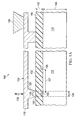
- FIGS. 1A-1C presents cross-sectional views of portions of example electronic pressure-sensing device 100 embodiments of the disclosure.
- the device 100 comprises a transistor 105 located on a semiconductor substrate 110.
- the device 100 also comprises a linker arm 115 that has a tip 120 which touches a contact region 125 of the substrate 110 near the transistor 105.
- the device 100 also comprises a pressure converter 130 that is mechanically coupled to the linker arm 115.
- the pressure converter 130 is configured to cause, in response to a pressure change, the tip 120 to impart a force capable of changing an electrical conductivity of the transistor 105.
- the contact region 125 of the substrate 110 is a portion of a side 132 of the substrate 110 that is contacted by the tip 120.
- the contact region 125 is considered to be near the transistor 105 when the transistor 105 is within a perimeter 134 of the contact region 125 and along an intended direction 136 of the force imparted from the tip 120.
- the tip 120 of the linker arm 115 is located over the substrate 110.
- situating the tip 120 over the substrate 110 can be conducive to optimizing the device's 100 sensitivity to pressure. For instance, consider when the substrate 110 includes a thin dielectric layer 140 on the transistor 105. E.g., a silicon oxide dielectric layer 140 having a thickness 142 of about 10 to 20 microns. Substantially all of the forces transmitted from the tip 120 reaches the transistor 105 because the thin dielectric layer 140 may not substantially dissipate the force from the tip 120.
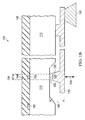
- the tip 120 of the linker arm 115 is located under the substrate 110.
- Such a configuration can provide the advantage of allowing ready access to the transistor 105.
- contacts 144 for connecting the transistor 105 to other devices can be located directly above the transistor 105 in the dielectric layer 140 thereby facilitating short interconnection pathways between the transistor 105 and the contacts 144.
- a device 100 configured such as shown in FIG. 1B may have less sensitivity than the configuration shown in FIG. 1A , because the substrate 110 can dissipate more of the force from the tip 120.
- relatively greater dissipation of the force can occur because the substrate 110 is substantially thicker (e.g., silicon thickness 146 of about 200 to 300 microns) than the dielectric layer 140.
- the substrate's thickness 114 can be reduced to decrease the dissipating effect and thereby increase pressure sensitivity. For instance, as shown in FIG. 1B , a portion of the substrate 110 directly under the transistor 105 can removed to provide a reduced substrate thickness 148 (e.g., about 50 to 100 microns) for the tip 120 to touch.
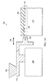
- the tip 120 of the linker arm 115 can be located adjacent to the substrate 110.
- Such embodiments can have the advantage of providing a device configuration that is more compact in the vertical dimension as compared to the configurations depicted in FIG. 1A or 1B .
- the linker arm 115 can be made of any solid material and have any shape that is conducive to transmitting the pressure changes registered by the pressure converter 130 to contact region 125.
- the linker arm 115 can be made of metal or plastic that can be molded, bent, machined or otherwise shaped to provide a body 150 that couples to the pressure converter 130 to the substrate 110, and, provide a tip 120 that can touch the contact region 125.
- the surface's 152 area needs to be balanced with the preference of having the surface 152 centered over the transistor 105, and large enough in area, so as to provide a reproducible amount of force to the transistor 105 for a same unit change in pressure.
- the desire for reproducibility is applicable within a single device and among different devices, e.g., manufactured in a batch process.
- the surface's 152 area ranges from 10 to 100 time large than the area occupied by the transistor 105 on the substrate 110. For instance, consider when the transistor 105 is manufactured at the 40 nm node (e.g., the transistor's 105 gate length is about 40 nm), and thereby occupies an area of about 0.02 microns 2 .
- the surface's 152 area preferably range from about 0.2 to 2 microns 2 . In other cases, however, larger transistors (e.g., 65 nm node and higher) having more reliable electrical characteristics, may be used. In such cases, a surface 152 area of greater than about 2 microns 2 may be desirable.
- the linker arms 115 it is preferable to configure the linker arms 115 to have a beveled tip 120. Such a configuration can help focus the force imparted from linker arm 115 onto the contact region 125.
- the substrate 100 can include a dielectric layer 140.
- the dielectric layer 140 can be part of an interconnect structure that includes metal interconnect lines, vias and contacts (not shown) that couple the transistor 105 to other components (not shown) of the device 100.
- the strained dielectric layer 140 can be configured to impart a tensile force or a compressive force to the transistor 105.
- the strained dielectric layer 140 includes one or more of layers composed of silicon nitride, silicon oxynitride, or silicon oxide.
- a strained dielectric layer 140 can change (i.e., increase or decrease) the electrical sensitivity of the transistor 105 with respect to the force imparted from the tip 120 of the linker arm 115.
- the transistor's 105 sensitivity can be assessed by measuring the change in the transistor's drain current for a given applied gate voltage and force imparted by the tip 120, as compared to an equivalent transistor with an unstrained dielectric layer.
- a strained dielectric layer 140 that applies a compressive force along direction 136 to an n-type metal oxide semiconductor (nMOS) transistor 105 can increase the transistor's 105 sensitivity.
- the conductivity of the nMOS transistor 105 changes to a greater extent in response to the force imparted from the tip 120, as compared to an equivalent nMOS transistor 105 covered by an unstrained dielectric layer 140 and receiving the same imparted force.
- a strained dielectric layer 140 applying a tensile force along direction 136 to an nMOS transistor 105 can decrease the transistor's 105 sensitivity. That is, the conductivity of the nMOS transistor 105 changes to a lesser extent in response to the force imparted from the tip 120, as compared to an equivalent nMOS transistor 105 covered by an unstrained dielectric layer 140 and receiving the same imparted force.
- a strained dielectric layer 140 that applies a compressive force along direction 136 to a p-type metal oxide semiconductor (pMOS) transistor 105 can decrease the transistor's 105 sensitivity. That is, the conductivity of the pMOS transistor 105 changes to a lesser extent in response to the force imparted from the tip 120, as compared to an equivalent pMOS transistor 105 covered by an unstrained dielectric layer 140 and receiving the same imparted force.
- a strained dielectric layer 140 that applies a tensile force along direction 135 to a pMOS transistor 105 can increase the transistor's 105 sensitivity.
- the conductivity of the pMOS transistor 105 changes to a greater extent in response to the force imparted from the tip 120, as compared to an equivalent pMOS transistor 105 covered by an unstrained dielectric layer 140 and receiving the same imparted force.
- a strained dielectric layer to increase the sensitivity of a transistor to externally applied forces is contrary to certain conventional integrated circuit (IC) designs, which often try to minimize the transistor's sensitivity to externally applied forces. Minimal sensitivity to external force is often sought, so as to avoid steps in the manufacture of the IC having undesired effects on the electrical properties of the transistors in the IC, and thereby causing lower yields of ICs that function within acceptable ranges.
- IC integrated circuit
- the device 100 can further include a reference transistor 155 located on the substrate 110.
- a separation distance 157 between the reference transistor 155 and the transistor 105 is sufficient that the force imparted from the tip 120 does not substantially change the electrical conductivity of the reference transistor 155.
- the transistor 105 and the reference transistor 155 are separated by a distance 157 that is at least about 5 times greater that the square-root of the area of the tip surface 152 that touches the contact region 125 of the substrate 110. For example when the area of the tip surface 152 equals about 2 microns 2 , the separation distance is about 10 microns.
- the reference transistor 155 can also be desirable for the reference transistor 155 to be situated such that it is outside of the perimeter 134 of the contact region 125 and not along the intended direction 136 of the force imparted from the tip 120.
- the reference transistor is not depicted because the direction 136 of the force from tip 120 travels laterally across the substrate 110 and therefore could affect a reference transistor 155 located within the cross-sectional depicted in the figure. Rather, it would be preferable for the reference transistor to be located either inside or outside of the cross-section depicted in FIG. 1C .
- the transistor 105 and the reference transistor 155 are both either pMOS transistors or nMOS transistors. This can facilitate having the electrical properties of the transistors 105, 155 well-matched to each other, which it turn, makes in easier to detect differences the electrical responses of the transistors 105, 155 when a force is applied from the tip 120.
- one of the transistors 105, 155 can be one of a pMOS or nMOS transistor, and the other transistor 155, 105 can be the other of an nMOS or pMOS transistor.
- one or both of the transistors 105, 155 can be a bipolar transistor or other type of transistor.
- the transistor 105 and the reference transistor 155 are both covered with a strained dielectric layer 140.
- the strained dielectric layer 140 is configured to impart one of a tensile force or a compressive force to the transistor 105 and the reference transistor 155.
- Such embodiments benefit from the lower expense and simpler process of depositing a single dielectric layer 140 on the transistors 105, 155. Additionally because they have the same dielectric layer 140 thereon, the transistors 105, 155 can have the same electrically properties, which can be useful when they are incorporated to certain types of differential amplifier circuit.
- suitable masking and deposition processes can be used to provide a only a strained dielectric layer on the transistor 105, and only an unstrained dielectric layer on the reference transistor 155. This can be beneficial when the force imparted from the tip 120 would otherwise have a substantial affect on the electrical properties of the reference transistor, e.g., even if the reference transistor 155 is remote from the contact region 123.
- the pressure converter 130 is attached to a same side 132 of substrate 110 that the tip 120 touches.
- the device 100 can be configured as an audio device, such as a microphone, a recording device, a telephone, or combination thereof, or a pressure transducer.
- the pressure converter 130 can be include, or be, a diaphragm that is attached to the body 150 of the linker arm 115, which in turn, is attached to the substrate 110. In other cases, however, the pressure converter 130 can be directly attached to the side 132 of the substrate 110.
- the diaphragm pressure converter 130 can be configured to move in response to a pressure change such that a mechanical force is imparted through the body 150 to the tip 120, thereby causing the tip 120 to impart a force, in direction 136, to the contact region 125.
- the diaphragm pressure converter 130 can mechanically vibrate in response to a sound wave traveling through a medium that the device 100 or the pressure converter 130 is in (e.g., air, liquid or solid), and, these mechanical vibrations can be imparted to the tip 120 of the linker arm 115.
- one or both of the linker arm 115 or the pressure converter 130 are not attached to the substrate 110.
- the pressure converter 130 and linker arm 115 can be separately attached to a second substrate 160 and situated adjacent to the substrate 110.
- the transistor 105 and reference transistor 155 are both part of a differential amplifier electrical circuit of the device 100.
- FIG. 2 presents an example differential amplifier electrical circuit 200 of an electronic pressure-sensing device of the disclosure, such as the devices 100 presented in FIGS. 1A-1C .
- the transistor 105 and reference transistor 155 can be coupled to a common voltage source 210 (e.g., by applying a voltage, V s ) via a common nodal point 215.
- V s voltage source electrodes 220, 222 of both transistors 105, 155
- An input current (I in ) is split between the transistors 105, 155.
- transistors 105, 155 When the transistors 105, 155 are electrically equal they each carry half of I in . When the force from the tip 120 ( FIG. 1 ) is applied to one transistor 105 but not the other transistor 155, then one of the transistors (e.g., either transistor 105 or reference transistor 155) will be more conductive and therefore carry more of the current. The difference in first and second currents (I1 out , I2 out ) being carried, in turn, will cause different first and second voltages (V1 out , V2 out ) on the drain electrodes 224, 226 of the transistors 105, 155.
- first and second currents I1 out , I2 out
- the circuit 200 can further include a third transistor 230.
- the third transistor 230 can be used to control the I in to the transistors 105, 155, e.g., by adjusting a voltage (V G ) applied to the gate 225 of the third transistor 220.
- the circuit 200 can also include resistors 235, 237 that are coupled to the drain electrodes 224, 226 of the transistors 105, 155. In other embodiments, additional transistors could be used, instead of or in addition to, the resistors 235, 237, to bear the current load.
- FIG. 3 presents a flow diagram of another embodiment of the disclosure, a method 300 of measuring pressure changes. Any of the embodiments of the device 100, such as discussed above in the context of FIGS. 1A-2 , can be used in performing the method 300.
- the method 300 comprises a step 310 of moving the linker arm 115 coupled to a pressure converter 130.
- the movement of the linker arm 115 in step 310 is in response to the pressure converter 130 being mechanically vibrated (step 320) by a pressure change in the medium surrounding the pressure converter.
- the movement of the linker arm 115 causes its tip 120 to exert a change in a force (step 330) imparted to the contact region 125 of the substrate 110.
- the method 300 also comprises a step 340 of applying a voltage V s across a transistor 105 located on the substrate 110 and near the contact region 125.
- the method 300 further comprises recording, in step 350, a first voltage (V1 out ) from the transistor 105 that varies as a function of changes in the imparted force.
- V1 out a first voltage
- I1 out a first current from the transistor 105 that varies as a function of changes in the imparted force.
- V G a selected gate voltage
- the I1 out can change (e.g., increase for an nMOS transistor 105) by about 15 percent or more when a force is applied from the tip 120 (e.g., about 1x10 -4 N or greater), as compared to when no force is applied.
- V G applied in step 350 is about 0.01 to 0.15 Volts, which can facilitate a change in I1 out of about 30 percent or more when the force from the tip 120 is applied.
- the method 300 further includes a step 360, of applying the same voltage (V s ) to the reference transistor 155 located on the substrate 110.
- the reference transistor 155 can have a common input node 215 with the transistor 105.
- a second voltage (V2 out ) from the reference transistor 155 does not substantially vary in response to changes in the imparted force from the tip 120. The presence of the reference transistor can facilitate the detection of changes in electrical response of the transistor 105.
- step 370 a difference in the voltages from the transistor 105 and the reference transistor 155 (e.g., V1 out -V2 out ) can be recorded, the voltage differential varying as a function of changes in the imparted force.
- an alternative circuit 200 FIG. 2
- I1 out -I2 out One skilled in the art would understand how to perform suitable steps to convert the recorded voltage or current, or, voltage or current differentials of steps 350 or 370, respectively, into stored information or otherwise useful information for an end-user.
- Still another embodiment of the disclosure is a method for manufacturing an electronic pressure-sensing device. Any of the embodiments of devices 100 discussed in the context of FIG. 1A-3 can be manufactured by the method.
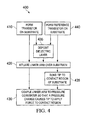
- FIG. 4 presents a flow diagram of an example method 400 of fabricating an electronic pressure-sensing device in accordance with the disclosure.
- the method 400 comprises a step 410 of forming a transistor 105 on a substrate 110.
- the method 400 also comprises a step 420 of situating a linker arm 115 over the substrate 110 such that the tip 120 of the linker arm 115 can touch a contact region 125 of the substrate 110, the contact region 125 being near the transistor 105.
- the method 400 further comprises a step 430 of coupling the linker arm 115 to a pressure converter 130 such that a pressure change in a medium surrounding the pressure converter 130 can cause the tip 120 to impart a force to the contact region 125.
- forming the transistor 105 on the substrate 110 in step 410 can include fabricating the transistor 105 in or on a semiconductor substrate 110, such as a silicon wafer substrate, using photolithographic patterning, dopant implantation, etching, and other conventional semiconductor processing techniques.
- a semiconductor substrate 110 such as a silicon wafer substrate
- photolithographic patterning, dopant implantation, etching, and other conventional semiconductor processing techniques One skilled in the art would be familiar with the processes to form, part of step 410, nMOS, pMOS or other transistor types.
- forming the transistor 105 on the substrate 110 in step 410 can include mounting a prefabricated IC that includes the transistor 105 to a printed circuit board substrate 110.
- forming the transistor 105 on the substrate 110 in step 410 can include a step 435 of depositing a dielectric layer 140 on the substrate 105 such that the transistor 105 is covered by the dielectric layer 140.
- the dielectric layer 140 deposited in step 435 is a strained dielectric layer.
- the strained dielectric layer 140 is configured to impart one of a tensile force or a compressive force to the transistor 105.
- One skilled in the art would be familiar with methods to deposit unstrained or strained dielectric layers 140, e.g., as part of a semiconductor transistor front-end fabrication process flow.
- a strained silicon nitride dielectric layer 140 can be deposited on a silicon substrate, such that one of a compressive force or a tensile force is applied to the transistor 105.
- the method 400 can further include a step 440 of forming a reference transistor 155 on the substrate 110.
- the reference transistor 155 is preferably formed at a location on the substrate 110 that is a sufficient distance 157 separated from the transistor 105 that the force to be imparted from the linker arm's 115 tip 120 would not substantially change the electrical conductivity of the reference transistor 155.
- the step 440 of forming the reference transistor 155 is part of the same semiconductor transistor front-end fabrication process flow used to form the transistor 105 in step 410.
- the dielectric layer 140 e.g., a strained dielectric layer
- step 435 can also cover the reference transistor 155.
- a separate dielectric layer (e.g., an unstrained dielectric layer) deposition step 445 can be performed to cover the reference transistor 155.
- forming the reference transistor 155 on the substrate 110 in step 440 can include mounting a prefabricated second IC, that includes the reference transistor 155, to the same printed circuit board substrate 110 that the transistor 105 (e.g., in an IC) is mounted to.
- the linker arm 115 and pressure converter 130 are prefabricated components that are situated and coupled, in accordance with steps 420 and 430, respectively.
- steps 420 and 430 respectively.
- one skilled in the art would be familiar with processes to mold, bend, or machine the linker arm 115 into the appropriate shape from metal, plastic or similar materials, and, with the procedures to manufacture pressure converters 130, such as diaphragms or other types of pressure-sensitive structures.
- the step 420 of situating the linker arm 120 over the substrate 110 can further include a step 450 of bonding the tip 120 to the contact region 125.
- the tip 120 can be bonded using adhesive materials such as epoxy or solder. Having the tip 120 bonded to the contact region 125 can help avoid propagating harmonic vibrations through the substrate 110. Harmonic vibrations might occur if the tip 120 were to hit the substrate 110 from a position separated from and above the substrate 110 as part of imparting the force. Such harmonic vibrations could interfere with the accurate conversion of the pressure changes received by the pressure converter 130 into changes in electrical conductivity in the transistor 105.
Landscapes
- Physics & Mathematics (AREA)
- General Physics & Mathematics (AREA)
- Pressure Sensors (AREA)
- Measuring Fluid Pressure (AREA)
- Electrostatic, Electromagnetic, Magneto- Strictive, And Variable-Resistance Transducers (AREA)
Applications Claiming Priority (1)
| Application Number | Priority Date | Filing Date | Title |
|---|---|---|---|
| US12/465,309 US8037771B2 (en) | 2009-05-13 | 2009-05-13 | Electronic pressure-sensing device |
Publications (2)
| Publication Number | Publication Date |
|---|---|
| EP2251663A2 true EP2251663A2 (fr) | 2010-11-17 |
| EP2251663A3 EP2251663A3 (fr) | 2014-03-05 |
Family
ID=42555617
Family Applications (1)
| Application Number | Title | Priority Date | Filing Date |
|---|---|---|---|
| EP10162776.8A Withdrawn EP2251663A3 (fr) | 2009-05-13 | 2010-05-13 | Dispositif de détection électronique de pression |
Country Status (6)
| Country | Link |
|---|---|
| US (1) | US8037771B2 (fr) |
| EP (1) | EP2251663A3 (fr) |
| JP (1) | JP5885909B2 (fr) |
| KR (1) | KR101512527B1 (fr) |
| CN (1) | CN101886962B (fr) |
| TW (1) | TWI424152B (fr) |
Cited By (1)
| Publication number | Priority date | Publication date | Assignee | Title |
|---|---|---|---|---|
| US20240049483A1 (en) * | 2020-09-03 | 2024-02-08 | The Regents Of The University Of California | Pressure sensor device with organic electrochemical transistors |
Families Citing this family (2)
| Publication number | Priority date | Publication date | Assignee | Title |
|---|---|---|---|---|
| TWI493402B (zh) * | 2013-03-01 | 2015-07-21 | Univ Chung Hua | 觸控面板及其製備方法 |
| KR102297773B1 (ko) | 2021-02-04 | 2021-09-06 | 주식회사 피앤씨랩스 | 발수성 및 공기 투과성이 향상된 일회용 흡수용품 |
Citations (1)
| Publication number | Priority date | Publication date | Assignee | Title |
|---|---|---|---|---|
| GB1122386A (en) * | 1964-12-16 | 1968-08-07 | Standard Telephones Cables Ltd | Improvements in or relating to electromechanical transducers |
Family Cites Families (22)
| Publication number | Priority date | Publication date | Assignee | Title |
|---|---|---|---|---|
| GB1049130A (en) * | 1964-03-12 | 1966-11-23 | Intermetall Ges Fur Metallurg | Improvements in pressure transducers and circuit arrangements therefor |
| US3566216A (en) * | 1968-08-07 | 1971-02-23 | Stow Lab Inc | An electromechanical transducer including a semiconductor and sensitivity controlling coupling means |
| JPS4829194B1 (fr) * | 1969-09-18 | 1973-09-07 | ||
| JPS5134696Y2 (fr) * | 1971-01-26 | 1976-08-27 | ||
| JPS61140182A (ja) * | 1984-12-12 | 1986-06-27 | Mitsubishi Electric Corp | 圧力センサ |
| JPS61154086A (ja) * | 1984-12-26 | 1986-07-12 | Fujitsu Ltd | 半導体温度センサ |
| JPS61153537A (ja) * | 1984-12-26 | 1986-07-12 | Fujitsu Ltd | 半導体圧力センサ |
| JPS61222178A (ja) * | 1985-03-15 | 1986-10-02 | Sharp Corp | 電界効果型圧力センサ |
| JP2822613B2 (ja) * | 1990-06-11 | 1998-11-11 | 株式会社デンソー | 半導体圧力センサ |
| JPH04105369A (ja) * | 1990-08-24 | 1992-04-07 | Honda Motor Co Ltd | 半導体センサ |
| US5155061A (en) * | 1991-06-03 | 1992-10-13 | Allied-Signal Inc. | Method for fabricating a silicon pressure sensor incorporating silicon-on-insulator structures |
| JP3365028B2 (ja) * | 1994-03-14 | 2003-01-08 | 株式会社デンソー | 圧力検出装置 |
| JP3053007B2 (ja) * | 1997-07-28 | 2000-06-19 | 日本電気株式会社 | 指紋センサ |
| US6550337B1 (en) * | 2000-01-19 | 2003-04-22 | Measurement Specialties, Inc. | Isolation technique for pressure sensing structure |
| GB0101241D0 (en) * | 2001-01-17 | 2001-02-28 | Walker Filtration Ltd | Electronic sensing device |
| US7434476B2 (en) * | 2003-05-07 | 2008-10-14 | Califronia Institute Of Technology | Metallic thin film piezoresistive transduction in micromechanical and nanomechanical devices and its application in self-sensing SPM probes |
| CN100449815C (zh) * | 2003-07-11 | 2009-01-07 | 友达光电股份有限公司 | 半导体压力传感器 |
| US7109055B2 (en) * | 2005-01-20 | 2006-09-19 | Freescale Semiconductor, Inc. | Methods and apparatus having wafer level chip scale package for sensing elements |
| US7442597B2 (en) * | 2005-02-02 | 2008-10-28 | Texas Instruments Incorporated | Systems and methods that selectively modify liner induced stress |
| CN100588911C (zh) * | 2007-05-10 | 2010-02-10 | 北方工业大学 | 一种灵敏大信号输出微型压力传感器 |
| TWI420086B (zh) * | 2008-10-15 | 2013-12-21 | Ind Tech Res Inst | 軟性電子壓力感測裝置及其製造方法 |
| JP4973718B2 (ja) * | 2009-01-27 | 2012-07-11 | セイコーエプソン株式会社 | 圧力検出ユニット、及び圧力センサー |
-
2009
- 2009-05-13 US US12/465,309 patent/US8037771B2/en not_active Expired - Fee Related
-
2010
- 2010-04-27 TW TW099113363A patent/TWI424152B/zh not_active IP Right Cessation
- 2010-05-07 KR KR20100042858A patent/KR101512527B1/ko not_active Expired - Fee Related
- 2010-05-12 JP JP2010109863A patent/JP5885909B2/ja not_active Expired - Fee Related
- 2010-05-12 CN CN201010178744.4A patent/CN101886962B/zh not_active Expired - Fee Related
- 2010-05-13 EP EP10162776.8A patent/EP2251663A3/fr not_active Withdrawn
Patent Citations (1)
| Publication number | Priority date | Publication date | Assignee | Title |
|---|---|---|---|---|
| GB1122386A (en) * | 1964-12-16 | 1968-08-07 | Standard Telephones Cables Ltd | Improvements in or relating to electromechanical transducers |
Cited By (2)
| Publication number | Priority date | Publication date | Assignee | Title |
|---|---|---|---|---|
| US20240049483A1 (en) * | 2020-09-03 | 2024-02-08 | The Regents Of The University Of California | Pressure sensor device with organic electrochemical transistors |
| US12364089B2 (en) * | 2020-09-03 | 2025-07-15 | The Regents Of The University Of California | Pressure sensor device with organic electrochemical transistors with microstructured hydrogel gating medium |
Also Published As
| Publication number | Publication date |
|---|---|
| TWI424152B (zh) | 2014-01-21 |
| KR101512527B1 (ko) | 2015-04-15 |
| KR20100122860A (ko) | 2010-11-23 |
| JP2010266441A (ja) | 2010-11-25 |
| US8037771B2 (en) | 2011-10-18 |
| EP2251663A3 (fr) | 2014-03-05 |
| CN101886962B (zh) | 2014-07-02 |
| CN101886962A (zh) | 2010-11-17 |
| TW201100769A (en) | 2011-01-01 |
| JP5885909B2 (ja) | 2016-03-16 |
| US20100288048A1 (en) | 2010-11-18 |
Similar Documents
| Publication | Publication Date | Title |
|---|---|---|
| US7563692B2 (en) | Microelectromechanical system pressure sensor and method for making and using | |
| US4906586A (en) | Suspended gate field effect semiconductor pressure transducer device | |
| US7448277B2 (en) | Capacitive pressure sensor and method therefor | |
| US7785912B2 (en) | Piezo-TFT cantilever MEMS fabrication | |
| US10276147B2 (en) | Microphone system and method for manufacturing the same | |
| US10155656B2 (en) | Inter-poly connection for parasitic capacitor and die size improvement | |
| CN104891423B (zh) | 不具有背板的双隔膜mems麦克风 | |
| WO2007117198A1 (fr) | Composant integre et son procede de fabrication | |
| US20240397828A1 (en) | Piezoelectric device having piezoelectric structure disposed between patterned conductive structures | |
| US8037771B2 (en) | Electronic pressure-sensing device | |
| JP7485045B2 (ja) | 圧力センサ構造、圧力センサ装置および圧力センサ構造の製造方法 | |
| US20100187646A1 (en) | Ultra low pressure sensor and method of fabrication of same | |
| US7615845B1 (en) | Active shielding of conductors in MEMS devices | |
| US20100167430A1 (en) | Apparatus and method for testing a transducer and/or electronic circuitry associated with a transducer | |
| US20090283846A1 (en) | Backside controlled mems capacitive sensor and interface and method | |
| KR102909338B1 (ko) | 전계효과 트랜지스터를 포함하는 마이크로폰 | |
| CN1838837B (zh) | 固体电容式结构微型传声器 | |
| JP2007208548A (ja) | 音響センサ | |
| CN121547714B (zh) | 一种指向性麦克风及其加工方法 | |
| US20250159423A1 (en) | Foundry-compatible process for a mems audio device | |
| JPH0711446B2 (ja) | 加速度センサ | |
| JPS6318272A (ja) | 圧電形加速度検出器 | |
| WO2024103263A1 (fr) | Capteur de pression, procédé de fabrication s'y rapportant et appareil électronique | |
| CN113933537A (zh) | 加速度传感器芯片及其制备方法 | |
| JPS6271282A (ja) | 触覚センサ及びその製造方法 |
Legal Events
| Date | Code | Title | Description |
|---|---|---|---|
| PUAI | Public reference made under article 153(3) epc to a published international application that has entered the european phase |
Free format text: ORIGINAL CODE: 0009012 |
|
| AK | Designated contracting states |
Kind code of ref document: A2 Designated state(s): AL AT BE BG CH CY CZ DE DK EE ES FI FR GB GR HR HU IE IS IT LI LT LU LV MC MK MT NL NO PL PT RO SE SI SK SM TR |
|
| AX | Request for extension of the european patent |
Extension state: BA ME RS |
|
| PUAL | Search report despatched |
Free format text: ORIGINAL CODE: 0009013 |
|
| AK | Designated contracting states |
Kind code of ref document: A3 Designated state(s): AL AT BE BG CH CY CZ DE DK EE ES FI FR GB GR HR HU IE IS IT LI LT LU LV MC MK MT NL NO PL PT RO SE SI SK SM TR |
|
| AX | Request for extension of the european patent |
Extension state: BA ME RS |
|
| RIC1 | Information provided on ipc code assigned before grant |
Ipc: H01L 29/84 20060101ALI20140129BHEP Ipc: G01L 9/00 20060101AFI20140129BHEP |
|
| 17P | Request for examination filed |
Effective date: 20140903 |
|
| RBV | Designated contracting states (corrected) |
Designated state(s): AL AT BE BG CH CY CZ DE DK EE ES FI FR GB GR HR HU IE IS IT LI LT LU LV MC MK MT NL NO PL PT RO SE SI SK SM TR |
|
| STAA | Information on the status of an ep patent application or granted ep patent |
Free format text: STATUS: EXAMINATION IS IN PROGRESS |
|
| 17Q | First examination report despatched |
Effective date: 20171106 |
|
| STAA | Information on the status of an ep patent application or granted ep patent |
Free format text: STATUS: THE APPLICATION IS DEEMED TO BE WITHDRAWN |
|
| 18D | Application deemed to be withdrawn |
Effective date: 20180317 |