EP2246905A2 - Photovoltaische Mehrfachübergangsstruktur mit dreidimensionaler Unterzelle und Verfahren dafür - Google Patents
Photovoltaische Mehrfachübergangsstruktur mit dreidimensionaler Unterzelle und Verfahren dafür Download PDFInfo
- Publication number
- EP2246905A2 EP2246905A2 EP10161069A EP10161069A EP2246905A2 EP 2246905 A2 EP2246905 A2 EP 2246905A2 EP 10161069 A EP10161069 A EP 10161069A EP 10161069 A EP10161069 A EP 10161069A EP 2246905 A2 EP2246905 A2 EP 2246905A2
- Authority
- EP
- European Patent Office
- Prior art keywords
- subcell
- layer
- junction
- type
- elongated structures
- Prior art date
- Legal status (The legal status is an assumption and is not a legal conclusion. Google has not performed a legal analysis and makes no representation as to the accuracy of the status listed.)
- Withdrawn
Links
- 238000000034 method Methods 0.000 title claims description 34
- 239000000758 substrate Substances 0.000 claims description 49
- 229910021417 amorphous silicon Inorganic materials 0.000 claims description 23
- 238000000151 deposition Methods 0.000 claims description 12
- 229910021419 crystalline silicon Inorganic materials 0.000 claims description 8
- 239000000463 material Substances 0.000 description 31
- 229910021424 microcrystalline silicon Inorganic materials 0.000 description 20
- 238000009792 diffusion process Methods 0.000 description 10
- 239000010408 film Substances 0.000 description 10
- 239000004065 semiconductor Substances 0.000 description 10
- 238000005229 chemical vapour deposition Methods 0.000 description 9
- 238000010521 absorption reaction Methods 0.000 description 8
- 238000012546 transfer Methods 0.000 description 8
- 229910000530 Gallium indium arsenide Inorganic materials 0.000 description 7
- 230000008901 benefit Effects 0.000 description 7
- IJGRMHOSHXDMSA-UHFFFAOYSA-N Atomic nitrogen Chemical compound N#N IJGRMHOSHXDMSA-UHFFFAOYSA-N 0.000 description 6
- 238000013459 approach Methods 0.000 description 6
- 238000005530 etching Methods 0.000 description 6
- 239000000203 mixture Substances 0.000 description 6
- 238000005516 engineering process Methods 0.000 description 5
- 238000000605 extraction Methods 0.000 description 5
- GNPVGFCGXDBREM-UHFFFAOYSA-N germanium atom Chemical compound [Ge] GNPVGFCGXDBREM-UHFFFAOYSA-N 0.000 description 5
- 229910052757 nitrogen Inorganic materials 0.000 description 5
- 238000004544 sputter deposition Methods 0.000 description 5
- XUIMIQQOPSSXEZ-UHFFFAOYSA-N Silicon Chemical compound [Si] XUIMIQQOPSSXEZ-UHFFFAOYSA-N 0.000 description 4
- 239000000654 additive Substances 0.000 description 4
- 230000000996 additive effect Effects 0.000 description 4
- 229910052732 germanium Inorganic materials 0.000 description 4
- 229910052738 indium Inorganic materials 0.000 description 4
- 229910052710 silicon Inorganic materials 0.000 description 4
- 239000010703 silicon Substances 0.000 description 4
- 238000000927 vapour-phase epitaxy Methods 0.000 description 4
- 229910052785 arsenic Inorganic materials 0.000 description 3
- 230000008021 deposition Effects 0.000 description 3
- 230000031700 light absorption Effects 0.000 description 3
- 238000001451 molecular beam epitaxy Methods 0.000 description 3
- 238000012545 processing Methods 0.000 description 3
- RQNWIZPPADIBDY-UHFFFAOYSA-N arsenic atom Chemical compound [As] RQNWIZPPADIBDY-UHFFFAOYSA-N 0.000 description 2
- 238000000231 atomic layer deposition Methods 0.000 description 2
- 229910052790 beryllium Inorganic materials 0.000 description 2
- ATBAMAFKBVZNFJ-UHFFFAOYSA-N beryllium atom Chemical compound [Be] ATBAMAFKBVZNFJ-UHFFFAOYSA-N 0.000 description 2
- 239000000969 carrier Substances 0.000 description 2
- 238000004871 chemical beam epitaxy Methods 0.000 description 2
- 239000004020 conductor Substances 0.000 description 2
- 239000002019 doping agent Substances 0.000 description 2
- 238000001312 dry etching Methods 0.000 description 2
- APFVFJFRJDLVQX-UHFFFAOYSA-N indium atom Chemical compound [In] APFVFJFRJDLVQX-UHFFFAOYSA-N 0.000 description 2
- 238000007641 inkjet printing Methods 0.000 description 2
- 239000012212 insulator Substances 0.000 description 2
- 229910052751 metal Inorganic materials 0.000 description 2
- 239000002184 metal Substances 0.000 description 2
- 229910044991 metal oxide Inorganic materials 0.000 description 2
- 150000004706 metal oxides Chemical class 0.000 description 2
- 238000004088 simulation Methods 0.000 description 2
- 238000001228 spectrum Methods 0.000 description 2
- 238000004528 spin coating Methods 0.000 description 2
- 238000002207 thermal evaporation Methods 0.000 description 2
- GYHNNYVSQQEPJS-UHFFFAOYSA-N Gallium Chemical compound [Ga] GYHNNYVSQQEPJS-UHFFFAOYSA-N 0.000 description 1
- BLRPTPMANUNPDV-UHFFFAOYSA-N Silane Chemical compound [SiH4] BLRPTPMANUNPDV-UHFFFAOYSA-N 0.000 description 1
- 229910000577 Silicon-germanium Inorganic materials 0.000 description 1
- INQLNSVYIFCUML-QZTLEVGFSA-N [[(2r,3s,4r,5r)-5-(6-aminopurin-9-yl)-3,4-dihydroxyoxolan-2-yl]methoxy-hydroxyphosphoryl] [(2r,3s,4r,5r)-5-(4-carbamoyl-1,3-thiazol-2-yl)-3,4-dihydroxyoxolan-2-yl]methyl hydrogen phosphate Chemical compound NC(=O)C1=CSC([C@H]2[C@@H]([C@H](O)[C@@H](COP(O)(=O)OP(O)(=O)OC[C@@H]3[C@H]([C@@H](O)[C@@H](O3)N3C4=NC=NC(N)=C4N=C3)O)O2)O)=N1 INQLNSVYIFCUML-QZTLEVGFSA-N 0.000 description 1
- 238000000862 absorption spectrum Methods 0.000 description 1
- 230000005540 biological transmission Effects 0.000 description 1
- 230000015572 biosynthetic process Effects 0.000 description 1
- 230000015556 catabolic process Effects 0.000 description 1
- 238000006243 chemical reaction Methods 0.000 description 1
- 150000001875 compounds Chemical class 0.000 description 1
- 238000010276 construction Methods 0.000 description 1
- 239000013078 crystal Substances 0.000 description 1
- 238000006731 degradation reaction Methods 0.000 description 1
- 238000005137 deposition process Methods 0.000 description 1
- 238000013461 design Methods 0.000 description 1
- 238000011161 development Methods 0.000 description 1
- 230000000694 effects Effects 0.000 description 1
- 238000004070 electrodeposition Methods 0.000 description 1
- 229910052733 gallium Inorganic materials 0.000 description 1
- 239000007789 gas Substances 0.000 description 1
- QUZPNFFHZPRKJD-UHFFFAOYSA-N germane Chemical compound [GeH4] QUZPNFFHZPRKJD-UHFFFAOYSA-N 0.000 description 1
- 229910052986 germanium hydride Inorganic materials 0.000 description 1
- 239000011521 glass Substances 0.000 description 1
- BHEPBYXIRTUNPN-UHFFFAOYSA-N hydridophosphorus(.) (triplet) Chemical compound [PH] BHEPBYXIRTUNPN-UHFFFAOYSA-N 0.000 description 1
- 239000012535 impurity Substances 0.000 description 1
- 238000004519 manufacturing process Methods 0.000 description 1
- 150000002739 metals Chemical class 0.000 description 1
- 230000006911 nucleation Effects 0.000 description 1
- 238000010899 nucleation Methods 0.000 description 1
- 230000003287 optical effect Effects 0.000 description 1
- 238000001020 plasma etching Methods 0.000 description 1
- 229920000642 polymer Polymers 0.000 description 1
- 230000000644 propagated effect Effects 0.000 description 1
- 239000007787 solid Substances 0.000 description 1
- 238000000992 sputter etching Methods 0.000 description 1
- 239000010409 thin film Substances 0.000 description 1
- 238000003631 wet chemical etching Methods 0.000 description 1
Images






Classifications
-
- H—ELECTRICITY
- H10—SEMICONDUCTOR DEVICES; ELECTRIC SOLID-STATE DEVICES NOT OTHERWISE PROVIDED FOR
- H10F—INORGANIC SEMICONDUCTOR DEVICES SENSITIVE TO INFRARED RADIATION, LIGHT, ELECTROMAGNETIC RADIATION OF SHORTER WAVELENGTH OR CORPUSCULAR RADIATION
- H10F77/00—Constructional details of devices covered by this subclass
- H10F77/10—Semiconductor bodies
- H10F77/14—Shape of semiconductor bodies; Shapes, relative sizes or dispositions of semiconductor regions within semiconductor bodies
- H10F77/148—Shapes of potential barriers
-
- H—ELECTRICITY
- H10—SEMICONDUCTOR DEVICES; ELECTRIC SOLID-STATE DEVICES NOT OTHERWISE PROVIDED FOR
- H10F—INORGANIC SEMICONDUCTOR DEVICES SENSITIVE TO INFRARED RADIATION, LIGHT, ELECTROMAGNETIC RADIATION OF SHORTER WAVELENGTH OR CORPUSCULAR RADIATION
- H10F10/00—Individual photovoltaic cells, e.g. solar cells
- H10F10/10—Individual photovoltaic cells, e.g. solar cells having potential barriers
- H10F10/16—Photovoltaic cells having only PN heterojunction potential barriers
- H10F10/161—Photovoltaic cells having only PN heterojunction potential barriers comprising multiple PN heterojunctions, e.g. tandem cells
-
- H—ELECTRICITY
- H10—SEMICONDUCTOR DEVICES; ELECTRIC SOLID-STATE DEVICES NOT OTHERWISE PROVIDED FOR
- H10F—INORGANIC SEMICONDUCTOR DEVICES SENSITIVE TO INFRARED RADIATION, LIGHT, ELECTROMAGNETIC RADIATION OF SHORTER WAVELENGTH OR CORPUSCULAR RADIATION
- H10F10/00—Individual photovoltaic cells, e.g. solar cells
- H10F10/10—Individual photovoltaic cells, e.g. solar cells having potential barriers
- H10F10/17—Photovoltaic cells having only PIN junction potential barriers
- H10F10/172—Photovoltaic cells having only PIN junction potential barriers comprising multiple PIN junctions, e.g. tandem cells
-
- H—ELECTRICITY
- H10—SEMICONDUCTOR DEVICES; ELECTRIC SOLID-STATE DEVICES NOT OTHERWISE PROVIDED FOR
- H10F—INORGANIC SEMICONDUCTOR DEVICES SENSITIVE TO INFRARED RADIATION, LIGHT, ELECTROMAGNETIC RADIATION OF SHORTER WAVELENGTH OR CORPUSCULAR RADIATION
- H10F77/00—Constructional details of devices covered by this subclass
- H10F77/10—Semiconductor bodies
- H10F77/16—Material structures, e.g. crystalline structures, film structures or crystal plane orientations
- H10F77/162—Non-monocrystalline materials, e.g. semiconductor particles embedded in insulating materials
- H10F77/164—Polycrystalline semiconductors
- H10F77/1642—Polycrystalline semiconductors including only Group IV materials
- H10F77/1645—Polycrystalline semiconductors including only Group IV materials including microcrystalline silicon
-
- H—ELECTRICITY
- H10—SEMICONDUCTOR DEVICES; ELECTRIC SOLID-STATE DEVICES NOT OTHERWISE PROVIDED FOR
- H10F—INORGANIC SEMICONDUCTOR DEVICES SENSITIVE TO INFRARED RADIATION, LIGHT, ELECTROMAGNETIC RADIATION OF SHORTER WAVELENGTH OR CORPUSCULAR RADIATION
- H10F77/00—Constructional details of devices covered by this subclass
- H10F77/10—Semiconductor bodies
- H10F77/16—Material structures, e.g. crystalline structures, film structures or crystal plane orientations
- H10F77/162—Non-monocrystalline materials, e.g. semiconductor particles embedded in insulating materials
- H10F77/166—Amorphous semiconductors
- H10F77/1662—Amorphous semiconductors including only Group IV materials
-
- Y—GENERAL TAGGING OF NEW TECHNOLOGICAL DEVELOPMENTS; GENERAL TAGGING OF CROSS-SECTIONAL TECHNOLOGIES SPANNING OVER SEVERAL SECTIONS OF THE IPC; TECHNICAL SUBJECTS COVERED BY FORMER USPC CROSS-REFERENCE ART COLLECTIONS [XRACs] AND DIGESTS
- Y02—TECHNOLOGIES OR APPLICATIONS FOR MITIGATION OR ADAPTATION AGAINST CLIMATE CHANGE
- Y02E—REDUCTION OF GREENHOUSE GAS [GHG] EMISSIONS, RELATED TO ENERGY GENERATION, TRANSMISSION OR DISTRIBUTION
- Y02E10/00—Energy generation through renewable energy sources
- Y02E10/50—Photovoltaic [PV] energy
- Y02E10/544—Solar cells from Group III-V materials
-
- Y—GENERAL TAGGING OF NEW TECHNOLOGICAL DEVELOPMENTS; GENERAL TAGGING OF CROSS-SECTIONAL TECHNOLOGIES SPANNING OVER SEVERAL SECTIONS OF THE IPC; TECHNICAL SUBJECTS COVERED BY FORMER USPC CROSS-REFERENCE ART COLLECTIONS [XRACs] AND DIGESTS
- Y02—TECHNOLOGIES OR APPLICATIONS FOR MITIGATION OR ADAPTATION AGAINST CLIMATE CHANGE
- Y02E—REDUCTION OF GREENHOUSE GAS [GHG] EMISSIONS, RELATED TO ENERGY GENERATION, TRANSMISSION OR DISTRIBUTION
- Y02E10/00—Energy generation through renewable energy sources
- Y02E10/50—Photovoltaic [PV] energy
- Y02E10/545—Microcrystalline silicon PV cells
-
- Y—GENERAL TAGGING OF NEW TECHNOLOGICAL DEVELOPMENTS; GENERAL TAGGING OF CROSS-SECTIONAL TECHNOLOGIES SPANNING OVER SEVERAL SECTIONS OF THE IPC; TECHNICAL SUBJECTS COVERED BY FORMER USPC CROSS-REFERENCE ART COLLECTIONS [XRACs] AND DIGESTS
- Y02—TECHNOLOGIES OR APPLICATIONS FOR MITIGATION OR ADAPTATION AGAINST CLIMATE CHANGE
- Y02E—REDUCTION OF GREENHOUSE GAS [GHG] EMISSIONS, RELATED TO ENERGY GENERATION, TRANSMISSION OR DISTRIBUTION
- Y02E10/00—Energy generation through renewable energy sources
- Y02E10/50—Photovoltaic [PV] energy
- Y02E10/547—Monocrystalline silicon PV cells
-
- Y—GENERAL TAGGING OF NEW TECHNOLOGICAL DEVELOPMENTS; GENERAL TAGGING OF CROSS-SECTIONAL TECHNOLOGIES SPANNING OVER SEVERAL SECTIONS OF THE IPC; TECHNICAL SUBJECTS COVERED BY FORMER USPC CROSS-REFERENCE ART COLLECTIONS [XRACs] AND DIGESTS
- Y02—TECHNOLOGIES OR APPLICATIONS FOR MITIGATION OR ADAPTATION AGAINST CLIMATE CHANGE
- Y02E—REDUCTION OF GREENHOUSE GAS [GHG] EMISSIONS, RELATED TO ENERGY GENERATION, TRANSMISSION OR DISTRIBUTION
- Y02E10/00—Energy generation through renewable energy sources
- Y02E10/50—Photovoltaic [PV] energy
- Y02E10/548—Amorphous silicon PV cells
Definitions
- This invention relates to multijunction photovoltaic devices and a method for forming a multijunction photovoltaic structure.
- Solar cells are classified as either single junction or multijunction solar cells according to their structure.
- a single junction solar cell only absorbs light from the region of the spectrum with photon energy greater than its single band gap. The efficiency is limited by transmission and thermalisation losses in the solar cell. If an incident photon has less energy than the band gap of the semiconductor material, the photon cannot be absorbed since there is not enough energy to excite an electron from the conduction band to the valence band. If an incident photon has more energy than the band gap the excess energy will be converted into heat.
- Multijunction solar cells also known as tandem solar cells
- Two technological approaches have been investigated over the years. Firstly a mechanically stacked approach where solar cells with different band gap energies are fabricated on their individual substrates and then brought together such that the solar cell consists of a stack of subcells. This allows subcell materials to have different lattice constants. However, separate substrates are required for each subcell and complicated processing is required for the mechanical stacking procedure.
- the monolithic approach where different materials are all grown on a single substrate and connected in series by interband tunnel diodes.
- the various materials need to be lattice matched to the substrate. Only one substrate is needed which is a cost advantage compared with the mechanically stacked approach and while the growth of the monolithic solar cell structure may be more complicated for III-V materials, the processing is simpler and cheaper than the mechanically stacked approach.
- the output current of the monolithic multijunction solar cell is limited to the smallest of the currents produced by any of the individual subcells. Ideally the same current is generated in each of the subcells i.e. the subcells are 'current matched.' This will result in a higher efficiency from the whole photovoltaic device.
- Microcrystalline silicon hereafter referred to as ⁇ c-Si
- ⁇ c-Si has a band gap of 1.1eV, compared with the 1.7eV band gap of amorphous silicon (hereafter referred to as a-Si). Therefore ⁇ c-Si is suitable for use as the bottom subcell of a multijunction solar cell with a-Si as the top subcell.
- a-Si amorphous silicon
- ⁇ c-Si as the narrow band gap cell instead of the alternative of amorphous SiGe (a-SiGe) are (1) the higher quantum efficiency in the long-wavelength region, (2) negligible light induced degradation, (3) reduced materials cost, since ⁇ c-Si can be made using SiH4, which is a relatively low cost gas compared to GeH4, and (4) ⁇ c-Si cells can be made with a high fill factor.
- ⁇ c-Si cells require much thicker i-layers (several ⁇ m thick) to absorb the sunlight; this is an effect of the lower interband absorption coefficients in indirect band gap crystals compared to amorphous semiconductors.
- ⁇ c-Si cells require much thicker i-layers (several ⁇ m thick) to absorb the sunlight; this is an effect of the lower interband absorption coefficients in indirect band gap crystals compared to amorphous semiconductors.
- the most efficient commercial multijunction solar cell is a monolithic triple junction device with subcells consisting of Ga 0.5 In 0.5 P, Ga 0.99 In 0.01 As and Ge.
- the Ge subcell in this device usually absorbs about the same number of photons as the GaInP and GaInAs layers combined.
- a higher efficiency would be achieved if a 1eV material were added between the GaInAs and Ge subcells as this would result in closer current matching for all of the subcells and a higher overall cell efficiency.
- this 1eV material In order to be incorporated into a monolithic device this 1eV material also needs to be lattice matched to germanium.
- GaInNAs is one example of a material which can fulfil these requirements. There is a significant bowing of the GaInAs band gap when introducing small amounts of nitrogen.
- Figure 1 represents a range of In and N compositions, for which lattice matching (squares) occurs and for which the samples have a fundamental band gap of 1eV (circles). The desired 1eV band gap can be achieved by using several different compositions, which are plotted as circles in Figure 1 .
- lattice matching conditions to GaAs (which is very close to that of germanium, and is a possible alternative substrate) are shown as squares in Figure 1 . At the composition where both curves intersect, the lattice matching condition as well as the 1eV band gap requirement is fulfilled.
- This material has a composition of 8% indium and 2.8% nitrogen [ K Volz et al, J. Cryst. Growth 248, 451 (2003 )] .
- a multijunction photovoltaic structure includes a first subcell including a p-n or p-i-n junction with elongated structures, wherein the elongated structure is a structure that has a height larger than at least one of a length and a width, and a second subcell, arranged in tandem with the first subcell, and including a planar p-n or p-i-n junction.
- the elongated structure is a structure that has a height (Y) being larger than at least one of its other two dimensions (i.e., width) (X2), and its height (Y), width (X2), and a pitch (X1) follow the following relationship: Y>X2 and X1>X2.
- a pitch (X1) of the elongated structures of the first subcell is between 10nm and 10 ⁇ m.
- a width (X2) of the elongated structures of the first subcell is between 10nm and 10 ⁇ m.
- a height (Y) of the elongated structures of the first subcell is between 10nm and 10 ⁇ m.
- the p-n junction with elongated structures of the first subcell comprise a p-type or n-type layer with three-dimensional structures formed therein, and the other of the p-type or n-type layer deposited on top thereof.
- the other of the p-type or n-type layer is planarized.
- the p-i-n junction with elongated structures of the first subcell include a p-type or n-type layer with three-dimensional structures formed therein, an intrinsic layer deposited on top thereof, and the other of the p-type or n-type layer formed on top of the intrinsic layer.
- the first subcell and the second subcell have different band gap energies and the elongated structures improve current matching between the first subcell and the second subcell.
- the first subcell is one of a ⁇ c-Si subcell and an a-Si subcell
- the second subcell is the other of a ⁇ c-Si subcell and an a-Si subcell.
- the first subcell is an GaInNAs subcell.
- the multijunction photovoltaic structure further includes a tunnel junction separating the first subcell and the second subcell.
- the multijunction photovoltaic structure further includes at least one additional subcell in tandem with the first subcell, said additional subcell having either a p-n or p-i-n junction with elongated structures, or a planar p-n or p-i-n junction.
- the at least one additional subcell comprises a p-n or p-i-n junction with elongated structures.
- the at least one additional subcell comprises a planar p-n or p-i-n junction.
- the elongated structures comprise at least one of ribs or pillars.
- a method for forming a multijunction photovoltaic structure includes forming a first subcell including a p-n or p-i-n junction with elongated structures, wherein the elongated structure is a structure that has a height larger than at least one of a length and a width, and forming a second subcell, arranged in tandem with the first subcell, and including a planar p-n or p-i-n junction.
- the method includes forming a p-type or n-type layer of the first subcell including the p-n junction with three-dimensional structures therein, depositing the other of the p-type or n-type layer thereon.
- the method includes forming a p-type or n-type layer of the first subcell including the p-i-n junction with three-dimensional structures therein, depositing an intrinsic layer thereon, and forming the other of the p-type or n-type layer on top of the intrinsic layer.
- the method includes forming the elongated structures of the first subcell by depositing the respective layers of the p-n or p-i-n junction conformally on top of a substrate or underlying layer having three-dimensional structures corresponding to the elongated structures.
- the method includes forming at least one additional subcell in tandem having either a p-n or p-i-n junction with elongated structures, or a planar p-n or p-i-n junction.
- the first subcell is one of a ⁇ c-Si subcell and an a-Si subcell
- the second subcell is the other of a ⁇ c-Si subcell and an a-Si subcell.
- the first subcell is GaInNAs subcell.
- the elongated structures include at least one of ribs or pillars.
- a planar layer or surface is defined such that any feature in a layer or surface has an aspect ratio lower than one, i.e. the dimensions of a feature in the plane of the substrate are larger than the dimension of the feature perpendicular to the substrate.
- the layer or surface is considered to contain elongated structures (i.e. is 3D structured) if at least one dimension of a feature in the plane of the substrate (i.e., a length or width) is less than the dimension of the feature perpendicular to the plane of the substrate (i.e., height).
- an elongated structure may take the form of pillars (in which both dimensions in the plane of the substrate are less than the dimension of the feature perpendicular to the substrate) or fins (in which only one dimension in the plane of the substrate is less than the dimension of the feature perpendicular to the substrate).
- pillars in which both dimensions in the plane of the substrate are less than the dimension of the feature perpendicular to the substrate
- fins in which only one dimension in the plane of the substrate is less than the dimension of the feature perpendicular to the substrate.
- Various other forms of elongate structures also are possible, and are well within the scope of the invention.
- the present invention discloses the use of a p-n or p-i-n junction with elongated structures in a subcell of a multijunction photovoltaic structure with at least one other planar subcell deposited on top of the 3D structured subcell.
- a construction is particularly suited for fabrication using the processing techniques described in commonly assigned, co-pending UK patent application 0813568.3 , which describes methods of growing solar cell films conformally on a nanostructured surface of a substrate.
- FIG. 1 shows a simplified, schematic version of solar cells to illustrate the key features of the present invention.
- Other layers that are typically used in photovoltaic devices, which are omitted here for clarity, may also be included in the structures provided to enable the optimum use of the present invention. These layers may include but are not limited to: further subcells, nucleation layers, buffer layers, back surface field layers, tunnel junctions, window layers and contact layers.
- the present invention is described with the formation of the solar cell layers on an n-doped substrate. It would be equally possible to apply the present invention to a device formed on a p-doped substrate, by reversing the order of the p-doped and n-doped layers in each subcell.
- An object of the present invention is to enable a gain in the efficiency of multijunction photovoltaic devices by decoupling the requirements based on the necessary absorption depth and the possible minority carrier diffusion length in the material of a subcell; and/or to provide a structure that is quicker and easier to fabricate compared with present technology.
- the present invention enables a photovoltaic device fabricated in any suitable material system with the presence of a p-n junction or p-i-n junction forming elongated structures in at least one subcell, with at least one planar subcell in tandem with the subcell containing elongated structures.
- the photovoltaic device may be fabricated by any suitable method; this includes but is not limited to molecular beam epitaxy, chemical beam epitaxy, vapour phase epitaxy, chemical vapour deposition, spin coating, ink-jet printing, stamp-based transfers, device bonding and transfer of the desired structures out of solution.
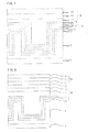
- Figures 2 thru 8 illustrate exemplary structures of subcells in a multijunction solar cell according to the present invention.
- the subcells include one or more three-dimensional (3D) subcells in stacked arrangement.
- Figure 2 shows that a first layer 2, which is doped n-type, may be formed on a planar substrate 1.
- the first layer 2 may consist of elongated structures. These elongated structures may be formed directly on the substrate 1 using a mask, self-organization, a seeded substrate, or any other suitable method. Alternatively, a planar layer may be deposited and the elongated structures formed by any suitable etching technique to form the first layer 2. These elongated structures may or may not be connected to each other by a layer of the same material at the interface to the substrate. As shown in Figure 2 a p-type layer 4 may be deposited on the elongated structures such that the surface of the p-type layer 4 is planar.
- an intrinsic layer may be deposited between the n-type layer 2 and the p-type layer 4.
- an intrinsic layer 3 may be deposited conformally on the n-type layer 2 as shown in Figure 3 .
- the intrinsic layer 3 may be deposited such that the surface is planar as shown in Figure 4 .
- the intrinsic layer 3 may be omitted.
- Layers 2, 3 (if present), and 4 together form a first subcell A of the photovoltaic device.
- a tunnel junction layer 5 may be deposited on the uppermost layer 4 of the first subcell A.
- a planar n-type layer 6 may be deposited on the tunnel junction layer 5.
- a planar intrinsic layer 7 may be deposited on the n-type layer 6. Alternatively the intrinsic layer 7 may be omitted.
- a planar p-type layer 8 may be deposited on the n-type layer 6 or the intrinsic layer 7 if present. Layers 6, 7 (if present), and 8 form a second subcell B of the photovoltaic device. Further subcells consisting of p-n or p-i-n junctions containing either elongated structures or planar layers may be deposited on top of the second subcell B. Further subcells consisting of p-n or p-i-n junctions may be deposited on the substrate prior to the deposition of layer 2. In this case layer 2 will be deposited on the uppermost layer of a subcell instead of the substrate. The substrate may also have been treated to form a further subcell in the photovoltaic structure. Each subcell will be separated by an appropriate tunnel junction.
- the substrate surface of a photovoltaic device may consist of a first layer 2 having the elongated structures.
- These elongated structures 2 may be formed directly on a substrate using a mask, self-organization, a seeded substrate, or any other suitable method.
- the elongated structures may be formed by any suitable etching technique. If the first layer 2 serving as the substrate has been formed to act as an additional subcell then the elongated structures will form part of the p-type uppermost layer of the first layer 2, with an n-type region 9 below as shown in Figure 5 .
- a buffer layer 10 may be deposited conformally on the surface of the substrate. Alternatively the buffer layer 10 may be omitted.
- a tunnel junction layer 5 may be deposited conformally on the buffer layer 10 (if present) or the substrate layer 2.
- a first n-type layer 11 of a subcell A may be deposited conformally on the tunnel junction layer 5.
- a second p-type layer 12 of a subcell A may be deposited on the n-type layer 11 such that the surface of the p-type layer 12 is planar.
- the p-type layer 12 may be deposited conformally on the n-type layer 11.
- a tunnel junction layer 13 may be deposited conformally on the p-type layer 12, and a first n-type layer 14 of a subcell B may be deposited on the tunnel junction layer 13 such that the surface of the n-type layer 14 is planar as shown in Figure 6 .
- a planar tunnel junction layer 13 and first n-type layer 14 may be formed on the planar surface of the p-type layer 12.
- an intrinsic layer 15 may be deposited on the n-type layer 14 or may be omitted.
- a planar p-type layer 16 of the subcell B may be deposited on the n-type layer 14 or the intrinsic layer 15 (if present).
- Further p-n or p-i-n junctions may be deposited conformally between the last layer of subcell A and the first layer of subcell B to form a plurality of p-n junctions with an elongated structure.
- Further subcells consisting of p-n or p-i-n junctions may be deposited on the subcell B, these additional subcells may be planar, or may contain elongated structures.
- the structure may contain an intrinsic layer 17 between the n-type layer 11 and the p-type layer 12.
- the intrinsic layer 17 may be deposited conformally, in which case the p-type layer 12 may be deposited conformally or such that the surface is planar.
- the intrinsic layer 17 may be deposited such that the surface is planar, and the p-type layer 12 and subcell B will then be deposited as planar layers.
- the preferred pitch X1 of the elongated structures in layer 2 or the other layers as describe herein is between 10nm and 10mm depending on the carrier diffusion length in the material being used and the thicknesses of the layers that are deposited conformally on the elongated structures.
- the preferred width X2 of the elongated structures is between 10nm and 10mm depending on the carrier diffusion length of the material being used.
- the preferred height Y of the elongated structures is between 10nm and 10mm depending on the absorption coefficient of the material being used, where Y>X2 to satisfy the condition that the structure is an elongated structure, and X1>X2 to avoid merging of neighbouring elongated structures.
- the elongated structures of the first layer 2 may be connected to each other by a planar layer of the same material as the elongated structures, such that the planar layer is in contact with the layer below 1, as shown in Figure 10 .
- the elongated structures of the first layer 2 may not be connected to each other by a layer of the same material, as shown in Figure 11 .
- the photovoltaic device structure consists of an elongated structured subcell with one or more additional planar subcells, where the structured subcell is the one closest to the substrate, and at least one planar subcell is on top of the structured one.
- the structured subcell contains a set of elongated structures such as fins or a set of pillars, and such a set of fins or pillars has substantially uniform pitch and height.
- the fins or pillars are made of a conductor, or a semiconductor, or an insulator.
- Each individual subcell including the structured one contains a p-n/p-i-n junction, which consists of a p-doped semiconductor, an optional non-doped semiconductor and an n-doped semiconductor.
- a-Si/ ⁇ c-Si tandem cell an amorphous silicon/microcrystalline silicon (hereafter referred to as a-Si/ ⁇ c-Si) tandem cell, but the design is not limited to this material combination.
- the preferred pitch X1 of the fins or pillars is within the range of 500nm to 5 ⁇ m, while the preferred height Y of the fins or pillars is in the range of 1 ⁇ m to 10 ⁇ m.
- Configuration 1 as shown in Figure 12 , has a 3D structured ⁇ c-Si subcell and a planar a-Si subcell.
- the ⁇ c-Si structured sub-cell is directly formed on the substrate and an additional a-Si sub-cell is created on top of the ⁇ c-Si. Incident light enters the structure on the side furthest from the substrate.
- Configuration 2 as shown in Figure 13 , has a 3D structured a-Si subcell and a planar ⁇ c-Si subcell.
- the a-Si sub-cell is 3D structured and is the sub-cell closest to the substrate.
- a ⁇ c-Si subcell is created on top of the a-Si subcell.
- Incident light enters the structure from the substrate side.
- Such application of present invention will potentially improve the conventional a-Si/uc-Si thin film technology.
- ⁇ c-Si cells require much thicker i-layers to absorb the sunlight due to its lower absorption coefficients.
- the key idea of present invention is to decouple the carrier diffusion path to the light absorption depth; hence a thicker ⁇ c-Si cell can be used without affecting the carrier extraction coefficient.
- a-Si/ ⁇ c-Si tandem cell Another problem when fabricating a a-Si/ ⁇ c-Si tandem cell is the variation of film thickness across a large substrate during the CVD deposition process.
- the thickness of each subcell affects the amount of the light it absorbs and hence the photo-generated current. Therefore, the thickness variation in a film is a disadvantage for achieving good current matching between adjacent subcells for the entire device, as the excess current generated in the thicker subcells cannot be extracted and is lost as heat. This reduces the overall efficiency of a photovoltaic device.
- the thickness of the structured subcell is mainly controlled by the height of the initial vertical structures rather than the thickness of the film deposited around these vertical structures. Therefore, the film uniformity will be improved provided the height of the vertical structures is larger than the thickness of the film and the vertical structures have a substantially uniform height.
- a a-Si/ ⁇ c-Si tandem cell is usually fabricated via chemical vapour deposition (CVD) technology, therefore by providing a substrate which has a set of substantially vertical structures, such a structured a-Si/ ⁇ c-Si tandem cell can be obtained through subsequent substantially conformal CVD deposition.
- CVD chemical vapour deposition
- the set of fins or pillars are part of the substrate, and the subsequent doped Si/non-doped Si/doped Si layers coated around these fins or pillars form a three-dimensional junction.
- any tandem/multi-junction photovoltaic devices current matching between adjacent subcells is important.
- the performance of each subcell will set an upper-limit for the maximum possible current that can be extracted from other subcells, and hence can limit the output current of whole photovoltaic devices.
- a major advantage of having such a structured subcell is that the performance of a potentially poorer subcell can be enhanced due to these three-dimensional junctions, which decouples the light absorption depth and carrier extraction length. Longer light absorption depth can now be achieved while keeping the carrier extraction length short, therefore improving the overall current generation of a photovoltaic device.
- Adjacent subcells may have different band gap energies and the elongated structures improve current matching between the first subcell and the second subcell.
- the vertical or elongated structures on the substrate can be formed by either additive or subtractive method, where the additive and subtractive methods may be defined as following.
- Additive e.g. deposition, transfer
- Transfer methods include dry transfer methods such as stamp-based transfers, and device bonding as well as wet transfer methods where the transfer of the desired structures occurs out of solution.
- Subtractive e.g. etching, sputtering, and dissolving
- Sputtering includes ion milling.
- the vertical or elongated structures on the substrate will have the same material composition as the substrate if they are formed via subtractive method, or they can be made of insulator (glass, polymers), conductor (conducting metal oxides, metals) or semiconductor (doped or non-doped Si) if they are formed via additive method.
- the pitch of the elongated structures is preferred to be within the range of 100nm to 1 ⁇ m.
- the height of the elongated structures may be less than 5 ⁇ m, and is preferred to be less than 2 ⁇ m.
- the pitch of the elongated structures may be less than 10 ⁇ m, and is preferred to be less than 5 ⁇ m.
- the height of the elongated structures may be less than 20 ⁇ m, and is preferred to be less than 10 ⁇ m.
- the vertical or elongated structures can be a set of 1D pillars or 2D ribs and their smallest dimension is preferred to be less than 100nm.
- a conducting layer metal or conducting metal oxides
- the sequential plurality of films coated around these elongated structures can be deposited via methods such as chemical vapour deposition (CVD), molecular beam epitaxy (MBE), Vapour Phase Epitaxy (VPE), Atomic Layer Deposition (ALD), sputtering, electro-deposition, thermal evaporation etc.
- CVD chemical vapour deposition
- MBE molecular beam epitaxy
- VPE Vapour Phase Epitaxy
- ALD Atomic Layer Deposition
- sputtering electro-deposition
- the overall thickness of these films which forms the first sub-cell is required to completely fill the gaps between neighbouring vertical structures.
- the second sub-cell which is a planar one is then formed on top of the first structured sub-cell by further depositing a plurality of films that give the p-n/p-i-n junctions.
- a photovoltaic cell consisting of subcells of 0.7eV Ge (D), 1eV GaInNAs (A), 1.4eV InGaAs (B) and 1.9eV GaInP (C), contains elongated structures in the GaInNAs subcell (A) as described in the present invention.
- a planar buffer layer 40 may be deposited on the uppermost layer 41 of the Ge subcell D.
- a planar tunnel junction layer (not shown) may be deposited on the buffer layer.
- a layer 42 of elongated structures of n-type GaInNAs may be formed on the tunnel junction layer.
- the elongated structures may be formed directly on the substrate 1 using a mask, self-organization, a seeded substrate, or any other suitable method as described above.
- a planar layer may be deposited and the elongated structures formed by any suitable etching technique as described above.
- the elongated structures are formed by etching.
- the elongated structures may be annealed under an arsenic overpressure to improve the material quality.
- a layer of p-type GaInNAs 43 may be deposited on the elongated structures of layer 42 such that the surface of the layer is substantially planar.
- the remaining planar subcells (B and C) and appropriate tunnel junctions may be deposited on the GaInNAs subcell A.
- the elongated structures have substantially uniform pitch, height and width. Due to low mobility of the carriers and short carrier lifetimes, the carrier diffusion length in GaInNAs is too short, resulting in the GaInNAs subcell A not providing sufficient current to match the current produced in the other subcells (D, B and C) and therefore limiting the efficiency of the photovoltaic device.
- the absorption depth of a subcell is controlled by the height of the elongated structures (Y). Increasing Y increases the current produced in the GaInNAs subcell A.
- the low carrier diffusion length in GaInNAs only restricts the appropriate values of the width X2 and the pitch X1 of the elongated structures and these can be optimized separately from the height y.
- the height of the elongated structures is preferably in the range 0.5mm to 5mm, the width of the elongated structures is preferably in the range 50nm to 500nm and the pitch of the elongated structures is preferably in the range 500nm to 5mm.
- a photovoltaic cell consists of subcells of 0.7eV Ge (D), 1eV GaInNAs (A), 1.4eV InGaAs (B) and 1.9eV GaInP (C).
- the n-type layer 50 of the Ge subcell D is planar, and the p-type layer 51 of the Ge subcell contains elongated structures.
- the elongated structures have substantially uniform pitch, height and width.
- the height Y of the elongated structures is preferably in the range 0.5mm to 5mm
- the width X2 of the elongated structures is preferably in the range 50nm to 500nm
- the pitch X1 of the elongated structures is preferably in the range 500nm to 5mm.
- a buffer layer 52 may be deposited conformally on the Ge subcell p-type layer 51, or the buffer layer may be omitted.
- a tunnel junction layer 53 may be deposited conformally on the buffer layer 52 or the p-type Ge layer 51.
- a GaInNAs n-type layer 54 may be deposited conformally on the tunnel junction layer 53.
- a GaInNAs p-type layer 57 may be deposited on the GaInNAs n-type layer 54, and p-type layer 57 may be planarized such that the surface of the layer 57 is substantially planar.
- the remaining planar subcells (B and C) and appropriate tunnel junctions (e.g., 55 and 56 may be deposited on the GaInNAs subcell (2).
- this structure allows the height Y of the elongated structures to be optimized for the absorption depth independently from the parameters (the pitch X1 and the width X2) that depend of the carrier diffusion length in the material.
- This structure has the additional advantages of forming the elongated structures in the Ge substrate rather than the more difficult GaInNAs material and also benefits from improved carrier extraction due to the carriers travelling more of the distance in the high quality p-type Ge layer 51 rather than the lower quality n-type GaInNAs layer 54.
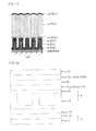
- FIG. 15 a simplified structure of the GaInNAs subcell A as described in this fourth embodiment ( Figure 15 ) was simulated and compared with a planar GaInNAs subcell.
- the unit cell used for the planar cell is shown in Figure 16 ; the unit cell used for the subcell A containing elongated structures is shown in Figure 17 .
- the software used was sentaurus TCAD v 2008.09.
- the cell was modeled as a 2D structure and was illuminated with an AM1.5G spectrum between 750-1300nm (to simulate the light that would pass through the higher bandgap 1.4eV InGaAs (B) and 1.9eV GaInP (C) subcells), the light was propagated through the cell using ray-tracing.
- planar cell ( Figure 16 ) had a 0.9mm planar layer of n-type GaInNAs deposited on planar p-type germanium Ge, and a 0.9mm planar layer of p-type GaInNAs deposited on the n-type GaInNAs.
- the photovoltaic devices are preferably grown by molecular beam epitaxy using silicon as the n-type dopant and beryllium as the p-type dopant.
- Solid sources are preferably used for the gallium, indium, silicon and beryllium, cracker cells for the arsenic and phosphorous, and an RF plasma source for the nitrogen.
- the GaInNAs layers are preferably grown in the temperature range 400-550°C
- the InGaAs layers are preferably grown in the temperature range 600-750°C
- the GaInP layers are preferably grown in the range 500-600°C.
- Other growth methods may also be used; this includes but is not limited to, chemical vapour deposition, vapour phase epitaxy and chemical beam epitaxy.
- the method can also include at least one additional subcell (second subcell) in tandem with the first subcell having either a p-n or p-i-n junction with elongated structures, or a planar p-n or p-I-n junction.
- the first subcell can be one of a ⁇ c-Si subcell and an a-Si subcell, and the second subcell can be the other of a ⁇ c-Si subcell and an a-Si subcell.
- the first subcell can also be a GaInNAs subcell and the elongated structures can comprise of at least one of ribs or pillars.
- the present invention enables a gain in the efficiency of multijunction photovoltaic devices by decoupling the requirements based on the necessary absorption depth and the possible minority carrier diffusion length in the material of a subcell; and/or to provide a structure that is quicker and easier to fabricate compared with present technology.
Landscapes
- Photovoltaic Devices (AREA)
Applications Claiming Priority (1)
| Application Number | Priority Date | Filing Date | Title |
|---|---|---|---|
| US12/430,308 US20100269895A1 (en) | 2009-04-27 | 2009-04-27 | Multijunction photovoltaic structure with three-dimensional subcell |
Publications (2)
| Publication Number | Publication Date |
|---|---|
| EP2246905A2 true EP2246905A2 (de) | 2010-11-03 |
| EP2246905A3 EP2246905A3 (de) | 2013-09-11 |
Family
ID=42575246
Family Applications (1)
| Application Number | Title | Priority Date | Filing Date |
|---|---|---|---|
| EP10161069.9A Withdrawn EP2246905A3 (de) | 2009-04-27 | 2010-04-26 | Photovoltaische Mehrfachübergangsstruktur mit dreidimensionaler Unterzelle und Verfahren dafür |
Country Status (3)
| Country | Link |
|---|---|
| US (1) | US20100269895A1 (de) |
| EP (1) | EP2246905A3 (de) |
| JP (1) | JP5038459B2 (de) |
Families Citing this family (6)
| Publication number | Priority date | Publication date | Assignee | Title |
|---|---|---|---|---|
| US8536445B2 (en) | 2006-06-02 | 2013-09-17 | Emcore Solar Power, Inc. | Inverted metamorphic multijunction solar cells |
| US20100206367A1 (en) * | 2009-02-18 | 2010-08-19 | Korea Institute Of Industrial Technology | Method for fabricating silicon nano wire, solar cell including silicon nano wire and method for fabricating solar cell |
| ITMI20111559A1 (it) * | 2011-08-30 | 2013-03-01 | St Microelectronics Srl | Strato tco di contatto frontale di un pannello solare a film sottile con strato barriera di metallo refrattario e processo di fabbricazione |
| US10872988B1 (en) | 2013-02-03 | 2020-12-22 | Mark R. Schroeder | Photovoltaic device |
| US11538949B2 (en) | 2013-02-03 | 2022-12-27 | Mark R. Schroeder | Sensor comprising a photovoltaic device |
| CN106688109A (zh) * | 2015-06-25 | 2017-05-17 | 华为技术有限公司 | 一种光电探测器 |
Citations (3)
| Publication number | Priority date | Publication date | Assignee | Title |
|---|---|---|---|---|
| GB813568A (en) | 1954-05-10 | 1959-05-21 | Roland Nicolas Payen | Improvements in aircraft |
| US4272641A (en) | 1979-04-19 | 1981-06-09 | Rca Corporation | Tandem junction amorphous silicon solar cells |
| US20070151595A1 (en) | 2005-12-30 | 2007-07-05 | Chih-Hung Chiou | Solar cell with superlattice structure and fabricating method thereof |
Family Cites Families (14)
| Publication number | Priority date | Publication date | Assignee | Title |
|---|---|---|---|---|
| JPS6451671A (en) * | 1987-08-24 | 1989-02-27 | Canon Kk | Solar cell |
| US5094697A (en) * | 1989-06-16 | 1992-03-10 | Canon Kabushiki Kaisha | Photovoltaic device and method for producing the same |
| JP2692964B2 (ja) * | 1989-07-14 | 1997-12-17 | 三洋電機株式会社 | 太陽電池 |
| JPH03151672A (ja) * | 1989-11-08 | 1991-06-27 | Sharp Corp | 非晶質シリコン太陽電池 |
| JPH04296060A (ja) * | 1991-03-26 | 1992-10-20 | Hitachi Ltd | 太陽電池 |
| JP3695950B2 (ja) * | 1998-07-31 | 2005-09-14 | 三洋電機株式会社 | 光電変換素子の製造方法 |
| US7605327B2 (en) * | 2003-05-21 | 2009-10-20 | Nanosolar, Inc. | Photovoltaic devices fabricated from nanostructured template |
| JP5324222B2 (ja) * | 2005-08-22 | 2013-10-23 | キュー・ワン・ナノシステムズ・インコーポレイテッド | ナノ構造およびそれを実施する光起電力セル |
| US9105776B2 (en) * | 2006-05-15 | 2015-08-11 | Stion Corporation | Method and structure for thin film photovoltaic materials using semiconductor materials |
| JP2007324324A (ja) * | 2006-05-31 | 2007-12-13 | Sumitomo Electric Ind Ltd | 太陽電池 |
| JP2008028118A (ja) * | 2006-07-20 | 2008-02-07 | Honda Motor Co Ltd | 多接合型太陽電池の製造方法 |
| US7629532B2 (en) * | 2006-12-29 | 2009-12-08 | Sundiode, Inc. | Solar cell having active region with nanostructures having energy wells |
| US7977568B2 (en) * | 2007-01-11 | 2011-07-12 | General Electric Company | Multilayered film-nanowire composite, bifacial, and tandem solar cells |
| EP2115782A1 (de) * | 2007-01-30 | 2009-11-11 | Solasta, Inc. | Photovoltaische zelle und verfahren zu ihrer herstellung |
-
2009
- 2009-04-27 US US12/430,308 patent/US20100269895A1/en not_active Abandoned
-
2010
- 2010-04-16 JP JP2010095287A patent/JP5038459B2/ja not_active Expired - Fee Related
- 2010-04-26 EP EP10161069.9A patent/EP2246905A3/de not_active Withdrawn
Patent Citations (3)
| Publication number | Priority date | Publication date | Assignee | Title |
|---|---|---|---|---|
| GB813568A (en) | 1954-05-10 | 1959-05-21 | Roland Nicolas Payen | Improvements in aircraft |
| US4272641A (en) | 1979-04-19 | 1981-06-09 | Rca Corporation | Tandem junction amorphous silicon solar cells |
| US20070151595A1 (en) | 2005-12-30 | 2007-07-05 | Chih-Hung Chiou | Solar cell with superlattice structure and fabricating method thereof |
Non-Patent Citations (4)
| Title |
|---|
| D. J. FRIEDMAN ET AL., J. CRYST. GROWTH, vol. 195, 1998, pages 409 |
| G. LEIBIGER ET AL., J. APPL. PHYS., vol. 90, no. 12, 2001, pages 5951 |
| K VOLZ ET AL., J. CRYST. GROWTH, vol. 248, 2003, pages 451 |
| M. MEUSEL ET AL.: "European roadmap for the development of III-V multi junction space solar cells", 19TH EUROPEAN PHOTOVOLTAIC SOLAR ENERGY CONFERENCE, 2004 |
Also Published As
| Publication number | Publication date |
|---|---|
| JP5038459B2 (ja) | 2012-10-03 |
| EP2246905A3 (de) | 2013-09-11 |
| US20100269895A1 (en) | 2010-10-28 |
| JP2010258449A (ja) | 2010-11-11 |
Similar Documents
| Publication | Publication Date | Title |
|---|---|---|
| Yamaguchi et al. | Multi-junction solar cells paving the way for super high-efficiency | |
| EP2745329B1 (de) | Pv-element | |
| KR102710224B1 (ko) | 전하-캐리어-선택적 접촉을 통해 연결되는 복수의 흡수체들을 구비한 태양 전지 | |
| CN203351629U (zh) | 光伏电池和光伏系统 | |
| US9716201B2 (en) | Silicon heterojunction photovoltaic device with wide band gap emitter | |
| US20090314337A1 (en) | Photovoltaic devices | |
| EP2168167A2 (de) | Auf nanodrähten basierende solarzellenstruktur | |
| WO2005020334A9 (en) | High efficiency tandem solar cells on silicon substrates using ultra thin germanium buffer layers | |
| US20140196773A1 (en) | Multi-junction iii-v solar cell | |
| EP2246905A2 (de) | Photovoltaische Mehrfachübergangsstruktur mit dreidimensionaler Unterzelle und Verfahren dafür | |
| US20080163924A1 (en) | Multijunction solar cell | |
| US10141461B2 (en) | Textured multi-junction solar cell and fabrication method | |
| US20100037940A1 (en) | Stacked solar cell | |
| US20110278537A1 (en) | Semiconductor epitaxial structures and semiconductor optoelectronic devices comprising the same | |
| CN114171615A (zh) | 一种硅基多结太阳电池及其渐变缓冲层 | |
| CN110911510A (zh) | 一种含超晶格结构的硅基氮化物五结太阳电池 | |
| Salama | Quantum Dot Solar cells | |
| Mizuno et al. | A “smart stack” triple-junction cell consisting of ingap/gaas and crystalline si | |
| KR101395028B1 (ko) | 탠덤형 태양전지 및 그의 제조 방법 | |
| KR101772432B1 (ko) | 다중밴드 Si-Ge 박막 단결정을 이용한 태양전지 및 그의 효율 개선방법 | |
| JP2006073833A (ja) | 太陽電池セルおよびその製造方法 | |
| Ringel et al. | Photovoltaic devices | |
| CN102386252A (zh) | 多接面光电池元件 | |
| HK1231253A (en) | Nanowire-based solar cell structure | |
| HK1231253A1 (en) | Nanowire-based solar cell structure |
Legal Events
| Date | Code | Title | Description |
|---|---|---|---|
| PUAI | Public reference made under article 153(3) epc to a published international application that has entered the european phase |
Free format text: ORIGINAL CODE: 0009012 |
|
| AK | Designated contracting states |
Kind code of ref document: A2 Designated state(s): AT BE BG CH CY CZ DE DK EE ES FI FR GB GR HR HU IE IS IT LI LT LU LV MC MK MT NL NO PL PT RO SE SI SK SM TR |
|
| AX | Request for extension of the european patent |
Extension state: AL BA ME RS |
|
| PUAL | Search report despatched |
Free format text: ORIGINAL CODE: 0009013 |
|
| AK | Designated contracting states |
Kind code of ref document: A3 Designated state(s): AT BE BG CH CY CZ DE DK EE ES FI FR GB GR HR HU IE IS IT LI LT LU LV MC MK MT NL NO PL PT RO SE SI SK SM TR |
|
| AX | Request for extension of the european patent |
Extension state: AL BA ME RS |
|
| RIC1 | Information provided on ipc code assigned before grant |
Ipc: H01L 31/0352 20060101ALI20130805BHEP Ipc: H01L 31/068 20120101AFI20130805BHEP |
|
| STAA | Information on the status of an ep patent application or granted ep patent |
Free format text: STATUS: THE APPLICATION IS DEEMED TO BE WITHDRAWN |
|
| 18D | Application deemed to be withdrawn |
Effective date: 20140312 |