EP2240970B1 - Perylen-halbleiter und methoden zu deren herstellung - Google Patents
Perylen-halbleiter und methoden zu deren herstellung Download PDFInfo
- Publication number
- EP2240970B1 EP2240970B1 EP09709379.3A EP09709379A EP2240970B1 EP 2240970 B1 EP2240970 B1 EP 2240970B1 EP 09709379 A EP09709379 A EP 09709379A EP 2240970 B1 EP2240970 B1 EP 2240970B1
- Authority
- EP
- European Patent Office
- Prior art keywords
- compounds
- compound
- group
- article
- present teachings
- Prior art date
- Legal status (The legal status is an assumption and is not a legal conclusion. Google has not performed a legal analysis and makes no representation as to the accuracy of the status listed.)
- Active
Links
- 239000004065 semiconductor Substances 0.000 title claims description 50
- 238000000034 method Methods 0.000 title claims description 42
- 238000002360 preparation method Methods 0.000 title description 24
- 125000002080 perylenyl group Chemical group C1(=CC=C2C=CC=C3C4=CC=CC5=CC=CC(C1=C23)=C45)* 0.000 title description 3
- CSHWQDPOILHKBI-UHFFFAOYSA-N peryrene Natural products C1=CC(C2=CC=CC=3C2=C2C=CC=3)=C3C2=CC=CC3=C1 CSHWQDPOILHKBI-UHFFFAOYSA-N 0.000 title 1
- 150000001875 compounds Chemical class 0.000 claims description 97
- 239000010409 thin film Substances 0.000 claims description 23
- 238000004519 manufacturing process Methods 0.000 claims description 16
- 125000004169 (C1-C6) alkyl group Chemical group 0.000 claims description 14
- 230000005669 field effect Effects 0.000 claims description 13
- 125000001997 phenyl group Chemical group [H]C1=C([H])C([H])=C(*)C([H])=C1[H] 0.000 claims description 9
- 125000000171 (C1-C6) haloalkyl group Chemical group 0.000 claims description 8
- 125000004400 (C1-C12) alkyl group Chemical group 0.000 claims description 7
- 229910052736 halogen Inorganic materials 0.000 claims description 7
- 150000002367 halogens Chemical class 0.000 claims description 7
- 230000003287 optical effect Effects 0.000 claims description 7
- 125000004641 (C1-C12) haloalkyl group Chemical group 0.000 claims description 6
- 150000001412 amines Chemical class 0.000 claims description 6
- 239000000010 aprotic solvent Substances 0.000 claims description 6
- LMBFAGIMSUYTBN-MPZNNTNKSA-N teixobactin Chemical compound C([C@H](C(=O)N[C@@H]([C@@H](C)CC)C(=O)N[C@@H](CO)C(=O)N[C@H](CCC(N)=O)C(=O)N[C@H]([C@@H](C)CC)C(=O)N[C@@H]([C@@H](C)CC)C(=O)N[C@@H](CO)C(=O)N[C@H]1C(N[C@@H](C)C(=O)N[C@@H](C[C@@H]2NC(=N)NC2)C(=O)N[C@H](C(=O)O[C@H]1C)[C@@H](C)CC)=O)NC)C1=CC=CC=C1 LMBFAGIMSUYTBN-MPZNNTNKSA-N 0.000 claims description 5
- 230000000295 complement effect Effects 0.000 claims description 4
- 229910052794 bromium Inorganic materials 0.000 claims description 3
- 125000006575 electron-withdrawing group Chemical group 0.000 claims description 3
- 230000005693 optoelectronics Effects 0.000 claims description 3
- XFXPMWWXUTWYJX-UHFFFAOYSA-N Cyanide Chemical compound N#[C-] XFXPMWWXUTWYJX-UHFFFAOYSA-N 0.000 claims description 2
- 229910052739 hydrogen Inorganic materials 0.000 claims description 2
- 239000000203 mixture Substances 0.000 description 43
- OKKJLVBELUTLKV-UHFFFAOYSA-N Methanol Chemical compound OC OKKJLVBELUTLKV-UHFFFAOYSA-N 0.000 description 42
- HEDRZPFGACZZDS-UHFFFAOYSA-N Chloroform Chemical compound ClC(Cl)Cl HEDRZPFGACZZDS-UHFFFAOYSA-N 0.000 description 32
- 239000007787 solid Substances 0.000 description 30
- 239000000463 material Substances 0.000 description 28
- 229910052757 nitrogen Inorganic materials 0.000 description 26
- ZMXDDKWLCZADIW-UHFFFAOYSA-N N,N-Dimethylformamide Chemical compound CN(C)C=O ZMXDDKWLCZADIW-UHFFFAOYSA-N 0.000 description 24
- WLLGXSLBOPFWQV-UHFFFAOYSA-N MGK 264 Chemical compound C1=CC2CC1C1C2C(=O)N(CC(CC)CCCC)C1=O WLLGXSLBOPFWQV-UHFFFAOYSA-N 0.000 description 22
- 239000002904 solvent Substances 0.000 description 20
- 238000007639 printing Methods 0.000 description 18
- 239000010410 layer Substances 0.000 description 16
- 238000004440 column chromatography Methods 0.000 description 15
- 125000002496 methyl group Chemical group [H]C([H])([H])* 0.000 description 15
- IJGRMHOSHXDMSA-UHFFFAOYSA-N Atomic nitrogen Chemical compound N#N IJGRMHOSHXDMSA-UHFFFAOYSA-N 0.000 description 14
- 238000006243 chemical reaction Methods 0.000 description 14
- 238000000921 elemental analysis Methods 0.000 description 14
- 230000037230 mobility Effects 0.000 description 14
- -1 cyano-substituted perylene Chemical group 0.000 description 13
- 125000001495 ethyl group Chemical group [H]C([H])([H])C([H])([H])* 0.000 description 13
- 239000000758 substrate Substances 0.000 description 13
- HEDRZPFGACZZDS-MICDWDOJSA-N Trichloro(2H)methane Chemical compound [2H]C(Cl)(Cl)Cl HEDRZPFGACZZDS-MICDWDOJSA-N 0.000 description 12
- 238000001816 cooling Methods 0.000 description 12
- 230000008569 process Effects 0.000 description 12
- 239000003480 eluent Substances 0.000 description 11
- 238000001914 filtration Methods 0.000 description 11
- 125000000217 alkyl group Chemical group 0.000 description 10
- 239000010408 film Substances 0.000 description 10
- 239000000047 product Substances 0.000 description 10
- VYPSYNLAJGMNEJ-UHFFFAOYSA-N Silicium dioxide Chemical compound O=[Si]=O VYPSYNLAJGMNEJ-UHFFFAOYSA-N 0.000 description 9
- 239000002244 precipitate Substances 0.000 description 9
- YFNKIDBQEZZDLK-UHFFFAOYSA-N triglyme Chemical compound COCCOCCOCCOC YFNKIDBQEZZDLK-UHFFFAOYSA-N 0.000 description 9
- WYURNTSHIVDZCO-UHFFFAOYSA-N Tetrahydrofuran Chemical compound C1CCOC1 WYURNTSHIVDZCO-UHFFFAOYSA-N 0.000 description 8
- 238000004528 spin coating Methods 0.000 description 8
- 238000005266 casting Methods 0.000 description 7
- 239000002131 composite material Substances 0.000 description 7
- DOBRDRYODQBAMW-UHFFFAOYSA-N copper(i) cyanide Chemical compound [Cu+].N#[C-] DOBRDRYODQBAMW-UHFFFAOYSA-N 0.000 description 7
- 239000003960 organic solvent Substances 0.000 description 7
- 238000005160 1H NMR spectroscopy Methods 0.000 description 6
- 230000008901 benefit Effects 0.000 description 6
- 239000003990 capacitor Substances 0.000 description 6
- 239000003795 chemical substances by application Substances 0.000 description 6
- 125000004093 cyano group Chemical group *C#N 0.000 description 6
- 238000000151 deposition Methods 0.000 description 6
- XBDQKXXYIPTUBI-UHFFFAOYSA-N dimethylselenoniopropionate Natural products CCC(O)=O XBDQKXXYIPTUBI-UHFFFAOYSA-N 0.000 description 6
- 125000001188 haloalkyl group Chemical group 0.000 description 6
- 125000001449 isopropyl group Chemical group [H]C([H])([H])C([H])(*)C([H])([H])[H] 0.000 description 6
- 238000012546 transfer Methods 0.000 description 6
- RTZKZFJDLAIYFH-UHFFFAOYSA-N Diethyl ether Chemical compound CCOCC RTZKZFJDLAIYFH-UHFFFAOYSA-N 0.000 description 5
- 239000008186 active pharmaceutical agent Substances 0.000 description 5
- 125000004432 carbon atom Chemical group C* 0.000 description 5
- 125000005843 halogen group Chemical group 0.000 description 5
- 239000003049 inorganic solvent Substances 0.000 description 5
- 229910001867 inorganic solvent Inorganic materials 0.000 description 5
- 150000002500 ions Chemical class 0.000 description 5
- 125000000959 isobutyl group Chemical group [H]C([H])([H])C([H])(C([H])([H])[H])C([H])([H])* 0.000 description 5
- 238000005259 measurement Methods 0.000 description 5
- 229920000642 polymer Polymers 0.000 description 5
- 238000007740 vapor deposition Methods 0.000 description 5
- 239000002518 antifoaming agent Substances 0.000 description 4
- 239000011230 binding agent Substances 0.000 description 4
- 125000000484 butyl group Chemical group [H]C([*])([H])C([H])([H])C([H])([H])C([H])([H])[H] 0.000 description 4
- 239000011248 coating agent Substances 0.000 description 4
- 238000000576 coating method Methods 0.000 description 4
- 229910052681 coesite Inorganic materials 0.000 description 4
- 238000002508 contact lithography Methods 0.000 description 4
- 229910052906 cristobalite Inorganic materials 0.000 description 4
- 239000002270 dispersing agent Substances 0.000 description 4
- 238000007646 gravure printing Methods 0.000 description 4
- 238000007641 inkjet printing Methods 0.000 description 4
- 239000007788 liquid Substances 0.000 description 4
- 229910052751 metal Inorganic materials 0.000 description 4
- 239000002184 metal Substances 0.000 description 4
- 238000000813 microcontact printing Methods 0.000 description 4
- 238000007645 offset printing Methods 0.000 description 4
- 238000013086 organic photovoltaic Methods 0.000 description 4
- 238000007649 pad printing Methods 0.000 description 4
- 125000001436 propyl group Chemical group [H]C([*])([H])C([H])([H])C([H])([H])[H] 0.000 description 4
- 238000007650 screen-printing Methods 0.000 description 4
- 239000000377 silicon dioxide Substances 0.000 description 4
- 229910052682 stishovite Inorganic materials 0.000 description 4
- YLQBMQCUIZJEEH-UHFFFAOYSA-N tetrahydrofuran Natural products C=1C=COC=1 YLQBMQCUIZJEEH-UHFFFAOYSA-N 0.000 description 4
- 229910052905 tridymite Inorganic materials 0.000 description 4
- ZWEHNKRNPOVVGH-UHFFFAOYSA-N 2-Butanone Chemical compound CCC(C)=O ZWEHNKRNPOVVGH-UHFFFAOYSA-N 0.000 description 3
- WEVYAHXRMPXWCK-UHFFFAOYSA-N Acetonitrile Chemical compound CC#N WEVYAHXRMPXWCK-UHFFFAOYSA-N 0.000 description 3
- UHOVQNZJYSORNB-UHFFFAOYSA-N Benzene Chemical compound C1=CC=CC=C1 UHOVQNZJYSORNB-UHFFFAOYSA-N 0.000 description 3
- YMWUJEATGCHHMB-UHFFFAOYSA-N Dichloromethane Chemical compound ClCCl YMWUJEATGCHHMB-UHFFFAOYSA-N 0.000 description 3
- LFQSCWFLJHTTHZ-UHFFFAOYSA-N Ethanol Chemical compound CCO LFQSCWFLJHTTHZ-UHFFFAOYSA-N 0.000 description 3
- XEKOWRVHYACXOJ-UHFFFAOYSA-N Ethyl acetate Chemical compound CCOC(C)=O XEKOWRVHYACXOJ-UHFFFAOYSA-N 0.000 description 3
- KFZMGEQAYNKOFK-UHFFFAOYSA-N Isopropanol Chemical compound CC(C)O KFZMGEQAYNKOFK-UHFFFAOYSA-N 0.000 description 3
- 239000004793 Polystyrene Substances 0.000 description 3
- YXFVVABEGXRONW-UHFFFAOYSA-N Toluene Chemical compound CC1=CC=CC=C1 YXFVVABEGXRONW-UHFFFAOYSA-N 0.000 description 3
- 125000003342 alkenyl group Chemical group 0.000 description 3
- 229910052782 aluminium Inorganic materials 0.000 description 3
- 230000015572 biosynthetic process Effects 0.000 description 3
- 239000012043 crude product Substances 0.000 description 3
- 238000002484 cyclic voltammetry Methods 0.000 description 3
- 239000003989 dielectric material Substances 0.000 description 3
- 238000003618 dip coating Methods 0.000 description 3
- 125000001972 isopentyl group Chemical group [H]C([H])([H])C([H])(C([H])([H])[H])C([H])([H])C([H])([H])* 0.000 description 3
- 150000002739 metals Chemical class 0.000 description 3
- 125000001147 pentyl group Chemical group C(CCCC)* 0.000 description 3
- 229920002223 polystyrene Polymers 0.000 description 3
- 238000012545 processing Methods 0.000 description 3
- 235000019260 propionic acid Nutrition 0.000 description 3
- IUVKMZGDUIUOCP-BTNSXGMBSA-N quinbolone Chemical compound O([C@H]1CC[C@H]2[C@H]3[C@@H]([C@]4(C=CC(=O)C=C4CC3)C)CC[C@@]21C)C1=CCCC1 IUVKMZGDUIUOCP-BTNSXGMBSA-N 0.000 description 3
- 239000000376 reactant Substances 0.000 description 3
- BHRZNVHARXXAHW-UHFFFAOYSA-N sec-butylamine Chemical compound CCC(C)N BHRZNVHARXXAHW-UHFFFAOYSA-N 0.000 description 3
- 238000005507 spraying Methods 0.000 description 3
- 125000001424 substituent group Chemical group 0.000 description 3
- 238000004809 thin layer chromatography Methods 0.000 description 3
- 125000002023 trifluoromethyl group Chemical group FC(F)(F)* 0.000 description 3
- XLYOFNOQVPJJNP-UHFFFAOYSA-N water Substances O XLYOFNOQVPJJNP-UHFFFAOYSA-N 0.000 description 3
- OCJBOOLMMGQPQU-UHFFFAOYSA-N 1,4-dichlorobenzene Chemical compound ClC1=CC=C(Cl)C=C1 OCJBOOLMMGQPQU-UHFFFAOYSA-N 0.000 description 2
- UNBMPKNTYKDYCG-UHFFFAOYSA-N 4-methylpentan-2-amine Chemical compound CC(C)CC(C)N UNBMPKNTYKDYCG-UHFFFAOYSA-N 0.000 description 2
- HBAQYPYDRFILMT-UHFFFAOYSA-N 8-[3-(1-cyclopropylpyrazol-4-yl)-1H-pyrazolo[4,3-d]pyrimidin-5-yl]-3-methyl-3,8-diazabicyclo[3.2.1]octan-2-one Chemical class C1(CC1)N1N=CC(=C1)C1=NNC2=C1N=C(N=C2)N1C2C(N(CC1CC2)C)=O HBAQYPYDRFILMT-UHFFFAOYSA-N 0.000 description 2
- CSCPPACGZOOCGX-UHFFFAOYSA-N Acetone Chemical compound CC(C)=O CSCPPACGZOOCGX-UHFFFAOYSA-N 0.000 description 2
- RHBDFEPJLLZPDY-UHFFFAOYSA-N CCC(C)N(C(c1ccc(-c(c2c3c(C(N4C(C)CC)=O)c5)c5Br)c5c1c1cc(Br)c5-c2ccc3C4=O)=O)C1=O Chemical compound CCC(C)N(C(c1ccc(-c(c2c3c(C(N4C(C)CC)=O)c5)c5Br)c5c1c1cc(Br)c5-c2ccc3C4=O)=O)C1=O RHBDFEPJLLZPDY-UHFFFAOYSA-N 0.000 description 2
- LSIQOXMTVODUJD-UHFFFAOYSA-N CCC(CC)N(C(c(cc1)c(c2cc(C#N)c3-c(c4c5c(C(N6C(CC)CC)=O)c7)ccc5C6=O)c3c1-c4c7C#N)=O)C2=O Chemical compound CCC(CC)N(C(c(cc1)c(c2cc(C#N)c3-c(c4c5c(C(N6C(CC)CC)=O)c7)ccc5C6=O)c3c1-c4c7C#N)=O)C2=O LSIQOXMTVODUJD-UHFFFAOYSA-N 0.000 description 2
- IAZDPXIOMUYVGZ-UHFFFAOYSA-N Dimethylsulphoxide Chemical compound CS(C)=O IAZDPXIOMUYVGZ-UHFFFAOYSA-N 0.000 description 2
- 238000004566 IR spectroscopy Methods 0.000 description 2
- LRHPLDYGYMQRHN-UHFFFAOYSA-N N-Butanol Chemical compound CCCCO LRHPLDYGYMQRHN-UHFFFAOYSA-N 0.000 description 2
- 238000005481 NMR spectroscopy Methods 0.000 description 2
- 239000004698 Polyethylene Substances 0.000 description 2
- 229920002367 Polyisobutene Polymers 0.000 description 2
- 239000004743 Polypropylene Substances 0.000 description 2
- XBDQKXXYIPTUBI-UHFFFAOYSA-M Propionate Chemical compound CCC([O-])=O XBDQKXXYIPTUBI-UHFFFAOYSA-M 0.000 description 2
- XUIMIQQOPSSXEZ-UHFFFAOYSA-N Silicon Chemical compound [Si] XUIMIQQOPSSXEZ-UHFFFAOYSA-N 0.000 description 2
- 239000000654 additive Substances 0.000 description 2
- 150000001338 aliphatic hydrocarbons Chemical class 0.000 description 2
- XYLMUPLGERFSHI-UHFFFAOYSA-N alpha-Methylstyrene Chemical compound CC(=C)C1=CC=CC=C1 XYLMUPLGERFSHI-UHFFFAOYSA-N 0.000 description 2
- XAGFODPZIPBFFR-UHFFFAOYSA-N aluminium Chemical compound [Al] XAGFODPZIPBFFR-UHFFFAOYSA-N 0.000 description 2
- 150000004945 aromatic hydrocarbons Chemical class 0.000 description 2
- 125000004429 atom Chemical group 0.000 description 2
- 239000003139 biocide Substances 0.000 description 2
- 125000001246 bromo group Chemical group Br* 0.000 description 2
- 239000000969 carrier Substances 0.000 description 2
- 125000003636 chemical group Chemical group 0.000 description 2
- 239000003153 chemical reaction reagent Substances 0.000 description 2
- MVPPADPHJFYWMZ-UHFFFAOYSA-N chlorobenzene Chemical compound ClC1=CC=CC=C1 MVPPADPHJFYWMZ-UHFFFAOYSA-N 0.000 description 2
- 238000004587 chromatography analysis Methods 0.000 description 2
- 230000000052 comparative effect Effects 0.000 description 2
- 239000002322 conducting polymer Substances 0.000 description 2
- 229920001940 conductive polymer Polymers 0.000 description 2
- JHIVVAPYMSGYDF-UHFFFAOYSA-N cyclohexanone Chemical compound O=C1CCCCC1 JHIVVAPYMSGYDF-UHFFFAOYSA-N 0.000 description 2
- BGTOWKSIORTVQH-UHFFFAOYSA-N cyclopentanone Chemical compound O=C1CCCC1 BGTOWKSIORTVQH-UHFFFAOYSA-N 0.000 description 2
- 230000008021 deposition Effects 0.000 description 2
- 239000003599 detergent Substances 0.000 description 2
- 229940117389 dichlorobenzene Drugs 0.000 description 2
- 230000000694 effects Effects 0.000 description 2
- 238000005516 engineering process Methods 0.000 description 2
- 150000002170 ethers Chemical class 0.000 description 2
- 238000002474 experimental method Methods 0.000 description 2
- 238000004817 gas chromatography Methods 0.000 description 2
- 238000005227 gel permeation chromatography Methods 0.000 description 2
- 239000011521 glass Substances 0.000 description 2
- FFUAGWLWBBFQJT-UHFFFAOYSA-N hexamethyldisilazane Chemical compound C[Si](C)(C)N[Si](C)(C)C FFUAGWLWBBFQJT-UHFFFAOYSA-N 0.000 description 2
- WGBBUURBHXLGFM-UHFFFAOYSA-N hexan-2-amine Chemical compound CCCCC(C)N WGBBUURBHXLGFM-UHFFFAOYSA-N 0.000 description 2
- HQLZFBUAULNEGP-UHFFFAOYSA-N hexan-3-amine Chemical compound CCCC(N)CC HQLZFBUAULNEGP-UHFFFAOYSA-N 0.000 description 2
- 125000004051 hexyl group Chemical group [H]C([H])([H])C([H])([H])C([H])([H])C([H])([H])C([H])([H])C([H])([H])* 0.000 description 2
- 239000003906 humectant Substances 0.000 description 2
- 239000003999 initiator Substances 0.000 description 2
- 239000000976 ink Substances 0.000 description 2
- 239000000543 intermediate Substances 0.000 description 2
- TZIHFWKZFHZASV-UHFFFAOYSA-N methyl formate Chemical compound COC=O TZIHFWKZFHZASV-UHFFFAOYSA-N 0.000 description 2
- VLKZOEOYAKHREP-UHFFFAOYSA-N n-Hexane Chemical class CCCCCC VLKZOEOYAKHREP-UHFFFAOYSA-N 0.000 description 2
- 125000004108 n-butyl group Chemical group [H]C([H])([H])C([H])([H])C([H])([H])C([H])([H])* 0.000 description 2
- 125000004123 n-propyl group Chemical group [H]C([H])([H])C([H])([H])C([H])([H])* 0.000 description 2
- 239000003002 pH adjusting agent Substances 0.000 description 2
- DPBLXKKOBLCELK-UHFFFAOYSA-N pentan-1-amine Chemical compound CCCCCN DPBLXKKOBLCELK-UHFFFAOYSA-N 0.000 description 2
- IGEIPFLJVCPEKU-UHFFFAOYSA-N pentan-2-amine Chemical compound CCCC(C)N IGEIPFLJVCPEKU-UHFFFAOYSA-N 0.000 description 2
- PQPFFKCJENSZKL-UHFFFAOYSA-N pentan-3-amine Chemical compound CCC(N)CC PQPFFKCJENSZKL-UHFFFAOYSA-N 0.000 description 2
- 125000005004 perfluoroethyl group Chemical group FC(F)(F)C(F)(F)* 0.000 description 2
- 239000004033 plastic Substances 0.000 description 2
- 229920003023 plastic Polymers 0.000 description 2
- 229920003229 poly(methyl methacrylate) Polymers 0.000 description 2
- 229920000767 polyaniline Polymers 0.000 description 2
- 229920000573 polyethylene Polymers 0.000 description 2
- 239000004926 polymethyl methacrylate Substances 0.000 description 2
- 229920001155 polypropylene Polymers 0.000 description 2
- 229920000128 polypyrrole Polymers 0.000 description 2
- WGYKZJWCGVVSQN-UHFFFAOYSA-N propylamine Chemical compound CCCN WGYKZJWCGVVSQN-UHFFFAOYSA-N 0.000 description 2
- 238000001953 recrystallisation Methods 0.000 description 2
- 230000009467 reduction Effects 0.000 description 2
- 230000002441 reversible effect Effects 0.000 description 2
- 125000002914 sec-butyl group Chemical group [H]C([H])([H])C([H])([H])C([H])(*)C([H])([H])[H] 0.000 description 2
- 238000000926 separation method Methods 0.000 description 2
- 229910052710 silicon Inorganic materials 0.000 description 2
- 239000010703 silicon Substances 0.000 description 2
- 238000010129 solution processing Methods 0.000 description 2
- 238000006467 substitution reaction Methods 0.000 description 2
- 239000004094 surface-active agent Substances 0.000 description 2
- 239000000725 suspension Substances 0.000 description 2
- 238000003786 synthesis reaction Methods 0.000 description 2
- 238000010189 synthetic method Methods 0.000 description 2
- 125000000999 tert-butyl group Chemical group [H]C([H])([H])C(*)(C([H])([H])[H])C([H])([H])[H] 0.000 description 2
- VSRBKQFNFZQRBM-UHFFFAOYSA-N tuaminoheptane Chemical compound CCCCCC(C)N VSRBKQFNFZQRBM-UHFFFAOYSA-N 0.000 description 2
- 239000000080 wetting agent Substances 0.000 description 2
- 125000003837 (C1-C20) alkyl group Chemical group 0.000 description 1
- RELMFMZEBKVZJC-UHFFFAOYSA-N 1,2,3-trichlorobenzene Chemical compound ClC1=CC=CC(Cl)=C1Cl RELMFMZEBKVZJC-UHFFFAOYSA-N 0.000 description 1
- WSLDOOZREJYCGB-UHFFFAOYSA-N 1,2-Dichloroethane Chemical compound ClCCCl WSLDOOZREJYCGB-UHFFFAOYSA-N 0.000 description 1
- RYHBNJHYFVUHQT-UHFFFAOYSA-N 1,4-Dioxane Chemical compound C1COCCO1 RYHBNJHYFVUHQT-UHFFFAOYSA-N 0.000 description 1
- BMVXCPBXGZKUPN-UHFFFAOYSA-N 1-hexanamine Chemical compound CCCCCCN BMVXCPBXGZKUPN-UHFFFAOYSA-N 0.000 description 1
- MCSXGCZMEPXKIW-UHFFFAOYSA-N 3-hydroxy-4-[(4-methyl-2-nitrophenyl)diazenyl]-N-(3-nitrophenyl)naphthalene-2-carboxamide Chemical compound Cc1ccc(N=Nc2c(O)c(cc3ccccc23)C(=O)Nc2cccc(c2)[N+]([O-])=O)c(c1)[N+]([O-])=O MCSXGCZMEPXKIW-UHFFFAOYSA-N 0.000 description 1
- DKPFZGUDAPQIHT-UHFFFAOYSA-N Butyl acetate Natural products CCCCOC(C)=O DKPFZGUDAPQIHT-UHFFFAOYSA-N 0.000 description 1
- 0 CC(*)N(C(c1ccc(-c(c(Br)c2)c3c4c2C(N2C(C)*)=O)c5c1c1cc(Br)c5-c3ccc4C2=O)=O)C1=O Chemical compound CC(*)N(C(c1ccc(-c(c(Br)c2)c3c4c2C(N2C(C)*)=O)c5c1c1cc(Br)c5-c3ccc4C2=O)=O)C1=O 0.000 description 1
- SWPFPOXSCMQJQG-UHFFFAOYSA-N CC(c1ccc(C)cc1)N(C(c1ccc(-c(c(c-2ccc3C(N(C(C)c4ccc(C)cc4)C4=O)=O)c3c4c3)c3C#N)c3c-2c(C#N)cc2c13)=O)C2=O Chemical compound CC(c1ccc(C)cc1)N(C(c1ccc(-c(c(c-2ccc3C(N(C(C)c4ccc(C)cc4)C4=O)=O)c3c4c3)c3C#N)c3c-2c(C#N)cc2c13)=O)C2=O SWPFPOXSCMQJQG-UHFFFAOYSA-N 0.000 description 1
- FDYSSRWNXAACGW-UHFFFAOYSA-N CCCC(C)N(C(c(cc1)c(c2cc(Br)c3-c4ccc5C(N6C(C)CCC)=O)c3c1-c(c(Br)c1)c4c5c1C6=O)=O)C2=O Chemical compound CCCC(C)N(C(c(cc1)c(c2cc(Br)c3-c4ccc5C(N6C(C)CCC)=O)c3c1-c(c(Br)c1)c4c5c1C6=O)=O)C2=O FDYSSRWNXAACGW-UHFFFAOYSA-N 0.000 description 1
- YFSRPLAOXKLFKV-UHFFFAOYSA-N CCCC(CC)N(C(c1ccc(-c(c2c3c(C(N4C(CC)CCC)=O)c5)c5C#N)c5c1c1cc(C#N)c5-c2ccc3C4=O)=O)C1=O Chemical compound CCCC(CC)N(C(c1ccc(-c(c2c3c(C(N4C(CC)CCC)=O)c5)c5C#N)c5c1c1cc(C#N)c5-c2ccc3C4=O)=O)C1=O YFSRPLAOXKLFKV-UHFFFAOYSA-N 0.000 description 1
- OYPRJOBELJOOCE-UHFFFAOYSA-N Calcium Chemical compound [Ca] OYPRJOBELJOOCE-UHFFFAOYSA-N 0.000 description 1
- ZAFNJMIOTHYJRJ-UHFFFAOYSA-N Diisopropyl ether Chemical compound CC(C)OC(C)C ZAFNJMIOTHYJRJ-UHFFFAOYSA-N 0.000 description 1
- JNCMHMUGTWEVOZ-UHFFFAOYSA-N F[CH]F Chemical compound F[CH]F JNCMHMUGTWEVOZ-UHFFFAOYSA-N 0.000 description 1
- WJYIASZWHGOTOU-UHFFFAOYSA-N Heptylamine Chemical compound CCCCCCCN WJYIASZWHGOTOU-UHFFFAOYSA-N 0.000 description 1
- DGAQECJNVWCQMB-PUAWFVPOSA-M Ilexoside XXIX Chemical compound C[C@@H]1CC[C@@]2(CC[C@@]3(C(=CC[C@H]4[C@]3(CC[C@@H]5[C@@]4(CC[C@@H](C5(C)C)OS(=O)(=O)[O-])C)C)[C@@H]2[C@]1(C)O)C)C(=O)O[C@H]6[C@@H]([C@H]([C@@H]([C@H](O6)CO)O)O)O.[Na+] DGAQECJNVWCQMB-PUAWFVPOSA-M 0.000 description 1
- BZLVMXJERCGZMT-UHFFFAOYSA-N Methyl tert-butyl ether Chemical compound COC(C)(C)C BZLVMXJERCGZMT-UHFFFAOYSA-N 0.000 description 1
- FXHOOIRPVKKKFG-UHFFFAOYSA-N N,N-Dimethylacetamide Chemical compound CN(C)C(C)=O FXHOOIRPVKKKFG-UHFFFAOYSA-N 0.000 description 1
- HQABUPZFAYXKJW-UHFFFAOYSA-N N-butylamine Natural products CCCCN HQABUPZFAYXKJW-UHFFFAOYSA-N 0.000 description 1
- CTQNGGLPUBDAKN-UHFFFAOYSA-N O-Xylene Chemical compound CC1=CC=CC=C1C CTQNGGLPUBDAKN-UHFFFAOYSA-N 0.000 description 1
- 229920000144 PEDOT:PSS Polymers 0.000 description 1
- 229920001609 Poly(3,4-ethylenedioxythiophene) Polymers 0.000 description 1
- 239000004642 Polyimide Substances 0.000 description 1
- 238000010521 absorption reaction Methods 0.000 description 1
- 150000001242 acetic acid derivatives Chemical class 0.000 description 1
- KXKVLQRXCPHEJC-UHFFFAOYSA-N acetic acid trimethyl ester Natural products COC(C)=O KXKVLQRXCPHEJC-UHFFFAOYSA-N 0.000 description 1
- 150000001298 alcohols Chemical class 0.000 description 1
- 150000001336 alkenes Chemical class 0.000 description 1
- 239000004411 aluminium Substances 0.000 description 1
- PNEYBMLMFCGWSK-UHFFFAOYSA-N aluminium oxide Inorganic materials [O-2].[O-2].[O-2].[Al+3].[Al+3] PNEYBMLMFCGWSK-UHFFFAOYSA-N 0.000 description 1
- 150000001408 amides Chemical class 0.000 description 1
- 238000011914 asymmetric synthesis Methods 0.000 description 1
- 239000012298 atmosphere Substances 0.000 description 1
- QVGXLLKOCUKJST-UHFFFAOYSA-N atomic oxygen Chemical compound [O] QVGXLLKOCUKJST-UHFFFAOYSA-N 0.000 description 1
- RWCCWEUUXYIKHB-UHFFFAOYSA-N benzophenone Chemical compound C=1C=CC=CC=1C(=O)C1=CC=CC=C1 RWCCWEUUXYIKHB-UHFFFAOYSA-N 0.000 description 1
- 239000012965 benzophenone Substances 0.000 description 1
- 238000009835 boiling Methods 0.000 description 1
- 230000031709 bromination Effects 0.000 description 1
- 238000005893 bromination reaction Methods 0.000 description 1
- 229910052791 calcium Inorganic materials 0.000 description 1
- 239000011575 calcium Substances 0.000 description 1
- 229910052799 carbon Inorganic materials 0.000 description 1
- 239000002800 charge carrier Substances 0.000 description 1
- 229910052801 chlorine Inorganic materials 0.000 description 1
- 125000001309 chloro group Chemical group Cl* 0.000 description 1
- WBLIXGSTEMXDSM-UHFFFAOYSA-N chloromethane Chemical compound Cl[CH2] WBLIXGSTEMXDSM-UHFFFAOYSA-N 0.000 description 1
- 229910052802 copper Inorganic materials 0.000 description 1
- 239000010949 copper Substances 0.000 description 1
- 229910052593 corundum Inorganic materials 0.000 description 1
- 229920006037 cross link polymer Polymers 0.000 description 1
- 125000004122 cyclic group Chemical group 0.000 description 1
- 230000007812 deficiency Effects 0.000 description 1
- 238000013461 design Methods 0.000 description 1
- 238000011161 development Methods 0.000 description 1
- 230000018109 developmental process Effects 0.000 description 1
- ZJULYDCRWUEPTK-UHFFFAOYSA-N dichloromethyl Chemical compound Cl[CH]Cl ZJULYDCRWUEPTK-UHFFFAOYSA-N 0.000 description 1
- SBZXBUIDTXKZTM-UHFFFAOYSA-N diglyme Chemical compound COCCOCCOC SBZXBUIDTXKZTM-UHFFFAOYSA-N 0.000 description 1
- 230000005684 electric field Effects 0.000 description 1
- 238000002330 electrospray ionisation mass spectrometry Methods 0.000 description 1
- 230000002255 enzymatic effect Effects 0.000 description 1
- 150000002148 esters Chemical class 0.000 description 1
- 229910052731 fluorine Inorganic materials 0.000 description 1
- 125000001153 fluoro group Chemical group F* 0.000 description 1
- VUWZPRWSIVNGKG-UHFFFAOYSA-N fluoromethane Chemical compound F[CH2] VUWZPRWSIVNGKG-UHFFFAOYSA-N 0.000 description 1
- 239000011888 foil Substances 0.000 description 1
- WBJINCZRORDGAQ-UHFFFAOYSA-N formic acid ethyl ester Natural products CCOC=O WBJINCZRORDGAQ-UHFFFAOYSA-N 0.000 description 1
- 238000007710 freezing Methods 0.000 description 1
- 230000008014 freezing Effects 0.000 description 1
- 125000000524 functional group Chemical group 0.000 description 1
- 229910052737 gold Inorganic materials 0.000 description 1
- CJNBYAVZURUTKZ-UHFFFAOYSA-N hafnium(IV) oxide Inorganic materials O=[Hf]=O CJNBYAVZURUTKZ-UHFFFAOYSA-N 0.000 description 1
- RBTKNAXYKSUFRK-UHFFFAOYSA-N heliogen blue Chemical class [Cu].[N-]1C2=C(C=CC=C3)C3=C1N=C([N-]1)C3=CC=CC=C3C1=NC([N-]1)=C(C=CC=C3)C3=C1N=C([N-]1)C3=CC=CC=C3C1=N2 RBTKNAXYKSUFRK-UHFFFAOYSA-N 0.000 description 1
- FUZZWVXGSFPDMH-UHFFFAOYSA-M hexanoate Chemical compound CCCCCC([O-])=O FUZZWVXGSFPDMH-UHFFFAOYSA-M 0.000 description 1
- 238000004128 high performance liquid chromatography Methods 0.000 description 1
- 150000002430 hydrocarbons Chemical group 0.000 description 1
- 125000004435 hydrogen atom Chemical group [H]* 0.000 description 1
- 150000003949 imides Chemical class 0.000 description 1
- 150000002466 imines Chemical class 0.000 description 1
- AMGQUBHHOARCQH-UHFFFAOYSA-N indium;oxotin Chemical compound [In].[Sn]=O AMGQUBHHOARCQH-UHFFFAOYSA-N 0.000 description 1
- 239000012212 insulator Substances 0.000 description 1
- 125000002346 iodo group Chemical group I* 0.000 description 1
- 239000002608 ionic liquid Substances 0.000 description 1
- JMMWKPVZQRWMSS-UHFFFAOYSA-N isopropanol acetate Natural products CC(C)OC(C)=O JMMWKPVZQRWMSS-UHFFFAOYSA-N 0.000 description 1
- 229940011051 isopropyl acetate Drugs 0.000 description 1
- GWYFCOCPABKNJV-UHFFFAOYSA-M isovalerate Chemical compound CC(C)CC([O-])=O GWYFCOCPABKNJV-UHFFFAOYSA-M 0.000 description 1
- 150000002576 ketones Chemical class 0.000 description 1
- 238000004949 mass spectrometry Methods 0.000 description 1
- AUHZEENZYGFFBQ-UHFFFAOYSA-N mesitylene Substances CC1=CC(C)=CC(C)=C1 AUHZEENZYGFFBQ-UHFFFAOYSA-N 0.000 description 1
- 125000001827 mesitylenyl group Chemical group [H]C1=C(C(*)=C(C([H])=C1C([H])([H])[H])C([H])([H])[H])C([H])([H])[H] 0.000 description 1
- 229910044991 metal oxide Inorganic materials 0.000 description 1
- 150000004706 metal oxides Chemical class 0.000 description 1
- 238000004776 molecular orbital Methods 0.000 description 1
- 125000000740 n-pentyl group Chemical group [H]C([H])([H])C([H])([H])C([H])([H])C([H])([H])C([H])([H])* 0.000 description 1
- UFWIBTONFRDIAS-UHFFFAOYSA-N naphthalene-acid Natural products C1=CC=CC2=CC=CC=C21 UFWIBTONFRDIAS-UHFFFAOYSA-N 0.000 description 1
- 150000002790 naphthalenes Chemical class 0.000 description 1
- 125000001971 neopentyl group Chemical group [H]C([*])([H])C(C([H])([H])[H])(C([H])([H])[H])C([H])([H])[H] 0.000 description 1
- 229910052759 nickel Inorganic materials 0.000 description 1
- 238000000655 nuclear magnetic resonance spectrum Methods 0.000 description 1
- IOQPZZOEVPZRBK-UHFFFAOYSA-N octan-1-amine Chemical compound CCCCCCCCN IOQPZZOEVPZRBK-UHFFFAOYSA-N 0.000 description 1
- 238000005457 optimization Methods 0.000 description 1
- 239000012044 organic layer Substances 0.000 description 1
- 239000001301 oxygen Substances 0.000 description 1
- 229910052760 oxygen Inorganic materials 0.000 description 1
- 229940100684 pentylamine Drugs 0.000 description 1
- KJOLVZJFMDVPGB-UHFFFAOYSA-N perylenediimide Chemical class C=12C3=CC=C(C(NC4=O)=O)C2=C4C=CC=1C1=CC=C2C(=O)NC(=O)C4=CC=C3C1=C42 KJOLVZJFMDVPGB-UHFFFAOYSA-N 0.000 description 1
- 239000003208 petroleum Substances 0.000 description 1
- 229920001467 poly(styrenesulfonates) Polymers 0.000 description 1
- 229920000058 polyacrylate Polymers 0.000 description 1
- 239000004417 polycarbonate Substances 0.000 description 1
- 229920000515 polycarbonate Polymers 0.000 description 1
- 229920000728 polyester Polymers 0.000 description 1
- 229920001721 polyimide Polymers 0.000 description 1
- 229920000123 polythiophene Polymers 0.000 description 1
- 150000003141 primary amines Chemical class 0.000 description 1
- 238000000746 purification Methods 0.000 description 1
- 150000003839 salts Chemical class 0.000 description 1
- 239000004576 sand Substances 0.000 description 1
- 229920006395 saturated elastomer Polymers 0.000 description 1
- 229930195734 saturated hydrocarbon Natural products 0.000 description 1
- 229910052708 sodium Inorganic materials 0.000 description 1
- 239000011734 sodium Substances 0.000 description 1
- 239000011877 solvent mixture Substances 0.000 description 1
- 238000002798 spectrophotometry method Methods 0.000 description 1
- 238000010561 standard procedure Methods 0.000 description 1
- 239000007858 starting material Substances 0.000 description 1
- 239000000126 substance Substances 0.000 description 1
- 125000000547 substituted alkyl group Chemical group 0.000 description 1
- 150000003462 sulfoxides Chemical class 0.000 description 1
- 230000009466 transformation Effects 0.000 description 1
- 238000000844 transformation Methods 0.000 description 1
- ZBZJXHCVGLJWFG-UHFFFAOYSA-N trichloromethyl(.) Chemical compound Cl[C](Cl)Cl ZBZJXHCVGLJWFG-UHFFFAOYSA-N 0.000 description 1
- 238000002371 ultraviolet--visible spectrum Methods 0.000 description 1
- 238000001771 vacuum deposition Methods 0.000 description 1
- 238000001075 voltammogram Methods 0.000 description 1
- 239000008096 xylene Substances 0.000 description 1
- 229910001845 yogo sapphire Inorganic materials 0.000 description 1
Images


Classifications
-
- C—CHEMISTRY; METALLURGY
- C07—ORGANIC CHEMISTRY
- C07D—HETEROCYCLIC COMPOUNDS
- C07D471/00—Heterocyclic compounds containing nitrogen atoms as the only ring hetero atoms in the condensed system, at least one ring being a six-membered ring with one nitrogen atom, not provided for by groups C07D451/00 - C07D463/00
- C07D471/02—Heterocyclic compounds containing nitrogen atoms as the only ring hetero atoms in the condensed system, at least one ring being a six-membered ring with one nitrogen atom, not provided for by groups C07D451/00 - C07D463/00 in which the condensed system contains two hetero rings
- C07D471/06—Peri-condensed systems
-
- C—CHEMISTRY; METALLURGY
- C09—DYES; PAINTS; POLISHES; NATURAL RESINS; ADHESIVES; COMPOSITIONS NOT OTHERWISE PROVIDED FOR; APPLICATIONS OF MATERIALS NOT OTHERWISE PROVIDED FOR
- C09B—ORGANIC DYES OR CLOSELY-RELATED COMPOUNDS FOR PRODUCING DYES, e.g. PIGMENTS; MORDANTS; LAKES
- C09B5/00—Dyes with an anthracene nucleus condensed with one or more heterocyclic rings with or without carbocyclic rings
- C09B5/62—Cyclic imides or amidines of peri-dicarboxylic acids of the anthracene, benzanthrene, or perylene series
-
- H—ELECTRICITY
- H10—SEMICONDUCTOR DEVICES; ELECTRIC SOLID-STATE DEVICES NOT OTHERWISE PROVIDED FOR
- H10K—ORGANIC ELECTRIC SOLID-STATE DEVICES
- H10K85/00—Organic materials used in the body or electrodes of devices covered by this subclass
- H10K85/60—Organic compounds having low molecular weight
- H10K85/615—Polycyclic condensed aromatic hydrocarbons, e.g. anthracene
- H10K85/621—Aromatic anhydride or imide compounds, e.g. perylene tetra-carboxylic dianhydride or perylene tetracarboxylic di-imide
-
- H—ELECTRICITY
- H10—SEMICONDUCTOR DEVICES; ELECTRIC SOLID-STATE DEVICES NOT OTHERWISE PROVIDED FOR
- H10K—ORGANIC ELECTRIC SOLID-STATE DEVICES
- H10K10/00—Organic devices specially adapted for rectifying, amplifying, oscillating or switching; Organic capacitors or resistors having a potential-jump barrier or a surface barrier
- H10K10/40—Organic transistors
- H10K10/46—Field-effect transistors, e.g. organic thin-film transistors [OTFT]
- H10K10/462—Insulated gate field-effect transistors [IGFETs]
- H10K10/464—Lateral top-gate IGFETs comprising only a single gate
-
- H—ELECTRICITY
- H10—SEMICONDUCTOR DEVICES; ELECTRIC SOLID-STATE DEVICES NOT OTHERWISE PROVIDED FOR
- H10K—ORGANIC ELECTRIC SOLID-STATE DEVICES
- H10K10/00—Organic devices specially adapted for rectifying, amplifying, oscillating or switching; Organic capacitors or resistors having a potential-jump barrier or a surface barrier
- H10K10/40—Organic transistors
- H10K10/46—Field-effect transistors, e.g. organic thin-film transistors [OTFT]
- H10K10/462—Insulated gate field-effect transistors [IGFETs]
- H10K10/466—Lateral bottom-gate IGFETs comprising only a single gate
-
- H—ELECTRICITY
- H10—SEMICONDUCTOR DEVICES; ELECTRIC SOLID-STATE DEVICES NOT OTHERWISE PROVIDED FOR
- H10K—ORGANIC ELECTRIC SOLID-STATE DEVICES
- H10K30/00—Organic devices sensitive to infrared radiation, light, electromagnetic radiation of shorter wavelength or corpuscular radiation
-
- H—ELECTRICITY
- H10—SEMICONDUCTOR DEVICES; ELECTRIC SOLID-STATE DEVICES NOT OTHERWISE PROVIDED FOR
- H10K—ORGANIC ELECTRIC SOLID-STATE DEVICES
- H10K30/00—Organic devices sensitive to infrared radiation, light, electromagnetic radiation of shorter wavelength or corpuscular radiation
- H10K30/50—Photovoltaic [PV] devices
-
- Y—GENERAL TAGGING OF NEW TECHNOLOGICAL DEVELOPMENTS; GENERAL TAGGING OF CROSS-SECTIONAL TECHNOLOGIES SPANNING OVER SEVERAL SECTIONS OF THE IPC; TECHNICAL SUBJECTS COVERED BY FORMER USPC CROSS-REFERENCE ART COLLECTIONS [XRACs] AND DIGESTS
- Y02—TECHNOLOGIES OR APPLICATIONS FOR MITIGATION OR ADAPTATION AGAINST CLIMATE CHANGE
- Y02E—REDUCTION OF GREENHOUSE GAS [GHG] EMISSIONS, RELATED TO ENERGY GENERATION, TRANSMISSION OR DISTRIBUTION
- Y02E10/00—Energy generation through renewable energy sources
- Y02E10/50—Photovoltaic [PV] energy
- Y02E10/549—Organic PV cells
-
- Y—GENERAL TAGGING OF NEW TECHNOLOGICAL DEVELOPMENTS; GENERAL TAGGING OF CROSS-SECTIONAL TECHNOLOGIES SPANNING OVER SEVERAL SECTIONS OF THE IPC; TECHNICAL SUBJECTS COVERED BY FORMER USPC CROSS-REFERENCE ART COLLECTIONS [XRACs] AND DIGESTS
- Y02—TECHNOLOGIES OR APPLICATIONS FOR MITIGATION OR ADAPTATION AGAINST CLIMATE CHANGE
- Y02P—CLIMATE CHANGE MITIGATION TECHNOLOGIES IN THE PRODUCTION OR PROCESSING OF GOODS
- Y02P70/00—Climate change mitigation technologies in the production process for final industrial or consumer products
- Y02P70/50—Manufacturing or production processes characterised by the final manufactured product
Definitions
- OLEDs organic-based light-emitting diodes
- OLEDs photovoltaics
- OFETs field-effect transistors
- One of the challenges in this field is to develop thin film devices that have environmentally stable electron-transporting (n-type) organic semiconductors with high-mobility.
- n-type materials have significantly lagged behind their p-type counterparts.
- Some challenges for advancing the technology of organic n-type materials include their vulnerability to ambient conditions (e.g., air) and solution-processability. For example, it is desirable for these materials to be soluble in common solvents so that they can be formulated into inks for inexpensive printing processes.
- the most common air-stable n-type organic semiconductors include perfluorinated copper phthalocyanine (CuF 16 Pc), fluoroacyl oligothiophenes (e.g., DFCO-4TCO), N , N '-fluorocarbon-substituted naphthalene diimides (e.g., NDI-F, NDI-XF), cyano-substituted perylene diimides (e.g., PDI-FCN 2 ), and cyano-substituted naphthalene diimides (e.g., NDI-8CN 2 ). See, e.g., Bao et al. (1998), J. Am. Chem.
- Rylene imides are particularly attractive because of their robust nature, flexible molecular orbital energetics, and excellent charge transport properties.
- high-mobility rylene compounds including PDI-FCN 2 and NDI-F, have poor solubility. Soluble rylene compounds, on the other hand, usually have poor charge transport properties.
- the art desires new organic n-type semiconducting compounds, especially those possessing desirable properties such as air stability, high charge transport efficiency, and good solubility in common solvents.
- the present teachings provide compounds that can be utilized as organic semiconductors and related materials, compositions, composites, and/or devices that can address various deficiencies and shortcomings of the state-of-the-art, including those outlined above.
- the present teachings provide 1-alkyl substituted alkyl nitrogen-functionalized perylene diimide compounds and derivatives which have semiconducting activity.
- Materials prepared from these compounds have demonstrated unexpected properties and results.
- compounds of the present teachings can have higher carrier mobility and/or better current modulation characteristics in field-effect devices (e.g., thin-film transistors).
- compounds of the present teachings can possess certain processing advantages compared to related representative compounds such as better solubility to permit solution-processability and/or good stability at ambient conditions, for example, air stability.
- the compounds can be embedded with other components for utilization in a variety of semiconductor-based devices.
- the present teachings also provide methods of preparing such compounds and semiconductor materials, as well as various compositions, composites, and devices that incorporate the compounds and semiconductor materials disclosed herein.
- compositions are described as having, including, or comprising specific components, or where processes are described as having, including, or comprising specific process steps, it is contemplated that compositions of the present teachings also consist essentially of, or consist of, the recited components, and that the processes of the present teachings also consist essentially of, or consist of, the recited process steps.
- halo or halogen refers to fluoro, chloro, bromo, and iodo.
- alkyl refers to a straight-chain or branched saturated hydrocarbon group.
- alkyl groups include methyl (Me), ethyl (Et), propyl (e.g., n -propyl and iso propyl), butyl (e.g., n -butyl, iso butyl, s -butyl, t -butyl), pentyl groups (e.g., n -pentyl, iso pentyl, neopentyl), and the like.
- An alkyl group can have 1 to 30 carbon atoms, for example 1 to 20 carbon atoms (i.e., C 1-20 alkyl group).
- a lower alkyl group typically has up to 4 carbon atoms.
- Examples of lower alkyl groups include methyl, ethyl, propyl (e.g., n -propyl and iso propyl), and butyl groups (e.g., n -butyl, iso butyl, s -butyl, t -butyl).
- alkyl groups can be substituted as disclosed herein.
- haloalkyl refers to an alkyl group having one or more halogen substituents.
- a haloalkyl group can have for example 1 to 10 carbon atoms (i.e., C 1-10 haloalkyl group).
- Examples of haloalkyl groups include CF 3 , C 2 F 5 , CHF 2 , CH 2 F, CCl 3 , CHCl 2 , CH 2 Cl, C 2 Cl 5 , and the like.
- Perhaloalkyl groups i.e., alkyl groups wherein all of the hydrogen atoms are replaced with halogen atoms (e.g., CF 3 and C 2 F 5 ), are included within the definition of "haloalkyl.”
- a C 1-20 haloalkyl group can have the formula -C a H 2a+1-b X b , wherein X, at each occurrence, is F, Cl, Br, or I, a is an integer in the range of 1 to 20, and b is an integer in the range of 1 to 41, provided that b is not greater than 2a+1.
- C 1-6 alkyl is specifically intended to individually disclose C 1 , C 2 , C 3 , C 4 , C 5 , C 6 , C 1 -C 6 , C 1 -C 5 , C 1 -C 4 , C 1 -C 3 , C 1 -C 2 , C 2 -C 6 , C 2 -C 5 , C 2 -C 4 , C 2 -C 3 , C 3 -C 6 , C 3 -C 5 , C 3 -C 4 , C 4 -C 6 , C 4 -C 5 , and C 5 -C 6 alkyl.
- an integer in the range of 0 to 40 is specifically intended to individually disclose 0, 1, 2, 3, 4, 5, 6, 7, 8, 9, 10, 11, 12, 13, 14, 15, 16, 17, 18, 19, 20, 21, 22, 23, 24, 25, 26, 27, 28, 29, 30, 31, 32, 33, 34, 35, 36, 37, 38, 39, and 40, and an integer in the range of 1 to 20 is specifically intended to individually disclose 1, 2, 3, 4, 5, 6, 7, 8, 9, 10, 11, 12, 13, 14, 15, 16, 17, 18, 19, and 20.
- phrases "optionally substituted with 1-5 substituents” is specifically intended to individually disclose a chemical group that can include 0, 1, 2, 3, 4, 5, 0-5, 0-4, 0-3, 0-2, 0-1, 1-5, 1-4, 1-3, 1-2, 2-5, 2-4, 2-3, 3-5, 3-4, and 4-5 substituents.
- asymmetric atom also referred as a chiral center
- some of the compounds can contain two or more asymmetric atoms or centers, which can thus give rise to optical isomers (enantiomers) and diastereomers (geometric isomers).
- the present teachings include such optical isomers and diastereomers, including their respective resolved enantiomerically or diastereomerically pure isomers (e.g., (+) or (-) stereoisomer) and their racemic mixtures, as well as other mixtures of the enantiomers and diastereomers.
- optical isomers can be obtained in enantiomerically enriched or pure form by standard procedures known to those skilled in the art, which include, for example, chiral separation, diastereomeric salt or ester formation, kinetic resolution, enzymatic resolution, and asymmetric synthesis.
- the present teachings also encompass cis and trans isomers of compounds containing alkenyl moieties (e.g., alkenes and imines). It is also understood that the present teachings encompass all possible regioisomers in pure form and mixtures thereof, which can be obtained with standard separation procedures known to those skilled in the art, for examples, column chromatography, thin-layer chromatography, simulated moving-bed chromatography, and high-performance liquid chromatography.
- a "p-type semiconducting material” or a “p-type semiconductor” refers to a semiconducting material having holes as the majority current carriers.
- a p-type semiconducting material when deposited on a substrate, it can provide a hole mobility in excess of about 10 -5 cm 2 /Vs.
- a p-type semiconductor in the case of field-effect devices, can also exhibit a current on/off ratio of greater than about 10.
- n-type semiconducting material or a “n-type semiconductor” refers to a semiconducting material having electrons as the majority current carriers.
- a n-type semiconducting material when deposited on a substrate, it can provide an electron mobility in excess of about 10 -5 cm 2 /Vs.
- an n-type semiconductor can also exhibit a current on/off ratio of greater than about 10.
- field effect mobility refers to a measure of the velocity with which charge carriers, for example, holes (or units of positive charge) in the case of a p-type semiconducting material and electrons in the case of an n-type semiconducting material, move through the material under the influence of an electric field.
- a compound can be considered “ambient stable” or “stable at ambient conditions” when the carrier mobility or the reduction-potential of the compound is maintained at about its initial measurement when the compound is exposed to ambient conditions, for example, air, ambient temperature, and humidity over a period of time.
- ambient stable if its carrier mobility or reduction potential does not vary more than 20% or more than 10% from its initial value after exposure to ambient conditions, i.e., air, humidity and temperature, over a 3 day, 5 day, or 10 day period.
- solution-processable refers to compounds, materials, or compositions that can be used in various solution-phase processes including spin-coating, printing (e.g., inkjet printing, screen printing, pad printing, gravure printing, flexographic printing, offset printing, microcontact printing, and lithographic printing), spraying, electrospray coating, drop casting, zone-casting, dip coating, and blade coating.
- printing e.g., inkjet printing, screen printing, pad printing, gravure printing, flexographic printing, offset printing, microcontact printing, and lithographic printing
- spraying e.g., inkjet printing, screen printing, pad printing, gravure printing, flexographic printing, offset printing, microcontact printing, and lithographic printing
- electrospray coating e.g., electrospray coating, drop casting, zone-casting, dip coating, and blade coating.
- temperatures are disclosed in ranges. It is specifically intended that the description includes narrower ranges of temperatures within such ranges, as well as the maximum and minimum temperatures embracing such range of temperatures.
- R 1 and R 2 are independently selected from a C 1-12 alkyl group, a C 1-12 haloalkyl group, and a phenyl group optionally substituted with 1-4 groups independently selected from a halogen, a C 1-6 alkyl group, and a C 1-6 haloalkyl group.
- R 1 and R 2 at each occurrence, can be selected from -CH 3 , -C 2 H 5 , -C 3 H 7 , -C 4 H 9 , -C 5 H 11 , -C 6 H 13 , and a phenyl group optionally substituted with 1-4 halo groups or C 1-6 alkyl groups.
- R 1 and R 2 can be asymmetrical (i.e., the carbon atom to which both R 1 and R 2 are attached can be a chiral center).
- R 1 and R 2 can differ in terms of length, type of chemical group, or substitution pattern.
- R 1 at each occurrence, can be selected from a C 1-12 alkyl group, a C 1-12 haloalkyl group, and a phenyl group optionally substituted with 1-4 groups independently selected from a halogen, a C 1-6 alkyl group, and a C 1-6 haloalkyl group; while R 2 , at each occurrence, can be different from R 1 and can be a C 1-6 alkyl group or a C 1-6 haloalkyl group.
- R 1 at each occurrence, can be selected from -CH 3 , -C 2 H 5 , -C 3 H 7 , -C 4 H 9 , -C 5 H 11 , -C 6 H 13 , and a phenyl group optionally substituted with 1-4 halo groups or C 1-6 alkyl groups; while R 2 , at each occurrence, can be different from R 1 and can be selected from -CH 3 , -CF 3 , and -C 2 H 5 .
- Each R 3 and R 4 is Br or -CN; while each of R 5 and R 6 is H. Or each of R 3 and R 6 is Br or -CN; while each of R 4 and R 5 is H.
- the compounds of the present invention have formula Ia or Ib : wherein R 1 , R 2 , R 3 , R 4 , and R 6 are as defined herein.
- the present teachings provide methods of preparing compounds as disclosed herein.
- the method can include reacting a compound of formula II : with a cyanide; wherein:
- the reaction can be conducted at room temperature, for example, between about 20°C and about 30°C. In some embodiments, the reaction can be conducted at a temperature that is different from room temperature. For example, the temperature can be lower or higher than room temperature. In certain embodiments, the reaction can be conducted at an elevated temperature, i.e., a temperature higher than room temperature. For example, the elevated temperature can be between about 50°C and about 300°C. In particular embodiments, the elevated temperature can be between about 50°C and about 180°C, for example, between about 70°C and about 150°C (e.g., about 70°C or about 150°C).
- compound of formula II can be prepared by reacting a compound of formula III : with an amine in an aprotic solvent, wherein X is as defined herein.
- the amine can have the formula where R 1 and R 2 are as defined herein.
- the amine can be selected from a propylamine, a butylamine, a pentylamine, a hexylamine, a heptylamine, and an octylamine.
- the amine include sec -butylamine, 1-methylbutylamine, 1-methylpentylamine, 1-methylhexylamine, 1-ethylpropylamine, 1-ethylbutylamine, and 1,3-dimethylbutylamine.
- the aprotic solvent can include a ether.
- the aprotic solvent can include (C 1-6 alkyl)O(CH 2 CH 2 O) m (C 1-6 alkyl), where m can be 1, 2, 3, 4, 5, or 6.
- the aprotic solvent can be a solvent or a solvent mixture that includes triethylene glycol dimethyl ether.
- the aprotic solvent can be triethylene glycol dimethyl ether.
- the reaction can be conducted at room temperature. In various embodiments, the reaction can be conducted at a temperature that is different from room temperature. For example, the temperature can be lower or higher than room temperature. In certain embodiments, the reaction can be conducted at an elevated temperature, i.e., a temperature higher than room temperature.
- the elevated temperature can be between about 50°C and about 300°C. In particular embodiments, the elevated temperature can be between about 50°C and about 200°C, for example, between about 70°C and about 180°C (e.g., about 165°C).
- Compounds of formula II include, but are not limited to, the following compounds:
- product formation can be monitored by spectroscopic means, such as nuclear magnetic resonance spectroscopy (NMR, e.g., 1 H or 13 C), infrared spectroscopy (IR), spectrophotometry (e.g., UV-visible), mass spectrometry (MS), or by chromatography such as high pressure liquid chromatograpy (HPLC), gas chromatography (GC), gel-permeation chromatography (GPC), or thin layer chromatography (TLC).
- NMR nuclear magnetic resonance spectroscopy
- IR infrared spectroscopy
- spectrophotometry e.g., UV-visible
- MS mass spectrometry
- chromatography such as high pressure liquid chromatograpy (HPLC), gas chromatography (GC), gel-permeation chromatography (GPC), or thin layer chromatography (TLC).
- HPLC high pressure liquid chromatograpy
- GC gas chromatography
- GPC gel-permeation chromatography
- Suitable solvents typically are substantially nonreactive with the reactants, intermediates, and/or products at the temperatures at which the reactions are carried out, i.e., temperatures that can range from the solvent's freezing temperature to the solvent's boiling temperature.
- a given reaction can be carried out in one solvent or a mixture of more than one solvent.
- suitable solvents for a particular reaction step can be selected.
- perylene-3,4:9,10-tetracarboxylic acid dianhydride, a can be brominated at 1,7-positions to provide PDA-Br 2 , b, which upon reacting with a primary amine can provide a bis(dicarboximide), c.
- the substitution of the bromo groups in c by cyano groups can produce a dicyano-substituted bis(dicarboximide), d.
- the bromination of a can also produce regioisomers of b , for example, 1,6-dibromo-perylene-3,4:9,10-tetracarboxylic acid dianhydride, subsequently resulting in regioisomers of d, for example, 1,6-dicyano bis(dicarboximide).
- Compounds of formula I can be used to prepare semiconductor materials (e.g., compositions and composites), which in turn can be used to fabricate various articles of manufacture, structures, and devices.
- semiconductor materials incorporating one or more compounds of the present teachings can exhibit n-type semiconducting activity.
- the present teachings can offer processing advantages in fabricating electrical devices such as thin film semiconductors, field-effect devices, organic light emitting diodes (OLEDs), organic photovoltaics, photodetectors, capacitors, and sensors.
- OLEDs organic light emitting diodes
- a compound can be considered soluble in a solvent when at least 1 mg of the compound can be dissolved in 1 mL of the solvent.
- Examples of common organic solvents include petroleum ethers; acetonitrile; aromatic hydrocarbons such as benzene, toluene, xylene, and mesitylene; ketones such as acetone and methyl ethyl ketone; ethers such as tetrahydrofuran, dioxane, bis(2-methoxyethyl) ether, diethyl ether, di- iso propyl ether, and t -butyl methyl ether; alcohols such as methanol, ethanol, butanol, and iso propyl alcohol; aliphatic hydrocarbons such as hexanes; acetates such as methyl acetate, ethyl acetate, methyl formate, ethyl formate, isopropyl acetate, and butyl acetate; amides such as dimethylformamide and dimethylacetamide; sulfoxides such as dimethylsulfoxide; halogenated
- compositions that include one or more compounds disclosed herein dissolved or dispersed in a liquid medium, for example, an organic solvent, an inorganic solvent, or combinations thereof (e.g., a mixture of organic solvents, inorganic solvents, or organic and inorganic solvents).
- the composition can further include one or more additives independently selected from detergents, dispersants, binding agents, compatiblizing agents, curing agents, initiators, humectants, antifoaming agents, wetting agents, pH modifiers, biocides, and bactereriostats.
- surfactants and/or other polymers can be included as a dispersant, a binding agent, a compatiblizing agent, and/or an antifoaming agent.
- such compositions can include one or more compounds disclosed herein, for example, two or more different compounds of the present teachings can be dissolved in an organic solvent to prepare a composition for deposition.
- the composition can include two or more regioisomers, for example, compounds having the formulae Ia and Ib.
- the devices described herein also can comprise one or more compounds of the present teachings, for example, two or more regioisomers as described herein.
- the composition can include two or more regioisomers having the formulae Ia and lb.
- printing includes a noncontact process, for example, injet printing, micro dispensing, and the like, and a contact process, for example, screen-printing, gravure printing, offset printing, flexographic printing, lithographic printing, pad printing, microcontact printing, and the like.
- Other solution processing techniques include, for example, spin coating, drop-casting, zone casting, dip coating, blade coating, or spraying.
- the deposition step can be carried out by vacuum vapor-deposition.
- the present teachings therefore, further provide methods of preparing a semiconductor material.
- the methods can include preparing a composition that includes one or more compounds disclosed herein dissolved or dispersed in a liquid medium such as a solvent or a mixture of solvents, and depositing the composition on a substrate to provide a semiconductor material (e.g., a thin film semiconductor) that includes one or more compounds disclosed herein.
- the liquid medium can be an organic solvent, an inorganic solvent such as water, or combinations thereof.
- the composition can further include one or more additives independently selected from viscosity modulators, detergents, dispersants, binding agents, compatiblizing agents, curing agents, initiators, humectants, antifoaming agents, wetting agents, pH modifiers, biocides, and bactereriostats.
- additives independently selected from viscosity modulators, detergents, dispersants, binding agents, compatiblizing agents, curing agents, initiators, humectants, antifoaming agents, wetting agents, pH modifiers, biocides, and bactereriostats.
- surfactants and/or polymers e.g., polystyrene, polyethylene, poly-alpha-methylstyrene, polyisobutene, polypropylene, polymethylmethacrylate, and the like
- a dispersant e.g., polystyrene, polyethylene, poly-alpha-methylstyrene, polyisobutene,
- the depositing step can be carried out by printing, including inkjet printing and various contact printing techniques (e.g., screen-printing, gravure printing, offset printing, pad printing, lithographic printing, flexographic printing, and microcontact printing).
- the depositing step can be carried out by spin coating, drop-casting, zone casting, dip coating, blade coating, or spraying.
- Various articles of manufacture including electronic devices, optical devices, and optoelectronic devices such as field effect transistors (e.g., thin film transistors), photovoltaics, organic light emitting diodes (OLEDs), complementary metal oxide semiconductors (CMOSs), complementary inverters, D flip-flops, rectifiers, and ring oscillators, that make use of the compounds and the semicondutor materials disclosed herein also as well as methods of making the same are within the scope of the present teachings.
- field effect transistors e.g., thin film transistors
- OLEDs organic light emitting diodes
- CMOSs complementary metal oxide semiconductors
- complementary inverters e.g., D flip-flops, rectifiers, and ring oscillators
- the present teachings provide articles of manufacture such as the various devices described herein that include a composite having a semiconductor material of the present teachings, a substrate component, and/or a dielectric component.
- the substrate component can be selected from materials including doped silicon, an indium tin oxide (ITO), ITO-coated glass, ITO-coated polyimide or other plastics, aluminum or other metals alone or coated on a polymer or other substrate, a doped polythiophene or other polymers, and the like.
- the dielectric component can be prepared from inorganic dielectric materials such as various oxides (e.g., SiO 2 , Al 2 O 3 , HfO 2 ), organic dielectric materials such as various polymeric materials (e.g., polycarbonate, polyester, polystyrene, polyhaloethylene, polyacrylate), self-assembled superlattice/self-assembled nanodielectric (SAS/SAND) materials (e.g., described in Yoon, M-H. et al., PNAS, 102 (13): 4678-4682 (2005 ), the entire disclosure of which is incorporated by reference herein), and hybrid organic/inorganic dielectric materials (e.g., described in U.S. Patent Application Serial No.
- inorganic dielectric materials such as various oxides (e.g., SiO 2 , Al 2 O 3 , HfO 2 )
- organic dielectric materials such as various polymeric materials (e.g., polycarbonate, polyester, polystyrene, polyhaloethylene
- the dielectric component can include the crosslinked polymer blends described in U.S. Patent Application Serial Nos. 11/315,076 , 60/816,952 , and 60/861,308 , the entire disclosure of each of which is incorporated by reference herein.
- the composite also can include one or more electrical contacts.
- Suitable materials for the source, drain, and gate electrodes include metals (e.g., Au, Al, Ni, Cu), transparent conducting oxides (e.g., ITO, IZO, ZITO, GZO, GIO, GITO), and conducting polymers (e.g., poly(3,4-ethylenedioxythiophene) poly(styrenesulfonate) (PEDOT:PSS), polyaniline (PANI), polypyrrole (PPy)).
- metals e.g., Au, Al, Ni, Cu
- transparent conducting oxides e.g., ITO, IZO, ZITO, GZO, GIO, GITO
- conducting polymers e.g., poly(3,4-ethylenedioxythiophene) poly(styrenesulfonate) (PEDOT:PSS), polyaniline (PANI), polypyrrole (PPy)).
- One or more of the composites described herein can be incorporated within various organic electronic, optical, and optoelectronic devices such as organic thin film transistors (OTFTs), specifically, organic field effect transistors (OFETs), as well as sensors, capacitors, unipolar circuits, complementary circuits (e.g., inverter circuits), and the like.
- OFTs organic thin film transistors
- OFETs organic field effect transistors
- sensors capacitors, unipolar circuits, complementary circuits (e.g., inverter circuits), and the like.
- An aspect of the present teachings therefore, relates to methods of fabricating an organic field effect transistor that incorporates a semiconductor material of the present teachings.
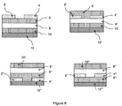
- the semiconductor materials of the present teachings can be used to fabricate various types of organic field effect transistors including top-gate top-contact capacitor structures, top-gate bottom-contact capacitor structures, bottom-gate top-contact capacitor structures, and bottom-gate bottom-contact capacitor structures.
- Figure 6 illustrates the four common types of OFET structures: top-contact bottom-gate structure (top left), bottom-contact bottom-gate structure (top right), bottom-contact top-gate structure (bottom left), and top-contact top-gate structure (bottom right).
- an OFET can include a dielectric layer (e.g., shown as 8, 8', 8", and 8"'), a semiconductor layer (e.g., shown as 6, 6', 6", and 6"'), a gate contact (e.g., shown as 10, 10', 10", and 10"'), a substrate (e.g., shown as 12, 12', 12", and 12'"), and source and drain contacts (e.g., shown as 2, 2', 2", 2'", 4, 4', 4", and 4'").
- a dielectric layer e.g., shown as 8, 8', 8", and 8"'
- a semiconductor layer e.g., shown as 6, 6', 6", and 6"'
- a gate contact e.g., shown as 10, 10', 10", and 10"'
- a substrate e.g., shown as 12, 12', 12", and 12'
- source and drain contacts e.g., shown as 2, 2', 2", 2'", 4, 4',
- OTFT devices can be fabricated with the present compounds on doped silicon substrates, using SiO 2 as the dielectric, in top-contact geometries.
- the active semiconducting layer which incorporates at least a compound of the present teachings can be deposited by vacuum vapor deposition at room temperature or at an elevated temperature.
- the active semiconducting layer which incorporates at least a compound of the present teachings can be applied by solution-based process, for example, spin-coating or jet printing.
- metallic contacts can be patterned on top of the films using shadow masks.
- OTFT devices can be fabricated with the present compounds on plastic foils, using polymers as the dielectric, in top-gate bottom-contact geometries.
- the active semiconducting layer which incorporates at least a compound of the present teachings can be deposited at room temperature or at an elevated temperature.
- the active semiconducting layer which incorporates at least a compound of the present teachings can be applied by spin-coating or printing as described herein.
- Gate and source/drain contacts can be made of Au, other metals, or conducting polymers and deposited by vapor-deposition and/or printing.
- compositions of the present teachings can exhibit broad optical absorption and/or a very positively shifted reduction potential making them desirable for such applications. Accordingly, the compounds described herein can be used as an n-type semiconductor in a photovoltaic design, which includes an adjacent p-type semiconducting material that forms a p-n junction.
- the compounds can be in the form of a thin film semiconductor, which can be a composite of the thin film semiconductor deposited on a substrate. Exploitation of compounds of the present teachings in such devices is within the knowledge of the skilled artisan.
- FIG. 7 illustrates a representative structure of a bulk-heterojunction organic photovoltaic device (also known as solar cell) which can incorporate one or more compounds of the present teachings as the donor and/or acceptor materials.
- a representative solar cell generally includes a substrate 20 (e.g., glass), an anode 22 (e.g., ITO), a cathode 26 (e.g., aluminium or calcium), and an active layer 24 between the anode and the cathode which can incorporate one or more compounds of the present teachings as the electron donor (p-channel) and/or electron acceptor (n-channel) materials.
- Figure 8 illustrates a representative structure of an OLED which can incorporate one or more compounds of the present teachings as electron-transporting and/or emissive and/or hole-transporting materials.
- an OLED generally includes a substrate 30 (not shown), a transparent anode 32 (e.g., ITO), a cathode 40 (e.g., metal), and one or more organic layers which can incorporate one or more compounds of the present teachings as hole-transporting (n-channel) (layer 34 as shown) and/or emissive (layer 36 as shown) and/or electron-transporting (p-channel) materials (layer 38 as shown).
- n-channel layer 34 as shown
- emissive layer 36 as shown
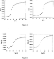
- p-channel electron-transporting
- Table 1 summarizes certain physical and electrical properties of some compounds of the present teachings, including E red values obtained from the cyclic voltammetry experiments.
- N,N'-Bis(4-n-octyl)-1,7-dicyanoperylene-3,4:9,10-bis(dicarboximide) (PDI8-CN 2 ), N,N'-bis[(3 S )-3,7-dimethyl-6-octenyl]-1,7-dicyanoperylene-3,4:9,10-bis(dicarboximide) (PDICitr-CN 2 ), N,N'-bis(2-ethylhexyl)-1,7-dicyanoperylene-3,4:9,10-bis(dicarboximide) (PDI2EH-CN 2 ), and N,N'-bis(2-methylhexyl)-1,7-dicyanoperylene-3,4:9,10-bis(dicarboximide) (PDI
- compounds of the present teachings can exhibit solubilities as high as 50 mg/mL, for example, in cold organic solvents such as chloroform and dichlorobenzene. Greater solubilities (2-10 times) can be achieved using warm solvents.
- perylene compounds having imide nitrogens functionalized with 1-alkyl substituted alkyl groups e.g., PDI1MH-CN 2 , PDI1MP-CN 2 , and PDI1M3MB-CN 2
- PDI1MH-CN 2 PDI1MH-CN 2
- PDI1MP-CN 2 PDI1MP-CN 2
- PDI1M3MB-CN 2 perylene compounds having imide nitrogens functionalized with 1-alkyl substituted alkyl groups
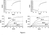
- Thin-film transistor (TFT) devices (25-200 ⁇ m channel lengths ( L ) and 1.0-4.0 mm channel widths ( W )) were fabricated with compounds of the present teachings using the top-contact configuration.
- Semiconductors films prepared with compounds of the present teachings were vacuum vapor-deposited (2 - 4 ⁇ s -1 , P ⁇ 10 -6 Torr) or spin coated on n-doped Si/SiO 2 (300 nm thick thermal oxide) substrates, which had been pretreated with hexamethyldisilazane. XRD plots of these semiconductor films show sharp reflections, suggesting high crystallinity.
- the gate region was accessed by an ohmic contact to the Si substrate, and Au source and drain contacts were evaporated through a shadow mask onto the semiconductor layer. All electrical measurements were performed in ambient atmosphere. Data reported below are average values measured from at least three devices tested at different locations on the semiconductor film.
- mobilities ( ⁇ ) were calculated by standard field effect transistor equations.
- MISFETs metal-insulator-semiconductor FETs
- I DS the source-drain saturation current
- V DS the potential between the source and drain
- V G the gate voltage
- I DS sat WC i / 2 L ⁇ V G ⁇ V t 2
- L and W are the device channel length and width, respectively
- C i is the capacitance of the oxide insulator ( ⁇ 1 ⁇ 10 -8 F/cm 2 for ⁇ 300 nm SiO 2 )
- V t is the threshold voltage.
- Table 2 summarizes electron mobilities and current on/off ratios of certain compounds of the present teachings and comparative representative compounds that were formed into thin layer semiconductors by vacuum-deposition, spin-coating, or drop-casting.
- perylene compounds having imide nitrogens functionalized with 1-alkyl substituted alkyl groups showed an unexpected increase in current I on :I off ratio compared to similar compounds substituted with slightly different alkyl or alkenyl groups (i.e., PDI8-CN 2 and PDICitr-CN 2 ).
- certain compounds of the present teachings demonstrated an unexpected higher electron mobility than similar known compounds such as PDI8-CN 2 and PDICitr-CN 2 .
Claims (12)
- Verbindung der Formel I:
 R1 und R2 bei jedem Auftreten unabhängig aus einer C1-12-Alkylgruppe, einer C1-12-Halogenalkylgruppe und einer Phenylgruppe, die gegebenenfalls durch 1-4 Gruppen, die unabhängig aus Halogen, einer C1-6-Alkylgruppe und einer C1-6-Halogenalkylgruppe ausgewählt sind, substituiert ist, ausgewählt sind;R3, R4, R5 und R6 unabhängig für H oder eine elektronenanziehende Gruppe, die aus Br und -CN ausgewählt ist, stehen, wobei entweder (i) jede der Variablen R3 und R4 für Br oder -CN steht, während jede der Variablen R5 und R6 für H steht oder (ii) jede der Variablen R3 und R6 für Br oder -CN steht, während jede der Variablen R4 und R5 für H steht.
 - Verbindung nach Anspruch 1, wobei R1 bei jedem Auftreten aus einer C1-12-Alkylgruppe und einer Phenylgruppe, die gegebenenfalls durch eine C1-6-Alkylgruppe substituiert ist, ausgewählt ist und R2 bei jedem Auftreten aus einer C1-6-Alkylgruppe und einer C1-6-Halogenalkylgruppe ausgewählt ist.
- Verbindung nach Anspruch 1 oder 2, wobei die Verbindung eine Formel aufweist, die aus der Gruppe bestehend aus:


- Verbindung nach Anspruch 1 oder 2, wobei die Verbindung eine Formel aufweist, die aus der Gruppe bestehend aus:


- Verfahren zur Herstellung der Verbindung nach einem der Ansprüche 1-3, wobei es sich bei der elektronenanziehenden Gruppe um -CN handelt, bei dem man eine Verbindung der Formel II:

wobei:R1 und R2 bei jedem Auftreten unabhängig aus einer C1-12-Alkylgruppe, einer C1-12-Halogenalkylgruppe und einer Phenylgruppe, die gegebenenfalls durch 1-4 Gruppen, die unabhängig aus Halogen, einer C1-6-Alkylgruppe und einer C1-6-Halogenalkylgruppe ausgewählt sind, substituiert ist, ausgewählt sind;X bei jedem Auftreten für H oder Br steht, wobei zwei X für Br stehen und zwei X für H stehen; n für 1, 2, 3 oder 4 steht. - Verfahren nach Anspruch 5, bei dem die Verbindung der Formel II durch Umsetzung einer Verbindung der Formel III:


- Verfahren nach Anspruch 5 oder 6, bei dem die Verbindung der Formel II aus:


- Erzeugnis, wobei es sich bei dem Erzeugnis um eine elektronische Vorrichtung, eine optische Vorrichtung oder eine optoelektronische Vorrichtung handelt, die eine oder mehrere Verbindungen nach einem der Ansprüche 1-4 umfasst.
- Erzeugnis nach Anspruch 8, wobei es sich bei dem Erzeugnis um eine Feldeffekttransistorvorrichtung handelt, die einen Dünnschichthalbleiter umfasst, der eine oder mehrere Verbindungen nach einem der Ansprüche 1 bis 4 umfasst.
- Erzeugnis nach Anspruch 8, wobei es sich bei dem Erzeugnis um eine Photovoltaikvorrichtung handelt, die einen Dünnschichthalbleiter umfasst, der eine oder mehrere Verbindungen nach einem der Ansprüche 1 bis 4 umfasst.
- Erzeugnis nach Anspruch 8, wobei es sich bei dem Erzeugnis um eine organische Leuchtdiodenvorrichtung handelt, die einen Dünnschichthalbleiter umfasst, der eine oder mehrere Verbindungen nach einem der Ansprüche 1 bis 4 umfasst.
- Erzeugnis nach Anspruch 8, wobei es sich bei dem Erzeugnis um eine unipolare oder komplementäre Schaltungsvorrichtung handelt, die einen Dünnschichthalbleiter umfasst, der eine oder mehrere Verbindungen nach einem der Ansprüche 1 bis 4 umfasst.
Applications Claiming Priority (2)
| Application Number | Priority Date | Filing Date | Title |
|---|---|---|---|
| US2631108P | 2008-02-05 | 2008-02-05 | |
| PCT/EP2009/051313 WO2009098252A1 (en) | 2008-02-05 | 2009-02-05 | Perylene semiconductors and methods of preparation and use thereof |
Publications (2)
| Publication Number | Publication Date |
|---|---|
| EP2240970A1 EP2240970A1 (de) | 2010-10-20 |
| EP2240970B1 true EP2240970B1 (de) | 2018-03-14 |
Family
ID=40580468
Family Applications (1)
| Application Number | Title | Priority Date | Filing Date |
|---|---|---|---|
| EP09709379.3A Active EP2240970B1 (de) | 2008-02-05 | 2009-02-05 | Perylen-halbleiter und methoden zu deren herstellung |
Country Status (8)
| Country | Link |
|---|---|
| US (1) | US8404844B2 (de) |
| EP (1) | EP2240970B1 (de) |
| JP (1) | JP5523351B2 (de) |
| KR (2) | KR101638199B1 (de) |
| CN (1) | CN101952988B (de) |
| CA (1) | CA2714423A1 (de) |
| TW (2) | TWI534146B (de) |
| WO (1) | WO2009098252A1 (de) |
Families Citing this family (61)
| Publication number | Priority date | Publication date | Assignee | Title |
|---|---|---|---|---|
| KR101717398B1 (ko) | 2008-11-24 | 2017-03-16 | 바스프 에스이 | 광경화성 중합체 유전체 및 이의 제조 및 이용 방법 |
| WO2010125011A2 (de) | 2009-04-28 | 2010-11-04 | Basf Se | Verfahren zur herstellung von halbleitenden schichten |
| EP2519523A1 (de) * | 2009-12-29 | 2012-11-07 | Polyera Corporation | Thionierte aromatische bisimide als organische halbleiter und vorrichtungen damit |
| US8580384B2 (en) | 2010-01-17 | 2013-11-12 | Polyera Corporation | Dielectric materials and methods of preparation and use thereof |
| WO2012090110A1 (en) * | 2010-12-30 | 2012-07-05 | Basf Se | Perylene-based semiconductors and methods of preparation and use thereof |
| WO2012095790A1 (en) * | 2011-01-10 | 2012-07-19 | Basf Se | Thiocyanato or isothiocyanato substituted naphthalene diimide and rylene diimide compounds and their use as n-type semiconductors |
| EP2681217A1 (de) * | 2011-03-03 | 2014-01-08 | Basf Se | Perylen-basierte halbleitermaterialien |
| US8471020B2 (en) | 2011-03-03 | 2013-06-25 | Basf Se | Perylene-based semiconducting materials |
| KR101805242B1 (ko) * | 2011-03-15 | 2017-12-06 | 바스프 에스이 | 테트라아자페로피렌 화합물 및 n-형 반도체로서의 그의 용도 |
| WO2012152598A1 (en) | 2011-05-11 | 2012-11-15 | Basf Se | Halogenated perylene-based semiconducting materials |
| JP6108329B2 (ja) * | 2011-08-15 | 2017-04-05 | 国立大学法人東京工業大学 | 有機半導体材料 |
| JP6161636B2 (ja) | 2012-02-07 | 2017-07-12 | フレックステラ, インコーポレイテッドFlexterra, Inc. | 光硬化性高分子材料および関連電子デバイス |
| US8901547B2 (en) | 2012-08-25 | 2014-12-02 | Polyera Corporation | Stacked structure organic light-emitting transistors |
| WO2014100961A1 (en) * | 2012-12-24 | 2014-07-03 | Rhodia Operations | Use of compounds of the perylene type as acceptors in photovoltaics |
| CN104045657B (zh) * | 2013-03-14 | 2017-07-21 | 中国科学院化学研究所 | 五元杂环衍生物桥联的苝二酰亚胺二聚体、其制备方法及其在有机光伏器件中的应用 |
| CN104177378A (zh) * | 2013-05-21 | 2014-12-03 | 中国科学院化学研究所 | 四取代的苝二酰亚胺二聚体、其制备方法及其在有机光伏器件中的应用 |
| US9541829B2 (en) | 2013-07-24 | 2017-01-10 | Orthogonal, Inc. | Cross-linkable fluorinated photopolymer |
| CN105659310B (zh) | 2013-08-13 | 2021-02-26 | 飞利斯有限公司 | 电子显示区域的优化 |
| WO2015031426A1 (en) | 2013-08-27 | 2015-03-05 | Polyera Corporation | Flexible display and detection of flex state |
| TWI655807B (zh) | 2013-08-27 | 2019-04-01 | 飛利斯有限公司 | 具有可撓曲電子構件之可附接裝置 |
| WO2015038684A1 (en) | 2013-09-10 | 2015-03-19 | Polyera Corporation | Attachable article with signaling, split display and messaging features |
| US9472771B2 (en) * | 2013-10-31 | 2016-10-18 | Sabic Global Technologies B.V. | Method of making axially fluorinated-phthalocyanines with an aprotic fluoride compound |
| CN103554106B (zh) * | 2013-11-14 | 2016-05-25 | 中国科学院化学研究所 | 胺基/氧化胺修饰的苝二酰亚胺衍生物,其制备方法及应用 |
| WO2015100224A1 (en) | 2013-12-24 | 2015-07-02 | Polyera Corporation | Flexible electronic display with user interface based on sensed movements |
| CN106031308B (zh) | 2013-12-24 | 2019-08-09 | 飞利斯有限公司 | 用于附接式二维挠性电子装置的支撑结构 |
| KR20160103072A (ko) | 2013-12-24 | 2016-08-31 | 폴리에라 코퍼레이션 | 가요성 전자 부품용 지지 구조체 |
| WO2015100396A1 (en) | 2013-12-24 | 2015-07-02 | Polyera Corporation | Support structures for a flexible electronic component |
| US9958778B2 (en) | 2014-02-07 | 2018-05-01 | Orthogonal, Inc. | Cross-linkable fluorinated photopolymer |
| US20150227245A1 (en) | 2014-02-10 | 2015-08-13 | Polyera Corporation | Attachable Device with Flexible Electronic Display Orientation Detection |
| US10261634B2 (en) | 2014-03-27 | 2019-04-16 | Flexterra, Inc. | Infrared touch system for flexible displays |
| KR102470798B1 (ko) * | 2014-05-09 | 2022-11-28 | 바스프 에스이 | 시안화 페릴렌 화합물 |
| US20170301477A1 (en) | 2016-04-04 | 2017-10-19 | Capacitor Sciences Incorporated | Electro-polarizable compound and capacitor |
| US10340082B2 (en) | 2015-05-12 | 2019-07-02 | Capacitor Sciences Incorporated | Capacitor and method of production thereof |
| US10347423B2 (en) | 2014-05-12 | 2019-07-09 | Capacitor Sciences Incorporated | Solid multilayer structure as semiproduct for meta-capacitor |
| WO2015175558A2 (en) | 2014-05-12 | 2015-11-19 | Capacitor Sciences Incorporated | Energy storage device and method of production thereof |
| TWI692272B (zh) | 2014-05-28 | 2020-04-21 | 美商飛利斯有限公司 | 在多數表面上具有可撓性電子組件之裝置 |
| WO2015183567A1 (en) | 2014-05-28 | 2015-12-03 | Polyera Corporation | Low power display updates |
| EP3183250B1 (de) | 2014-08-18 | 2023-10-04 | CLAP Co., Ltd. | Verfahren zur herstellung von kristallinem organischem halbleitermaterial |
| CN107207492A (zh) * | 2014-08-28 | 2017-09-26 | 巴斯夫欧洲公司 | 含有小分子半导体化合物和非导电聚合物的薄膜半导体 |
| RU2017112074A (ru) | 2014-11-04 | 2018-12-05 | Кэпэситор Сайенсиз Инкорпорейтед | Устройства для хранения энергии и способы их получения |
| US9812645B2 (en) | 2015-02-13 | 2017-11-07 | Flexterra, Inc. | Perylene-based semiconductors |
| WO2016138310A1 (en) | 2015-02-26 | 2016-09-01 | Capacitor Sciences Incorporated | Self-healing capacitor and methods of production thereof |
| WO2016138356A1 (en) | 2015-02-26 | 2016-09-01 | Polyera Corporation | Attachable device having a flexible electronic component |
| US9932358B2 (en) | 2015-05-21 | 2018-04-03 | Capacitor Science Incorporated | Energy storage molecular material, crystal dielectric layer and capacitor |
| US9941051B2 (en) | 2015-06-26 | 2018-04-10 | Capactor Sciences Incorporated | Coiled capacitor |
| KR101798976B1 (ko) * | 2015-09-21 | 2017-11-17 | 경희대학교 산학협력단 | 이산화탄소 흡수제 |
| US10026553B2 (en) | 2015-10-21 | 2018-07-17 | Capacitor Sciences Incorporated | Organic compound, crystal dielectric layer and capacitor |
| CN105732623B (zh) * | 2016-01-28 | 2019-05-28 | 燕山大学 | 苝酰亚胺及其衍生物的还原态离子盐的制备方法 |
| US20170233528A1 (en) * | 2016-02-12 | 2017-08-17 | Capacitor Sciences Incorporated | Sharp polymer and capacitor |
| US10305295B2 (en) | 2016-02-12 | 2019-05-28 | Capacitor Sciences Incorporated | Energy storage cell, capacitive energy storage module, and capacitive energy storage system |
| US10153087B2 (en) | 2016-04-04 | 2018-12-11 | Capacitor Sciences Incorporated | Electro-polarizable compound and capacitor |
| US9978517B2 (en) | 2016-04-04 | 2018-05-22 | Capacitor Sciences Incorporated | Electro-polarizable compound and capacitor |
| KR102303315B1 (ko) | 2016-05-25 | 2021-09-23 | 주식회사 클랩 | 반도체 |
| CN107523290B (zh) * | 2016-06-20 | 2019-10-18 | 国家纳米科学中心 | 一种有机分子二维有序结构及其制备方法 |
| CN109478595B (zh) * | 2016-06-27 | 2023-02-07 | 富士胶片株式会社 | 有机薄膜晶体管、有机半导体膜、化合物、有机薄膜晶体管用组合物及有机薄膜晶体管的制造方法 |
| US10395841B2 (en) | 2016-12-02 | 2019-08-27 | Capacitor Sciences Incorporated | Multilayered electrode and film energy storage device |
| TW201835300A (zh) * | 2016-12-22 | 2018-10-01 | 德商麥克專利有限公司 | 包含至少二種有機官能性化合物之混合物 |
| WO2019144082A1 (en) | 2018-01-19 | 2019-07-25 | Flexterra, Inc. | Organic dielectric materials and devices including them |
| EP3664171B1 (de) | 2018-12-06 | 2021-05-12 | Flexterra, Inc. | Dünnschichttransistor mit organischen halbleitermaterialien |
| CN110845505B (zh) * | 2019-11-18 | 2022-03-29 | 陕西理工大学 | 苝二酰亚胺衍生物及基于其的电学阻抗型区分检测吡啶衍生物传感器及其制备方法和应用 |
| CN113603688B (zh) * | 2021-06-23 | 2022-11-18 | 南京邮电大学 | 一种n型有机界面材料及其制备方法与应用 |
Family Cites Families (14)
| Publication number | Priority date | Publication date | Assignee | Title |
|---|---|---|---|---|
| DE19848555A1 (de) * | 1998-10-21 | 2000-04-27 | Heinz Langhals | Neue Fluoreszenzfarbstoffe durch Kern-Erweiterung von Perylen-3,4:9,10-tetracarbonsäurebisimiden |
| JP4053289B2 (ja) * | 2001-12-12 | 2008-02-27 | 本田技研工業株式会社 | 蓄電池の温度制御装置、及びそれを用いた車両装置 |
| DE10225595A1 (de) * | 2002-06-07 | 2003-12-18 | Basf Ag | 1,6,9,14-Tetrasubstituierte Terrylentetracarbonsäurediimide |
| JP4921982B2 (ja) | 2004-01-26 | 2012-04-25 | ノースウエスタン ユニバーシティ | ペリレンn型半導体及び関連装置 |
| US7422777B2 (en) * | 2005-11-22 | 2008-09-09 | Eastman Kodak Company | N,N′-dicycloalkyl-substituted naphthalene-based tetracarboxylic diimide compounds as n-type semiconductor materials for thin film transistors |
| EP1843407A1 (de) * | 2006-04-07 | 2007-10-10 | Basf Aktiengesellschaft | Flüssig-kristalline Rylentetracarbonsäurederivate und deren Verwendung |
| WO2007128774A1 (en) * | 2006-05-04 | 2007-11-15 | Basf Se | Method for producing organic field-effect transistors |
| US7569693B2 (en) | 2006-06-12 | 2009-08-04 | Northwestern University | Naphthalene-based semiconductor materials and methods of preparing and use thereof |
| WO2008051552A2 (en) | 2006-10-25 | 2008-05-02 | Northwestern University | Organic semiconductor materials and methods of preparing and use thereof |
| EP2086974B1 (de) | 2006-11-17 | 2013-07-24 | Polyera Corporation | Halbleitermaterialien auf diimidbasis und verfahren zu deren herstellung und anwendung |
| US7892454B2 (en) | 2006-11-17 | 2011-02-22 | Polyera Corporation | Acene-based organic semiconductor materials and methods of preparing and using the same |
| WO2008085942A2 (en) | 2007-01-08 | 2008-07-17 | Polyera Corporation | Methods for preparing arene-bis(dicarboximide)-based semiconducting materials and related intermediates for preparing same |
| WO2008091670A2 (en) | 2007-01-24 | 2008-07-31 | Polyera Corporation | Organic semiconductor materials and precursors thereof |
| EP2626359B1 (de) * | 2007-05-09 | 2014-08-06 | Yeda Research and Development Co. Ltd. | Perylendiimide |
-
2009
- 2009-02-05 CN CN200980104236.7A patent/CN101952988B/zh active Active
- 2009-02-05 EP EP09709379.3A patent/EP2240970B1/de active Active
- 2009-02-05 TW TW103111814A patent/TWI534146B/zh active
- 2009-02-05 TW TW098103786A patent/TWI439461B/zh active
- 2009-02-05 KR KR1020107018813A patent/KR101638199B1/ko active IP Right Grant
- 2009-02-05 JP JP2010545463A patent/JP5523351B2/ja active Active
- 2009-02-05 CA CA2714423A patent/CA2714423A1/en not_active Abandoned
- 2009-02-05 KR KR1020167005082A patent/KR20160029863A/ko not_active Application Discontinuation
- 2009-02-05 WO PCT/EP2009/051313 patent/WO2009098252A1/en active Application Filing
- 2009-02-05 US US12/866,331 patent/US8404844B2/en active Active
Also Published As
| Publication number | Publication date |
|---|---|
| WO2009098252A1 (en) | 2009-08-13 |
| TW201006840A (en) | 2010-02-16 |
| KR20100108605A (ko) | 2010-10-07 |
| JP2011514884A (ja) | 2011-05-12 |
| CN101952988A (zh) | 2011-01-19 |
| US20100319778A1 (en) | 2010-12-23 |
| CN101952988B (zh) | 2015-12-16 |
| KR20160029863A (ko) | 2016-03-15 |
| TWI534146B (zh) | 2016-05-21 |
| JP5523351B2 (ja) | 2014-06-18 |
| CA2714423A1 (en) | 2009-08-13 |
| TWI439461B (zh) | 2014-06-01 |
| EP2240970A1 (de) | 2010-10-20 |
| KR101638199B1 (ko) | 2016-07-08 |
| US8404844B2 (en) | 2013-03-26 |
| TW201446764A (zh) | 2014-12-16 |
Similar Documents
| Publication | Publication Date | Title |
|---|---|---|
| EP2240970B1 (de) | Perylen-halbleiter und methoden zu deren herstellung | |
| EP2086974B1 (de) | Halbleitermaterialien auf diimidbasis und verfahren zu deren herstellung und anwendung | |
| US7892454B2 (en) | Acene-based organic semiconductor materials and methods of preparing and using the same | |
| US8569501B2 (en) | Semiconductor materials and methods of preparation and use thereof | |
| US8440828B2 (en) | Organic semiconductors and devices incorporating same | |
| EP2683718B1 (de) | Thiocyanat substituierte naphthalen-diimid-verbindungen sowie verwendung davon als n-halbleiter | |
| US8022214B2 (en) | Organic semiconductor materials and precursors thereof | |
| JP2010510228A5 (de) | ||
| US9147850B2 (en) | Perylene-based semiconductors and methods of preparation and use thereof | |
| EP2686322B1 (de) | Tetraazaperopyrenverbindungen und ihre verwendung als n-halbleiter | |
| US8513445B2 (en) | Polycyclic aromatic molecular semiconductors and related compositions and devices | |
| US9812645B2 (en) | Perylene-based semiconductors |
Legal Events
| Date | Code | Title | Description |
|---|---|---|---|
| PUAI | Public reference made under article 153(3) epc to a published international application that has entered the european phase |
Free format text: ORIGINAL CODE: 0009012 |
|
| 17P | Request for examination filed |
Effective date: 20100906 |
|
| AK | Designated contracting states |
Kind code of ref document: A1 Designated state(s): AT BE BG CH CY CZ DE DK EE ES FI FR GB GR HR HU IE IS IT LI LT LU LV MC MK MT NL NO PL PT RO SE SI SK TR |
|
| AX | Request for extension of the european patent |
Extension state: AL BA RS |
|
| DAX | Request for extension of the european patent (deleted) | ||
| 17Q | First examination report despatched |
Effective date: 20160719 |
|
| STAA | Information on the status of an ep patent application or granted ep patent |
Free format text: STATUS: EXAMINATION IS IN PROGRESS |
|
| RAP1 | Party data changed (applicant data changed or rights of an application transferred) |
Owner name: FLEXTERRA, INC. Owner name: BASF SE |
|
| GRAP | Despatch of communication of intention to grant a patent |
Free format text: ORIGINAL CODE: EPIDOSNIGR1 |
|
| STAA | Information on the status of an ep patent application or granted ep patent |
Free format text: STATUS: GRANT OF PATENT IS INTENDED |
|
| INTG | Intention to grant announced |
Effective date: 20170904 |
|
| GRAS | Grant fee paid |
Free format text: ORIGINAL CODE: EPIDOSNIGR3 |
|
| GRAA | (expected) grant |
Free format text: ORIGINAL CODE: 0009210 |
|
| STAA | Information on the status of an ep patent application or granted ep patent |
Free format text: STATUS: THE PATENT HAS BEEN GRANTED |
|
| AK | Designated contracting states |
Kind code of ref document: B1 Designated state(s): AT BE BG CH CY CZ DE DK EE ES FI FR GB GR HR HU IE IS IT LI LT LU LV MC MK MT NL NO PL PT RO SE SI SK TR |
|
| REG | Reference to a national code |
Ref country code: GB Ref legal event code: FG4D |
|
| REG | Reference to a national code |
Ref country code: CH Ref legal event code: EP Ref country code: AT Ref legal event code: REF Ref document number: 979658 Country of ref document: AT Kind code of ref document: T Effective date: 20180315 |
|
| REG | Reference to a national code |
Ref country code: IE Ref legal event code: FG4D |
|
| REG | Reference to a national code |
Ref country code: DE Ref legal event code: R096 Ref document number: 602009051222 Country of ref document: DE |
|
| REG | Reference to a national code |
Ref country code: NL Ref legal event code: MP Effective date: 20180314 |
|
| REG | Reference to a national code |
Ref country code: LT Ref legal event code: MG4D |
|
| PG25 | Lapsed in a contracting state [announced via postgrant information from national office to epo] |
Ref country code: ES Free format text: LAPSE BECAUSE OF FAILURE TO SUBMIT A TRANSLATION OF THE DESCRIPTION OR TO PAY THE FEE WITHIN THE PRESCRIBED TIME-LIMIT Effective date: 20180314 Ref country code: FI Free format text: LAPSE BECAUSE OF FAILURE TO SUBMIT A TRANSLATION OF THE DESCRIPTION OR TO PAY THE FEE WITHIN THE PRESCRIBED TIME-LIMIT Effective date: 20180314 Ref country code: NO Free format text: LAPSE BECAUSE OF FAILURE TO SUBMIT A TRANSLATION OF THE DESCRIPTION OR TO PAY THE FEE WITHIN THE PRESCRIBED TIME-LIMIT Effective date: 20180614 Ref country code: CY Free format text: LAPSE BECAUSE OF FAILURE TO SUBMIT A TRANSLATION OF THE DESCRIPTION OR TO PAY THE FEE WITHIN THE PRESCRIBED TIME-LIMIT Effective date: 20180314 Ref country code: LT Free format text: LAPSE BECAUSE OF FAILURE TO SUBMIT A TRANSLATION OF THE DESCRIPTION OR TO PAY THE FEE WITHIN THE PRESCRIBED TIME-LIMIT Effective date: 20180314 Ref country code: HR Free format text: LAPSE BECAUSE OF FAILURE TO SUBMIT A TRANSLATION OF THE DESCRIPTION OR TO PAY THE FEE WITHIN THE PRESCRIBED TIME-LIMIT Effective date: 20180314 |
|
| REG | Reference to a national code |
Ref country code: AT Ref legal event code: MK05 Ref document number: 979658 Country of ref document: AT Kind code of ref document: T Effective date: 20180314 |
|
| PG25 | Lapsed in a contracting state [announced via postgrant information from national office to epo] |
Ref country code: BG Free format text: LAPSE BECAUSE OF FAILURE TO SUBMIT A TRANSLATION OF THE DESCRIPTION OR TO PAY THE FEE WITHIN THE PRESCRIBED TIME-LIMIT Effective date: 20180614 Ref country code: GR Free format text: LAPSE BECAUSE OF FAILURE TO SUBMIT A TRANSLATION OF THE DESCRIPTION OR TO PAY THE FEE WITHIN THE PRESCRIBED TIME-LIMIT Effective date: 20180615 Ref country code: SE Free format text: LAPSE BECAUSE OF FAILURE TO SUBMIT A TRANSLATION OF THE DESCRIPTION OR TO PAY THE FEE WITHIN THE PRESCRIBED TIME-LIMIT Effective date: 20180314 Ref country code: LV Free format text: LAPSE BECAUSE OF FAILURE TO SUBMIT A TRANSLATION OF THE DESCRIPTION OR TO PAY THE FEE WITHIN THE PRESCRIBED TIME-LIMIT Effective date: 20180314 |
|
| PG25 | Lapsed in a contracting state [announced via postgrant information from national office to epo] |
Ref country code: RO Free format text: LAPSE BECAUSE OF FAILURE TO SUBMIT A TRANSLATION OF THE DESCRIPTION OR TO PAY THE FEE WITHIN THE PRESCRIBED TIME-LIMIT Effective date: 20180314 Ref country code: EE Free format text: LAPSE BECAUSE OF FAILURE TO SUBMIT A TRANSLATION OF THE DESCRIPTION OR TO PAY THE FEE WITHIN THE PRESCRIBED TIME-LIMIT Effective date: 20180314 Ref country code: PL Free format text: LAPSE BECAUSE OF FAILURE TO SUBMIT A TRANSLATION OF THE DESCRIPTION OR TO PAY THE FEE WITHIN THE PRESCRIBED TIME-LIMIT Effective date: 20180314 Ref country code: NL Free format text: LAPSE BECAUSE OF FAILURE TO SUBMIT A TRANSLATION OF THE DESCRIPTION OR TO PAY THE FEE WITHIN THE PRESCRIBED TIME-LIMIT Effective date: 20180314 |
|
| PG25 | Lapsed in a contracting state [announced via postgrant information from national office to epo] |
Ref country code: SK Free format text: LAPSE BECAUSE OF FAILURE TO SUBMIT A TRANSLATION OF THE DESCRIPTION OR TO PAY THE FEE WITHIN THE PRESCRIBED TIME-LIMIT Effective date: 20180314 Ref country code: CZ Free format text: LAPSE BECAUSE OF FAILURE TO SUBMIT A TRANSLATION OF THE DESCRIPTION OR TO PAY THE FEE WITHIN THE PRESCRIBED TIME-LIMIT Effective date: 20180314 Ref country code: AT Free format text: LAPSE BECAUSE OF FAILURE TO SUBMIT A TRANSLATION OF THE DESCRIPTION OR TO PAY THE FEE WITHIN THE PRESCRIBED TIME-LIMIT Effective date: 20180314 |
|
| REG | Reference to a national code |
Ref country code: DE Ref legal event code: R097 Ref document number: 602009051222 Country of ref document: DE |
|
| PG25 | Lapsed in a contracting state [announced via postgrant information from national office to epo] |
Ref country code: PT Free format text: LAPSE BECAUSE OF FAILURE TO SUBMIT A TRANSLATION OF THE DESCRIPTION OR TO PAY THE FEE WITHIN THE PRESCRIBED TIME-LIMIT Effective date: 20180716 |
|
| PLBE | No opposition filed within time limit |
Free format text: ORIGINAL CODE: 0009261 |
|
| STAA | Information on the status of an ep patent application or granted ep patent |
Free format text: STATUS: NO OPPOSITION FILED WITHIN TIME LIMIT |
|
| PG25 | Lapsed in a contracting state [announced via postgrant information from national office to epo] |
Ref country code: DK Free format text: LAPSE BECAUSE OF FAILURE TO SUBMIT A TRANSLATION OF THE DESCRIPTION OR TO PAY THE FEE WITHIN THE PRESCRIBED TIME-LIMIT Effective date: 20180314 |
|
| 26N | No opposition filed |
Effective date: 20181217 |
|
| PG25 | Lapsed in a contracting state [announced via postgrant information from national office to epo] |
Ref country code: SI Free format text: LAPSE BECAUSE OF FAILURE TO SUBMIT A TRANSLATION OF THE DESCRIPTION OR TO PAY THE FEE WITHIN THE PRESCRIBED TIME-LIMIT Effective date: 20180314 |
|
| REG | Reference to a national code |
Ref country code: DE Ref legal event code: R081 Ref document number: 602009051222 Country of ref document: DE Owner name: FLEXTERRA, INC., SKOKIE, US Free format text: FORMER OWNERS: BASF SE, 67063 LUDWIGSHAFEN, DE; FLEXTERRA, INC., SKOKIE, ILL., US |
|
| REG | Reference to a national code |
Ref country code: GB Ref legal event code: 732E Free format text: REGISTERED BETWEEN 20190516 AND 20190522 |
|
| REG | Reference to a national code |
Ref country code: CH Ref legal event code: PL |
|
| PG25 | Lapsed in a contracting state [announced via postgrant information from national office to epo] |
Ref country code: LU Free format text: LAPSE BECAUSE OF NON-PAYMENT OF DUE FEES Effective date: 20190205 Ref country code: MC Free format text: LAPSE BECAUSE OF FAILURE TO SUBMIT A TRANSLATION OF THE DESCRIPTION OR TO PAY THE FEE WITHIN THE PRESCRIBED TIME-LIMIT Effective date: 20180314 |
|
| REG | Reference to a national code |
Ref country code: BE Ref legal event code: MM Effective date: 20190228 |
|
| REG | Reference to a national code |
Ref country code: IE Ref legal event code: MM4A |
|
| PG25 | Lapsed in a contracting state [announced via postgrant information from national office to epo] |
Ref country code: LI Free format text: LAPSE BECAUSE OF NON-PAYMENT OF DUE FEES Effective date: 20190228 Ref country code: CH Free format text: LAPSE BECAUSE OF NON-PAYMENT OF DUE FEES Effective date: 20190228 |
|
| PG25 | Lapsed in a contracting state [announced via postgrant information from national office to epo] |
Ref country code: IE Free format text: LAPSE BECAUSE OF NON-PAYMENT OF DUE FEES Effective date: 20190205 |
|
| PG25 | Lapsed in a contracting state [announced via postgrant information from national office to epo] |
Ref country code: BE Free format text: LAPSE BECAUSE OF NON-PAYMENT OF DUE FEES Effective date: 20190228 |
|
| PG25 | Lapsed in a contracting state [announced via postgrant information from national office to epo] |
Ref country code: TR Free format text: LAPSE BECAUSE OF FAILURE TO SUBMIT A TRANSLATION OF THE DESCRIPTION OR TO PAY THE FEE WITHIN THE PRESCRIBED TIME-LIMIT Effective date: 20180314 |
|
| PG25 | Lapsed in a contracting state [announced via postgrant information from national office to epo] |
Ref country code: MT Free format text: LAPSE BECAUSE OF NON-PAYMENT OF DUE FEES Effective date: 20190205 |
|
| PG25 | Lapsed in a contracting state [announced via postgrant information from national office to epo] |
Ref country code: IS Free format text: LAPSE BECAUSE OF FAILURE TO SUBMIT A TRANSLATION OF THE DESCRIPTION OR TO PAY THE FEE WITHIN THE PRESCRIBED TIME-LIMIT Effective date: 20180714 |
|
| PG25 | Lapsed in a contracting state [announced via postgrant information from national office to epo] |
Ref country code: HU Free format text: LAPSE BECAUSE OF FAILURE TO SUBMIT A TRANSLATION OF THE DESCRIPTION OR TO PAY THE FEE WITHIN THE PRESCRIBED TIME-LIMIT; INVALID AB INITIO Effective date: 20090205 |
|
| PG25 | Lapsed in a contracting state [announced via postgrant information from national office to epo] |
Ref country code: MK Free format text: LAPSE BECAUSE OF FAILURE TO SUBMIT A TRANSLATION OF THE DESCRIPTION OR TO PAY THE FEE WITHIN THE PRESCRIBED TIME-LIMIT Effective date: 20180314 |
|
| REG | Reference to a national code |
Ref country code: DE Ref legal event code: R079 Ref document number: 602009051222 Country of ref document: DE Free format text: PREVIOUS MAIN CLASS: H01L0051300000 Ipc: H10K0085000000 |
|
| PGFP | Annual fee paid to national office [announced via postgrant information from national office to epo] |
Ref country code: FR Payment date: 20230223 Year of fee payment: 15 |
|
| PGFP | Annual fee paid to national office [announced via postgrant information from national office to epo] |
Ref country code: IT Payment date: 20230221 Year of fee payment: 15 |
|
| P01 | Opt-out of the competence of the unified patent court (upc) registered |
Effective date: 20230521 |
|
| PGFP | Annual fee paid to national office [announced via postgrant information from national office to epo] |
Ref country code: DE Payment date: 20240228 Year of fee payment: 16 Ref country code: GB Payment date: 20240227 Year of fee payment: 16 |