EP2237332B1 - Light emitting device - Google Patents
Light emitting device Download PDFInfo
- Publication number
- EP2237332B1 EP2237332B1 EP09704913.4A EP09704913A EP2237332B1 EP 2237332 B1 EP2237332 B1 EP 2237332B1 EP 09704913 A EP09704913 A EP 09704913A EP 2237332 B1 EP2237332 B1 EP 2237332B1
- Authority
- EP
- European Patent Office
- Prior art keywords
- layer
- light emitting
- emitting device
- photonic crystal
- semiconductor layer
- Prior art date
- Legal status (The legal status is an assumption and is not a legal conclusion. Google has not performed a legal analysis and makes no representation as to the accuracy of the status listed.)
- Active
Links
Images


Classifications
-
- H—ELECTRICITY
- H10—SEMICONDUCTOR DEVICES; ELECTRIC SOLID-STATE DEVICES NOT OTHERWISE PROVIDED FOR
- H10H—INORGANIC LIGHT-EMITTING SEMICONDUCTOR DEVICES HAVING POTENTIAL BARRIERS
- H10H20/00—Individual inorganic light-emitting semiconductor devices having potential barriers, e.g. light-emitting diodes [LED]
- H10H20/80—Constructional details
- H10H20/83—Electrodes
- H10H20/832—Electrodes characterised by their material
- H10H20/835—Reflective materials
-
- H—ELECTRICITY
- H10—SEMICONDUCTOR DEVICES; ELECTRIC SOLID-STATE DEVICES NOT OTHERWISE PROVIDED FOR
- H10H—INORGANIC LIGHT-EMITTING SEMICONDUCTOR DEVICES HAVING POTENTIAL BARRIERS
- H10H20/00—Individual inorganic light-emitting semiconductor devices having potential barriers, e.g. light-emitting diodes [LED]
- H10H20/80—Constructional details
- H10H20/83—Electrodes
- H10H20/832—Electrodes characterised by their material
- H10H20/833—Transparent materials
-
- H—ELECTRICITY
- H10—SEMICONDUCTOR DEVICES; ELECTRIC SOLID-STATE DEVICES NOT OTHERWISE PROVIDED FOR
- H10H—INORGANIC LIGHT-EMITTING SEMICONDUCTOR DEVICES HAVING POTENTIAL BARRIERS
- H10H20/00—Individual inorganic light-emitting semiconductor devices having potential barriers, e.g. light-emitting diodes [LED]
- H10H20/80—Constructional details
- H10H20/84—Coatings, e.g. passivation layers or antireflective coatings
-
- H—ELECTRICITY
- H10—SEMICONDUCTOR DEVICES; ELECTRIC SOLID-STATE DEVICES NOT OTHERWISE PROVIDED FOR
- H10H—INORGANIC LIGHT-EMITTING SEMICONDUCTOR DEVICES HAVING POTENTIAL BARRIERS
- H10H20/00—Individual inorganic light-emitting semiconductor devices having potential barriers, e.g. light-emitting diodes [LED]
- H10H20/01—Manufacture or treatment
- H10H20/011—Manufacture or treatment of bodies, e.g. forming semiconductor layers
- H10H20/018—Bonding of wafers
-
- H—ELECTRICITY
- H10—SEMICONDUCTOR DEVICES; ELECTRIC SOLID-STATE DEVICES NOT OTHERWISE PROVIDED FOR
- H10H—INORGANIC LIGHT-EMITTING SEMICONDUCTOR DEVICES HAVING POTENTIAL BARRIERS
- H10H20/00—Individual inorganic light-emitting semiconductor devices having potential barriers, e.g. light-emitting diodes [LED]
- H10H20/80—Constructional details
- H10H20/81—Bodies
- H10H20/819—Bodies characterised by their shape, e.g. curved or truncated substrates
-
- H—ELECTRICITY
- H10—SEMICONDUCTOR DEVICES; ELECTRIC SOLID-STATE DEVICES NOT OTHERWISE PROVIDED FOR
- H10H—INORGANIC LIGHT-EMITTING SEMICONDUCTOR DEVICES HAVING POTENTIAL BARRIERS
- H10H20/00—Individual inorganic light-emitting semiconductor devices having potential barriers, e.g. light-emitting diodes [LED]
- H10H20/80—Constructional details
- H10H20/81—Bodies
- H10H20/822—Materials of the light-emitting regions
- H10H20/824—Materials of the light-emitting regions comprising only Group III-V materials, e.g. GaP
- H10H20/825—Materials of the light-emitting regions comprising only Group III-V materials, e.g. GaP containing nitrogen, e.g. GaN
-
- H—ELECTRICITY
- H10—SEMICONDUCTOR DEVICES; ELECTRIC SOLID-STATE DEVICES NOT OTHERWISE PROVIDED FOR
- H10H—INORGANIC LIGHT-EMITTING SEMICONDUCTOR DEVICES HAVING POTENTIAL BARRIERS
- H10H20/00—Individual inorganic light-emitting semiconductor devices having potential barriers, e.g. light-emitting diodes [LED]
- H10H20/80—Constructional details
- H10H20/84—Coatings, e.g. passivation layers or antireflective coatings
- H10H20/841—Reflective coatings, e.g. dielectric Bragg reflectors
-
- H—ELECTRICITY
- H10—SEMICONDUCTOR DEVICES; ELECTRIC SOLID-STATE DEVICES NOT OTHERWISE PROVIDED FOR
- H10H—INORGANIC LIGHT-EMITTING SEMICONDUCTOR DEVICES HAVING POTENTIAL BARRIERS
- H10H20/00—Individual inorganic light-emitting semiconductor devices having potential barriers, e.g. light-emitting diodes [LED]
- H10H20/80—Constructional details
- H10H20/872—Periodic patterns for optical field-shaping, e.g. photonic bandgap structures
Definitions
- the present disclosure relates to a light emitting device.
- Nitride semiconductors have been studied in the fields of optical and high-output electron device development because of their high thermal stability and wide bandgap.
- researches for a nitride semiconductor light emitting device are focused on light emitting efficiency improvement.
- One method is to increase light coupling probability of electrons and holes injected in a light emitting layer in order to improve internal quantum efficiency.
- the other method is to increase light extraction efficiency in order to allow light formed in a light emitting layer to escape from a thin layer effectively.
- EP 1 855 327 A2 discloses a nitride-based light emitting device capable of achieving an enhancement in emission efficiency and an enhancement in reliability.
- This light emitting device includes a semiconductor layer and a light extracting layer arranged on the semiconductor layer and made of a material having a refractive index equal to or higher than a refractive index of the semiconductor layer.
- Other structures for light emitting diodes are disclosed in US 2003/0111667 A1 and US 2006/0186417 A1 .
- Embodiments provide a light emitting device having an optimized light extraction efficiency.
- the present invention is directed to a light emitting device as defined in the appended claim 1. Further advantageous embodiments of the present invention are as defined in the appended claims 2-15.
- the light emitting device in accordance with the present invention comprises: a reflective layer; a transparent oxide layer on the reflective layer; a semiconductor layer on the transparent oxide layer, the semiconductor layer comprising a first semiconductor layer, a light emitting layer, and a second semiconductor layer, wherein a distance "d" between the reflective layer and a center of the light emitting layer corresponds to a constructive interference condition, and wherein the transparent oxide layer comprises: a first transparent conductive oxide layer on the reflective layer, an intermediate dielectric layer on the first conductive oxide layer, and a second transparent conductive oxide layer on the intermediate dielectric layer.
- a light emitting device obtains extraction efficiency improvement and output orientation by adjusting the distance "d" between the reflective layer and the light emitting layer.
- the adjusting of the distance "d” can be effectively accomplished through deposition of a semiconductor layer and a transparent oxide layer in accordance with the present invention.
- a distance "d" between the reflective layer and the light emitting layer can be adjusted by controlling a thickness of the transparent oxide layer during a deposition process, it is convenient to set the distance corresponding to the optimized light extraction efficiency.
- a light emitting device improves light extraction efficiency by forming a Photonic Crystal (PhC) structure as a light extraction structure, and also moves the optimum period at which light extraction efficiency is maximized, into a long period region, by adjusting an etching depth of the photonic crystal structure.
- PhC Photonic Crystal
- each layer is exaggerated, omitted, or schematically illustrated for convenience in description and clarity. Also, the size of each element does not entirely reflect an actual size.
- Fig. 1 is a cross-sectional view of a light emitting device according to an embodiment illustrative of the context of the present invention.
- the light emitting device can include a reflective layer 300 and a semiconductor layer 100.
- the semiconductor layer 100 includes a light emitting layer 120 above the reflective layer 300.
- a distance d between the reflective layer 300 and the center of the light emitting layer 120 can correspond to a constructive interference condition.
- Fig. 1 illustrates one example of a vertical light emitting device capable of maximizing light extraction efficiency.
- the reflective layer 300 can be disposed on a supporting layer 500
- a transparent oxide layer 400 such as a transparent conductive oxide can be disposed on the reflective layer 300
- the semiconductor layer 100 can be disposed on the layer 400.
- the semiconductor layer 100 can include a p-type semiconductor layer 130, the light emitting layer 120, and an n-type semiconductor layer 110.
- a photonic crystal (PhC) structure including hole 210 can be formed in the surface of the semiconductor layer 100, and an n-type electrode 600 can be formed on a region excluding the photonic crystal structure.
- a mask pattern (not shown) can be formed on the surface of the semiconductor layer 100, for example, the surface of the n-type semiconductor layer 110, and the hole 210 can be formed through a dry or wet etching process. As a result, the photonic crystal structure 200 can be formed.
- the distance d between the center of the light emitting layer 120 and the reflective layer 300 can correspond to the total thickness of the p-type GaN semiconductor layer 130 and the layer 400. Accordingly, within a range where electrical characteristics do not deteriorate, the thickness of the p-type GaN semiconductor layer 130 and the layer 400 having a radiation pattern in a vertical direction needs to be selected.
- the light emitting device can include an AlGaInP diode on a GaP substrate, a GaN diode on a SiC substrate, a SiC diode on a SiC substrate, a SiC diode on a sapphire substrate, etc.
- the layer 400 can be a transparent conductive oxide.
- Other materials such as an Indium-Zinc-Oxide (IZO), an Aluminum-Zinc-Oxide (AZO), a Magnesium-Zinc-Oxide (MZO), or a Gallium-Zinc-Oxide (GZO) can be used as the dielectric layer 400.
- the first embodiment can increase light extraction efficiency by adjusting a light emitting characteristic of the light emitting layer 120. For example, because of an interference effect between light generated in the light emitting layer 120 and light reflected from the reflective layer 300, an output radiation pattern can be adjusted.
- the reflective layer 300 is close to the light emitting layer 120 within a range where a radiation pattern can be adjusted, constructive interference occurrence in a vertical direction can be advantageous in terms of light extraction efficiency.
- Fig. 2 is a view illustrating an increase rate of light extraction efficiency according to an interval between a reflective layer (e.g., a mirror) and a light emitting layer and a radiation pattern according thereto.
- a reflective layer e.g., a mirror
- an extraction efficiency increase rate due to an output pattern change and a decrease rate of the light emitting layer can be arithmetically calculated by adjusting the distance d between the reflective layer 300 and the light emitting layer 120.
- the reflective layer 300 can be assumed as a perfect mirror having reflexibility of 100 %, and the thickness of the light emitting layer 120 can be set with about 12.5 nm.
- the maximum/minimum point of extraction efficiency can be shown by about a 1/4 wavelength of light. This is evidence that a radiation pattern can be changed by an interference effect of light and extraction efficiency can be adjusted according thereto.
- the requirement for maximizing extraction efficiency can be when the interval between the light emitting layer 120 and the reflective layer 300 is about 3/4 ( ⁇ /n), and extraction efficiency can be increased when the interval is one of odd multiples of about ⁇ /4n.
- This layer 400 can be constituted by an ITO layer serving as a current diffusion layer or a combination of ITO and a typical dielectric.
- the layer 400 can have a refractive index ranging from 1.8 to 2.0 in a case of the ITO layer. If the semiconductor layer 100 can be formed of GaN, its refractive index can be 2.4, which is greater than a refractive index of the layer 400.
- Fig. 3 is a graph illustrating a change of light extraction efficiency according to the thickness of an ohmic electrode in a context-illustrative embodiment.
- the refractive index of the ITO can be 1.8
- the thickness of the p-type semiconductor layer 130 can be 100 nm
- how extraction efficiency can be changed based on the thickness of ITO is illustrated. According to the result, when the thickness of ITO can reach about 80 nm, it is shown that the maximum extraction efficiency can be achieved.
- the maximum value of extraction efficiency is up to about 1.5 times, which is almost identical regardless of introduction of the layer 400. On the contrary, it is understood that a physical distance d between the reflective layer 300 and the center of the light emitting layer 120 where the extraction efficiency is maximized can be increased after the layer 400 is introduced.
- the optimal distance is about 140 nm. If the layer 400 such as ITO is additionally introduced, the optimal distance can be about 180 nm, which is the total thickness of the p-type semiconductor layer 130 and the layer 400. However, if two conditions are converted in to an optical distance, it is understood that the converted optical distance satisfies 3/4( ⁇ /n).
- the distance d between the reflective layer 300 and the center of the light emitting layer 120 can be (2m+1)/4 ⁇ ( ⁇ /n) ⁇ .
- m is an integer equal to or greater than 0
- A is a wavelength of emitted light
- n is an average refractive index of medium disposed between a light emitting layer and a reflective layer.
- ⁇ is a fluctuation range based on the kinds of the reflective layers, i.e., ⁇ ⁇ (1/8) ⁇ ( ⁇ /n).
- n is an average refractive index obtained by considering a refractive rate and a thickness of ITO constituting the p-type semiconductor layer 130 and the layer 400 not a refractive index of GaN constituting the p-type semiconductor layer 130.
- an advantage of manufacturing processes are, as shown in the result of Fig. 3 , is that the thickness interval of the layer 400, where extraction efficiency is maximized, can be broadly distributed.
- the distance between the reflective layer 300 (e.g., a mirror) and the light emitting layer 120 can be a very important factor.
- the thickness itself of the p-type semiconductor layer can be predetermined to meet the optimization of the growth condition.
- the ITO layer having a low refractive index is used as the layer 400, the requirement for maximizing interference effect can be easily accomplished during manufacturing processes. This is because the ITO layer can be applied through typical deposition equipment such as a sputter and its thickness can be accurately controlled.
- Fig. 4 is a graph illustrating a change of light extraction efficiency according to the thickness of a p-type semiconductor layer in a context-illustrative embodiment.
- Fig. 4 illustrates a change of light extraction efficiency according to the thickness of the p-type semiconductor layer 130 when there is no ITO layer, or its thickness is fixed with each of 60 nm and 120 nm. As shown in the result, as the thickness of the ITO layer can be increased, the thickness for maximizing extraction efficiency of the p-type semiconductor layer 130 becomes thinner. This means that extraction efficiency can become maximized when the sum of the optical thicknesses of the ITO layer and the p-type semiconductor layer 130 satisfies a specific value.
- the light emitting layer 120 is assumed as a point light source, the actual light emitting layer 120 including a quantum well layer of a light emitting device has a thickness of 50 nm to 100 nm according to the number of stacked pairs.
- the thickness of the light emitting layer 120 is more than ⁇ /2n, interference effect by the mirror gradually disappears. Accordingly, while maintaining internal quantum efficiency, a growth technique for reducing the thickness of a quantum well is required. Accordingly, the maintaining of the thickness of the light emitting layer 120 below the half of ⁇ /n is advantageous.
- the second embodiment illustrating the context of the present invention, comprises a photonic crystal structure to improve light extraction efficiency.
- the second embodiment can adapt technical features of the first embodiment and distinctive contents will be described below.
- a structural device capable of extracting light corresponding to a total reflection angle is necessarily required in order to improve light extraction efficiency of a light emitting device.
- a structure serving as the above-mentioned structure can be a light extraction structure such as a photonic crystal structure.
- the photonic crystal structure can be a structure having a section where permittivity is spatially changed with periodicity or aperiodicity.
- the light extraction structure such as the photonic crystal structure in the second embodiment adds or subtracts a momentum component that its periodicity generates to or from the light of a total reflection angle where momentum can not be conserved, in order to help extract the result toward the outside.
- Fig. 5 illustrates a graph where extraction efficiency is changed according to a photonic crystal period. The fact that there is an optimal period for maximizing light extraction efficiency disproves the evidence that extraction efficiency improvement through the photonic crystal is a diffraction process of light.
- the light extraction efficiency by the photonic crystal has a close correlation with structural variables such as a pattern depth, a filling factor, and a photonic crystal lattice structure in addition to a period of the photonic crystal structure.
- the filling factor is an area that a unit structure constituting a pattern occupies.
- the lattice structure of the photonic crystal includes a rectangular lattice, a triangle lattice, and an Archimedean lattice. Besides that, various photonic crystal lattice structure such as random, quasicrystal, pseudorandom can be also applied.
- the structure of a light emitting device for an analysis based on a computer simulation can include a light emitting device semiconductor layer 100 having the photonic crystal 200. Additionally, a structure where an epoxy 700 used as a sealing material can be disposed on the outside of the photonic crystal 200 can be used.
- the typical size of the light emitting device can not be included in a calculation structure due to a computer memory limitation.
- a perfect mirror (not shown) can be applied to both ends of a light emitting device having a limited size (e.g., about 12 ⁇ m) will be applied.
- the bottom part of the structure can include a perfect mirror having reflexibility of 100 % instead of an actual metal mirror having an absorption rate, for ease of interpretation.
- a relative position of the light emitting layer 120 with respect to the mirror in a structure becomes a very important variable. The reason is that if a radiation pattern is changed by an interference effect between the reflective layer 300 and the light emitting layer 120, a structural factor of the effectively operating photonic crystal 200 can be changed. That is, an angle of light where extraction can be effectively accomplished through a refraction process according to a period of the photonic crystal 200 can be changed.
- the effect caused by the photonic crystal 200 can be calculated in a state where the mirror effect is excluded.
- the distance between the mirror and the light emitting layer 120 can be set to be increased or can be set to be the middle point of the constructive interference condition and the destructive interference condition.
- the fine interference pattern is regarded as a spherical wave.
- the period of the photonic crystal 200, where the maximum extraction efficiency can be obtained is around about 800 nm, and a relative increase rate of the extraction efficiency can be about two times.
- the etching depth can be fixed with about 225 nm and the radius of the hole 210, constituting the photonic crystal, can be fixed with about 0.25a.
- Fig. 6 illustrates a change of extraction efficiency according to the size of the hole 210 constituting the photonic crystal 200.
- the etching depth can be fixed with 225 nm and a period can be selected with 800 nm. Looking at the results, when the size of the hole 210 of the photonic crystal 200 can be 3.25a, extraction efficiency is maximized and a relative increase rate can be increased up to about 2.4 times.
- the maximum etching depth of the parallel structure can be determined by the thickness (in reality, about the half of thickness of the p-type GaN layer by considering a resistance increase) of the p-type GaN semiconductor layer, but the vertical type structure can utilize the thickness (about 3 ⁇ m) of the n-type GaN semiconductor layer having a relatively thicker thickness.
- Fig. 7 is a graph illustrating a change of light extraction efficiency according to an etching depth of a photonic crystal structure in a context-illustrative embodiment.
- an etching depth for forming a photonic crystal can be sequentially changed and then the optimal period according to this etching depth is examined.
- the etching depth of the photonic crystal structure in the second embodiment can be deeper, extraction efficiency by the photonic crystal structure of a long period can be steadily increased. This is a very remarkable point because the photonic crystal structure having a long period, which is technically realizable without difficulties, can be utilized when the etching depth is deep.
- a phase-matching condition of a plane direction needs to be satisfied.
- the photonic crystal helps light corresponding to a total reflection angle to be extracted toward the outside. That is, once the photonic crystal and light are combined, momentum of the photonic crystal is added such that the light corresponding to a total reflection can satisfy a phase-matching condition.
- the momentum of photonic crystal is inversely proportional to the period. That is, since the photonic crystal having a short period can make a large momentum, among lights corresponding to the total reflection, the light progressing close to the parallel direction far from the critical angle can be effectively extracted. On the contrary, the photonic crystal having a long period is effective to extract the progressing light that is relatively close to the vertical direction.
- the undulatory wave theory a total reflection process in a waveguide structure can be explained corresponding to a mode.
- the light having an incident angle close to a parallel direction corresponds to a basic waveguide mode
- the light having an incident angle close to a vertical direction corresponds to a high degree mode.
- the GaN light emitting device can be regarded as a waveguide structure having a thickness of more than several microns.
- the photonic crystal having a short period is appropriate for extracting a basic waveguide mode
- the photonic crystal having a long period is appropriate for extracting a high degree waveguide mode.
- the extraction efficiency can have a close correlation with the etching depth, the hole size, and the period.
- the vertical-type GaN light emitting device since a relatively thick n-type GaN semiconductor layer is used in the photonic crystal formation, there is no limitation in the etching depth actually, and when the deep etching depth is introduced like above, there is more possibility that the period within a range that is easily realizable through a typical technique is selected.
- Figs. 8 and 9 are graphs illustrating effects according to a photonic crystal introduction in a structure having a constructive interference condition in a context-illustrating embodiment.
- Fig. 8 illustrates the degree of extraction efficiency improvement when this condition is applied to the photonic crystal structure.
- the constructive interference condition shows extraction efficiency improvement of about two times compared to the spherical wave condition having almost no mirror effect.
- This value is greater than a value of when interference effect of the mirror is calculated (1.6 times increase) is that this structure considers an absorption rate.
- the relative increase rate before/after the photonic crystal is about 1.2 times at the maximum.
- the reason is that the light generated in the light emitting layer is mostly included within a critical angle first such that an amount of light extracted through the photonic crystal is reduced by that much.
- Fig. 9 illustrates a change of extraction efficiency according to a photonic crystal period with respect to a constructive interference condition.
- the etching depth of the photonic crystal can be fixed with 225 nm, and the size of the hole constituting the photonic crystal can be 0.25a.
- efficiency dependency with respect to the periods of the constructive interference condition and normal condition two results are shown in one graph.
- the optimal period for the constructive interference condition and the optimal period for the normal condition have no great difference, and the optimal period can be formed around about 800 nm.
- Figs. 10 to 12 are graphs illustrating a change of extraction efficiency according to an etching depth of a photonic crystal structure in a context-illustrating embodiment.
- the optimal period is more than 2 ⁇ m. This corresponds to a structure that can be manufactured using resolution of a current photo-lithography. Thus, it is very significant in terms of practicality.
- One example of a structure of a light emitting device where light extraction efficiency is maximized has the same structure as Fig. 1 .
- the light emitting device includes a reflective layer 300 on a supporting layer 500, a transparent oxide layer 400 such as a transparent conductive oxide on the reflective layer 300, a p-type semiconductor layer 100 on the layer 400, a light emitting layer 120, and an n-type semiconductor layer 110.
- the layer 400 can be formed of a material that can be used for ohmic-contacting the p-type semiconductor layer, and a transparent conductive oxide can be used as the layer 400.
- a photonic crystal 200 formed by a plurality of hole patterns or pillar structures can be disposed on the n-type semiconductor layer 110, and an n-type electrode 600 can be partially disposed on the n-type semiconductor layer 110. As illustrated, a photonic crystal pattern can not be formed on the portion where the n-type electrode 600 is disposed.
- the depth of the hole 210 or the height of a pillar structure can range from 300 nm to 3,000 nm, and a period of the photonic crystal 200 or an average period can range from 0.7 ⁇ m to 5 ⁇ m. That is, the photonic crystal 200 can have a regular pattern, or a pseudo-random pattern having an average period.
- the size (diameter) of the hole 210 or the pillar structure can range from 0.25 a to 0.45 a when the period is a.
- the distance d between the reflective layer 300 and the center of the light emitting layer 120 can be an odd multiple of about ⁇ /4n.
- the adjusting of the distance d between the reflective layer 300 and the center of the light emitting layer 120 can be accomplished by the semiconductor layer 130 and the transparent oxide layer 400. That is, the constructive interference condition can be obtained during light extraction by adjusting the distance d between the reflective layer 300 and the center of the light emitting layer 120.
- light extraction efficiency can be more easily controlled by adjusting the thickness of the transparent oxide layer 400. That is, the constructive interference condition of the light extraction can be more easily controlled by adjusting the thickness of the transparent oxide layer 400.
- the reflectivity of the reflective layer 300 is advantageous when it is more than 50 %, and can include any one of Ag, Pt, and Al.
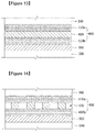
- Figs. 13 and 14 are sectional views of light emitting devices according to embodiments of the present invention.
- the transparent oxide layer 400 includes an intermediate dielectric layer 420 between upper and lower transparent conductive oxide layers 410a and 410b.
- the intermediate dielectric layer 420 is formed of an oxide such as SiO 2 , TiO 2 .
- the intermediate dielectric layer 430 formed of the oxide constitutes a specific pattern.
- This specific pattern can be identical or similar to the above-mentioned photonic crystal pattern. Space between the intermediate layer patterns can be filled with a transparent conductive oxide or remains empty.
- the photonic crystal 200 when the photonic crystal 200 can be introduced in the n-type semiconductor layer 110 of the vertical GaN light emitting device in order to improve external light extraction efficiency, by utilizing an interference effect and an etching depth of the reflective electrode 300, the maximum extraction efficiency can be accomplished in the photonic crystal 200 of a easily manufactured long period (more than 1 ⁇ m). Additionally, only using the interference effect of the reflective layer 300, extraction efficiency can be improved.
- the light emitting device can obtain high extraction efficiency regardless of the package structure.
Landscapes
- Led Devices (AREA)
- Electroluminescent Light Sources (AREA)
Applications Claiming Priority (2)
| Application Number | Priority Date | Filing Date | Title |
|---|---|---|---|
| KR1020080006073A KR101459764B1 (ko) | 2008-01-21 | 2008-01-21 | 질화물계 발광 소자 |
| PCT/KR2009/000318 WO2009093845A2 (ko) | 2008-01-21 | 2009-01-21 | 발광소자 |
Publications (3)
| Publication Number | Publication Date |
|---|---|
| EP2237332A2 EP2237332A2 (en) | 2010-10-06 |
| EP2237332A4 EP2237332A4 (en) | 2011-11-30 |
| EP2237332B1 true EP2237332B1 (en) | 2019-08-21 |
Family
ID=40901544
Family Applications (1)
| Application Number | Title | Priority Date | Filing Date |
|---|---|---|---|
| EP09704913.4A Active EP2237332B1 (en) | 2008-01-21 | 2009-01-21 | Light emitting device |
Country Status (6)
| Country | Link |
|---|---|
| US (2) | US8174040B2 (enExample) |
| EP (1) | EP2237332B1 (enExample) |
| JP (1) | JP5888854B2 (enExample) |
| KR (1) | KR101459764B1 (enExample) |
| CN (1) | CN101926011B (enExample) |
| WO (1) | WO2009093845A2 (enExample) |
Families Citing this family (19)
| Publication number | Priority date | Publication date | Assignee | Title |
|---|---|---|---|---|
| KR100736623B1 (ko) | 2006-05-08 | 2007-07-09 | 엘지전자 주식회사 | 수직형 발광 소자 및 그 제조방법 |
| KR101100681B1 (ko) * | 2009-09-10 | 2012-01-03 | 주식회사 에피밸리 | 반도체 발광소자 |
| KR101007077B1 (ko) | 2009-11-06 | 2011-01-10 | 엘지이노텍 주식회사 | 발광소자, 발광소자 패키지 및 그 제조방법 |
| KR101712094B1 (ko) * | 2009-11-27 | 2017-03-03 | 포항공과대학교 산학협력단 | 질화물갈륨계 수직 발광다이오드 및 그 제조 방법 |
| KR100993094B1 (ko) | 2010-02-01 | 2010-11-08 | 엘지이노텍 주식회사 | 발광소자 및 발광소자 패키지 |
| KR101028250B1 (ko) * | 2010-02-25 | 2011-04-11 | 엘지이노텍 주식회사 | 발광 소자 및 이를 이용한 발광 소자 패키지 |
| KR100999771B1 (ko) * | 2010-02-25 | 2010-12-08 | 엘지이노텍 주식회사 | 발광 소자, 발광 소자 제조방법 및 발광 소자 패키지 |
| KR101028220B1 (ko) * | 2010-02-25 | 2011-04-11 | 엘지이노텍 주식회사 | 발광 소자, 발광 소자 제조방법 및 발광 소자 패키지 |
| US8084776B2 (en) * | 2010-02-25 | 2011-12-27 | Lg Innotek Co., Ltd. | Light emitting device, light emitting device package, and lighting system |
| KR101047720B1 (ko) * | 2010-04-23 | 2011-07-08 | 엘지이노텍 주식회사 | 발광 소자, 발광 소자 제조방법 및 발광 소자 패키지 |
| KR101701510B1 (ko) | 2010-07-09 | 2017-02-01 | 엘지이노텍 주식회사 | 발광소자 |
| JP2014103240A (ja) * | 2012-11-20 | 2014-06-05 | Stanley Electric Co Ltd | 半導体発光素子 |
| JP6190585B2 (ja) * | 2012-12-12 | 2017-08-30 | スタンレー電気株式会社 | 多重量子井戸半導体発光素子 |
| EP2968684A1 (en) * | 2013-03-15 | 2016-01-20 | Abbott Cardiovascular Systems Inc. | Crosslinked coatings delivered via a balloon |
| KR101521081B1 (ko) * | 2013-10-01 | 2015-05-18 | 경희대학교 산학협력단 | 발광 다이오드 패키지 |
| JP6826395B2 (ja) * | 2016-08-26 | 2021-02-03 | ローム株式会社 | 半導体発光素子 |
| KR102555005B1 (ko) * | 2016-11-24 | 2023-07-14 | 삼성전자주식회사 | 반도체 발광 소자 및 반도체 발광 소자의 제조 방법 |
| JP7316610B6 (ja) * | 2018-01-26 | 2024-02-19 | 丸文株式会社 | 深紫外led及びその製造方法 |
| JP2022172792A (ja) * | 2021-05-07 | 2022-11-17 | 日機装株式会社 | 窒化物半導体発光素子 |
Family Cites Families (19)
| Publication number | Priority date | Publication date | Assignee | Title |
|---|---|---|---|---|
| DE69124338T2 (de) | 1990-11-02 | 1997-07-31 | Daido Steel Co Ltd | Halbleitervorrichtung mit reflektierender Schicht |
| JP3134382B2 (ja) * | 1991-07-31 | 2001-02-13 | 大同特殊鋼株式会社 | チャープ状光反射層を備えた半導体装置 |
| JPH0527177A (ja) * | 1991-07-25 | 1993-02-05 | Fuji Photo Film Co Ltd | 走査型顕微鏡 |
| GB2353400B (en) | 1999-08-20 | 2004-01-14 | Cambridge Display Tech Ltd | Mutiple-wavelength light emitting device and electronic apparatus |
| US6486499B1 (en) * | 1999-12-22 | 2002-11-26 | Lumileds Lighting U.S., Llc | III-nitride light-emitting device with increased light generating capability |
| US6784462B2 (en) * | 2001-12-13 | 2004-08-31 | Rensselaer Polytechnic Institute | Light-emitting diode with planar omni-directional reflector |
| JP2004056010A (ja) * | 2002-07-23 | 2004-02-19 | Toyota Central Res & Dev Lab Inc | 窒化物半導体発光素子 |
| JP4350996B2 (ja) * | 2002-11-26 | 2009-10-28 | 日東電工株式会社 | 有機エレクトロルミネッセンス素子、面光源および表示装置 |
| TWI312582B (en) * | 2003-07-24 | 2009-07-21 | Epistar Corporatio | Led device, flip-chip led package and light reflecting structure |
| JP4315760B2 (ja) * | 2003-07-31 | 2009-08-19 | 株式会社沖データ | 半導体発光装置、ledヘッド、画像形成装置、及び半導体発光装置の製造方法 |
| US7119372B2 (en) * | 2003-10-24 | 2006-10-10 | Gelcore, Llc | Flip-chip light emitting diode |
| DE102005016592A1 (de) | 2004-04-14 | 2005-11-24 | Osram Opto Semiconductors Gmbh | Leuchtdiodenchip |
| TWI292631B (en) * | 2005-02-05 | 2008-01-11 | Epistar Corp | Light emitting diode and method of the same |
| US20070018182A1 (en) * | 2005-07-20 | 2007-01-25 | Goldeneye, Inc. | Light emitting diodes with improved light extraction and reflectivity |
| EP2005488B1 (en) * | 2005-12-16 | 2013-07-31 | Samsung Display Co., Ltd. | Optical device and method of fabricating the same |
| KR100862505B1 (ko) * | 2006-02-01 | 2008-10-08 | 삼성전기주식회사 | 발광 다이오드 소자 및 그 제조방법 |
| KR100736623B1 (ko) * | 2006-05-08 | 2007-07-09 | 엘지전자 주식회사 | 수직형 발광 소자 및 그 제조방법 |
| TWI370560B (en) * | 2007-12-14 | 2012-08-11 | Delta Electronics Inc | Light-emitting diode device and manufacturing method thereof |
| US8143636B2 (en) * | 2008-11-18 | 2012-03-27 | Epistar Corporation | Light-emitting device |
-
2008
- 2008-01-21 KR KR1020080006073A patent/KR101459764B1/ko not_active Expired - Fee Related
-
2009
- 2009-01-21 EP EP09704913.4A patent/EP2237332B1/en active Active
- 2009-01-21 CN CN200980102755XA patent/CN101926011B/zh active Active
- 2009-01-21 JP JP2010544223A patent/JP5888854B2/ja not_active Expired - Fee Related
- 2009-01-21 WO PCT/KR2009/000318 patent/WO2009093845A2/ko not_active Ceased
- 2009-01-21 US US12/514,615 patent/US8174040B2/en active Active
-
2012
- 2012-04-17 US US13/449,097 patent/US20120199864A1/en not_active Abandoned
Non-Patent Citations (1)
| Title |
|---|
| None * |
Also Published As
| Publication number | Publication date |
|---|---|
| EP2237332A2 (en) | 2010-10-06 |
| CN101926011B (zh) | 2013-01-23 |
| CN101926011A (zh) | 2010-12-22 |
| JP5888854B2 (ja) | 2016-03-22 |
| WO2009093845A3 (ko) | 2009-10-22 |
| US8174040B2 (en) | 2012-05-08 |
| US20120199864A1 (en) | 2012-08-09 |
| WO2009093845A2 (ko) | 2009-07-30 |
| JP2011510512A (ja) | 2011-03-31 |
| KR101459764B1 (ko) | 2014-11-12 |
| US20100314645A1 (en) | 2010-12-16 |
| EP2237332A4 (en) | 2011-11-30 |
| KR20090080218A (ko) | 2009-07-24 |
Similar Documents
| Publication | Publication Date | Title |
|---|---|---|
| EP2237332B1 (en) | Light emitting device | |
| EP2056368B1 (en) | Light emitting device and method for manufacturing the same | |
| RU2491682C2 (ru) | Полупроводниковое светоизлучающее устройство со структурами вывода света | |
| EP2362440A2 (en) | Semiconductor light emitting device | |
| CN101257077B (zh) | 具有光子晶体高反射层的半导体发光二极管器件 | |
| KR20070081184A (ko) | 질화물계 반도체 발광소자 및 그 제조방법 | |
| US20050161696A1 (en) | Semiconductor light-emitting device and method for fabricating the same | |
| KR20230119152A (ko) | 축형 3차원 발광다이오드를 갖는 광전자 장치 | |
| JP2012191208A (ja) | 広い視野角を有する発光ダイオードとその製造方法 | |
| US8340146B2 (en) | Radiation-emitting semiconductor chip | |
| KR20120102137A (ko) | 광전자 반도체 칩 | |
| KR20080093558A (ko) | 질화물계 발광 소자 | |
| KR20090074359A (ko) | 적색 발광 소자 및 그 제조방법 | |
| KR100921462B1 (ko) | 수직형 발광 소자 | |
| CN104160518A (zh) | 用于具有较高光提取率的led的结构化基底 | |
| KR20080093557A (ko) | 질화물계 발광 소자 | |
| JP7738851B2 (ja) | 発光ダイオード素子 | |
| EP4476800B1 (en) | Laser diode component | |
| CN116364823B (zh) | 一种GaN基纳米多孔结构Micro-LED器件 | |
| TW201013993A (en) | Optoelectronic semiconductor chip and method for its manufacture | |
| Fu et al. | Lattice constant effects of photonic crystals on the extraction of guided mode of GaN based light emitting diodes | |
| KR101106340B1 (ko) | Led 소자의 구조 및 제조방법 | |
| KR20070101421A (ko) | 발광 다이오드 | |
| KR100834033B1 (ko) | 질화물계 반도체 발광소자 및 그 제조방법 |
Legal Events
| Date | Code | Title | Description |
|---|---|---|---|
| PUAI | Public reference made under article 153(3) epc to a published international application that has entered the european phase |
Free format text: ORIGINAL CODE: 0009012 |
|
| 17P | Request for examination filed |
Effective date: 20100722 |
|
| AK | Designated contracting states |
Kind code of ref document: A2 Designated state(s): AT BE BG CH CY CZ DE DK EE ES FI FR GB GR HR HU IE IS IT LI LT LU LV MC MK MT NL NO PL PT RO SE SI SK TR |
|
| AX | Request for extension of the european patent |
Extension state: AL BA RS |
|
| DAX | Request for extension of the european patent (deleted) | ||
| A4 | Supplementary search report drawn up and despatched |
Effective date: 20111031 |
|
| RIC1 | Information provided on ipc code assigned before grant |
Ipc: H01L 33/46 20100101ALN20111025BHEP Ipc: H01L 33/20 20100101ALN20111025BHEP Ipc: H01L 33/42 20100101AFI20111025BHEP |
|
| 17Q | First examination report despatched |
Effective date: 20121009 |
|
| RAP1 | Party data changed (applicant data changed or rights of an application transferred) |
Owner name: LG INNOTEK CO., LTD. |
|
| RAP1 | Party data changed (applicant data changed or rights of an application transferred) |
Owner name: LG INNOTEK CO., LTD. |
|
| STAA | Information on the status of an ep patent application or granted ep patent |
Free format text: STATUS: EXAMINATION IS IN PROGRESS |
|
| REG | Reference to a national code |
Ref country code: DE Ref legal event code: R079 Ref document number: 602009059532 Country of ref document: DE Free format text: PREVIOUS MAIN CLASS: H01L0033000000 Ipc: H01L0033420000 |
|
| GRAP | Despatch of communication of intention to grant a patent |
Free format text: ORIGINAL CODE: EPIDOSNIGR1 |
|
| STAA | Information on the status of an ep patent application or granted ep patent |
Free format text: STATUS: GRANT OF PATENT IS INTENDED |
|
| RIC1 | Information provided on ipc code assigned before grant |
Ipc: H01L 33/40 20100101ALN20190206BHEP Ipc: H01L 33/42 20100101AFI20190206BHEP Ipc: H01L 33/44 20100101ALI20190206BHEP Ipc: H01L 33/32 20100101ALN20190206BHEP Ipc: H01L 33/20 20100101ALN20190206BHEP Ipc: H01L 33/00 20100101ALN20190206BHEP Ipc: H01L 33/46 20100101ALN20190206BHEP |
|
| INTG | Intention to grant announced |
Effective date: 20190312 |
|
| GRAS | Grant fee paid |
Free format text: ORIGINAL CODE: EPIDOSNIGR3 |
|
| GRAA | (expected) grant |
Free format text: ORIGINAL CODE: 0009210 |
|
| STAA | Information on the status of an ep patent application or granted ep patent |
Free format text: STATUS: THE PATENT HAS BEEN GRANTED |
|
| AK | Designated contracting states |
Kind code of ref document: B1 Designated state(s): AT BE BG CH CY CZ DE DK EE ES FI FR GB GR HR HU IE IS IT LI LT LU LV MC MK MT NL NO PL PT RO SE SI SK TR |
|
| REG | Reference to a national code |
Ref country code: GB Ref legal event code: FG4D |
|
| REG | Reference to a national code |
Ref country code: CH Ref legal event code: EP |
|
| REG | Reference to a national code |
Ref country code: DE Ref legal event code: R096 Ref document number: 602009059532 Country of ref document: DE |
|
| REG | Reference to a national code |
Ref country code: AT Ref legal event code: REF Ref document number: 1170746 Country of ref document: AT Kind code of ref document: T Effective date: 20190915 |
|
| REG | Reference to a national code |
Ref country code: IE Ref legal event code: FG4D |
|
| REG | Reference to a national code |
Ref country code: NL Ref legal event code: FP |
|
| REG | Reference to a national code |
Ref country code: LT Ref legal event code: MG4D |
|
| PG25 | Lapsed in a contracting state [announced via postgrant information from national office to epo] |
Ref country code: PT Free format text: LAPSE BECAUSE OF FAILURE TO SUBMIT A TRANSLATION OF THE DESCRIPTION OR TO PAY THE FEE WITHIN THE PRESCRIBED TIME-LIMIT Effective date: 20191223 Ref country code: BG Free format text: LAPSE BECAUSE OF FAILURE TO SUBMIT A TRANSLATION OF THE DESCRIPTION OR TO PAY THE FEE WITHIN THE PRESCRIBED TIME-LIMIT Effective date: 20191121 Ref country code: HR Free format text: LAPSE BECAUSE OF FAILURE TO SUBMIT A TRANSLATION OF THE DESCRIPTION OR TO PAY THE FEE WITHIN THE PRESCRIBED TIME-LIMIT Effective date: 20190821 Ref country code: LT Free format text: LAPSE BECAUSE OF FAILURE TO SUBMIT A TRANSLATION OF THE DESCRIPTION OR TO PAY THE FEE WITHIN THE PRESCRIBED TIME-LIMIT Effective date: 20190821 Ref country code: NO Free format text: LAPSE BECAUSE OF FAILURE TO SUBMIT A TRANSLATION OF THE DESCRIPTION OR TO PAY THE FEE WITHIN THE PRESCRIBED TIME-LIMIT Effective date: 20191121 Ref country code: FI Free format text: LAPSE BECAUSE OF FAILURE TO SUBMIT A TRANSLATION OF THE DESCRIPTION OR TO PAY THE FEE WITHIN THE PRESCRIBED TIME-LIMIT Effective date: 20190821 Ref country code: SE Free format text: LAPSE BECAUSE OF FAILURE TO SUBMIT A TRANSLATION OF THE DESCRIPTION OR TO PAY THE FEE WITHIN THE PRESCRIBED TIME-LIMIT Effective date: 20190821 |
|
| PG25 | Lapsed in a contracting state [announced via postgrant information from national office to epo] |
Ref country code: GR Free format text: LAPSE BECAUSE OF FAILURE TO SUBMIT A TRANSLATION OF THE DESCRIPTION OR TO PAY THE FEE WITHIN THE PRESCRIBED TIME-LIMIT Effective date: 20191122 Ref country code: IS Free format text: LAPSE BECAUSE OF FAILURE TO SUBMIT A TRANSLATION OF THE DESCRIPTION OR TO PAY THE FEE WITHIN THE PRESCRIBED TIME-LIMIT Effective date: 20191221 Ref country code: ES Free format text: LAPSE BECAUSE OF FAILURE TO SUBMIT A TRANSLATION OF THE DESCRIPTION OR TO PAY THE FEE WITHIN THE PRESCRIBED TIME-LIMIT Effective date: 20190821 Ref country code: LV Free format text: LAPSE BECAUSE OF FAILURE TO SUBMIT A TRANSLATION OF THE DESCRIPTION OR TO PAY THE FEE WITHIN THE PRESCRIBED TIME-LIMIT Effective date: 20190821 |
|
| REG | Reference to a national code |
Ref country code: AT Ref legal event code: MK05 Ref document number: 1170746 Country of ref document: AT Kind code of ref document: T Effective date: 20190821 |
|
| PG25 | Lapsed in a contracting state [announced via postgrant information from national office to epo] |
Ref country code: TR Free format text: LAPSE BECAUSE OF FAILURE TO SUBMIT A TRANSLATION OF THE DESCRIPTION OR TO PAY THE FEE WITHIN THE PRESCRIBED TIME-LIMIT Effective date: 20190821 |
|
| PG25 | Lapsed in a contracting state [announced via postgrant information from national office to epo] |
Ref country code: IT Free format text: LAPSE BECAUSE OF FAILURE TO SUBMIT A TRANSLATION OF THE DESCRIPTION OR TO PAY THE FEE WITHIN THE PRESCRIBED TIME-LIMIT Effective date: 20190821 Ref country code: RO Free format text: LAPSE BECAUSE OF FAILURE TO SUBMIT A TRANSLATION OF THE DESCRIPTION OR TO PAY THE FEE WITHIN THE PRESCRIBED TIME-LIMIT Effective date: 20190821 Ref country code: EE Free format text: LAPSE BECAUSE OF FAILURE TO SUBMIT A TRANSLATION OF THE DESCRIPTION OR TO PAY THE FEE WITHIN THE PRESCRIBED TIME-LIMIT Effective date: 20190821 Ref country code: DK Free format text: LAPSE BECAUSE OF FAILURE TO SUBMIT A TRANSLATION OF THE DESCRIPTION OR TO PAY THE FEE WITHIN THE PRESCRIBED TIME-LIMIT Effective date: 20190821 Ref country code: AT Free format text: LAPSE BECAUSE OF FAILURE TO SUBMIT A TRANSLATION OF THE DESCRIPTION OR TO PAY THE FEE WITHIN THE PRESCRIBED TIME-LIMIT Effective date: 20190821 Ref country code: PL Free format text: LAPSE BECAUSE OF FAILURE TO SUBMIT A TRANSLATION OF THE DESCRIPTION OR TO PAY THE FEE WITHIN THE PRESCRIBED TIME-LIMIT Effective date: 20190821 |
|
| PG25 | Lapsed in a contracting state [announced via postgrant information from national office to epo] |
Ref country code: CZ Free format text: LAPSE BECAUSE OF FAILURE TO SUBMIT A TRANSLATION OF THE DESCRIPTION OR TO PAY THE FEE WITHIN THE PRESCRIBED TIME-LIMIT Effective date: 20190821 Ref country code: SK Free format text: LAPSE BECAUSE OF FAILURE TO SUBMIT A TRANSLATION OF THE DESCRIPTION OR TO PAY THE FEE WITHIN THE PRESCRIBED TIME-LIMIT Effective date: 20190821 Ref country code: IS Free format text: LAPSE BECAUSE OF FAILURE TO SUBMIT A TRANSLATION OF THE DESCRIPTION OR TO PAY THE FEE WITHIN THE PRESCRIBED TIME-LIMIT Effective date: 20200224 |
|
| REG | Reference to a national code |
Ref country code: DE Ref legal event code: R097 Ref document number: 602009059532 Country of ref document: DE |
|
| PLBE | No opposition filed within time limit |
Free format text: ORIGINAL CODE: 0009261 |
|
| STAA | Information on the status of an ep patent application or granted ep patent |
Free format text: STATUS: NO OPPOSITION FILED WITHIN TIME LIMIT |
|
| PG2D | Information on lapse in contracting state deleted |
Ref country code: IS |
|
| 26N | No opposition filed |
Effective date: 20200603 |
|
| PG25 | Lapsed in a contracting state [announced via postgrant information from national office to epo] |
Ref country code: MC Free format text: LAPSE BECAUSE OF FAILURE TO SUBMIT A TRANSLATION OF THE DESCRIPTION OR TO PAY THE FEE WITHIN THE PRESCRIBED TIME-LIMIT Effective date: 20190821 Ref country code: SI Free format text: LAPSE BECAUSE OF FAILURE TO SUBMIT A TRANSLATION OF THE DESCRIPTION OR TO PAY THE FEE WITHIN THE PRESCRIBED TIME-LIMIT Effective date: 20190821 |
|
| REG | Reference to a national code |
Ref country code: CH Ref legal event code: PL |
|
| GBPC | Gb: european patent ceased through non-payment of renewal fee |
Effective date: 20200121 |
|
| REG | Reference to a national code |
Ref country code: BE Ref legal event code: MM Effective date: 20200131 |
|
| PG25 | Lapsed in a contracting state [announced via postgrant information from national office to epo] |
Ref country code: FR Free format text: LAPSE BECAUSE OF NON-PAYMENT OF DUE FEES Effective date: 20200131 Ref country code: GB Free format text: LAPSE BECAUSE OF NON-PAYMENT OF DUE FEES Effective date: 20200121 Ref country code: LU Free format text: LAPSE BECAUSE OF NON-PAYMENT OF DUE FEES Effective date: 20200121 |
|
| PG25 | Lapsed in a contracting state [announced via postgrant information from national office to epo] |
Ref country code: BE Free format text: LAPSE BECAUSE OF NON-PAYMENT OF DUE FEES Effective date: 20200131 Ref country code: LI Free format text: LAPSE BECAUSE OF NON-PAYMENT OF DUE FEES Effective date: 20200131 Ref country code: CH Free format text: LAPSE BECAUSE OF NON-PAYMENT OF DUE FEES Effective date: 20200131 |
|
| PG25 | Lapsed in a contracting state [announced via postgrant information from national office to epo] |
Ref country code: IE Free format text: LAPSE BECAUSE OF NON-PAYMENT OF DUE FEES Effective date: 20200121 |
|
| REG | Reference to a national code |
Ref country code: NL Ref legal event code: PD Owner name: SUZHOU LEKIN SEMICONDUCTOR CO., LTD.; CN Free format text: DETAILS ASSIGNMENT: CHANGE OF OWNER(S), ASSIGNMENT; FORMER OWNER NAME: LG INNOTEK CO., LTD. Effective date: 20210719 |
|
| REG | Reference to a national code |
Ref country code: DE Ref legal event code: R081 Ref document number: 602009059532 Country of ref document: DE Owner name: SUZHOU LEKIN SEMICONDUCTOR CO. LTD., TAICANG, CN Free format text: FORMER OWNER: LG INNOTEK CO., LTD., SEOUL, KR |
|
| PG25 | Lapsed in a contracting state [announced via postgrant information from national office to epo] |
Ref country code: MT Free format text: LAPSE BECAUSE OF FAILURE TO SUBMIT A TRANSLATION OF THE DESCRIPTION OR TO PAY THE FEE WITHIN THE PRESCRIBED TIME-LIMIT Effective date: 20190821 Ref country code: CY Free format text: LAPSE BECAUSE OF FAILURE TO SUBMIT A TRANSLATION OF THE DESCRIPTION OR TO PAY THE FEE WITHIN THE PRESCRIBED TIME-LIMIT Effective date: 20190821 |
|
| PG25 | Lapsed in a contracting state [announced via postgrant information from national office to epo] |
Ref country code: MK Free format text: LAPSE BECAUSE OF FAILURE TO SUBMIT A TRANSLATION OF THE DESCRIPTION OR TO PAY THE FEE WITHIN THE PRESCRIBED TIME-LIMIT Effective date: 20190821 |
|
| PGFP | Annual fee paid to national office [announced via postgrant information from national office to epo] |
Ref country code: NL Payment date: 20221220 Year of fee payment: 15 |
|
| REG | Reference to a national code |
Ref country code: NL Ref legal event code: MM Effective date: 20240201 |
|
| PG25 | Lapsed in a contracting state [announced via postgrant information from national office to epo] |
Ref country code: NL Free format text: LAPSE BECAUSE OF NON-PAYMENT OF DUE FEES Effective date: 20240201 |
|
| PG25 | Lapsed in a contracting state [announced via postgrant information from national office to epo] |
Ref country code: NL Free format text: LAPSE BECAUSE OF NON-PAYMENT OF DUE FEES Effective date: 20240201 |
|
| REG | Reference to a national code |
Ref country code: DE Ref legal event code: R079 Ref document number: 602009059532 Country of ref document: DE Free format text: PREVIOUS MAIN CLASS: H01L0033420000 Ipc: H10H0020833000 |
|
| PGFP | Annual fee paid to national office [announced via postgrant information from national office to epo] |
Ref country code: DE Payment date: 20241203 Year of fee payment: 17 |