EP2235751B1 - Flexible kontaktfreie drahtbondstruktur und verfahren für halbleiterbauelement - Google Patents
Flexible kontaktfreie drahtbondstruktur und verfahren für halbleiterbauelement Download PDFInfo
- Publication number
- EP2235751B1 EP2235751B1 EP08870490.3A EP08870490A EP2235751B1 EP 2235751 B1 EP2235751 B1 EP 2235751B1 EP 08870490 A EP08870490 A EP 08870490A EP 2235751 B1 EP2235751 B1 EP 2235751B1
- Authority
- EP
- European Patent Office
- Prior art keywords
- leads
- die
- semiconductor device
- layer
- wires
- Prior art date
- Legal status (The legal status is an assumption and is not a legal conclusion. Google has not performed a legal analysis and makes no representation as to the accuracy of the status listed.)
- Not-in-force
Links
Images


Classifications
-
- H—ELECTRICITY
- H10—SEMICONDUCTOR DEVICES; ELECTRIC SOLID-STATE DEVICES NOT OTHERWISE PROVIDED FOR
- H10W—GENERIC PACKAGES, INTERCONNECTIONS, CONNECTORS OR OTHER CONSTRUCTIONAL DETAILS OF DEVICES COVERED BY CLASS H10
- H10W70/00—Package substrates; Interposers; Redistribution layers [RDL]
- H10W70/40—Leadframes
- H10W70/481—Leadframes for devices being provided for in groups H10D8/00 - H10D48/00
-
- H—ELECTRICITY
- H10—SEMICONDUCTOR DEVICES; ELECTRIC SOLID-STATE DEVICES NOT OTHERWISE PROVIDED FOR
- H10W—GENERIC PACKAGES, INTERCONNECTIONS, CONNECTORS OR OTHER CONSTRUCTIONAL DETAILS OF DEVICES COVERED BY CLASS H10
- H10W70/00—Package substrates; Interposers; Redistribution layers [RDL]
- H10W70/40—Leadframes
- H10W70/464—Additional interconnections in combination with leadframes
- H10W70/465—Bumps or wires
-
- H—ELECTRICITY
- H10—SEMICONDUCTOR DEVICES; ELECTRIC SOLID-STATE DEVICES NOT OTHERWISE PROVIDED FOR
- H10W—GENERIC PACKAGES, INTERCONNECTIONS, CONNECTORS OR OTHER CONSTRUCTIONAL DETAILS OF DEVICES COVERED BY CLASS H10
- H10W72/00—Interconnections or connectors in packages
- H10W72/071—Connecting or disconnecting
- H10W72/075—Connecting or disconnecting of bond wires
- H10W72/07551—Connecting or disconnecting of bond wires characterised by changes in properties of the bond wires during the connecting
- H10W72/07554—Connecting or disconnecting of bond wires characterised by changes in properties of the bond wires during the connecting changes in dispositions
-
- H—ELECTRICITY
- H10—SEMICONDUCTOR DEVICES; ELECTRIC SOLID-STATE DEVICES NOT OTHERWISE PROVIDED FOR
- H10W—GENERIC PACKAGES, INTERCONNECTIONS, CONNECTORS OR OTHER CONSTRUCTIONAL DETAILS OF DEVICES COVERED BY CLASS H10
- H10W72/00—Interconnections or connectors in packages
- H10W72/50—Bond wires
- H10W72/531—Shapes of wire connectors
- H10W72/536—Shapes of wire connectors the connected ends being ball-shaped
-
- H—ELECTRICITY
- H10—SEMICONDUCTOR DEVICES; ELECTRIC SOLID-STATE DEVICES NOT OTHERWISE PROVIDED FOR
- H10W—GENERIC PACKAGES, INTERCONNECTIONS, CONNECTORS OR OTHER CONSTRUCTIONAL DETAILS OF DEVICES COVERED BY CLASS H10
- H10W72/00—Interconnections or connectors in packages
- H10W72/50—Bond wires
- H10W72/531—Shapes of wire connectors
- H10W72/5363—Shapes of wire connectors the connected ends being wedge-shaped
-
- H—ELECTRICITY
- H10—SEMICONDUCTOR DEVICES; ELECTRIC SOLID-STATE DEVICES NOT OTHERWISE PROVIDED FOR
- H10W—GENERIC PACKAGES, INTERCONNECTIONS, CONNECTORS OR OTHER CONSTRUCTIONAL DETAILS OF DEVICES COVERED BY CLASS H10
- H10W72/00—Interconnections or connectors in packages
- H10W72/50—Bond wires
- H10W72/531—Shapes of wire connectors
- H10W72/5366—Shapes of wire connectors the bond wires having kinks
-
- H—ELECTRICITY
- H10—SEMICONDUCTOR DEVICES; ELECTRIC SOLID-STATE DEVICES NOT OTHERWISE PROVIDED FOR
- H10W—GENERIC PACKAGES, INTERCONNECTIONS, CONNECTORS OR OTHER CONSTRUCTIONAL DETAILS OF DEVICES COVERED BY CLASS H10
- H10W72/00—Interconnections or connectors in packages
- H10W72/50—Bond wires
- H10W72/541—Dispositions of bond wires
- H10W72/547—Dispositions of multiple bond wires
-
- H—ELECTRICITY
- H10—SEMICONDUCTOR DEVICES; ELECTRIC SOLID-STATE DEVICES NOT OTHERWISE PROVIDED FOR
- H10W—GENERIC PACKAGES, INTERCONNECTIONS, CONNECTORS OR OTHER CONSTRUCTIONAL DETAILS OF DEVICES COVERED BY CLASS H10
- H10W72/00—Interconnections or connectors in packages
- H10W72/50—Bond wires
- H10W72/551—Materials of bond wires
- H10W72/552—Materials of bond wires comprising metals or metalloids, e.g. silver
- H10W72/5522—Materials of bond wires comprising metals or metalloids, e.g. silver comprising gold [Au]
-
- H—ELECTRICITY
- H10—SEMICONDUCTOR DEVICES; ELECTRIC SOLID-STATE DEVICES NOT OTHERWISE PROVIDED FOR
- H10W—GENERIC PACKAGES, INTERCONNECTIONS, CONNECTORS OR OTHER CONSTRUCTIONAL DETAILS OF DEVICES COVERED BY CLASS H10
- H10W72/00—Interconnections or connectors in packages
- H10W72/50—Bond wires
- H10W72/551—Materials of bond wires
- H10W72/552—Materials of bond wires comprising metals or metalloids, e.g. silver
- H10W72/5525—Materials of bond wires comprising metals or metalloids, e.g. silver comprising copper [Cu]
-
- H—ELECTRICITY
- H10—SEMICONDUCTOR DEVICES; ELECTRIC SOLID-STATE DEVICES NOT OTHERWISE PROVIDED FOR
- H10W—GENERIC PACKAGES, INTERCONNECTIONS, CONNECTORS OR OTHER CONSTRUCTIONAL DETAILS OF DEVICES COVERED BY CLASS H10
- H10W72/00—Interconnections or connectors in packages
- H10W72/50—Bond wires
- H10W72/59—Bond pads specially adapted therefor
-
- H—ELECTRICITY
- H10—SEMICONDUCTOR DEVICES; ELECTRIC SOLID-STATE DEVICES NOT OTHERWISE PROVIDED FOR
- H10W—GENERIC PACKAGES, INTERCONNECTIONS, CONNECTORS OR OTHER CONSTRUCTIONAL DETAILS OF DEVICES COVERED BY CLASS H10
- H10W72/00—Interconnections or connectors in packages
- H10W72/90—Bond pads, in general
- H10W72/951—Materials of bond pads
- H10W72/952—Materials of bond pads comprising metals or metalloids, e.g. PbSn, Ag or Cu
-
- H—ELECTRICITY
- H10—SEMICONDUCTOR DEVICES; ELECTRIC SOLID-STATE DEVICES NOT OTHERWISE PROVIDED FOR
- H10W—GENERIC PACKAGES, INTERCONNECTIONS, CONNECTORS OR OTHER CONSTRUCTIONAL DETAILS OF DEVICES COVERED BY CLASS H10
- H10W74/00—Encapsulations, e.g. protective coatings
-
- H—ELECTRICITY
- H10—SEMICONDUCTOR DEVICES; ELECTRIC SOLID-STATE DEVICES NOT OTHERWISE PROVIDED FOR
- H10W—GENERIC PACKAGES, INTERCONNECTIONS, CONNECTORS OR OTHER CONSTRUCTIONAL DETAILS OF DEVICES COVERED BY CLASS H10
- H10W90/00—Package configurations
- H10W90/701—Package configurations characterised by the relative positions of pads or connectors relative to package parts
- H10W90/751—Package configurations characterised by the relative positions of pads or connectors relative to package parts of bond wires
- H10W90/756—Package configurations characterised by the relative positions of pads or connectors relative to package parts of bond wires between a chip and a stacked lead frame, conducting package substrate or heat sink
Definitions
- This disclosure relates generally to semiconductor device manufacture, such as a field-effect transistor, and more particularly to an improved structure for and methodology of wire bonding without direct contact to the die surface via wire bonding welds, and in which wire interconnect resistance is considerably reduced.
- a typical integrated circuit package includes a semiconductor die having an array of die output/input bond pads and some means, such as a leadframe, for supporting the die and providing leads for interconnecting the bond pads with external circuitry.
- the leadframe or support structure generally comprises a die paddle on which the die is positioned, and an array of laterally extending electrically conductive contacts or leads connected to corresponding die bond pads through cooperating bond wires.
- the die may contain a complex array of electrical components; in others the die may contain a single, or small number of larger components such as one or more field effect transistors that may be used for high power switching.
- bond wires generally gold, are ball bonded to an aluminized surface of the die that will form the source by a welding process in which vibration, pressure and heat are implemented to create a weld.
- the opposite ends of the bond wires are wedge bonded to the lead tips of the device.
- Fig. 1 shows an example of wire bonds arranged between a semiconductor die forming a field-effect transistor device 100 and an array of laterally extending leads that protrude from the package that will complete the device.
- the device 100 which in Fig. 1 is in an intermediate stage of fabrication, comprises a leadframe 102 which consists of a die paddle 104 supporting a semiconductor die 106, corner leads 108 at the four corners of and integral with the paddle, and a number of independent leads 110 that extend laterally, but are spaced apart, from the paddle. In Fig. 1 , six leads 110 are shown although the leads could be greater or fewer in number.
- the leadframe 102 further includes a tie bar 112 which, when encapsulated in a mold compound, helps to maintain the device 100 in stable assembly.
- An aluminum metallization layer 116 is formed on the upper surface of the die 106.
- the layer 116 may form a source electrode, and the die paddle on the undersurface of the die may form a drain electrode.
- a gate electrode 118 may be established through the metallization layer 116, as depicted.
- the drain electrode is connected to corner leads 108 through a layer of conductive paste which also secures die 106 to paddle 104.
- An electrical connection is established between the source electrode 116 and leads 110 through a multiplicity of gold or copper wires 120, which extend from points on the electrode to lead tip portions of the leads 110.
- a connection between a bonding wire and the surface layer is made using a welding tool to ball bond one end of a wire to the electrode, as at 120a, and wedge bonding the opposite end of the wire to a counterpart lead tip 110 (in this example, the lower left hand corner lead). This process can be repeated for each lead (in which there are twelve in Fig. 1 , six on each side of the lead frame).
- the wire ball bonds may be staggered on the surface of the metallization layer 116, as depicted, to distribute current in the source.
- a molding compound is now applied to encapsulate the die paddle, bond wires and leads. Thereafter, the leads are detached from the common connection with the lead frame 102, in a process known as "singulation.”
- the performance of a field-effect transistor is determined, in part, by the amount of electrical resistance that exists between leads 120 at the source electrode and corner leads 108 at the drain.
- the composite resistance that resides in the device is the sum of several resistance components: a first resistance component between a lead tip 110 and the source electrode 116 representing resistance of the wire and contact resistance between wire and lead tip, and wire and electrode; a second component comprising the resistance of the source layer 116; a third resistance comprising the resistance of die 106; and a fourth component comprising the resistance of the conductive paste between the die and die paddle 104 which is integral with leads 108.
- the composite resistance should be minimized to enable the field-effect transistor to conduct as much current as possible without substantial heating, and to realize other performance objectives.
- a multiplicity of wires can be connected between the source electrode and a common lead tip to reduce minimize resistance between the source electrode and the leads. For example, if two wires 120 are connected between each lead tip and the source electrode, the assembly will consist of twenty-four wire connections. Because two wires extend between the source electrode and each lead 110, the effective resistance of a connection between the electrode and each lead is reduced by one-half. However, using this technique, source electrode resistance remains unchanged and relatively substantial, and limits reduction in composite resistance that currently is practical. Improvement is desired.
- Document US 2006/017141 A1 discloses a semiconductor package including a relatively thick lead frame having a plurality of leads and a first lead frame pad, the first lead frame pad including a die coupled thereto, bonding wires connecting the die to the plurality of leads, the bonding wires being aluminium, and a resin body encapsulating the die, bonding wires and at least a portion of the lead frame.
- connection element arranged on a connection area of a semiconductor component.
- the connection element includes at least one bonding wire portion fixed on the connection area.
- the connection area is covered by an electrically conductive material, the fixed bonding wire portion being surrounded or embedded by the electrically conductive material.
- Document DE 10 2005 054 872 A1 discloses a device having an electrode contact surface and a control electrode surface provided on an upper side of the device. Platings are respectively arranged on the electrode contact surface and the control electrode surface. The thickness of the plating on the electrode contact surface is 10 times more than the thickness of the plating on the control electrode surface. A diffusion solder layer is arranged on the outer surface of the plating.
- At least one electrically conductive wire, and preferably plural wires, extend laterally across the upper surface of the semiconductor die, are in electrical contact with the conductive material, and interconnect corresponding leads of the second set of leads on opposite sides of the die.
- the plural wires may be welded to common leads by alternate ball and wedge bonds on each lead tip.
- the layer of electrically conductive material may be an aluminized layer on which is formed a thin layer of solderable material, such as tin, on which solder is deposited, enmeshed with the wires.
- the wires which preferably are made of copper, then may be bonded to the electrically conductive layer by melting the solder, preferably by heating the leadframe, to reflow the solder and wet the wires. The solder then is allowed to solidify.
- the semiconductor device may be a field-effect transistor, in which the conductive layer forms a source electrode, the die paddle forms a drain electrode, and a gate electrode is formed in the die, through the source electrode.
- Reduced resistance between leads and die as provided herein enables performance of the transistor to be considerably improved.
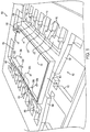
- FIG. 2 depicted is an integrated circuit assembly, in the exemplary form of a field-effect transistor 200, that is similar to that shown in FIG. 1 . However, the manner and structure with which leads 210 and the die 208 are interconnected has been improved.
- the device 200 which, as in Fig. 1 , is in an intermediate stage of fabrication, comprises lead frame 202 which includes a die paddle 204 supporting a semiconductor die 206, corner leads 208 at the four corners of, and integral with, the paddle, and independent leads 210 that extend laterally, but are separated from, the paddle. As in Fig. 1 , six leads 210 are shown in Fig. 2 , although the leads could be greater or fewer in number.
- the lead frame 202 further includes tie bar 212 which connects the die paddle 204 to the leadframe 202 (although shown in detached form in Fig. 2 ), and when encapsulated in a mold compound, helps to maintain the device 200 in stable assembly.
- An aluminum layer 216 is formed on the upper surface of the 206.
- the layer 216 may form a source electrode, and the undersurface of the die (on paddle 204) may form a drain electrode.
- a gate electrode 218 may be established through the metallization layer 216, as depicted.
- the drain electrode is connected to corner leads 208 through a layer of conductive paste, for example, solder, which also secures the die 206 to the die paddle 204.
- a difference between the transistor 100 of Fig. 1 and transistor 200 of Fig. 2 is in the wire interconnect structure which connects the source electrode 216 with leads 208.
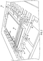
- the surface of aluminum layer 216, the source electrode is coated with a thin layer 224, see Fig. 3 , of solderable material, such as tin.
- At least one, but advantageously a plurality of wires 226, preferably made of copper, are connected between corresponding leads 210 of the leadframe 204, and straddle the die in contact with the source electrode 216 throughout most or all of the lateral extent of the electrode.
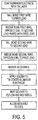
- the interconnect structure depicted in Figs. 2 and 3 is manufactured using a conventional wire bonding tool (not shown), in which the process (summarized by a flow chart in Fig. 5 ) begins with a ball bond at the left hand side, corner, lead tip 210a.
- the wire is now drawn tautly to the right in the figure, across and resting immediately above or upon the upper surface of the semiconductor die to terminate with a wedge bond at the right hand side, corner, lead tip 210b.
- a second wire 226 is next ball bonded to lead tip 210b adjacent and outboard of the wedge bond of the first wire, and is wedge bonded to lead tip 210a adjacent and inboard of the ball bond of the first wire, as depicted.
- This process may be repeated on additional wires any number of times using alternate ball and wedge bonds, as described, to form a multiplicity of wires arranged in parallel between a pair of leads, atop the die, and near or in contact with the source electrode 216.
- the described process of drawing and welding wires to corresponding leads on opposite sides of the die will preferably continue to be repeated a number of times for each pair of leads.
- six pairs of leads, with two pairs of wires spanning the die between one pair of the leads, are shown in the example of Fig. 2 .
- a greater number of such wires connected between leads of the device will create an interconnect of lesser composite resistance. Larger diameter wires similarly will reduce resistance, although wires of 2 mils in diameter are standard.
- the leads 210 may be oriented as shown to connect all wires in electrical parallel so as to create a low resistance path from the leads to the source electrode of the device.
- a layer 228 of solder is now deposited on the surface of source electrode 216 and wires 210 and then heated, preferably by heating the leadframe, to reflow the solder and wet the copper wires to create a conductive medium that spans a portion or substantially the entire surface of the source electrode.
- the solder now is allowed to cool, or is cooled, to cause the solder to solidify.
- the conductive medium that results is of nearly negligible resistance, leaving a residual resistance that resides substantially only between die and lead tips on each side of the device.
- Fig. 4 shows the device with conductive medium 228, now solidified, in which wires 226 are embedded.
- the assembly will be encapsulated and singulated, in a conventional manner, to produce the desired field-effect transistor or other semiconductor device.
- a semiconductor device such as a field-effect transistor, will have been manufactured, having considerably lower resistance than heretofore available, with associated increased current carrying capability and improvement in performance.
Landscapes
- Wire Bonding (AREA)
- Lead Frames For Integrated Circuits (AREA)
- Die Bonding (AREA)
Claims (13)
- Eine Halbleitervorrichtung (200), die Folgendes umfasst:einen Leiterrahmen (202), der einen Chipträger (204) umfasst, der einstückig mit einem ersten Satz von Zuleitungen bzw. Anschlussbeinen ist, und einen zweiten Satz von Zuleitungen (210), der vom ersten Satz an Zuleitungen elektrisch isoliert ist;einen Halbleiterchip (206), der eine erste Oberfläche aufweist, die auf dem Chipträger (204) angeordnet ist und damit elektrisch verbunden ist;eine Schicht aus leitendem Material (216) auf einer der ersten Oberfläche entgegengesetzten zweiten Oberfläche des Halbleiterchips (206);eine Vielzahl an elektrisch leitenden Drähten (226), die über der zweiten Oberfläche des Halbleiterchips (206) verlaufen, die mit der Schicht aus leitendem Material (216) im elektrischen Kontakt stehen, und die entsprechende Zuleitungen aus dem zweiten Satz von Zuleitungen (210) miteinander verbinden,wobei die Vielzahl an elektrisch leitenden Drähten (226) mit der Schicht aus leitendem Material (216) kontinuierlich in Kontakt stehen, überall in einem Bereich der Schicht (216) zwischen gegenüberliegenden Seiten des Halbleiterchips (206),dadurch gekennzeichnet, dassaneinander anliegende Drahtenden mit entsprechenden Zuleitungen aus dem zweiten Satz von Zuleitungen (210) entsprechend durch Ball- und Wedge-Bonds gebondet werden.
- Die Halbleitervorrichtung (200) nach Anspruch 1,
wobei die Halbleitervorrichtung (200) ein Feldeffekttransistor (200) ist,
wobei der Chipträger (204) eine Drain-Verbindung bildet;
wobei der zweite Satz von Zuleitungen (210) eine Source-Verbindung bildet;
wobei die Schicht aus leitendem Material (216) eine Source-Elektrode (216) bildet; und
wobei die Vielzahl an elektrisch leitenden Drähten (226), die über der zweiten Oberfläche des Halbleiterchips (206) verlaufen, die mit der Source-Elektrode (216) im elektrischen Kontakt stehen, und den entsprechenden zweiten Satz von Zuleitungen (210) an gegenüberliegenden Seiten des Chips (206) zusammenschalten. - Die Halbleitervorrichtung (200) nach Anspruch 1 oder 2, wobei die Vielzahl an elektrisch leitenden Drähten (226) mit der Schicht aus leitendem Material (216) mit einem Lötmaterial gebondet sind.
- Die Halbleitervorrichtung (200) nach Anspruch 1 oder 2, wobei mehrere Drähte (226) zwischen mindestens einem gegenüberliegenden Paar aus dem zweiten Satz von Zuleitungen (210) an gegenüberliegenden Seiten des Trägers (204) verlaufen.
- Die Halbleitervorrichtung (200) nach Anspruch 1, wobei die Schicht aus leitendem Material (216) aus mit Nickel beschichtetem Aluminium besteht.
- Die Halbleitervorrichtung (200) nach Anspruch 2, wobei die Source-Elektrode (216) aus einer mit Zinn beschichteten Aluminium-Schicht besteht.
- Die Halbleitervorrichtung (200) nach Anspruch 1 oder 2, wobei der Draht aus Kupfer hergestellt wird.
- Die Halbleitervorrichtung (200) nach Anspruch 1 oder 2, wobei der Chip (206) an den Chipträger (204) durch Lötmaterial oder Lötmittelpaste befestigt ist.
- Die Halbleitervorrichtung (200) nach Anspruch 1, wobei die Vorrichtung ein Feldeffekttransistor (200) ist, dessen erste Elektrode durch die erste Oberfläche des Halbleiterchips gebildet wird, dessen zweite Elektrode durch die Schicht aus leitendem Material (216) gebildet wird, und einer Gate-Elektrode (218).
- Der Feldeffekttransistor (200) nach Anspruch 2, wobei die Source-Elektrode (216) mit einer Schicht aus lötfähigem Material (224) beschichtet ist.
- Ein Verfahren zur Herstellung einer Halbleitervorrichtung (200), das folgende Schritte umfasst:montieren, auf einen Chipträger (204), eines Halbleiterchips (206), der eine Oberseite aufweist, auf der eine Metallschicht (216) gebildet ist, und wobei der Chipträger (204) mit einem ersten Satz an Zuleitungen einstückig ist, und wobei der Chip (206) auf mindestens zwei Seiten von einem zweiten Satz an Zuleitungen (210) umgeben ist, der vom ersten Satz an Zuleitungen elektrisch isoliert ist;verbinden von entgegengesetzten Enden von Drähten (226) mit entsprechenden Zuleitungen aus dem zweiten Satz an Zuleitungen (210), sodass die Drähte (226) die Metallschicht (216) überspannen und auf oder über ihr liegen;aufbringen eines Lötmaterials (228) auf die Drähte (226) und die Metallschicht (216); undkühlen des Lötmaterials (228) oder dem Lötmaterial (228) ermöglichen, abzukühlen, um die Drähte (226) an der Metallschicht (216) zu befestigen,wobei die Drähte (226) mit der Metallschicht (216) kontinuierlich in Kontakt stehen, überall in einem Bereich der Metallschicht (216) zwischen gegenüberliegenden Seiten des Halbleiterchips (206),
dadurch gekennzeichnet, dassaneinander anliegende Drahtenden zwischen entsprechenden zweiten Zuleitungen (210) abwechselnd unter Verwendung von Ball- und Wedge-Bonds auf jeder Zuleitung gebondet werden. - Das Verfahren zur Herstellung einer Halbleitervorrichtung (200) nach Anspruch 11, wobei das Lötmaterial (228) durch Erhitzen des Chipträgers (204) geschmolzen wird.
- Das Verfahren zur Herstellung einer Halbleitervorrichtung (200) nach Anspruch 11, wobei die Metallschicht (216) Aluminium beinhaltet, das mit einem lötfähigem Material (224), zum Beispiel Nickel beschichtet ist, und der Draht (226) aus Kupfer hergestellt wird.
Applications Claiming Priority (2)
| Application Number | Priority Date | Filing Date | Title |
|---|---|---|---|
| US12/003,883 US7960845B2 (en) | 2008-01-03 | 2008-01-03 | Flexible contactless wire bonding structure and methodology for semiconductor device |
| PCT/US2008/088327 WO2009088803A1 (en) | 2008-01-03 | 2008-12-24 | Flexible contactless wire bonding structure anad methodology for semiconductor device |
Publications (2)
| Publication Number | Publication Date |
|---|---|
| EP2235751A1 EP2235751A1 (de) | 2010-10-06 |
| EP2235751B1 true EP2235751B1 (de) | 2016-04-13 |
Family
ID=40445812
Family Applications (1)
| Application Number | Title | Priority Date | Filing Date |
|---|---|---|---|
| EP08870490.3A Not-in-force EP2235751B1 (de) | 2008-01-03 | 2008-12-24 | Flexible kontaktfreie drahtbondstruktur und verfahren für halbleiterbauelement |
Country Status (4)
| Country | Link |
|---|---|
| US (2) | US7960845B2 (de) |
| EP (1) | EP2235751B1 (de) |
| TW (1) | TWI489595B (de) |
| WO (1) | WO2009088803A1 (de) |
Families Citing this family (7)
| Publication number | Priority date | Publication date | Assignee | Title |
|---|---|---|---|---|
| US7798703B2 (en) * | 2007-05-09 | 2010-09-21 | Infineon Technologies Ag | Apparatus and method for measuring local surface temperature of semiconductor device |
| JP2010283053A (ja) * | 2009-06-03 | 2010-12-16 | Renesas Electronics Corp | 半導体装置及びその製造方法 |
| US8432031B1 (en) | 2009-12-22 | 2013-04-30 | Western Digital Technologies, Inc. | Semiconductor die including a current routing line having non-metallic slots |
| US9613843B2 (en) | 2014-10-13 | 2017-04-04 | General Electric Company | Power overlay structure having wirebonds and method of manufacturing same |
| JP2018148071A (ja) * | 2017-03-07 | 2018-09-20 | 東芝メモリ株式会社 | 記憶装置 |
| US11152326B2 (en) | 2018-10-30 | 2021-10-19 | Stmicroelectronics, Inc. | Semiconductor die with multiple contact pads electrically coupled to a lead of a lead frame |
| EP3790047B1 (de) * | 2019-09-05 | 2022-03-02 | Infineon Technologies AG | Multi-chip-modul |
Family Cites Families (41)
| Publication number | Priority date | Publication date | Assignee | Title |
|---|---|---|---|---|
| US3922385A (en) * | 1973-07-02 | 1975-11-25 | Gen Motors Corp | Solderable multilayer contact for silicon semiconductor |
| US4103267A (en) * | 1977-06-13 | 1978-07-25 | Burr-Brown Research Corporation | Hybrid transformer device |
| US4780795A (en) * | 1986-04-28 | 1988-10-25 | Burr-Brown Corporation | Packages for hybrid integrated circuit high voltage isolation amplifiers and method of manufacture |
| IT1233008B (it) | 1989-09-21 | 1992-03-14 | Sgs Thomson Microelectronics | Dispositivo integrato con connessioni perfezionate fra i terminali e la piastrina di materiale semiconduttore integrante componenti elettronici |
| EP0987758A3 (de) * | 1991-12-27 | 2000-05-24 | Fujitsu Limited | Halbleitervorrichtung und Verfahren zu ihrer Herstellung |
| JPH0653277A (ja) * | 1992-06-04 | 1994-02-25 | Lsi Logic Corp | 半導体装置アセンブリおよびその組立方法 |
| US5444600A (en) * | 1992-12-03 | 1995-08-22 | Linear Technology Corporation | Lead frame capacitor and capacitively-coupled isolator circuit using the same |
| US6284563B1 (en) * | 1995-10-31 | 2001-09-04 | Tessera, Inc. | Method of making compliant microelectronic assemblies |
| US5807767A (en) * | 1996-01-02 | 1998-09-15 | Micron Technology, Inc. | Technique for attaching die to leads |
| US5707881A (en) * | 1996-09-03 | 1998-01-13 | Motorola, Inc. | Test structure and method for performing burn-in testing of a semiconductor product wafer |
| US5861662A (en) * | 1997-02-24 | 1999-01-19 | General Instrument Corporation | Anti-tamper bond wire shield for an integrated circuit |
| US6242800B1 (en) | 1997-03-12 | 2001-06-05 | International Rectifier Corp. | Heat dissipating device package |
| US6137827A (en) * | 1997-04-22 | 2000-10-24 | Silicon Laboratories, Inc. | Isolation system with digital communication across a capacitive barrier |
| US6052289A (en) * | 1998-08-26 | 2000-04-18 | Micron Technology, Inc. | Interdigitated leads-over-chip lead frame for supporting an integrated circuit die |
| KR100379835B1 (ko) * | 1998-12-31 | 2003-06-19 | 앰코 테크놀로지 코리아 주식회사 | 반도체패키지및그제조방법 |
| KR20000057810A (ko) * | 1999-01-28 | 2000-09-25 | 가나이 쓰토무 | 반도체 장치 |
| US6256200B1 (en) * | 1999-05-27 | 2001-07-03 | Allen K. Lam | Symmetrical package for semiconductor die |
| JP2001237267A (ja) * | 2000-02-24 | 2001-08-31 | Sharp Corp | 半導体装置 |
| US6597065B1 (en) * | 2000-11-03 | 2003-07-22 | Texas Instruments Incorporated | Thermally enhanced semiconductor chip having integrated bonds over active circuits |
| US6380048B1 (en) * | 2001-08-02 | 2002-04-30 | St Assembly Test Services Pte Ltd | Die paddle enhancement for exposed pad in semiconductor packaging |
| US6770982B1 (en) * | 2002-01-16 | 2004-08-03 | Marvell International, Ltd. | Semiconductor device power distribution system and method |
| US6703692B1 (en) * | 2002-01-31 | 2004-03-09 | Linear Technology Corp. | Leadframe with support members |
| JP2003258180A (ja) * | 2002-02-27 | 2003-09-12 | Sanyo Electric Co Ltd | 半導体装置の製造方法 |
| US7397137B2 (en) * | 2002-07-15 | 2008-07-08 | International Rectifier Corporation | Direct FET device for high frequency application |
| DE10239081B4 (de) * | 2002-08-26 | 2007-12-20 | Qimonda Ag | Verfahren zur Herstellung einer Halbleitereinrichtung |
| WO2004100473A2 (en) * | 2003-04-30 | 2004-11-18 | Analog Devices, Inc. | Signal isolators using micro-transformers |
| US7064442B1 (en) * | 2003-07-02 | 2006-06-20 | Analog Devices, Inc. | Integrated circuit package device |
| US7002238B2 (en) * | 2003-10-23 | 2006-02-21 | Broadcom Corporation | Use of a down-bond as a controlled inductor in integrated circuit applications |
| JP4073876B2 (ja) * | 2004-01-14 | 2008-04-09 | 三菱電機株式会社 | 半導体装置 |
| US7132314B2 (en) * | 2004-05-28 | 2006-11-07 | Texas Instruments Incorporated | System and method for forming one or more integrated circuit packages using a flexible leadframe structure |
| US7447492B2 (en) * | 2004-06-03 | 2008-11-04 | Silicon Laboratories Inc. | On chip transformer isolator |
| US7208818B2 (en) | 2004-07-20 | 2007-04-24 | Alpha And Omega Semiconductor Ltd. | Power semiconductor package |
| US7154165B2 (en) * | 2004-07-21 | 2006-12-26 | Linear Technology Corporation | Flashless lead frame with horizontal singulation |
| JP2006100481A (ja) * | 2004-09-29 | 2006-04-13 | Nec Electronics Corp | 半導体装置 |
| US7511361B2 (en) * | 2005-01-05 | 2009-03-31 | Xiaotian Zhang | DFN semiconductor package having reduced electrical resistance |
| DE102005020615B4 (de) * | 2005-05-03 | 2010-03-11 | Infineon Technologies Austria Ag | Signalübertragungsanordnung mit einem Transformator und einer Empfängerschaltung |
| DE102005034485B4 (de) * | 2005-07-20 | 2013-08-29 | Infineon Technologies Ag | Verbindungselement für ein Halbleiterbauelement und Verfahren zur Herstellung eines Halbleiterleistungsbauelements |
| DE102005047055A1 (de) * | 2005-09-30 | 2007-04-05 | Infineon Technologies Austria Ag | Ansteuerschaltung mit einem Transformator für ein Halbleiterschaltelement |
| DE102005054872B4 (de) | 2005-11-15 | 2012-04-19 | Infineon Technologies Ag | Vertikales Leistungshalbleiterbauelement, Halbleiterbauteil und Verfahren zu deren Herstellung |
| US7732930B2 (en) * | 2006-09-06 | 2010-06-08 | Kabushiki Kaisha Toshiba | Semiconductor device, relay chip, and method for producing relay chip |
| SG193796A1 (en) * | 2007-07-30 | 2013-10-30 | Stats Chippac Ltd | Semiconductor device and method of providing common voltage bus and wire bondable redistribution |
-
2008
- 2008-01-03 US US12/003,883 patent/US7960845B2/en active Active
- 2008-12-24 WO PCT/US2008/088327 patent/WO2009088803A1/en not_active Ceased
- 2008-12-24 EP EP08870490.3A patent/EP2235751B1/de not_active Not-in-force
- 2008-12-30 TW TW097151477A patent/TWI489595B/zh not_active IP Right Cessation
-
2010
- 2010-11-08 US US12/941,383 patent/US8269355B2/en not_active Expired - Fee Related
Also Published As
| Publication number | Publication date |
|---|---|
| US20110042792A1 (en) | 2011-02-24 |
| US20090174043A1 (en) | 2009-07-09 |
| WO2009088803A1 (en) | 2009-07-16 |
| US8269355B2 (en) | 2012-09-18 |
| US7960845B2 (en) | 2011-06-14 |
| TWI489595B (zh) | 2015-06-21 |
| EP2235751A1 (de) | 2010-10-06 |
| TW200941653A (en) | 2009-10-01 |
Similar Documents
| Publication | Publication Date | Title |
|---|---|---|
| US9171761B2 (en) | Resin sealing type semiconductor device and method of manufacturing the same, and lead frame | |
| US6992385B2 (en) | Semiconductor device, a method of manufacturing the same and an electronic device | |
| US7408251B2 (en) | Semiconductor packaging device comprising a semiconductor chip including a MOSFET | |
| US8237268B2 (en) | Module comprising a semiconductor chip | |
| EP2235751B1 (de) | Flexible kontaktfreie drahtbondstruktur und verfahren für halbleiterbauelement | |
| US20090014848A1 (en) | Mixed Wire Semiconductor Lead Frame Package | |
| CN101355073A (zh) | 引线框面板 | |
| CN102047419A (zh) | 四金属氧化物半导体场效应晶体管全桥模块 | |
| JP7845824B2 (ja) | 半導体装置 | |
| JP3638750B2 (ja) | 半導体装置 | |
| JP7594950B2 (ja) | 半導体装置 | |
| US8581378B2 (en) | Semiconductor device and method of manufacturing the same | |
| US8378468B2 (en) | Semiconductor device and method of manufacturing the same | |
| JP4277168B2 (ja) | 樹脂封止型半導体装置及びその製法 | |
| US20250201673A1 (en) | Semiconductor device and method of manufacturing the same |
Legal Events
| Date | Code | Title | Description |
|---|---|---|---|
| PUAI | Public reference made under article 153(3) epc to a published international application that has entered the european phase |
Free format text: ORIGINAL CODE: 0009012 |
|
| 17P | Request for examination filed |
Effective date: 20100730 |
|
| AK | Designated contracting states |
Kind code of ref document: A1 Designated state(s): AT BE BG CH CY CZ DE DK EE ES FI FR GB GR HR HU IE IS IT LI LT LU LV MC MT NL NO PL PT RO SE SI SK TR |
|
| AX | Request for extension of the european patent |
Extension state: AL BA MK RS |
|
| 17Q | First examination report despatched |
Effective date: 20110307 |
|
| DAX | Request for extension of the european patent (deleted) | ||
| RTI1 | Title (correction) |
Free format text: FLEXIBLE CONTACTLESS WIRE BONDING STRUCTURE AND METHODOLOGY FOR SEMICONDUCTOR DEVICE |
|
| RAP1 | Party data changed (applicant data changed or rights of an application transferred) |
Owner name: LINEAR TECHNOLOGY CORPORATION |
|
| GRAP | Despatch of communication of intention to grant a patent |
Free format text: ORIGINAL CODE: EPIDOSNIGR1 |
|
| RIC1 | Information provided on ipc code assigned before grant |
Ipc: H01L 23/00 20060101ALI20151019BHEP Ipc: H01L 23/495 20060101AFI20151019BHEP |
|
| INTG | Intention to grant announced |
Effective date: 20151102 |
|
| GRAS | Grant fee paid |
Free format text: ORIGINAL CODE: EPIDOSNIGR3 |
|
| GRAA | (expected) grant |
Free format text: ORIGINAL CODE: 0009210 |
|
| AK | Designated contracting states |
Kind code of ref document: B1 Designated state(s): AT BE BG CH CY CZ DE DK EE ES FI FR GB GR HR HU IE IS IT LI LT LU LV MC MT NL NO PL PT RO SE SI SK TR |
|
| REG | Reference to a national code |
Ref country code: GB Ref legal event code: FG4D |
|
| REG | Reference to a national code |
Ref country code: AT Ref legal event code: REF Ref document number: 790966 Country of ref document: AT Kind code of ref document: T Effective date: 20160415 Ref country code: CH Ref legal event code: EP |
|
| REG | Reference to a national code |
Ref country code: IE Ref legal event code: FG4D Ref country code: NL Ref legal event code: FP |
|
| REG | Reference to a national code |
Ref country code: DE Ref legal event code: R096 Ref document number: 602008043655 Country of ref document: DE |
|
| REG | Reference to a national code |
Ref country code: LT Ref legal event code: MG4D |
|
| REG | Reference to a national code |
Ref country code: AT Ref legal event code: MK05 Ref document number: 790966 Country of ref document: AT Kind code of ref document: T Effective date: 20160413 |
|
| PG25 | Lapsed in a contracting state [announced via postgrant information from national office to epo] |
Ref country code: FI Free format text: LAPSE BECAUSE OF FAILURE TO SUBMIT A TRANSLATION OF THE DESCRIPTION OR TO PAY THE FEE WITHIN THE PRESCRIBED TIME-LIMIT Effective date: 20160413 Ref country code: NO Free format text: LAPSE BECAUSE OF FAILURE TO SUBMIT A TRANSLATION OF THE DESCRIPTION OR TO PAY THE FEE WITHIN THE PRESCRIBED TIME-LIMIT Effective date: 20160713 Ref country code: PL Free format text: LAPSE BECAUSE OF FAILURE TO SUBMIT A TRANSLATION OF THE DESCRIPTION OR TO PAY THE FEE WITHIN THE PRESCRIBED TIME-LIMIT Effective date: 20160413 Ref country code: LT Free format text: LAPSE BECAUSE OF FAILURE TO SUBMIT A TRANSLATION OF THE DESCRIPTION OR TO PAY THE FEE WITHIN THE PRESCRIBED TIME-LIMIT Effective date: 20160413 |
|
| PG25 | Lapsed in a contracting state [announced via postgrant information from national office to epo] |
Ref country code: GR Free format text: LAPSE BECAUSE OF FAILURE TO SUBMIT A TRANSLATION OF THE DESCRIPTION OR TO PAY THE FEE WITHIN THE PRESCRIBED TIME-LIMIT Effective date: 20160714 Ref country code: SE Free format text: LAPSE BECAUSE OF FAILURE TO SUBMIT A TRANSLATION OF THE DESCRIPTION OR TO PAY THE FEE WITHIN THE PRESCRIBED TIME-LIMIT Effective date: 20160413 Ref country code: PT Free format text: LAPSE BECAUSE OF FAILURE TO SUBMIT A TRANSLATION OF THE DESCRIPTION OR TO PAY THE FEE WITHIN THE PRESCRIBED TIME-LIMIT Effective date: 20160816 Ref country code: LV Free format text: LAPSE BECAUSE OF FAILURE TO SUBMIT A TRANSLATION OF THE DESCRIPTION OR TO PAY THE FEE WITHIN THE PRESCRIBED TIME-LIMIT Effective date: 20160413 Ref country code: HR Free format text: LAPSE BECAUSE OF FAILURE TO SUBMIT A TRANSLATION OF THE DESCRIPTION OR TO PAY THE FEE WITHIN THE PRESCRIBED TIME-LIMIT Effective date: 20160413 Ref country code: AT Free format text: LAPSE BECAUSE OF FAILURE TO SUBMIT A TRANSLATION OF THE DESCRIPTION OR TO PAY THE FEE WITHIN THE PRESCRIBED TIME-LIMIT Effective date: 20160413 Ref country code: ES Free format text: LAPSE BECAUSE OF FAILURE TO SUBMIT A TRANSLATION OF THE DESCRIPTION OR TO PAY THE FEE WITHIN THE PRESCRIBED TIME-LIMIT Effective date: 20160413 |
|
| REG | Reference to a national code |
Ref country code: FR Ref legal event code: PLFP Year of fee payment: 9 |
|
| PG25 | Lapsed in a contracting state [announced via postgrant information from national office to epo] |
Ref country code: BE Free format text: LAPSE BECAUSE OF FAILURE TO SUBMIT A TRANSLATION OF THE DESCRIPTION OR TO PAY THE FEE WITHIN THE PRESCRIBED TIME-LIMIT Effective date: 20160413 |
|
| REG | Reference to a national code |
Ref country code: DE Ref legal event code: R097 Ref document number: 602008043655 Country of ref document: DE |
|
| PG25 | Lapsed in a contracting state [announced via postgrant information from national office to epo] |
Ref country code: SK Free format text: LAPSE BECAUSE OF FAILURE TO SUBMIT A TRANSLATION OF THE DESCRIPTION OR TO PAY THE FEE WITHIN THE PRESCRIBED TIME-LIMIT Effective date: 20160413 Ref country code: RO Free format text: LAPSE BECAUSE OF FAILURE TO SUBMIT A TRANSLATION OF THE DESCRIPTION OR TO PAY THE FEE WITHIN THE PRESCRIBED TIME-LIMIT Effective date: 20160413 Ref country code: IT Free format text: LAPSE BECAUSE OF FAILURE TO SUBMIT A TRANSLATION OF THE DESCRIPTION OR TO PAY THE FEE WITHIN THE PRESCRIBED TIME-LIMIT Effective date: 20160413 Ref country code: CZ Free format text: LAPSE BECAUSE OF FAILURE TO SUBMIT A TRANSLATION OF THE DESCRIPTION OR TO PAY THE FEE WITHIN THE PRESCRIBED TIME-LIMIT Effective date: 20160413 Ref country code: DK Free format text: LAPSE BECAUSE OF FAILURE TO SUBMIT A TRANSLATION OF THE DESCRIPTION OR TO PAY THE FEE WITHIN THE PRESCRIBED TIME-LIMIT Effective date: 20160413 Ref country code: EE Free format text: LAPSE BECAUSE OF FAILURE TO SUBMIT A TRANSLATION OF THE DESCRIPTION OR TO PAY THE FEE WITHIN THE PRESCRIBED TIME-LIMIT Effective date: 20160413 |
|
| PLBE | No opposition filed within time limit |
Free format text: ORIGINAL CODE: 0009261 |
|
| STAA | Information on the status of an ep patent application or granted ep patent |
Free format text: STATUS: NO OPPOSITION FILED WITHIN TIME LIMIT |
|
| 26N | No opposition filed |
Effective date: 20170116 |
|
| PG25 | Lapsed in a contracting state [announced via postgrant information from national office to epo] |
Ref country code: SI Free format text: LAPSE BECAUSE OF FAILURE TO SUBMIT A TRANSLATION OF THE DESCRIPTION OR TO PAY THE FEE WITHIN THE PRESCRIBED TIME-LIMIT Effective date: 20160413 |
|
| REG | Reference to a national code |
Ref country code: CH Ref legal event code: PL |
|
| PG25 | Lapsed in a contracting state [announced via postgrant information from national office to epo] |
Ref country code: MC Free format text: LAPSE BECAUSE OF FAILURE TO SUBMIT A TRANSLATION OF THE DESCRIPTION OR TO PAY THE FEE WITHIN THE PRESCRIBED TIME-LIMIT Effective date: 20160413 |
|
| REG | Reference to a national code |
Ref country code: IE Ref legal event code: MM4A |
|
| PG25 | Lapsed in a contracting state [announced via postgrant information from national office to epo] |
Ref country code: LU Free format text: LAPSE BECAUSE OF NON-PAYMENT OF DUE FEES Effective date: 20161224 Ref country code: CH Free format text: LAPSE BECAUSE OF NON-PAYMENT OF DUE FEES Effective date: 20161231 Ref country code: LI Free format text: LAPSE BECAUSE OF NON-PAYMENT OF DUE FEES Effective date: 20161231 |
|
| REG | Reference to a national code |
Ref country code: FR Ref legal event code: PLFP Year of fee payment: 10 |
|
| PG25 | Lapsed in a contracting state [announced via postgrant information from national office to epo] |
Ref country code: IE Free format text: LAPSE BECAUSE OF NON-PAYMENT OF DUE FEES Effective date: 20161224 |
|
| PG25 | Lapsed in a contracting state [announced via postgrant information from national office to epo] |
Ref country code: CY Free format text: LAPSE BECAUSE OF FAILURE TO SUBMIT A TRANSLATION OF THE DESCRIPTION OR TO PAY THE FEE WITHIN THE PRESCRIBED TIME-LIMIT Effective date: 20160413 Ref country code: HU Free format text: LAPSE BECAUSE OF FAILURE TO SUBMIT A TRANSLATION OF THE DESCRIPTION OR TO PAY THE FEE WITHIN THE PRESCRIBED TIME-LIMIT; INVALID AB INITIO Effective date: 20081224 |
|
| PG25 | Lapsed in a contracting state [announced via postgrant information from national office to epo] |
Ref country code: IS Free format text: LAPSE BECAUSE OF FAILURE TO SUBMIT A TRANSLATION OF THE DESCRIPTION OR TO PAY THE FEE WITHIN THE PRESCRIBED TIME-LIMIT Effective date: 20160413 Ref country code: TR Free format text: LAPSE BECAUSE OF FAILURE TO SUBMIT A TRANSLATION OF THE DESCRIPTION OR TO PAY THE FEE WITHIN THE PRESCRIBED TIME-LIMIT Effective date: 20160413 |
|
| PG25 | Lapsed in a contracting state [announced via postgrant information from national office to epo] |
Ref country code: BG Free format text: LAPSE BECAUSE OF FAILURE TO SUBMIT A TRANSLATION OF THE DESCRIPTION OR TO PAY THE FEE WITHIN THE PRESCRIBED TIME-LIMIT Effective date: 20160413 |
|
| PG25 | Lapsed in a contracting state [announced via postgrant information from national office to epo] |
Ref country code: MT Free format text: LAPSE BECAUSE OF NON-PAYMENT OF DUE FEES Effective date: 20161224 |
|
| REG | Reference to a national code |
Ref country code: DE Ref legal event code: R082 Ref document number: 602008043655 Country of ref document: DE Representative=s name: MUELLER-BORE & PARTNER PATENTANWAELTE PARTG MB, DE Ref country code: DE Ref legal event code: R081 Ref document number: 602008043655 Country of ref document: DE Owner name: ANALOG DEVICES INTERNATIONAL UNLIMITED COMPANY, IE Free format text: FORMER OWNER: LINEAR TECHNOLOGY CORPORATION, MILPITAS, CALIF., US Ref country code: DE Ref legal event code: R082 Ref document number: 602008043655 Country of ref document: DE Representative=s name: WITHERS & ROGERS LLP, DE |
|
| REG | Reference to a national code |
Ref country code: DE Ref legal event code: R082 Ref document number: 602008043655 Country of ref document: DE Representative=s name: WITHERS & ROGERS LLP, DE |
|
| REG | Reference to a national code |
Ref country code: GB Ref legal event code: 732E Free format text: REGISTERED BETWEEN 20211202 AND 20211209 |
|
| REG | Reference to a national code |
Ref country code: NL Ref legal event code: PD Owner name: ANALOG DEVICES INTERNATIONAL UNLIMITED COMPANY; IE Free format text: DETAILS ASSIGNMENT: CHANGE OF OWNER(S), ASSIGNMENT; FORMER OWNER NAME: LINEAR TECHNOLOGY LLC Effective date: 20211216 |
|
| PGFP | Annual fee paid to national office [announced via postgrant information from national office to epo] |
Ref country code: GB Payment date: 20211118 Year of fee payment: 14 Ref country code: FR Payment date: 20211118 Year of fee payment: 14 |
|
| PGFP | Annual fee paid to national office [announced via postgrant information from national office to epo] |
Ref country code: IT Payment date: 20211117 Year of fee payment: 14 |
|
| PGFP | Annual fee paid to national office [announced via postgrant information from national office to epo] |
Ref country code: NL Payment date: 20221123 Year of fee payment: 15 Ref country code: DE Payment date: 20220616 Year of fee payment: 15 |
|
| GBPC | Gb: european patent ceased through non-payment of renewal fee |
Effective date: 20221224 |
|
| PG25 | Lapsed in a contracting state [announced via postgrant information from national office to epo] |
Ref country code: GB Free format text: LAPSE BECAUSE OF NON-PAYMENT OF DUE FEES Effective date: 20221224 |
|
| PG25 | Lapsed in a contracting state [announced via postgrant information from national office to epo] |
Ref country code: FR Free format text: LAPSE BECAUSE OF NON-PAYMENT OF DUE FEES Effective date: 20221231 |
|
| PG25 | Lapsed in a contracting state [announced via postgrant information from national office to epo] |
Ref country code: IT Free format text: LAPSE BECAUSE OF FAILURE TO SUBMIT A TRANSLATION OF THE DESCRIPTION OR TO PAY THE FEE WITHIN THE PRESCRIBED TIME-LIMIT Effective date: 20221224 |
|
| REG | Reference to a national code |
Ref country code: DE Ref legal event code: R119 Ref document number: 602008043655 Country of ref document: DE |
|
| REG | Reference to a national code |
Ref country code: NL Ref legal event code: MM Effective date: 20240101 |
|
| PG25 | Lapsed in a contracting state [announced via postgrant information from national office to epo] |
Ref country code: NL Free format text: LAPSE BECAUSE OF NON-PAYMENT OF DUE FEES Effective date: 20240101 |
|
| PG25 | Lapsed in a contracting state [announced via postgrant information from national office to epo] |
Ref country code: NL Free format text: LAPSE BECAUSE OF NON-PAYMENT OF DUE FEES Effective date: 20240101 |
|
| PG25 | Lapsed in a contracting state [announced via postgrant information from national office to epo] |
Ref country code: DE Free format text: LAPSE BECAUSE OF NON-PAYMENT OF DUE FEES Effective date: 20240702 |
|
| PG25 | Lapsed in a contracting state [announced via postgrant information from national office to epo] |
Ref country code: DE Free format text: LAPSE BECAUSE OF NON-PAYMENT OF DUE FEES Effective date: 20240702 |