US7732930B2 - Semiconductor device, relay chip, and method for producing relay chip - Google Patents
Semiconductor device, relay chip, and method for producing relay chip Download PDFInfo
- Publication number
- US7732930B2 US7732930B2 US11/851,118 US85111807A US7732930B2 US 7732930 B2 US7732930 B2 US 7732930B2 US 85111807 A US85111807 A US 85111807A US 7732930 B2 US7732930 B2 US 7732930B2
- Authority
- US
- United States
- Prior art keywords
- wiring
- chip
- wires
- pads
- wire
- Prior art date
- Legal status (The legal status is an assumption and is not a legal conclusion. Google has not performed a legal analysis and makes no representation as to the accuracy of the status listed.)
- Expired - Fee Related, expires
Links
Images


Classifications
-
- H—ELECTRICITY
- H01—ELECTRIC ELEMENTS
- H01L—SEMICONDUCTOR DEVICES NOT COVERED BY CLASS H10
- H01L23/00—Details of semiconductor or other solid state devices
- H01L23/52—Arrangements for conducting electric current within the device in operation from one component to another, i.e. interconnections, e.g. wires, lead frames
- H01L23/538—Arrangements for conducting electric current within the device in operation from one component to another, i.e. interconnections, e.g. wires, lead frames the interconnection structure between a plurality of semiconductor chips being formed on, or in, insulating substrates
- H01L23/5385—Assembly of a plurality of insulating substrates
-
- H—ELECTRICITY
- H01—ELECTRIC ELEMENTS
- H01L—SEMICONDUCTOR DEVICES NOT COVERED BY CLASS H10
- H01L23/00—Details of semiconductor or other solid state devices
- H01L23/12—Mountings, e.g. non-detachable insulating substrates
- H01L23/13—Mountings, e.g. non-detachable insulating substrates characterised by the shape
-
- H—ELECTRICITY
- H01—ELECTRIC ELEMENTS
- H01L—SEMICONDUCTOR DEVICES NOT COVERED BY CLASS H10
- H01L24/00—Arrangements for connecting or disconnecting semiconductor or solid-state bodies; Methods or apparatus related thereto
- H01L24/01—Means for bonding being attached to, or being formed on, the surface to be connected, e.g. chip-to-package, die-attach, "first-level" interconnects; Manufacturing methods related thereto
- H01L24/42—Wire connectors; Manufacturing methods related thereto
- H01L24/47—Structure, shape, material or disposition of the wire connectors after the connecting process
- H01L24/49—Structure, shape, material or disposition of the wire connectors after the connecting process of a plurality of wire connectors
-
- H—ELECTRICITY
- H01—ELECTRIC ELEMENTS
- H01L—SEMICONDUCTOR DEVICES NOT COVERED BY CLASS H10
- H01L25/00—Assemblies consisting of a plurality of individual semiconductor or other solid state devices ; Multistep manufacturing processes thereof
- H01L25/03—Assemblies consisting of a plurality of individual semiconductor or other solid state devices ; Multistep manufacturing processes thereof all the devices being of a type provided for in the same subgroup of groups H01L27/00 - H01L33/00, or in a single subclass of H10K, H10N, e.g. assemblies of rectifier diodes
- H01L25/04—Assemblies consisting of a plurality of individual semiconductor or other solid state devices ; Multistep manufacturing processes thereof all the devices being of a type provided for in the same subgroup of groups H01L27/00 - H01L33/00, or in a single subclass of H10K, H10N, e.g. assemblies of rectifier diodes the devices not having separate containers
- H01L25/065—Assemblies consisting of a plurality of individual semiconductor or other solid state devices ; Multistep manufacturing processes thereof all the devices being of a type provided for in the same subgroup of groups H01L27/00 - H01L33/00, or in a single subclass of H10K, H10N, e.g. assemblies of rectifier diodes the devices not having separate containers the devices being of a type provided for in group H01L27/00
- H01L25/0652—Assemblies consisting of a plurality of individual semiconductor or other solid state devices ; Multistep manufacturing processes thereof all the devices being of a type provided for in the same subgroup of groups H01L27/00 - H01L33/00, or in a single subclass of H10K, H10N, e.g. assemblies of rectifier diodes the devices not having separate containers the devices being of a type provided for in group H01L27/00 the devices being arranged next and on each other, i.e. mixed assemblies
-
- H—ELECTRICITY
- H01—ELECTRIC ELEMENTS
- H01L—SEMICONDUCTOR DEVICES NOT COVERED BY CLASS H10
- H01L25/00—Assemblies consisting of a plurality of individual semiconductor or other solid state devices ; Multistep manufacturing processes thereof
- H01L25/18—Assemblies consisting of a plurality of individual semiconductor or other solid state devices ; Multistep manufacturing processes thereof the devices being of types provided for in two or more different subgroups of the same main group of groups H01L27/00 - H01L33/00, or in a single subclass of H10K, H10N
-
- H—ELECTRICITY
- H01—ELECTRIC ELEMENTS
- H01L—SEMICONDUCTOR DEVICES NOT COVERED BY CLASS H10
- H01L2223/00—Details relating to semiconductor or other solid state devices covered by the group H01L23/00
- H01L2223/544—Marks applied to semiconductor devices or parts
- H01L2223/54473—Marks applied to semiconductor devices or parts for use after dicing
- H01L2223/5448—Located on chip prior to dicing and remaining on chip after dicing
-
- H—ELECTRICITY
- H01—ELECTRIC ELEMENTS
- H01L—SEMICONDUCTOR DEVICES NOT COVERED BY CLASS H10
- H01L2224/00—Indexing scheme for arrangements for connecting or disconnecting semiconductor or solid-state bodies and methods related thereto as covered by H01L24/00
- H01L2224/01—Means for bonding being attached to, or being formed on, the surface to be connected, e.g. chip-to-package, die-attach, "first-level" interconnects; Manufacturing methods related thereto
- H01L2224/02—Bonding areas; Manufacturing methods related thereto
- H01L2224/023—Redistribution layers [RDL] for bonding areas
-
- H—ELECTRICITY
- H01—ELECTRIC ELEMENTS
- H01L—SEMICONDUCTOR DEVICES NOT COVERED BY CLASS H10
- H01L2224/00—Indexing scheme for arrangements for connecting or disconnecting semiconductor or solid-state bodies and methods related thereto as covered by H01L24/00
- H01L2224/01—Means for bonding being attached to, or being formed on, the surface to be connected, e.g. chip-to-package, die-attach, "first-level" interconnects; Manufacturing methods related thereto
- H01L2224/02—Bonding areas; Manufacturing methods related thereto
- H01L2224/04—Structure, shape, material or disposition of the bonding areas prior to the connecting process
- H01L2224/05—Structure, shape, material or disposition of the bonding areas prior to the connecting process of an individual bonding area
- H01L2224/0554—External layer
- H01L2224/0555—Shape
- H01L2224/05552—Shape in top view
- H01L2224/05554—Shape in top view being square
-
- H—ELECTRICITY
- H01—ELECTRIC ELEMENTS
- H01L—SEMICONDUCTOR DEVICES NOT COVERED BY CLASS H10
- H01L2224/00—Indexing scheme for arrangements for connecting or disconnecting semiconductor or solid-state bodies and methods related thereto as covered by H01L24/00
- H01L2224/01—Means for bonding being attached to, or being formed on, the surface to be connected, e.g. chip-to-package, die-attach, "first-level" interconnects; Manufacturing methods related thereto
- H01L2224/42—Wire connectors; Manufacturing methods related thereto
- H01L2224/44—Structure, shape, material or disposition of the wire connectors prior to the connecting process
- H01L2224/45—Structure, shape, material or disposition of the wire connectors prior to the connecting process of an individual wire connector
- H01L2224/45001—Core members of the connector
- H01L2224/45099—Material
- H01L2224/451—Material with a principal constituent of the material being a metal or a metalloid, e.g. boron (B), silicon (Si), germanium (Ge), arsenic (As), antimony (Sb), tellurium (Te) and polonium (Po), and alloys thereof
- H01L2224/45117—Material with a principal constituent of the material being a metal or a metalloid, e.g. boron (B), silicon (Si), germanium (Ge), arsenic (As), antimony (Sb), tellurium (Te) and polonium (Po), and alloys thereof the principal constituent melting at a temperature of greater than or equal to 400°C and less than 950°C
- H01L2224/45124—Aluminium (Al) as principal constituent
-
- H—ELECTRICITY
- H01—ELECTRIC ELEMENTS
- H01L—SEMICONDUCTOR DEVICES NOT COVERED BY CLASS H10
- H01L2224/00—Indexing scheme for arrangements for connecting or disconnecting semiconductor or solid-state bodies and methods related thereto as covered by H01L24/00
- H01L2224/01—Means for bonding being attached to, or being formed on, the surface to be connected, e.g. chip-to-package, die-attach, "first-level" interconnects; Manufacturing methods related thereto
- H01L2224/42—Wire connectors; Manufacturing methods related thereto
- H01L2224/44—Structure, shape, material or disposition of the wire connectors prior to the connecting process
- H01L2224/45—Structure, shape, material or disposition of the wire connectors prior to the connecting process of an individual wire connector
- H01L2224/45001—Core members of the connector
- H01L2224/45099—Material
- H01L2224/451—Material with a principal constituent of the material being a metal or a metalloid, e.g. boron (B), silicon (Si), germanium (Ge), arsenic (As), antimony (Sb), tellurium (Te) and polonium (Po), and alloys thereof
- H01L2224/45138—Material with a principal constituent of the material being a metal or a metalloid, e.g. boron (B), silicon (Si), germanium (Ge), arsenic (As), antimony (Sb), tellurium (Te) and polonium (Po), and alloys thereof the principal constituent melting at a temperature of greater than or equal to 950°C and less than 1550°C
- H01L2224/45144—Gold (Au) as principal constituent
-
- H—ELECTRICITY
- H01—ELECTRIC ELEMENTS
- H01L—SEMICONDUCTOR DEVICES NOT COVERED BY CLASS H10
- H01L2224/00—Indexing scheme for arrangements for connecting or disconnecting semiconductor or solid-state bodies and methods related thereto as covered by H01L24/00
- H01L2224/01—Means for bonding being attached to, or being formed on, the surface to be connected, e.g. chip-to-package, die-attach, "first-level" interconnects; Manufacturing methods related thereto
- H01L2224/42—Wire connectors; Manufacturing methods related thereto
- H01L2224/44—Structure, shape, material or disposition of the wire connectors prior to the connecting process
- H01L2224/45—Structure, shape, material or disposition of the wire connectors prior to the connecting process of an individual wire connector
- H01L2224/45001—Core members of the connector
- H01L2224/45099—Material
- H01L2224/451—Material with a principal constituent of the material being a metal or a metalloid, e.g. boron (B), silicon (Si), germanium (Ge), arsenic (As), antimony (Sb), tellurium (Te) and polonium (Po), and alloys thereof
- H01L2224/45138—Material with a principal constituent of the material being a metal or a metalloid, e.g. boron (B), silicon (Si), germanium (Ge), arsenic (As), antimony (Sb), tellurium (Te) and polonium (Po), and alloys thereof the principal constituent melting at a temperature of greater than or equal to 950°C and less than 1550°C
- H01L2224/45147—Copper (Cu) as principal constituent
-
- H—ELECTRICITY
- H01—ELECTRIC ELEMENTS
- H01L—SEMICONDUCTOR DEVICES NOT COVERED BY CLASS H10
- H01L2224/00—Indexing scheme for arrangements for connecting or disconnecting semiconductor or solid-state bodies and methods related thereto as covered by H01L24/00
- H01L2224/01—Means for bonding being attached to, or being formed on, the surface to be connected, e.g. chip-to-package, die-attach, "first-level" interconnects; Manufacturing methods related thereto
- H01L2224/42—Wire connectors; Manufacturing methods related thereto
- H01L2224/44—Structure, shape, material or disposition of the wire connectors prior to the connecting process
- H01L2224/45—Structure, shape, material or disposition of the wire connectors prior to the connecting process of an individual wire connector
- H01L2224/45001—Core members of the connector
- H01L2224/45099—Material
- H01L2224/451—Material with a principal constituent of the material being a metal or a metalloid, e.g. boron (B), silicon (Si), germanium (Ge), arsenic (As), antimony (Sb), tellurium (Te) and polonium (Po), and alloys thereof
- H01L2224/45138—Material with a principal constituent of the material being a metal or a metalloid, e.g. boron (B), silicon (Si), germanium (Ge), arsenic (As), antimony (Sb), tellurium (Te) and polonium (Po), and alloys thereof the principal constituent melting at a temperature of greater than or equal to 950°C and less than 1550°C
- H01L2224/45155—Nickel (Ni) as principal constituent
-
- H—ELECTRICITY
- H01—ELECTRIC ELEMENTS
- H01L—SEMICONDUCTOR DEVICES NOT COVERED BY CLASS H10
- H01L2224/00—Indexing scheme for arrangements for connecting or disconnecting semiconductor or solid-state bodies and methods related thereto as covered by H01L24/00
- H01L2224/01—Means for bonding being attached to, or being formed on, the surface to be connected, e.g. chip-to-package, die-attach, "first-level" interconnects; Manufacturing methods related thereto
- H01L2224/42—Wire connectors; Manufacturing methods related thereto
- H01L2224/47—Structure, shape, material or disposition of the wire connectors after the connecting process
- H01L2224/48—Structure, shape, material or disposition of the wire connectors after the connecting process of an individual wire connector
- H01L2224/4805—Shape
- H01L2224/4809—Loop shape
- H01L2224/48091—Arched
-
- H—ELECTRICITY
- H01—ELECTRIC ELEMENTS
- H01L—SEMICONDUCTOR DEVICES NOT COVERED BY CLASS H10
- H01L2224/00—Indexing scheme for arrangements for connecting or disconnecting semiconductor or solid-state bodies and methods related thereto as covered by H01L24/00
- H01L2224/01—Means for bonding being attached to, or being formed on, the surface to be connected, e.g. chip-to-package, die-attach, "first-level" interconnects; Manufacturing methods related thereto
- H01L2224/42—Wire connectors; Manufacturing methods related thereto
- H01L2224/47—Structure, shape, material or disposition of the wire connectors after the connecting process
- H01L2224/48—Structure, shape, material or disposition of the wire connectors after the connecting process of an individual wire connector
- H01L2224/481—Disposition
- H01L2224/48135—Connecting between different semiconductor or solid-state bodies, i.e. chip-to-chip
- H01L2224/48137—Connecting between different semiconductor or solid-state bodies, i.e. chip-to-chip the bodies being arranged next to each other, e.g. on a common substrate
-
- H—ELECTRICITY
- H01—ELECTRIC ELEMENTS
- H01L—SEMICONDUCTOR DEVICES NOT COVERED BY CLASS H10
- H01L2224/00—Indexing scheme for arrangements for connecting or disconnecting semiconductor or solid-state bodies and methods related thereto as covered by H01L24/00
- H01L2224/01—Means for bonding being attached to, or being formed on, the surface to be connected, e.g. chip-to-package, die-attach, "first-level" interconnects; Manufacturing methods related thereto
- H01L2224/42—Wire connectors; Manufacturing methods related thereto
- H01L2224/47—Structure, shape, material or disposition of the wire connectors after the connecting process
- H01L2224/49—Structure, shape, material or disposition of the wire connectors after the connecting process of a plurality of wire connectors
- H01L2224/491—Disposition
- H01L2224/4912—Layout
- H01L2224/49171—Fan-out arrangements
-
- H—ELECTRICITY
- H01—ELECTRIC ELEMENTS
- H01L—SEMICONDUCTOR DEVICES NOT COVERED BY CLASS H10
- H01L2224/00—Indexing scheme for arrangements for connecting or disconnecting semiconductor or solid-state bodies and methods related thereto as covered by H01L24/00
- H01L2224/01—Means for bonding being attached to, or being formed on, the surface to be connected, e.g. chip-to-package, die-attach, "first-level" interconnects; Manufacturing methods related thereto
- H01L2224/42—Wire connectors; Manufacturing methods related thereto
- H01L2224/47—Structure, shape, material or disposition of the wire connectors after the connecting process
- H01L2224/49—Structure, shape, material or disposition of the wire connectors after the connecting process of a plurality of wire connectors
- H01L2224/491—Disposition
- H01L2224/4912—Layout
- H01L2224/49175—Parallel arrangements
-
- H—ELECTRICITY
- H01—ELECTRIC ELEMENTS
- H01L—SEMICONDUCTOR DEVICES NOT COVERED BY CLASS H10
- H01L2224/00—Indexing scheme for arrangements for connecting or disconnecting semiconductor or solid-state bodies and methods related thereto as covered by H01L24/00
- H01L2224/01—Means for bonding being attached to, or being formed on, the surface to be connected, e.g. chip-to-package, die-attach, "first-level" interconnects; Manufacturing methods related thereto
- H01L2224/42—Wire connectors; Manufacturing methods related thereto
- H01L2224/47—Structure, shape, material or disposition of the wire connectors after the connecting process
- H01L2224/49—Structure, shape, material or disposition of the wire connectors after the connecting process of a plurality of wire connectors
- H01L2224/494—Connecting portions
- H01L2224/4943—Connecting portions the connecting portions being staggered
- H01L2224/49433—Connecting portions the connecting portions being staggered outside the semiconductor or solid-state body
-
- H—ELECTRICITY
- H01—ELECTRIC ELEMENTS
- H01L—SEMICONDUCTOR DEVICES NOT COVERED BY CLASS H10
- H01L2225/00—Details relating to assemblies covered by the group H01L25/00 but not provided for in its subgroups
- H01L2225/03—All the devices being of a type provided for in the same subgroup of groups H01L27/00 - H01L33/648 and H10K99/00
- H01L2225/04—All the devices being of a type provided for in the same subgroup of groups H01L27/00 - H01L33/648 and H10K99/00 the devices not having separate containers
- H01L2225/065—All the devices being of a type provided for in the same subgroup of groups H01L27/00 - H01L33/648 and H10K99/00 the devices not having separate containers the devices being of a type provided for in group H01L27/00
- H01L2225/06503—Stacked arrangements of devices
- H01L2225/0651—Wire or wire-like electrical connections from device to substrate
-
- H—ELECTRICITY
- H01—ELECTRIC ELEMENTS
- H01L—SEMICONDUCTOR DEVICES NOT COVERED BY CLASS H10
- H01L2225/00—Details relating to assemblies covered by the group H01L25/00 but not provided for in its subgroups
- H01L2225/03—All the devices being of a type provided for in the same subgroup of groups H01L27/00 - H01L33/648 and H10K99/00
- H01L2225/04—All the devices being of a type provided for in the same subgroup of groups H01L27/00 - H01L33/648 and H10K99/00 the devices not having separate containers
- H01L2225/065—All the devices being of a type provided for in the same subgroup of groups H01L27/00 - H01L33/648 and H10K99/00 the devices not having separate containers the devices being of a type provided for in group H01L27/00
- H01L2225/06503—Stacked arrangements of devices
- H01L2225/06527—Special adaptation of electrical connections, e.g. rewiring, engineering changes, pressure contacts, layout
-
- H—ELECTRICITY
- H01—ELECTRIC ELEMENTS
- H01L—SEMICONDUCTOR DEVICES NOT COVERED BY CLASS H10
- H01L2225/00—Details relating to assemblies covered by the group H01L25/00 but not provided for in its subgroups
- H01L2225/03—All the devices being of a type provided for in the same subgroup of groups H01L27/00 - H01L33/648 and H10K99/00
- H01L2225/04—All the devices being of a type provided for in the same subgroup of groups H01L27/00 - H01L33/648 and H10K99/00 the devices not having separate containers
- H01L2225/065—All the devices being of a type provided for in the same subgroup of groups H01L27/00 - H01L33/648 and H10K99/00 the devices not having separate containers the devices being of a type provided for in group H01L27/00
- H01L2225/06503—Stacked arrangements of devices
- H01L2225/06555—Geometry of the stack, e.g. form of the devices, geometry to facilitate stacking
-
- H—ELECTRICITY
- H01—ELECTRIC ELEMENTS
- H01L—SEMICONDUCTOR DEVICES NOT COVERED BY CLASS H10
- H01L2225/00—Details relating to assemblies covered by the group H01L25/00 but not provided for in its subgroups
- H01L2225/03—All the devices being of a type provided for in the same subgroup of groups H01L27/00 - H01L33/648 and H10K99/00
- H01L2225/04—All the devices being of a type provided for in the same subgroup of groups H01L27/00 - H01L33/648 and H10K99/00 the devices not having separate containers
- H01L2225/065—All the devices being of a type provided for in the same subgroup of groups H01L27/00 - H01L33/648 and H10K99/00 the devices not having separate containers the devices being of a type provided for in group H01L27/00
- H01L2225/06503—Stacked arrangements of devices
- H01L2225/06575—Auxiliary carrier between devices, the carrier having no electrical connection structure
-
- H—ELECTRICITY
- H01—ELECTRIC ELEMENTS
- H01L—SEMICONDUCTOR DEVICES NOT COVERED BY CLASS H10
- H01L23/00—Details of semiconductor or other solid state devices
- H01L23/52—Arrangements for conducting electric current within the device in operation from one component to another, i.e. interconnections, e.g. wires, lead frames
- H01L23/538—Arrangements for conducting electric current within the device in operation from one component to another, i.e. interconnections, e.g. wires, lead frames the interconnection structure between a plurality of semiconductor chips being formed on, or in, insulating substrates
- H01L23/5386—Geometry or layout of the interconnection structure
-
- H—ELECTRICITY
- H01—ELECTRIC ELEMENTS
- H01L—SEMICONDUCTOR DEVICES NOT COVERED BY CLASS H10
- H01L24/00—Arrangements for connecting or disconnecting semiconductor or solid-state bodies; Methods or apparatus related thereto
- H01L24/01—Means for bonding being attached to, or being formed on, the surface to be connected, e.g. chip-to-package, die-attach, "first-level" interconnects; Manufacturing methods related thereto
- H01L24/42—Wire connectors; Manufacturing methods related thereto
- H01L24/44—Structure, shape, material or disposition of the wire connectors prior to the connecting process
- H01L24/45—Structure, shape, material or disposition of the wire connectors prior to the connecting process of an individual wire connector
-
- H—ELECTRICITY
- H01—ELECTRIC ELEMENTS
- H01L—SEMICONDUCTOR DEVICES NOT COVERED BY CLASS H10
- H01L24/00—Arrangements for connecting or disconnecting semiconductor or solid-state bodies; Methods or apparatus related thereto
- H01L24/01—Means for bonding being attached to, or being formed on, the surface to be connected, e.g. chip-to-package, die-attach, "first-level" interconnects; Manufacturing methods related thereto
- H01L24/42—Wire connectors; Manufacturing methods related thereto
- H01L24/47—Structure, shape, material or disposition of the wire connectors after the connecting process
- H01L24/48—Structure, shape, material or disposition of the wire connectors after the connecting process of an individual wire connector
-
- H—ELECTRICITY
- H01—ELECTRIC ELEMENTS
- H01L—SEMICONDUCTOR DEVICES NOT COVERED BY CLASS H10
- H01L2924/00—Indexing scheme for arrangements or methods for connecting or disconnecting semiconductor or solid-state bodies as covered by H01L24/00
- H01L2924/01—Chemical elements
- H01L2924/01005—Boron [B]
-
- H—ELECTRICITY
- H01—ELECTRIC ELEMENTS
- H01L—SEMICONDUCTOR DEVICES NOT COVERED BY CLASS H10
- H01L2924/00—Indexing scheme for arrangements or methods for connecting or disconnecting semiconductor or solid-state bodies as covered by H01L24/00
- H01L2924/01—Chemical elements
- H01L2924/01006—Carbon [C]
-
- H—ELECTRICITY
- H01—ELECTRIC ELEMENTS
- H01L—SEMICONDUCTOR DEVICES NOT COVERED BY CLASS H10
- H01L2924/00—Indexing scheme for arrangements or methods for connecting or disconnecting semiconductor or solid-state bodies as covered by H01L24/00
- H01L2924/01—Chemical elements
- H01L2924/01013—Aluminum [Al]
-
- H—ELECTRICITY
- H01—ELECTRIC ELEMENTS
- H01L—SEMICONDUCTOR DEVICES NOT COVERED BY CLASS H10
- H01L2924/00—Indexing scheme for arrangements or methods for connecting or disconnecting semiconductor or solid-state bodies as covered by H01L24/00
- H01L2924/01—Chemical elements
- H01L2924/01014—Silicon [Si]
-
- H—ELECTRICITY
- H01—ELECTRIC ELEMENTS
- H01L—SEMICONDUCTOR DEVICES NOT COVERED BY CLASS H10
- H01L2924/00—Indexing scheme for arrangements or methods for connecting or disconnecting semiconductor or solid-state bodies as covered by H01L24/00
- H01L2924/01—Chemical elements
- H01L2924/01015—Phosphorus [P]
-
- H—ELECTRICITY
- H01—ELECTRIC ELEMENTS
- H01L—SEMICONDUCTOR DEVICES NOT COVERED BY CLASS H10
- H01L2924/00—Indexing scheme for arrangements or methods for connecting or disconnecting semiconductor or solid-state bodies as covered by H01L24/00
- H01L2924/01—Chemical elements
- H01L2924/01021—Scandium [Sc]
-
- H—ELECTRICITY
- H01—ELECTRIC ELEMENTS
- H01L—SEMICONDUCTOR DEVICES NOT COVERED BY CLASS H10
- H01L2924/00—Indexing scheme for arrangements or methods for connecting or disconnecting semiconductor or solid-state bodies as covered by H01L24/00
- H01L2924/01—Chemical elements
- H01L2924/01024—Chromium [Cr]
-
- H—ELECTRICITY
- H01—ELECTRIC ELEMENTS
- H01L—SEMICONDUCTOR DEVICES NOT COVERED BY CLASS H10
- H01L2924/00—Indexing scheme for arrangements or methods for connecting or disconnecting semiconductor or solid-state bodies as covered by H01L24/00
- H01L2924/01—Chemical elements
- H01L2924/01028—Nickel [Ni]
-
- H—ELECTRICITY
- H01—ELECTRIC ELEMENTS
- H01L—SEMICONDUCTOR DEVICES NOT COVERED BY CLASS H10
- H01L2924/00—Indexing scheme for arrangements or methods for connecting or disconnecting semiconductor or solid-state bodies as covered by H01L24/00
- H01L2924/01—Chemical elements
- H01L2924/01029—Copper [Cu]
-
- H—ELECTRICITY
- H01—ELECTRIC ELEMENTS
- H01L—SEMICONDUCTOR DEVICES NOT COVERED BY CLASS H10
- H01L2924/00—Indexing scheme for arrangements or methods for connecting or disconnecting semiconductor or solid-state bodies as covered by H01L24/00
- H01L2924/01—Chemical elements
- H01L2924/01033—Arsenic [As]
-
- H—ELECTRICITY
- H01—ELECTRIC ELEMENTS
- H01L—SEMICONDUCTOR DEVICES NOT COVERED BY CLASS H10
- H01L2924/00—Indexing scheme for arrangements or methods for connecting or disconnecting semiconductor or solid-state bodies as covered by H01L24/00
- H01L2924/01—Chemical elements
- H01L2924/0105—Tin [Sn]
-
- H—ELECTRICITY
- H01—ELECTRIC ELEMENTS
- H01L—SEMICONDUCTOR DEVICES NOT COVERED BY CLASS H10
- H01L2924/00—Indexing scheme for arrangements or methods for connecting or disconnecting semiconductor or solid-state bodies as covered by H01L24/00
- H01L2924/01—Chemical elements
- H01L2924/01074—Tungsten [W]
-
- H—ELECTRICITY
- H01—ELECTRIC ELEMENTS
- H01L—SEMICONDUCTOR DEVICES NOT COVERED BY CLASS H10
- H01L2924/00—Indexing scheme for arrangements or methods for connecting or disconnecting semiconductor or solid-state bodies as covered by H01L24/00
- H01L2924/01—Chemical elements
- H01L2924/01079—Gold [Au]
-
- H—ELECTRICITY
- H01—ELECTRIC ELEMENTS
- H01L—SEMICONDUCTOR DEVICES NOT COVERED BY CLASS H10
- H01L2924/00—Indexing scheme for arrangements or methods for connecting or disconnecting semiconductor or solid-state bodies as covered by H01L24/00
- H01L2924/10—Details of semiconductor or other solid state devices to be connected
- H01L2924/11—Device type
- H01L2924/14—Integrated circuits
- H01L2924/143—Digital devices
- H01L2924/1433—Application-specific integrated circuit [ASIC]
-
- H—ELECTRICITY
- H01—ELECTRIC ELEMENTS
- H01L—SEMICONDUCTOR DEVICES NOT COVERED BY CLASS H10
- H01L2924/00—Indexing scheme for arrangements or methods for connecting or disconnecting semiconductor or solid-state bodies as covered by H01L24/00
- H01L2924/15—Details of package parts other than the semiconductor or other solid state devices to be connected
- H01L2924/151—Die mounting substrate
- H01L2924/153—Connection portion
- H01L2924/1531—Connection portion the connection portion being formed only on the surface of the substrate opposite to the die mounting surface
- H01L2924/15311—Connection portion the connection portion being formed only on the surface of the substrate opposite to the die mounting surface being a ball array, e.g. BGA
-
- H—ELECTRICITY
- H01—ELECTRIC ELEMENTS
- H01L—SEMICONDUCTOR DEVICES NOT COVERED BY CLASS H10
- H01L2924/00—Indexing scheme for arrangements or methods for connecting or disconnecting semiconductor or solid-state bodies as covered by H01L24/00
- H01L2924/19—Details of hybrid assemblies other than the semiconductor or other solid state devices to be connected
- H01L2924/1901—Structure
- H01L2924/1904—Component type
- H01L2924/19041—Component type being a capacitor
-
- H—ELECTRICITY
- H01—ELECTRIC ELEMENTS
- H01L—SEMICONDUCTOR DEVICES NOT COVERED BY CLASS H10
- H01L2924/00—Indexing scheme for arrangements or methods for connecting or disconnecting semiconductor or solid-state bodies as covered by H01L24/00
- H01L2924/30—Technical effects
- H01L2924/301—Electrical effects
- H01L2924/30105—Capacitance
-
- Y—GENERAL TAGGING OF NEW TECHNOLOGICAL DEVELOPMENTS; GENERAL TAGGING OF CROSS-SECTIONAL TECHNOLOGIES SPANNING OVER SEVERAL SECTIONS OF THE IPC; TECHNICAL SUBJECTS COVERED BY FORMER USPC CROSS-REFERENCE ART COLLECTIONS [XRACs] AND DIGESTS
- Y10—TECHNICAL SUBJECTS COVERED BY FORMER USPC
- Y10T—TECHNICAL SUBJECTS COVERED BY FORMER US CLASSIFICATION
- Y10T29/00—Metal working
- Y10T29/49—Method of mechanical manufacture
- Y10T29/49002—Electrical device making
- Y10T29/49117—Conductor or circuit manufacturing
- Y10T29/49124—On flat or curved insulated base, e.g., printed circuit, etc.
- Y10T29/49155—Manufacturing circuit on or in base
- Y10T29/49162—Manufacturing circuit on or in base by using wire as conductive path
Definitions
- the present invention relates to a multi-chip package (hereinafter, referred to as the “MCP”) encapsulating a plurality of semiconductor chips in one package, and specifically to a technology for reducing the wiring capacitance of a wiring chip used for wire-bonding the plurality of semiconductor chips.
- MCP multi-chip package
- MCPs encapsulating a plurality of semiconductor chips for different purposes in one package are widely used.
- a plurality of memory chips for different purposes are stacked on one MCP substrate, and an ASIC (Application Specific Integrated Circuit), for example, a memory controller or other devices are stacked thereon.
- ASIC Application Specific Integrated Circuit
- wire bonding for connecting a memory chip and an ASIC.
- wire bonding involves limitations such as the wire length or the like.
- a wiring chip is generally used as described in Japanese Laid-Open Patent Publication No. 2004-327993.
- the wire used for wire bonding can be bent into a loop in a height direction (the direction vertical to a joint plane at which the semiconductor chip is jointed with the circuit substrate), but cannot be bent into a loop in a transverse direction (the direction parallel to the joint plane). Therefore, a relay chip for direction conversion is used as described in Japanese Laid-Open Patent Publication No. 2004-056023.
- a substrate including a plurality of first pads thereon;
- At least one semiconductor chip including a plurality of second pads
- At least one wiring chip including a plurality of third pads
- a part of the plurality of second pads of the semiconductor chip is electrically connected to a part of the plurality of third pads of the wiring chip, and another part of the plurality of third pads of the wiring chip is electrically connected to a part of the plurality of first pads of the substrate;
- the plurality of third pads of the wiring chip are located along two adjacent sides of a wiring chip substrate of the wiring chip, and are connected to each other by a plurality of metal wires, sequentially from the third pads closest from a contact point of the two sides;
- the plurality of metal wires each include a first part drawn from each of the plurality of third pads located along a first side of the two sides inward the wiring chip so as to be parallel to, or so as to form an acute angle with, a second side of the two sides, a second part drawn from each of the plurality of third pads located along the second side inward the wiring chip so as to be parallel to, or so as to form an acute angle with, the first side, and a third part connecting the first part and the second part to each other in a straight manner;
- the plurality of metal wires are formed such that a wiring width of each metal wire, a wiring interval between each metal wire and a metal wire adjacent and outer thereto, and a wiring pitch which is a sum of each wiring width and a corresponding wiring interval are set so as to minimize a difference between wiring capacitances of each adjacent metal wires among the plurality of metal wires.
- circuit substrate including at least n (n is an integer of two or greater) number of terminals;
- a semiconductor chip provided on the circuit substrate and including at least n number of terminals
- a relay chip including a triangular substrate having a first side, a second side and a third side, at least n number of first terminals located along the first side, at least n number of second terminals located along the second side, and a plurality of wires connecting the first terminals and the second terminals respectively;
- a triangular substrate having a first side, a second side, and a third side
- n is an integer of two or greater number of first terminals located along the first side;
- n is an integer of two or greater
- n is an integer of two or greater
- second terminals located along the second side
- third terminals located along the third side
- fourth terminals located along the fourth side
- metal wire connecting each of the at least n number of first terminals to a corresponding fourth terminal among the at least n number of fourth terminals
- FIG. 1 is a plan view showing a wiring pattern of a wiring chip of a semiconductor device according to a first embodiment of the present invention
- FIG. 2 is a plan view of the semiconductor device according to the first embodiment of the present invention.
- FIG. 3 is a cross-sectional view of the semiconductor device shown in FIG. 2 taken along line A-A′;
- FIG. 4 is a plan view of a wiring pattern of a wiring chip according to the first embodiment of the present invention, which adopts an equal line width, an equal wiring space, and an equal wiring pitch;
- FIG. 5 is a plan view of a wiring pattern of a wiring chip of a semiconductor device according to a second embodiment of the present invention.
- FIG. 6 is a plan view of a wiring pattern of a wiring chip of a semiconductor device according to a third embodiment of the present invention.
- FIG. 7 is a plan view of a wiring pattern of a wiring chip of a semiconductor device according to a fourth embodiment of the present invention.
- FIG. 8 is a plan view of a wiring pattern of a wiring chip of a semiconductor device according to a fifth embodiment of the present invention.
- FIG. 9 is a plan view of a wiring pattern of a wiring chip of a semiconductor device according to a sixth embodiment of the present invention.
- FIG. 10 is a plan view of a semiconductor device according to the sixth second embodiment of the present invention, which includes a plurality of ASICs;
- FIG. 11 is a plan view of a microSD card according to a seventh embodiment of the present invention.
- FIG. 12 is a cross-sectional view of a semiconductor device including one ASIC and one memory chip;
- FIG. 13 is a plan view of a semiconductor device including an ASIC, a plurality of memory chips, and a plurality of wiring chips mounted on one substrate;
- FIG. 14 is a cross-sectional view of the semiconductor device shown in FIG. 13 taken along line B-B′;
- FIG. 15 is a plan view of a wiring pattern of a wiring chip
- FIG. 16 is a plan view of a wiring chip including L-shaped metal wire at an equal pitch to provide input/output in two different directions;
- FIG. 17 is a view showing a schematic structure of a relay chip according to an eighth embodiment of the present invention.
- FIG. 18 is a view showing a schematic structure of a semiconductor device according to the eighth embodiment of the present invention.
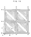
- FIG. 19 is a view showing a layout of a semiconductor wafer according to the eighth embodiment of the present invention.
- FIG. 20 is a view showing a layout of a semiconductor wafer according to the eighth embodiment of the present invention.
- FIG. 21 is a view showing a schematic structure of a comparative example to the relay chips according to the eighth embodiment of the present invention.
- FIG. 22 is a view showing a schematic structure of a relay chip according to the eighth embodiment of the present invention.
- FIG. 23 is a view showing a schematic structure of a semiconductor device according to the eighth embodiment of the present invention.
- FIG. 24 is a view showing a schematic structure of a semiconductor device according to the eighth embodiment of the present invention.
- FIG. 25 is a plan view of a wiring pattern of a wiring chip of a semiconductor device according to a ninth embodiment of the present invention.
- An MCP product includes a plurality of memory chips for different purposes and an ASIC such as a memory controller, which are stacked on an MCP substrate.
- ASIC such as a memory controller
- wire bonding For using wire bonding, it is common to use a wiring chip because wire bonding involves limitations such as the wire length or the like, and where a memory chip has a large size, it is difficult to connect an ASIC stacked on the memory chip directly to the MCP substrate by wiring.
- FIG. 12 is a cross-sectional view of an MCP including one ASIC 12 and one memory chip 11 .
- the memory chip 11 is provided on an MCP substrate, and the ASIC 12 as a memory controller and a wiring chip 13 are provided on the memory chip 11 .
- projection card connection electrode bumps 14 (hereinafter, referred to as the “bumps 14 ”) for directly connecting electrodes are provided.
- the memory chip is stacked on the MCP substrate 10 with an interlayer film 22 being interposed therebetween, and the ASIC 12 and the wiring chip 13 are stacked on the memory chip 11 with an interlayer film 22 being interposed therebetween.
- the memory chip 11 , the ASIC 12 and the wiring chip 13 are each electrically connected to the MCP substrate 10 by a bonding wire 21 .
- the ASIC and the wiring chip 13 are also electrically connected to each other by a bonding wire 21 .
- FIG. 13 is a plan view of an MCP including an ASIC, a plurality of memory chips and a plurality of wiring chips mounted on one substrate.
- FIG. 14 is a cross-sectional view of the MCP shown in FIG. 13 taken along line B-B′.
- two memory chips (upper memory chip and lower memory chip) 11 are mounted on the MCP substrate 10
- an ASIC 12 for a controller and two wiring chips 13 are mounted on the upper memory chip 11 .
- bumps 14 for directly connecting electrodes are provided on a bottom surface of the MCP substrate 10 .
- the lower memory chip is stacked on the MCP substrate 10 with an interlayer film 22 being interposed therebetween, and the ASIC 12 and the wiring chips 13 are stacked on the upper memory chip 11 with an interlayer film 22 being interposed therebetween. Between the two memory chips 11 , a spacer 11 is located with an interlayer film 22 being provided on and below the spacer 11 .
- each memory chip 11 and the MCP substrate 10 are electrically connected to each other by bonding wires 21 , each of which electrically connects a memory chip pad 17 of the memory chip 11 and an MCP pad 16 of the MCP substrate 10 .
- the ASIC 12 and the MCP substrate 10 are electrically connected to each other by bonding wires 21 , each of which electrically connects an ASIC pad 18 of the ASIC 12 and an MCP pad 16 .
- Each wiring chip 13 and the MCP substrate 10 are electrically connected to each other by bonding wires 21 , each of which electrically connects a wiring chip pad 19 of the wiring chip 13 and an MCP pad 16 .
- the ASIC 12 and each wiring chip 13 are electrically connected to each other by bonding wires 21 , each of which electrically connects an ASIC pad 18 and a wiring chip pad 19 .
- the MCP substrate 10 needs to be electrically connected with each memory chip 11 , the ASIC 12 and the like by a bonding wire 21 when these elements are mounted on the MCP substrate 10 .
- the wiring distance between the ASIC 12 and the MCP substrate 10 is very long, which makes connection difficult.
- the wiring distance between the ASIC pads 18 and the MCP pads 16 on the top side can be about the same as the wiring distance on the bottom side, and the wiring distance on the right side can be about the same as the wiring distance on the left side.
- the wiring distance on the right side and the left side is long.
- the wiring distance on the opposite side is much longer than in the case where the ASIC 12 is located at the center.
- the wiring chips 13 are provided.
- the wiring chips 13 are located adjacent to the ASIC 12 . Input/output lines of the ASIC 12 are connected between the ASIC pads 18 and the wiring chip pads 19 of the wiring chip 13 adjacent to the ASIC 12 . Where the wiring chips 13 have metal wires 20 in an L-shape, the wiring chip pads 19 , located in a direction perpendicular to the wiring chip pads 19 connected to the ASIC pads 18 , can be connected to the MCP pads 16 of the MCP substrate 10 . By providing the wiring chips 13 , it becomes easier to connect the ASIC pads 18 and the MCP pads 16 located in a direction perpendicular to the ASIC pads 18 .
- the metal wires 20 - 1 on an inner side and the metal wires 20 n on an outer side have approximately the same width, and each adjacent metal wires have approximately the same interval.
- Wiring pitches P 1 through Pn are also approximately the same.
- the wiring pitch P 1 is the sum of the width of the metal wire 20 - 1 and the interval between the metal wire 20 - 1 and the metal wire 20 - 2 adjacent to the metal wire 20 - 1 .
- the “inner side” refers to the side of a contact point of the two sides in the vicinity of the wiring chip pads 19 A 1 and 19 B 1 , among the plurality of metal wires provided on the wiring chip 13 , i.e., the side of the metal wire 20 - 1 .
- the “outer side” refers to the opposite side to the inner side, among the plurality of metal wires provided on the wiring chip 13 , i.e., the side of the metal wire 20 n .
- the width of one metal wire will be referred to as the “line width W”
- the width of the interval between one metal wire and a metal wire adjacent and outer to the one metal wire will be referred to as the “wiring space S”
- the sum of the width of one metal wire and the interval between one metal wire and a metal wire adjacent and outer to the one metal wire will be referred to as the “wiring pitch P”.
- the metal wire 20 - 1 on the inner side and the metal wire 20 n on the outer side are significantly difference in the wiring length as shown in FIG. 15 .
- the capacitance between the metal wire and the substrate and the wiring capacitance between the metal wire and the adjacent metal wire increase.
- the capacitance between the metal wire and the substrate and the wiring capacitance between the metal wire and the adjacent metal wire decrease.
- the line width W of the metal wire is wider, the capacitance per unit length between the metal line and the substrate increases.
- the metal wires are arranged at substantially the same line width W, substantially the same wiring space S and substantially the same wiring pitch P, and the metal wire 20 - 1 and the metal wire 20 are significantly different in the wiring length. Therefore, the wiring capacitance between the metal wire 20 - 1 and the metal wire adjacent thereto is significantly different from the wiring capacitance between the metal wire 20 n and the metal wire adjacent thereto.
- the above-mentioned wiring capacitance between adjacent metal wires appears as a capacitance of external pins of the MCP (in the example of FIG. 14 , the bumps 14 ). Therefore, when the MCP is used, the external pins each have a large capacitance and the capacitance is different among the external pins.
- Such an MCP in which the capacitances of the external pins are large and significantly different there among is used, prevents an increase in the signal processing speed and cannot easily reduce the power consumption.
- Such an MCP has a large skew (diversion in the timing of the signal input/output between the external pins), which reduces a margin of an operation speed or the like.
- the number of memory chips mounted on one MCP is increased in compliance with a demand for a larger memory capacity. Accordingly, the number of memory chips connected to one external pin is increased.
- the input/output pin capacitances of each chip are added together. Therefore, it is required to minimize the difference in the wiring capacitance between adjacent metal wires in the entire chip.
- FIG. 1 is a plan view showing a wiring pattern of a wiring chip of the semiconductor device according to the first embodiment of the present invention.
- FIG. 2 is a plan view of the semiconductor device according to the first embodiment of the present invention.
- FIG. 3 is a cross-sectional view of the semiconductor device shown in FIG. 2 taken along line A-A′.
- the length of each of the plurality of metal wires 20 for connecting wiring chip pads 19 on a wiring chip substrate 23 of a wiring chip 13 is made shorter than in the case where L-shaped metal wires are provided in the same size of wiring chip 13 .
- all the plurality of metal wires 20 in one chip do not have the same line width W.
- the line width W of each metal line is set to an arbitrary value (hereinafter, the line width set in this manner will be referred to as the “line width W adjustable at the time of designing” or “wiring width adjustable at the time of designing”).
- all the wiring spaces S in one chip are not the same.
- each wiring space is set to an arbitrary value (hereinafter, the wiring space set in this manner will be referred to as the “wiring space S adjustable at the time of designing” or “wiring interval adjustable at the time of designing”).
- the wiring space S adjustable at the time of designing or “wiring interval adjustable at the time of designing”.
- all the wiring pitches P in one chip are not the same. Instead, each wiring pitch is set to an arbitrary value (hereinafter, the wiring pitch set in this manner will be referred to as the “wiring pitch P adjustable at the time of designing”).
- the wiring width of each metal wire 20 , the wiring interval between each metal wire and a metal wire adjacent and outer thereto, and each wiring pitch as a sum of the wiring width and the wiring interval are set such that the difference in the wiring capacitance between each adjacent metal lines is minimum.
- wiring chip pads 19 A 1 through 19 An are provided inside one of four sides, and wiring chip pads 19 B 1 through 19 Bn are provided inside a side adjacent to the one side.
- the number of the wiring chip pads provided along the two adjacent sides is the same (n number of the wiring chip pads are provided).
- data which is input to the wiring chip pad 19 A 1 is output from the wiring chip pad 19 B 1 via the metal wire 20 - 1 .
- Data which is input to the wiring chip pad 19 B 1 is output from the wiring chip pad 19 A 1 via the metal wire 20 - 1 .
- data passes through the wiring chip 13 and therefore is output in a direction perpendicular to the direction in which the data is input.
- the metal wires 20 - 1 through 20 n for connecting the wiring chip pads 19 A 1 through 19 An and the wiring chip pad 19 B 1 through 19 Bn to each other have a trapezoidal shape with a base part removed (hereinafter, this shape will be referred to as the “trapezoid upper shape”) in order to shorten the metal wires 20 - 1 through 20 n .
- the metal wires can be straight.
- the wiring chip 13 according to the first embodiment the following structure is adopted in order to secure a certain wiring space S and also shorten the length of the metal wires.
- metal wires 20 have such a shape, sufficient wiring spaces S can be guaranteed by adjusting the lengths of the first part and the second part between adjacent metal wires 20 , and also the length of each metal wire 20 can be shortened as compared to the L-shaped metal wires 20 shown in FIG. 15 .
- FIG. 2 shows the semiconductor device according to the first embodiment.
- memory chips 11 are mounted on an MCP substrate 10
- two ASICs 12 and a wiring chip 13 are mounted on the top memory chip 11 .
- First wiring chip pads 16 provided in the MCP substrate 10 and connected to connection electrodes of the MCP hereinafter, the first wiring chip pads will be referred to as the “MCP pads”
- memory chip pads 17 provided on a substrate of each memory chip 11 are connected to each other by bonding wires 21 .
- second pads 18 provided on a substrate of each ASIC 12 hereinafter, the second pads 18 will be referred to as the “ASIC pads 18 ”
- the MCP pads 16 are connected to each other by bonding wires 21 .
- a part of the ASIC pads 18 of the ASIC 12 which is shown left in FIG. 2 and a part of the wiring chip pads 19 of the wiring chip 13 are connected to each other. With such connections, the ASIC pads 18 of the ASIC 12 shown left in FIG. 12 , which are not directly connected to the MCP pads 16 , are electrically connected to the MCP pads 16 via the wiring chip 13 .
- FIG. 3 is a cross-sectional view of the semiconductor device shown in FIG. 2 taken along line A-A′.
- the memory chips 11 are stacked on the MCP substrate 10 with interlayer films 22 and spacers 15 being interposed therebetween.
- the MCP substrate 10 may be formed of silicon, glass or the like. In the example of FIG. 3 , three memory chips 11 are stacked, but the number of memory chips 11 is not limited to three.
- On the top memory chip 11 two ASICs 12 and a wiring chip 13 are mounted.
- bumps 14 for directly connecting electrodes are provided on a bottom surface of the MCP substrate 10 .
- the MCP substrate 10 are connected to each other by the bonding wires 21 , and the ASIC pads (not shown in FIG. 3 ) of each of the two ASICs 12 and the MCP pads (not shown in FIG. 3 ) of the MCP substrate 10 are connected to each other by the bonding wires 21 .
- the ASIC 12 shown left in FIG. 3 and the wiring chip 13 are connected to each other by the bonding wires 21 .
- each bonding wire 21 can be shorter.
- only the ASIC 12 shown left is connected to the MCP pads 16 of the MCP substrate 10 by the wiring chip 13 .
- the ASIC pads of the ASIC 12 shown right and left can be connected to the MCP pads 16 .
- the bonding wires 21 for connecting each ASIC 12 and the wiring chip 13 can be shortened, and wires for connecting the wiring chip 13 and the MCP pads 16 can also be shortened.
- the metal wires 20 for connecting the wiring chip pads in the wiring chip are of the relatively short possible length owing to the trapezoid upper shape. Therefore, the total wiring length from the ASIC 12 to the MCP pads 16 of the MCP substrate 10 can also be shortened. As the number of memory chips 11 stacked on the MCP substrate 10 is increased, the number of wires increases, and the number of ASICs may be increased. This extends the length of bonging wires 21 for connecting the chips (including ASICs), which makes the wiring difficult.
- the semiconductor device according to the first embodiment of the present invention suppresses the length of the bonding wires 21 from being extended owing to the provision of the wiring chip 13 . This is also applicable even when the number of memory chips 11 stacked on the MCP substrate 10 is significantly increased or when the number of ASICs 12 mounted on the MCP is significantly increased.
- the metal wires 20 have the line width W adjustable at the time of designing.
- the innermost metal wire 20 - 1 which is relatively short and having a relatively small wiring capacitance with the adjacent metal wire 20 - 2 has a relatively wide line width W.
- the outermost metal wire 20 n which is relatively long and having a relatively large wiring capacitance with the adjacent metal wire 20 n ⁇ 1 has a relatively narrow line width W.
- the line width W of the metal wire 20 is set to be narrower as being closer to the outermost metal wire 20 n .
- the wiring capacitance between the relatively short adjacent metal wire 20 - 1 and the adjacent metal wire 20 - 2 can be increased whereas the wiring capacitance between the relatively long metal wire 20 n and the adjacent metal wire 20 n ⁇ 1 can be decreased.
- the metal wires 20 are arranged with a wiring space S adjustable at the time of designing. As shown in FIG. 1 , the wiring spaces S between the plurality of metal wires 20 - 1 through 20 n are not equal, but the wiring space S is set to be wider as being closer to the outermost wiring space Sn from the innermost wiring space S 1 .
- the wiring capacitance between the metal wire 20 - 1 and the adjacent metal wire 20 - 2 can be increased whereas the wiring capacitance between the metal wire 20 n and the adjacent metal wires 20 n ⁇ 1 can be decreased.
- the metal wires 20 are arranged with a wiring pitch P adjustable at the time of designing.
- the wiring pitches P each of which is the sum of the line width W of the metal wire 20 and the wiring space S between the metal wire 20 and the metal wire adjacent and outer thereto, are not equal.
- the wiring pitch P is set to be wider as being closer to the outermost pitch Pn from the innermost pitch P 1 .
- the wiring chip 13 of the semiconductor device includes the metal wires 20 - 1 through 20 n which have a trapezoid upper shape and are arranged with the line width W adjustable at the time of designing, the wiring space S adjustable at the time of designing and the wiring pitch P adjustable at the time of designing.
- the innermost and relatively short metal wire 20 - 1 is arranged with a relatively wide line width W 1 and a relatively narrow wiring space S 1 with the adjacent metal wire 20 - 2 . Therefore, the capacitance per unit length between the metal wire 20 - 1 and the wiring chip substrate 23 can be maximized, and the capacitance between the metal wire 20 - 1 and the adjacent metal wire 20 - 2 can also be maximized.
- the outermost and relatively long metal wire 20 n is arranged with a relatively narrow line width Wn and a relatively wide wiring space Sn with the adjacent metal wire 20 n ⁇ 1. Therefore, the capacitance per unit length between the metal wire 20 n and the wiring chip substrate 23 can be minimized, and the capacitance between the metal wire 20 n and the adjacent metal wire 20 n ⁇ 1 can also be minimized. As a result, the wiring capacitance regarding the innermost metal wire 20 - 1 is relatively increased, and the wiring capacitance regarding the outermost metal wire 20 n is relatively decreased. Therefore, the difference in the wiring capacitance between the plurality of metal wires 20 in the entire wiring chip 13 can be minimized.
- the metal wires 20 have a trapezoid upper shape and are arranged with the line width W adjustable at the time of designing, the wiring space S adjustable at the time of designing and the wiring pitch P adjustable at the time of designing.
- the wiring chip of the semiconductor device according to the first embodiment of the present invention may combine the line width W adjustable at the time of designing, the wiring space S adjustable at the time of designing and the wiring pitch P adjustable at the time of designing in any way.
- the line widths W 1 through Wn and the wiring spaces S 1 through Sn are adjustable at the time of designing whereas to set the wiring pitch P to be equal, i.e., to set all the wiring pitches to the wiring pitch P 1 .
- the line width W 1 of the innermost and relatively short metal wire 20 - 1 is set to be relatively wide, and the wiring space S 1 is set to be relatively narrow.
- the line width W is set to be narrower as being closer to the outermost line width Wn, whereas the wiring space S is set to be wider as being closer to the outermost wiring space Sn.
- the metal wires 20 with an equal line width W, an equal wiring space S, and an equal wiring pitch P. Namely, it is possible to set all the line widths W to the line width W 1 , to set all the wiring spaces S to the wiring space S 1 , and to set all the wiring pitches P to the wiring pitch P 1 , as in the conventional wiring chip.
- the line width W adjustable at the time of designing, the wiring space S adjustable at the time of designing and the wiring pitch P adjustable at the time of designing can be combined in any way with the wires having a trapezoid upper shape.
- the difference in the wiring capacitance between adjacent metal wires can be decreased in the entire wiring chip.
- the CR delay generated in each of a plurality of metal wires 20 located in a wiring chip can be minimized, and the difference in the CR delay among the plurality of metal wires 20 can be minimized. This can contribute to an increased signal transmission speed in the MCP. This will be described with reference to the drawings.
- FIG. 5 is a plan view showing a wiring pattern of a wiring chip 13 of a semiconductor device according to the second embodiment of the present invention.
- the wiring chip 13 of the semiconductor device according to the second embodiment of the present invention includes wiring chip pads 19 A 1 through 19 An provided inside one of four sides thereof, and wiring chip pads 19 B 1 through 19 Bn provided inside a side adjacent to the one side.
- the number of the wiring chip pads provided along the two adjacent sides is the same (n number of the wiring chip pads are provided).
- the wiring chip pads 19 A 1 through 19 An and the wiring chip pads 19 B 1 through 19 Bn are connected to each other by metal wires 20 - 1 through 20 n respectively, sequentially from the wiring chip pads closest to a contact point on the two sides.
- the wiring chip pads 19 are located such that the wiring space S is increased as being closer to the outermost wiring space Sn from the innermost wiring space S 1 , i.e., as being closer to the wiring chip pads 19 An and 19 Bn from the wiring chip pads 19 A 1 and 19 B 1 .
- the line width W of the metal wire 20 is set to be increased as being closer to the line width Wn from the innermost line width W 1 .
- the wiring pitch P is also set to be increased as being closer to the outermost wiring pitch Pn from the innermost wiring pitch P 1 .
- the outermost and relatively long metal wire 20 n is arranged with a relatively wide line width Wn and a relatively wide wiring space Sn with the adjacent metal wire 20 n ⁇ 1, and as a result, with a relatively wide wiring pitch Pn.
- the innermost and relatively short metal wire 20 - 1 is arranged with a relatively narrow line width W 1 and a relatively narrow wiring space S 1 with the adjacent metal wire 20 - 2 , and as a result, with a relatively narrow wiring pitch P 1 .
- the wiring capacitance between the outermost and relatively long metal wire 20 n and the adjacent metal wire 20 n ⁇ 1 is relatively decreased as compared to the wiring capacitance between the innermost and relatively short metal wire 20 - 1 and the adjacent metal wire 20 - 2 . Therefore, the wiring resistance of the metal wire 20 n can be decreased.
- the outermost metal wire 20 n is relatively long and therefore has a relatively large wiring capacitance with the adjacent metal wire 20 n ⁇ 1.
- the metal wire 20 n also has a relatively wide line width Wn, and therefore the capacitance per unit length between the metal wire 20 n and a wiring chip substrate 23 is also relatively large.
- the wiring resistance of the metal wire 20 n is relatively large.
- the wiring pitch Pn regarding the metal wire 20 n is wider than the wiring pitch P 1 regarding the metal wire 20 - 1 , the wiring capacitance between the metal wire 20 n and the adjacent metal wire 20 n ⁇ 1 is decreased, which also decreases the wiring resistance.
- the effects provided by the line width W, the wiring space Sn, and the wiring pitch Pn are mutually counteracted.
- the wiring resistance of the metal wire 20 n can be suppressed to be a certain appropriate level, and the CR delay can also be suppressed to be a certain appropriate level.
- the CR delay is determined based on the relationship of the length of each metal wire, the line width W and the wiring pitch P. Therefore, the CR delay can be adjusted by appropriately combining the line width W adjustable at the time of designing, the wiring space S adjustable at the time of designing and the wiring pitch P adjustable at the time of designing.
- the line width W and the wiring space S regarding the outermost metal wire 20 n are made wider than those regarding the innermost metal wire 20 - 1 , and hence the wiring capacitance between the metal wire 20 n and the adjacent metal wire 20 n ⁇ 1 and also the wiring resistance of the metal wire 20 n can be decreased.
- the largest CR delay generated in the metal wire 20 n can be effectively decreased, and also the difference between the CR delay generated in the metal wire 20 n and the CR delay generated in the adjacent metal wire 20 n ⁇ 1 can be effectively decreased. This can increase the signal transmission speed.
- the decreasing degree of the CR delay can be adjusted to a desired level by appropriately adjusting parameters such as, for example, the capacitance between each metal wire 20 and the wiring chip substrate 23 , the wiring capacitance between each adjacent metal wires 20 , and the specific resistance of each metal wire 20 .
- the line width W and the wiring space S are changeable, and the line width W or the wiring space S may be set to be equal depending on the number of metal wires located in the wiring chip 13 , the chip size of the wiring chip 13 , or the like.
- the length of the bonding wires 21 can be suppressed from being extended like in FIG. 2 . This is applicable even when the number of memory chips 11 stacked on the MCP substrate 10 is significantly increased or when the number of ASICs 12 mounted on the MCP is significantly increased.
- the size of the MCPs themselves is more and more decreased in response to the demand to reduce the mounting area.
- the number of wires can be increased while narrowing the wiring pitch P.
- FIG. 6 is a plan view of a wiring pattern of a wiring chip of a semiconductor device according to the third embodiment of the present invention.
- the wiring chip pads are located inside two adjacent side of four sides of the wiring chip with an equal number. Along each side, the wiring chip pads are located alternately in a plurality of lines, and arranged such that two or more pads are not aligned in a direction perpendicular to the respective side.
- a plurality of wiring chip pads 19 A and a plurality of wiring chip pads 19 B provided for connecting the wiring chip 13 to the ASIC and the MCP substrate are located along the two sides in a plurality of lines (two lines in this example) as described above.
- even numbered wiring chip pads 19 A 2 through 19 An ⁇ 1 are located in an inner line of the two lines, and odd numbered 19 A 1 through 19 An are located in an outer line.
- the odd numbered wiring chip pads 19 A 1 through 19 An, and the even numbered wiring chip pads 19 A 2 through 19 An ⁇ 1, are located alternately such that two or more wiring chip pads are not aligned in a direction perpendicular to the side.
- the wiring chip pads 19 A 1 , 19 A 2 through 19 An are arranged zigzag.
- the wiring chip pads 19 B 1 , 19 B 2 through 19 Bn are arranged in the same manner.
- the wiring chip pads 19 A 1 , 19 A 2 through 19 An are located in two lines
- the wiring chip pads 19 B 1 , 19 B 2 through 19 Bn are located in two lines.
- the number of lines is not limited to any specific number as long as there is no problem in the wiring of metal wires 20 - 1 through 20 n.
- the wiring chip pads 19 A 1 , 19 A 2 through 19 An and 19 B 1 , 19 B 2 through 19 Bn located in two lines are connected to each other by the L-shaped metal wires 20 - 1 through 20 n respectively, sequentially from the wiring chip pads closest to a contact point on the two sides.
- the metal wires 20 - 1 through 20 n are all arranged with an equal line width W 1 , an equal wiring space S 1 and an equal wiring pitch P 1 .
- the number of the wiring chip pads 19 mountable on the wiring chip 13 can be increased without enlarging the size of the wiring chip 13 .
- adjacent wiring chip pads 19 need to be located with a certain interval (the length of the longer side of the wiring chip pad 19 + ⁇ ) therebetween.
- the wiring chip pads 19 can be located with an interval with which the metal wires 20 are not overlapped and shortcircuiting, leak or the like is not caused between adjacent metal lines 20 .
- the wiring pitch P can be narrowed, which allows the number of wires to be increased in the same size of wiring chip.
- a part of the metal lines 20 can be shortened. This can suppress the wiring capacitance between adjacent metal lines.
- the metal lines 20 - 2 through 20 - n for connecting the wiring chip pads 19 A 2 through 19 An ⁇ 1 and 19 B 2 through 19 Bn ⁇ 1 located in the inner lines, even though being located outer to the metal lines 20 - 1 through 20 n for connecting the wiring chip pads 19 A 1 through 19 An and 19 B 1 through 19 Bn located in the outer lines, are not necessarily longer.
- the wiring chip pads 19 A 2 through 19 An ⁇ 1 and 19 B 2 through 19 Bn ⁇ 1 are located inner to the wiring chip pads 19 A 1 through 19 An and 19 B 1 through 19 Bn. Therefore, where the number of the metal wires 20 is the same, a part of the metal wires 20 can be shortened as compared to the metal wires 20 in the case where the wiring chip pads 19 are located in one line, as more specifically described below.
- the wiring chip pads 19 A 2 through 19 An ⁇ 1 and 19 B 2 through 19 Bn ⁇ 1 located in the inner line are provided inner to the wiring chip pads 19 A 1 through 19 An and 19 B 1 through 19 B, by the sum of the length of the shorter side of the inner wiring chip pads 19 A 2 through 19 An ⁇ 1 and 19 B 2 through 19 Bn ⁇ 1 and the interval between the inner wiring chip pads 19 A 2 through 19 An ⁇ 1 and 19 B 2 through 19 Bn ⁇ 1 and the outer wiring chip pads 19 A 1 through 19 An and 19 B 1 through 19 B. Therefore, the length of the metal wires 20 - 2 through 20 n ⁇ 1 can be shorter than the metal wires 20 - 1 through 20 n by the total of the above sums on the two sides. For this reason, the wiring capacitance, which is increased as the length of the metal wire 20 is increased, can be suppressed.
- the number of wires can be increased while narrowing the wiring pitch P owing to the wiring pattern of the wiring chip. This fulfills well the demand for a reduced size of semiconductor device itself.
- the length of the bonding wires 21 can be suppressed from being extended like in FIG. 2 . This is applicable even when the number of memory chips 11 stacked on the MCP substrate 10 is significantly increased or when the number of ASICs 12 mounted on the MCP is significantly increased.
- the number of wires can be increased while reducing the size of the wiring chip and also that the wiring capacitance between adjacent wires can be suppressed regarding a part of the wires.
- the wiring chip described above in the third embodiment with the trapezoid upper shape of the metal wires 20 , the line width W adjustable at the time of designing, the wiring space S adjustable at the time of designing and the wiring pitch P adjustable at the time of designing, the wiring capacitance between adjacent wires can be suppressed more effectively while allowing the number of wires to be increased.
- the wiring chip pads are located alternately in a plurality of lines such that two or more pads are not aligned in a direction perpendicular to the respective side, and the wiring chip pads are connected in the wiring chip by metal wires which have a trapezoid upper shape and are arranged with the line width W adjustable at the time of designing, the wiring space S adjustable at the time of designing and the wiring pitch P adjustable at the time of designing.
- FIG. 7 is a plan view of a wiring pattern of a wiring chip of a semiconductor device according to the fourth embodiment of the present invention.
- the wiring chip pads are located along two adjacent side of four sides of the wiring chip with an equal number. Along each side, the wiring chip pads are located alternately in a plurality of lines, and arranged such that two or more pads are not aligned in a direction perpendicular to the respective side.
- the metal wires for connecting the wiring chip pads have a trapezoid upper shape and are arranged with the line width W adjustable at the time of designing, the wiring space S adjustable at the time of designing and the wiring pitch P adjustable at the time of designing.
- a wiring chip substrate 23 of the wiring chip 13 on a wiring chip substrate 23 of the wiring chip 13 , a plurality of wiring chip pads 19 for connecting the wiring chip 13 to the external. ASIC and the MCP substrate are located along the two sides in two lines. As described above, the wiring chip pads 19 A 1 through 19 An and the wiring chip pads 19 A 2 through 19 An ⁇ 1 are located alternately in two lines such that two or more wiring chip pads are not aligned in a direction perpendicular to the side along which these wiring chips are located.
- the wiring chip pads 19 B 1 through 19 Bn and the wiring chip pads 19 B 2 through 19 Bn ⁇ 1 are located alternately in two lines such that two or more wiring chip pads are not aligned in a direction perpendicular to the side along which these wiring chips are located.
- the wiring chip pads are located in two lines along each side, but the number of lines is not limited to any specific number as long as there is no problem in the wiring of metal wires 20 - 1 through 20 n.
- a greater number of wiring chip pads 19 can be located than in the conventional art, and thus the number of wires can be increased.
- adjacent wiring chip pads 19 need to be located with a certain interval (the length of the longer side of the wiring chip pad 19 + ⁇ ) therebetween.
- the wiring chip pads 19 are located in a plurality of lines, even where the wiring chip pads 19 are partially overlapped in a direction perpendicular to the respective side, there is a sufficient interval between adjacent wiring chip pads 19 in each line.
- the wiring chip pads 19 can be located with an interval with which the metal wires 20 are not overlapped and short-circuiting, leak or the like is not caused between adjacent metal lines 20 .
- the interval between adjacent wiring chip pads 19 can be narrower than the length of the longer side of the wiring chip pads (in the case where the wiring chip pads are square, the length of each side thereof). As a result, a greater number of the wiring chip pads 19 can be located. This effect is the same as that of the third embodiment.
- the wiring chip pads 19 A 1 through 19 An and 19 A 2 through 19 n ⁇ 1 and wiring chip pads 19 B 1 through 19 Bn and 19 B 2 through 19 Bn ⁇ 1 are connected to each other respectively by the metal wires 20 - 1 through 20 n having a trapezoid upper shape, sequentially from the wiring chip pads closest to a contact point on the two sides.
- the input/output of the MCP can be input/output in a direction perpendicular to the input/output direction of the ASICs or the memory chips.
- the wiring chip pads are located alternately in two lines, such that two or more wiring chip pads are not aligned in a direction perpendicular to the respective side. Owing to this, a desired number of wires can be located in the wiring chip 13 even when the size of the wiring chip 13 is reduced.
- the interval between adjacent wiring chip pads 19 can be narrower than the length of the longer side of the wiring chip pads 19 (in the case where the wiring chip pads 19 are square, the length of each side thereof). This necessarily narrows the wiring space S between adjacent metal wires 20 . Therefore, the influence of the difference in the wiring capacitance between adjacent metal wires 20 is increased.
- the metal wires 20 in the wiring chip 13 have a trapezoid upper shape and are arranged with the line width W adjustable at the time of designing, the wiring space S adjustable at the time of designing and the wiring pitch P adjustable at the time of designing. Owing to such a structure, the difference in the wiring capacitance and the difference in the wiring resistance between adjacent metal wires 20 caused by the different lengths of the metal wires 20 can be decreased. As shown in FIG. 7 , the metal wires 20 - 1 through 20 n having a trapezoid upper shape can be shorter than the L-shaped metal wires. This effect provided by the wiring chip is the same as that in the first embodiment and the second embodiment.
- the line widths W 1 through Wn of the metal wires 20 - 1 through 20 n are set such that the line width W 1 of the innermost metal wire 20 - 1 is relatively wide, and the line width W is set to be decreased as being closer to the line width Wn of the outermost metal wire 20 n . Therefore, in the fourth embodiment, the capacitance between adjacent metal wires which is decreased as the metal wire is shorter, and the capacitance per unit length between the metal wire and the wiring chip substrate 23 which is increased as the line width W of the metal wire is wider, can be adjusted in accordance with the length of the metal wire.
- an inner and shorter metal wire 20 can be set to have a larger wiring capacitance with the adjacent metal wire and also to have a larger capacitance per unit length with the wiring chip substrate 23 .
- An outer and longer metal wire 20 can be set to have a smaller wiring capacitance with the adjacent metal wire and also to have a smaller capacitance per unit length with the wiring chip substrate 23 .
- the innermost metal wire 20 - 1 of the wiring chip 13 is set to have a relatively narrow wiring space S 1 .
- the wiring space S is set to be gradually increased as being closer to the outermost wiring space Sn.
- the wiring pitch P is decreased as being closer to the innermost wiring pitch P 1 and is increased as being closer to the outermost wiring pitch Pn.
- the innermost metal wire 20 - 1 Since the innermost metal wire 20 - 1 has a relatively wide line width W 1 and a relatively narrow wiring space S 1 , the capacitance per unit length between the metal wire 20 - 1 and the wiring chip substrate 23 is increased and the influence of the capacitance between the metal wire 20 - 1 and the adjacent metal wire 20 - 2 is also increased. However, the innermost metal wire 20 - 1 is relatively short and the capacitance between the metal wire 20 - 1 and the adjacent metal wire 20 - 2 is relatively small. As a result, the capacitance between these adjacent metal wires can be suppressed.
- the outermost metal wire 20 n is relatively long and thus the capacitance between the metal wire 20 n and the adjacent metal wire 20 n ⁇ 1 is relatively large.
- the outermost metal wire 20 n has a relatively narrow line width Wn and a relative narrow wiring space Sn. Therefore, the capacitance per unit length between the metal wire 20 n and the wiring chip substrate 23 is decreased, and thus the influence of the capacitance between the metal wire 20 n and the metal wire 20 n ⁇ 1 is relatively small. As a result, the capacitance between these adjacent metal wires can be suppressed.
- the wiring pattern of the wiring chip 13 of the semiconductor device according to the fourth embodiment of the present invention can effectively decrease the difference in the wiring capacitance and the difference in the wiring resistance between adjacent wires caused by the difference in the length of the wires.
- the number of wires can be increased, a semiconductor having a reduced mounting area can be provided.
- the length of the bonding wires 21 can be suppressed from being extended like in FIG. 2 . This is applicable even when the number of memory chips 11 stacked on the MCP substrate 10 is significantly increased or when the number of ASICs 12 mounted on the MCP is significantly increased.
- the wiring pattern of the wiring chip is applicable to wide wires such as a power supply wire or the like.
- FIG. 8 is a plan view of a wiring pattern of a wiring chip of a semiconductor device according to the fifth embodiment of the present invention. As shown in FIG. 8 , on a wiring chip substrate 23 of the wiring chip 13 , a plurality of wiring chip pads 19 A through 19 An and a plurality of wiring chip pads 19 B 1 through 19 Bn are respectively located inside two adjacent side of the four sides of the wiring chip 13 with an equal number (n number).
- the wiring chip pads 19 A 1 through 19 An and the wiring chip pads 19 B 1 through 19 Bn are connected to each other by metal wires 20 - 1 through 20 n respectively in the wiring chip 13 , sequentially from the wiring chip pads closest to a contact point on the two sides.
- the metal wires 20 - 1 through 20 n have a trapezoid upper shape in order to be shortened.
- the line widths W 1 through Wn of the metal wires 20 - 1 through 20 n of the trapezoid upper shape are not equal.
- the outermost metal wire 20 n which is relatively long and thus has the relatively large capacitance with the adjacent metal wire 20 n ⁇ 1 is set to have a relatively narrow line width Wn.
- the line width W is set to be gradually increased as being closer to the innermost metal wire 20 - 1 which is relatively short and has a relatively small capacitance with the adjacent metal wire 20 - 2 .
- the innermost wiring space S 1 is set to be narrowest, and the wiring space S is set to be gradually increased as being closer to the outermost wiring space Sn regarding the outermost metal wire 20 n which is relatively long and having a relatively large capacitance with the adjacent metal wire 20 n ⁇ 1.
- the power supply wire 24 is generally wider than the other metal wires 20 , and therefore the capacitance per unit between the power supply wire 24 and the wiring chip substrate 23 is larger. As a result, the difference in the wiring capacitance between adjacent wires in the wiring chip 13 is conspicuous. For this reason, the power supply wire 24 needs to be as short as possible and needs to be provided with a large wiring space S with the adjacent metal wire 20 .
- the wiring pattern of the wiring chip of the semiconductor device according to the fifth embodiment of the present invention can shorten the length of the power supply wire 24 owing to the trapezoid upper shape.
- the wiring space S is adjustable at the time of designing, a sufficiently wide wiring space S can be guaranteed even with the power supply wire 24 which is wider than the other metal wires 20 .
- the influence of the power supply wire 24 on the other metal wires 20 can be suppressed.
- the length of the bonding wires 21 can be suppressed from being extended like in FIG. 2 . This is applicable even when the number of memory chips 11 stacked on the MCP substrate 10 is significantly increased or when the number of ASICs 12 mounted on the MCP is significantly increased.
- the size of the MCPs themselves is more and more decreased in response to the demand to reduce the mounting area.
- the size of the MCPs is more decreased and accordingly the number of semiconductor memories or ASICs mounted on MCPs increases in the future, it is expected that a plurality of memory chips, and a plurality of ASICs for different uses, need to be provided. In such a case, the number of wires in the wiring chip is increased, and it may be necessary to extend the wires in two different directions from one wiring chip.
- the ASICs may be stacked on the memory chips.
- the number of wiring chips needs to be increased, which increases the cost of the MCP.
- the number of wires For example, in the case where an ASIC having ASIC pads along the periphery thereof is stacked on the memory chip with wiring, it is common to locate the ASIC in the vicinity of one of the four corners of the memory chip and to provide two wiring chips. Accordingly, in the case where two ASICs are used, four wiring chips are necessary. This increases the cost of the MCP. Occasionally, six chips including two ASICs and four wiring chips may not be provided due to the restricted mounting area of the MCP or the like. In order to solve these problems, it is required to increase the number of wires which can be provided on each wiring chip and also to arrange the wires such that signals are input/output in two different directions.
- FIG. 16 is a plan view of a wiring chip including L-shaped metal wires 20 located at an equal wiring pitch and arranged such that signals are input/output in two different directions.
- the metal wires 20 are arranged such that signals are input/output in two different directions in FIG. 16 , the apexes of the L-shaped metal wires 20 may contact each other in a central part of the wiring chip.
- the wiring chip pads 19 can only located in an area corresponding to a half or less of each side of the wiring chip. For this reason, the number of the metal wires 20 cannot be increased.
- the wiring chip 13 can provide connections in two different directions, i.e., between the left side and top side in FIG. 9 , and between the right side and bottom side in FIG. 9 .
- the wiring pattern of the wiring chip of the semiconductor device according to the sixth embodiment of the present invention can adjust the wiring pitch P, and therefore can provide a greater number of metal wires, as compared to the case shown in FIG. 16 where the L-shaped metal wires are arranged at an equal line width W, an equal wiring space S and an equal wiring pitch P.
- FIG. 10 is a plan view of a semiconductor device according to the sixth embodiment of the present invention.
- a memory chip 11 and two ASICs 12 a and 12 b are stacked on the MCP substrate 10 .
- the two ASICs 12 a and 12 b are located in the vicinity of the top right corner and the top left corner as shown in FIG. 10 among the four corners of the memory chip 11 .
- the length of the bonding wires 21 is limited.
- the wiring chip 13 shown in FIG. 9 adopting the wiring pattern of the semiconductor device according to the sixth embodiment of the present invention is located in a central part of the memory chip 11 .
- the wiring chip 13 is larger than the ASICs 12 a and 12 b in order to shorten the bonding wires 21 for connecting the wiring chip 13 with the ASICs 12 a or 12 b .
- the wiring chip pads 19 inside the four side of the wiring chip 13 are connected as described below with reference to FIG. 9 .
- the wiring chip pads 19 a 1 through 19 an along the top side in FIG. 9 and the wiring chip pads 19 d 1 through 19 dn along the left side in FIG. 9 are connected to each other by metal wires 20 A 1 through 20 An respectively.
- the wiring chip pads 19 c 1 through 19 cn along the bottom side in FIG. 9 and the wiring chip pads 19 b 1 through 19 bn along the right side in FIG. 9 are connected to each other by metal wires 20 B 1 through 20 Bn respectively.
- the wiring chip pads 19 of the wiring chip 13 and the ASIC pads 18 of the ASICs 12 a and 12 b are connected to each other by the bonding wires 21 .
- the wiring chip pads 19 of the wiring chip 13 , the ASIC pads 18 of the ASICs 12 a and 12 b , memory chip pads 17 of the memory chip 11 , and MCP pads 16 of the MCP substrate 10 are connected by the bonding wires 21 .
- the ASIC pads 18 along the right side of the ASIC 12 b on the top left corner of the memory chip 11 as shown in FIG. 10 are connected to the MCP pads 16 on a top part of the MCP substrate 10 as shown in FIG. 10 via the wiring chip 13 .
- the ASIC pads 18 along the left side of the ASIC 12 a on the top right corner of the memory chip 11 as shown in FIG. 10 are connected to the MCP pads 16 on a bottom part of the MCP substrate 10 as shown in FIG. 10 via the wiring chip 13 . Accordingly, one wiring chip 13 provides connections in two different directions, and thus the cost of the MCP can be reduced.
- the wiring pattern of the wiring chip of the semiconductor device according to the sixth embodiment of the present invention can provide connections in two different directions, while decreasing the difference in the wiring capacitance and the difference in the wiring resistance between adjacent metal wires of the wiring chip.
- the wiring pattern according to the sixth embodiment can also reduce the cost of the MCP.
- the length of the bonding wires 21 can be suppressed from being extended like in FIG. 2 . This is applicable even when the number of memory chips 11 stacked on the MCP substrate 10 is significantly increased or when the number of ASICs 12 mounted on the MCP is significantly increased.
- the length of the bonding wires 21 for connecting the left and right ASICs 12 a and 12 b with the MCP substrate 10 can be shortened. Therefore, even where the number of memory chips 11 and the ASICs 12 is increased with the integration being progressed, these elements can be connected by wire bonding with no need for any specific connection method. Thus, an increase of the cost of the MCP can be suppressed.
- the memory capacity can be increased in an MCP including a plurality of memory chips such as a microSD card or the like by arranging wires having a trapezoid upper shape with the line width W adjustable at the time of designing, the wiring space S adjustable at the time of designing and the wiring pitch P adjustable at the time of designing.
- a microSD card which is a super-compact SD card, has an outer dimension of 11.0 mm (W) ⁇ 15.0 mm (D) ⁇ 1.0 mm (H). As compared to the SD card, the microSD card is about half in thickness and 1/4.65 in surface area.
- the microSD card is not generally rectangular in shape, but has a cutaway portion at one of four corners of the rectangular shape and also has a generally C-shaped cutout portion for securing the microSD card when inserted into a slot of a cellular phone or the like. Accordingly, when mounting a memory chip on the micro SC card, it is necessary to stack the ASIC and the like in order to guarantee the maximum possible capacity of the memory chip. In order to connect the stacked chips, a wiring chip is necessary.
- a microSD card is smaller than the SD card with the surface area being 1/4.65. This requires the size of the ASIC and the wiring chip mounted thereon to be reduced. Since the microSD card has a unique shape, it is expected that the wiring chip to be mounted is also required have a unique shape in accordance with the shape of the microSD card, instead of a rectangular shape, as the capacity of the memory chip is increased.
- the semiconductor device according to the seventh embodiment of the present invention can fulfill the demand for an increased capacity of the microSD card.
- FIG. 11 is a plan view of a microSD card applying the semiconductor device according to the seventh embodiment of the present invention. With reference to FIG. 11 , the microSD card will be described.
- a microSD substrate 25 As shown in FIG. 11 , on a microSD substrate 25 , two capacitors 26 , a memory chip 11 , an ASIC 12 , and a wiring chip 13 are mounted.
- the memory chip 11 is provided with a maximum possible size as limited by the inner size of the microSD substrate 25 excluding the locations of the capacitors 26 .
- the size of the memory chip 11 is significantly different from the size of the ASIC 12 mounted thereon. Therefore, the wiring chip 13 is required for connecting the memory chip 11 and the ASIC 12 .
- the microSD substrate 25 needs to have an area for locating microSD pads 27 which are to be connected with the memory chip 11 and the like. In order to maximize the size of the memory chip 11 , it is considered to effectively use a top area of the microSD substrate 25 as shown in FIG. 11 having the generally C-shaped cutout portion as an area for locating the microSD pads 27 , instead of the left area as shown in FIG. 11 which is to be inserted into a cellular phone or the like.
- the number of connection wires is allowed to be increased while the difference in the wiring capacitance is decreased.
- This is realized by arranging, in the wiring chip, the metal wires having a trapezoid upper shape with the line width W adjustable at the time of designing, the wiring space S adjustable at the time of designing and the wiring pitch P adjustable at the time of designing. Therefore, even where the wiring chip 13 is formed to have a shape in conformity to the unique shape of the top area of the microSD substrate 25 as shown in FIG. 11 , a desired number of wires can be guaranteed.
- the wiring chip 13 a is not rectangular but is pentagonal as a result of one of the four corners of the rectangular shape being cut away in conformity to the shape of the microSD substrate 25 .
- the wires having a trapezoid upper shape according to one embodiment of the present invention, even the wiring chip 13 a with such a unique shape can be connected while a desired number of wires is guaranteed.
- the wiring chip pads 19 of the wiring chips 13 a and 13 b are arranged zigzag as described above in the third embodiment, the wiring chip pads 19 can be provided by a greater number even in the above-mentioned unique, small area than in the case where the wiring chip pads 19 are located in one line. Thus, it is easier to guarantee a required number of wires.
- the wiring capacitance and the wiring resistance may be different between adjacent wires.
- Such a difference in the wiring capacitance and the wiring resistance can be decreased by appropriately combining the line width W adjustable at the time of designing, the wiring space S adjustable at the time of designing and the wiring pitch P adjustable at the time of designing.
- a semiconductor device can provide direction conversion in a transverse direction of the bonding wires for connecting the chips in the MCP and can reduce the relaying cost of the bonding wires.
- FIG. 19 shows an exemplary layout of a wafer usable for producing the relay chips. Cut lines 31 through 36 surround quadrangles. A plurality of (seven in FIG. 19 ) bonding pads are provided along each side of each quadrangle. Metal wires each for connecting each bonding pad and a corresponding pad are provided. For example, bonding pads 37 and 38 which are each the p'th pad (p is an integer fulfilling 1 ⁇ p ⁇ 7) from an apex B are connected to each other by a metal wire 39 . The bonding pads and the metal wires are formed by proving a metal film on the wafer, then forming a resist mask on the metal film, etching the metal film by photolithography, and then removing the resist mask.
- FIG. 20 shows cut lines of the wafer usable for producing the triangular relay chips.
- the cut lines are represented with the reference numerals 31 through 36 and CUT 1 through CUT 3 .
- the cut lines CUT 1 through CUT 3 are along a diagonal line of the quadrangles defined by the cut lines 31 through 36 .
- the cut line CUT 1 is along a diagonal line of the quadrangle surrounded by the cut lines 31 , 32 , 35 and 36 (i.e., the straight line connecting apexes C and D).
- triangular relay chips By cutting the wafer along the cut lines 31 through 36 and CUT 1 through CUT 3 with a blade, triangular relay chips can be produced.
- a semiconductor material such as silicon or the like is usable.
- the material of the wafer may be the same as the material used for, for example, the circuit substrate on which the relay chips are to be mounted.
- a polyimide material or a glass epoxy material is usable.
- the material of the metal wires for example, aluminum, copper, nickel, or gold is usable.
- FIG. 21 shows a schematic view of another relay chip.
- a relay chip 51 has a quadrangular shape, and includes a plurality of (seven in FIG. 21 ) bonding pads 54 and 55 along each of a side 52 and a side 53 .
- Corresponding bonding pads 54 and 55 are connected to each other by wires 56 respectively.
- the wires 56 are formed of lines parallel to the sides 52 and 53 .
- the relay chips according to the eighth embodiment are obtained by cutting a quadrangular shape along a diagonal line. Therefore, the wafer gross is twice that in the above-described other embodiments.
- the semiconductor device can provide direction conversion in the transverse direction of the bonding wires and also provide the relay of the bonding at reduced cost.
- the relay chips shown in the eight embodiment are exemplary and the present invention is not limited to such structures.
- the wires for connecting the bonding pads of a triangular relay chip may include a non-straight wire.
- the number of the bonding pads along one of the two sides of the triangular relay chip may be different from the number of the bonding pads along the other side.
- the relay chips described above as examples in the eighth embodiment are triangular. This triangular shape is applicable to, for example, the wiring chip 13 described in the sixth embodiment.
- a wiring chip according to a ninth embodiment of the present invention can suppress the wiring capacitance between adjacent wires while increasing the number of the wires, and also can reduce the mounting area of the wiring chip more effectively. This is realized by arranging metal wires having a trapezoid upper shape with an appropriate combination of the line width W adjustable at the time of designing, the wiring space S adjustable at the time of designing and the wiring pitch P adjustable at the time of designing, and also shaping the entire relay chip to be triangular.
- the metal wires 20 B 1 through 20 Bn are set such that the relatively short metal wire 20 B 1 has a relatively wide line width Wn, and the relatively long metal wire 20 Bn has a relatively narrow line width W 1 .
- the wiring spaces S 1 through Sn are set to be increased as being closer to the outermost wiring space S 1 from the innermost wiring space Sn. Therefore, in each group of metal wires 20 , the difference in the wiring capacitance between adjacent metal wires 20 can be decreased.
- by shaping the wiring chip 13 to be triangular the mounting area of the wiring chip 13 can be reduced and thus the cost of the MCP can be more reduced.
- the wiring chip 13 described above as an example in the ninth embodiment is obtained by cutting the quadrangular wiring chip in the sixth embodiment along a diagonal line thereof.
- the triangular shape is not limited to being applied to the wiring chip 13 in the sixth embodiment, but is also applicable to the wiring chips 13 in FIG. 1 , FIG. 4 , FIG. 5 , FIG. 7 and FIG. 8 , with the line width W, the wiring pitch P or the like being adjusted.
- the number of chips stacked in the MCP is increased, the number of wires required for connecting the chips is increased.
- the wiring pitch P of the wiring chip 13 is increased to increase the number of metal wires in the wiring chip 13 while reducing the size of the wiring chip 13 as demanded.
- the variance in the length of the metal wires is increased between an inner area and an outer area of the wiring chip 13 . This may possibly increase the variance in the capacitance per unit length between the metal wire and the wiring chip substrate.
- the metal wires are formed on the wiring chip substrate with an insulating film being interposed therebetween. It is now found that the thickness of the insulating film influences the variance in the capacitance per unit length between the metal wire and the wiring chip substrate.
- the electrostatic capacitance C per unit area between the metal wire and the wiring chip substrate is derived from the following expression (1).
- ⁇ 0 is the dielectric constant of vacuum [F/m]
- ⁇ S is the relative dielectric constant of the insulating film between the metal wire and the wiring chip substrate
- S is the area of parallel plates facing each other between the metal wire and the wiring chip substrate
- t is the thickness of the insulating film [m].
- FIG. 26 shows the relationship between the thickness t of the insulating film and the electrostatic capacitance C per unit area.
- the vertical axis represents the electrostatic capacitance [fF/ ⁇ m 2 ] per unit area of parallel plates facing each other which are assumed to be the metal wire and the wiring chip substrate, and the horizontal axis represents the distance between the metal wire and the wiring chip substrate (i.e., the thickness t of the insulting film) [ ⁇ m].
- the electrostatic capacitance C is about 7 to about 0.3 [fF/ ⁇ m 2 ].
- the variance in the capacitance per unit length between the metal wire and the wiring chip substrate can be suppressed by adjusting the thickness t of the insulating film to be 0.1 [ ⁇ m] or greater.
- the graph in FIG. 26 shows the distance dependence characteristic of the electrostatic capacitance per unit area in the case where silicon is used as the material of the wiring chip substrate and SiO 2 is used as the material of the insulating film.
- the material of the wiring chip substrate is not limited to silicon and may be, for example, a polyimide material or a glass epoxy material.
- the material of the insulating film is not limited to SiO 2 and may be, for example, any insulating material suitable to a polyimide material, a glass epoxy material or other materials used for the wiring chip substrate.
- the adjustment of the thickness of the insulating film is also applicable to the first through eighth embodiments.
Abstract
Description
C=∈S/t=∈ 0·∈S ·S/t[F] (1),
Claims (11)
Applications Claiming Priority (4)
| Application Number | Priority Date | Filing Date | Title |
|---|---|---|---|
| JP2006-241656 | 2006-09-06 | ||
| JP2006241656A JP2008066456A (en) | 2006-09-06 | 2006-09-06 | Semiconductor device |
| JP2006282693A JP2008103406A (en) | 2006-10-17 | 2006-10-17 | Relay chip, manufacturing method thereof, and semiconductor device |
| JP2006-282693 | 2006-10-17 |
Publications (2)
| Publication Number | Publication Date |
|---|---|
| US20080054491A1 US20080054491A1 (en) | 2008-03-06 |
| US7732930B2 true US7732930B2 (en) | 2010-06-08 |
Family
ID=39150374
Family Applications (1)
| Application Number | Title | Priority Date | Filing Date |
|---|---|---|---|
| US11/851,118 Expired - Fee Related US7732930B2 (en) | 2006-09-06 | 2007-09-06 | Semiconductor device, relay chip, and method for producing relay chip |
Country Status (1)
| Country | Link |
|---|---|
| US (1) | US7732930B2 (en) |
Cited By (3)
| Publication number | Priority date | Publication date | Assignee | Title |
|---|---|---|---|---|
| US20090174043A1 (en) * | 2008-01-03 | 2009-07-09 | Linear Technology Corporation | Flexible contactless wire bonding structure and methodology for semiconductor device |
| US20130026656A1 (en) * | 2009-04-27 | 2013-01-31 | Kim Hye-Jin | Semiconductor packages and electronic systems including the same |
| US11410974B2 (en) | 2019-12-03 | 2022-08-09 | Kioxia Corporation | Semiconductor memory device |
Families Citing this family (9)
| Publication number | Priority date | Publication date | Assignee | Title |
|---|---|---|---|---|
| US6992503B2 (en) | 2002-07-08 | 2006-01-31 | Viciciv Technology | Programmable devices with convertibility to customizable devices |
| US7112994B2 (en) | 2002-07-08 | 2006-09-26 | Viciciv Technology | Three dimensional integrated circuits |
| US8643162B2 (en) | 2007-11-19 | 2014-02-04 | Raminda Udaya Madurawe | Pads and pin-outs in three dimensional integrated circuits |
| US7030651B2 (en) | 2003-12-04 | 2006-04-18 | Viciciv Technology | Programmable structured arrays |
| TWI419283B (en) * | 2010-02-10 | 2013-12-11 | Advanced Semiconductor Eng | Package structure |
| EP2866532A4 (en) * | 2012-09-07 | 2016-03-09 | Fujikura Ltd | Wiring board |
| US10971478B2 (en) | 2016-12-30 | 2021-04-06 | Intel Corporation | Interposer design in package structures for wire bonding applications |
| JP6928746B2 (en) * | 2017-04-10 | 2021-09-01 | ブリルニクス シンガポール プライベート リミテッド | Solid-state image sensor, manufacturing method of solid-state image sensor, and electronic equipment |
| CN113228265A (en) * | 2019-07-03 | 2021-08-06 | 富士电机株式会社 | Circuit structure of semiconductor assembly |
Citations (7)
| Publication number | Priority date | Publication date | Assignee | Title |
|---|---|---|---|---|
| US5329157A (en) * | 1992-07-17 | 1994-07-12 | Lsi Logic Corporation | Semiconductor packaging technique yielding increased inner lead count for a given die-receiving area |
| US5976911A (en) | 1997-12-08 | 1999-11-02 | Micron Technology, Inc. | Controlling impedances of an integrated circuit |
| JP2004056023A (en) | 2002-07-24 | 2004-02-19 | Oki Electric Ind Co Ltd | Semiconductor device and its manufacturing method |
| JP2004327993A (en) | 2003-04-26 | 2004-11-18 | Samsung Electronics Co Ltd | Multi-chip bga package |
| US6958532B1 (en) | 1999-06-18 | 2005-10-25 | Nec Electronics Corporation | Semiconductor storage device |
| US7009303B2 (en) | 2003-11-17 | 2006-03-07 | Renesas Technology Corp. | Multi-chip module |
| US7087844B2 (en) | 2003-12-16 | 2006-08-08 | Nitto Denko Corporation | Wiring circuit board |
-
2007
- 2007-09-06 US US11/851,118 patent/US7732930B2/en not_active Expired - Fee Related
Patent Citations (9)
| Publication number | Priority date | Publication date | Assignee | Title |
|---|---|---|---|---|
| US5329157A (en) * | 1992-07-17 | 1994-07-12 | Lsi Logic Corporation | Semiconductor packaging technique yielding increased inner lead count for a given die-receiving area |
| US5976911A (en) | 1997-12-08 | 1999-11-02 | Micron Technology, Inc. | Controlling impedances of an integrated circuit |
| US6958532B1 (en) | 1999-06-18 | 2005-10-25 | Nec Electronics Corporation | Semiconductor storage device |
| JP2004056023A (en) | 2002-07-24 | 2004-02-19 | Oki Electric Ind Co Ltd | Semiconductor device and its manufacturing method |
| US6836010B2 (en) | 2002-07-24 | 2004-12-28 | Oki Electric Industry Co., Ltd. | Semiconductor device include relay chip connecting semiconductor chip pads to external pads |
| JP2004327993A (en) | 2003-04-26 | 2004-11-18 | Samsung Electronics Co Ltd | Multi-chip bga package |
| US7064444B2 (en) | 2003-04-26 | 2006-06-20 | Samsung Electronics Co., Ltd. | Multi-chip ball grid array package |
| US7009303B2 (en) | 2003-11-17 | 2006-03-07 | Renesas Technology Corp. | Multi-chip module |
| US7087844B2 (en) | 2003-12-16 | 2006-08-08 | Nitto Denko Corporation | Wiring circuit board |
Cited By (10)
| Publication number | Priority date | Publication date | Assignee | Title |
|---|---|---|---|---|
| US20090174043A1 (en) * | 2008-01-03 | 2009-07-09 | Linear Technology Corporation | Flexible contactless wire bonding structure and methodology for semiconductor device |
| US20110042792A1 (en) * | 2008-01-03 | 2011-02-24 | Linear Technology Corporation | Flexible contactless wire bonding structure and methodology for semiconductor device |
| US7960845B2 (en) * | 2008-01-03 | 2011-06-14 | Linear Technology Corporation | Flexible contactless wire bonding structure and methodology for semiconductor device |
| US8269355B2 (en) | 2008-01-03 | 2012-09-18 | Linear Technology Corporation | Flexible contactless wire bonding structure and methodology for semiconductor device |
| US20130026656A1 (en) * | 2009-04-27 | 2013-01-31 | Kim Hye-Jin | Semiconductor packages and electronic systems including the same |
| US8643193B2 (en) * | 2009-04-27 | 2014-02-04 | Samsung Electronics Co., Ltd. | Semiconductor packages and electronic systems including the same |
| US8901749B2 (en) | 2009-04-27 | 2014-12-02 | Samsung Electronics Co., Ltd. | Semiconductor packages and electronic systems including the same |
| US9184156B2 (en) | 2009-04-27 | 2015-11-10 | Samsung Electronics Co., Ltd. | Semiconductor packages and electronic systems including the same |
| US11410974B2 (en) | 2019-12-03 | 2022-08-09 | Kioxia Corporation | Semiconductor memory device |
| US11876080B2 (en) | 2019-12-03 | 2024-01-16 | Kioxia Corporation | Semiconductor memory device |
Also Published As
| Publication number | Publication date |
|---|---|
| US20080054491A1 (en) | 2008-03-06 |
Similar Documents
| Publication | Publication Date | Title |
|---|---|---|
| US7732930B2 (en) | Semiconductor device, relay chip, and method for producing relay chip | |
| US6172418B1 (en) | Semiconductor device and method for fabricating the same | |
| US8338963B2 (en) | Multiple die face-down stacking for two or more die | |
| US7064444B2 (en) | Multi-chip ball grid array package | |
| US9437579B2 (en) | Multiple die face-down stacking for two or more die | |
| US9418964B2 (en) | Chip package structure | |
| JP4580671B2 (en) | Semiconductor device | |
| US20060148130A1 (en) | Memory chip and semiconductor device using the memory chip and manufacturing method of those | |
| JP3221486B2 (en) | Semiconductor package | |
| US7642632B2 (en) | Pad redistribution chip for compactness, method of manufacturing the same, and stacked package using the same | |
| US11569200B2 (en) | Semiconductor package and method of manufacturing semiconductor package | |
| US11158621B2 (en) | Double side mounted large MCM package with memory channel length reduction | |
| CN107958889A (en) | Semiconductor device | |
| JP2011222807A (en) | Semiconductor device | |
| US11830849B2 (en) | Semiconductor device with unbalanced die stackup | |
| JPH1140745A (en) | Semiconductor device and electronic device incorporating the same | |
| US9318470B2 (en) | Semiconductor device | |
| WO2024060318A1 (en) | Semiconductor structure and manufacturing method therefor | |
| US20110095414A1 (en) | Semiconductor substrate, laminated chip package, semiconductor plate and method of manufacturing the same | |
| US20230110997A1 (en) | Semiconductor device | |
| US20230096170A1 (en) | Semiconductor package | |
| CN216213447U (en) | Power module package | |
| JP2008066456A (en) | Semiconductor device | |
| KR20230143497A (en) | Semiconductor package and method for manufacturing the same | |
| JPH05206375A (en) | Multi-chip module |
Legal Events
| Date | Code | Title | Description |
|---|---|---|---|
| AS | Assignment |
Owner name: KABUSHIKI KAISHA TOSHIBA, JAPAN Free format text: ASSIGNMENT OF ASSIGNORS INTEREST;ASSIGNORS:MAKINO, EIICHI;OHSHIMA, SHIGEO;OKUMURA, NAOHISA;REEL/FRAME:019981/0128 Effective date: 20070926 Owner name: KABUSHIKI KAISHA TOSHIBA,JAPAN Free format text: ASSIGNMENT OF ASSIGNORS INTEREST;ASSIGNORS:MAKINO, EIICHI;OHSHIMA, SHIGEO;OKUMURA, NAOHISA;REEL/FRAME:019981/0128 Effective date: 20070926 |
|
| FEPP | Fee payment procedure |
Free format text: PAYOR NUMBER ASSIGNED (ORIGINAL EVENT CODE: ASPN); ENTITY STATUS OF PATENT OWNER: LARGE ENTITY |
|
| FPAY | Fee payment |
Year of fee payment: 4 |
|
| FEPP | Fee payment procedure |
Free format text: MAINTENANCE FEE REMINDER MAILED (ORIGINAL EVENT CODE: REM.) |
|
| LAPS | Lapse for failure to pay maintenance fees |
Free format text: PATENT EXPIRED FOR FAILURE TO PAY MAINTENANCE FEES (ORIGINAL EVENT CODE: EXP.) |
|
| STCH | Information on status: patent discontinuation |
Free format text: PATENT EXPIRED DUE TO NONPAYMENT OF MAINTENANCE FEES UNDER 37 CFR 1.362 |
|
| FP | Lapsed due to failure to pay maintenance fee |
Effective date: 20180608 |