EP2232589B1 - Quantentunnelungs-fotodetektorarray - Google Patents
Quantentunnelungs-fotodetektorarray Download PDFInfo
- Publication number
- EP2232589B1 EP2232589B1 EP07852299.2A EP07852299A EP2232589B1 EP 2232589 B1 EP2232589 B1 EP 2232589B1 EP 07852299 A EP07852299 A EP 07852299A EP 2232589 B1 EP2232589 B1 EP 2232589B1
- Authority
- EP
- European Patent Office
- Prior art keywords
- opposing
- electrodes
- photodetector array
- array
- quantum tunneling
- Prior art date
- Legal status (The legal status is an assumption and is not a legal conclusion. Google has not performed a legal analysis and makes no representation as to the accuracy of the status listed.)
- Active
Links
Images


Classifications
-
- H—ELECTRICITY
- H10—SEMICONDUCTOR DEVICES; ELECTRIC SOLID-STATE DEVICES NOT OTHERWISE PROVIDED FOR
- H10F—INORGANIC SEMICONDUCTOR DEVICES SENSITIVE TO INFRARED RADIATION, LIGHT, ELECTROMAGNETIC RADIATION OF SHORTER WAVELENGTH OR CORPUSCULAR RADIATION
- H10F39/00—Integrated devices, or assemblies of multiple devices, comprising at least one element covered by group H10F30/00, e.g. radiation detectors comprising photodiode arrays
- H10F39/10—Integrated devices
- H10F39/12—Image sensors
-
- H—ELECTRICITY
- H10—SEMICONDUCTOR DEVICES; ELECTRIC SOLID-STATE DEVICES NOT OTHERWISE PROVIDED FOR
- H10F—INORGANIC SEMICONDUCTOR DEVICES SENSITIVE TO INFRARED RADIATION, LIGHT, ELECTROMAGNETIC RADIATION OF SHORTER WAVELENGTH OR CORPUSCULAR RADIATION
- H10F39/00—Integrated devices, or assemblies of multiple devices, comprising at least one element covered by group H10F30/00, e.g. radiation detectors comprising photodiode arrays
- H10F39/10—Integrated devices
- H10F39/107—Integrated devices having multiple elements covered by H10F30/00 in a repetitive configuration, e.g. radiation detectors comprising photodiode arrays
-
- H—ELECTRICITY
- H10—SEMICONDUCTOR DEVICES; ELECTRIC SOLID-STATE DEVICES NOT OTHERWISE PROVIDED FOR
- H10K—ORGANIC ELECTRIC SOLID-STATE DEVICES
- H10K39/00—Integrated devices, or assemblies of multiple devices, comprising at least one organic radiation-sensitive element covered by group H10K30/00
- H10K39/30—Devices controlled by radiation
- H10K39/32—Organic image sensors
Definitions
- the present invention relates broadly to quantum tunneling photodetector array and to a method of generating an image.
- CCD charge coupled device
- CMOS complimentary metal-oxide-semiconductor
- example embodiments of the present invention seek to provide an alternative image sensor and a method of generating an image in view of the ongoing and increasing demand for image sensors.
- a quantum tunneling photodetector array comprising an array of pairs of opposing first and second electrodes; a photo-sensitive insulating material disposed between the opposing first and second electrodes of the respective pairs; and an electrical circuit for detecting photo-assisted quantum tunneling currents between the opposing first and second electrode of the respective pairs.
- the claimed quantum tunneling photodetector is characterized in that the array of opposing first and second electrodes comprises a cross-grid of a first set of electrode nano wires and a second set of electrode nano wires, such that the first and second electrodes are constituted as opposing sections of the electrode nano wires of the first and second sets at projected cross-points of the cross-grid.
- a separation distance between the first and second electrodes may be substantially fixed.
- the opposing first and second electrodes may be supported on a first substrate and a second substrate respectively.
- the insulating material may be disposed between the first and second substrates.
- the insulating material may comprise a soft matter material.
- the soft matter material may comprise one or more of a group consisting of thiols, self assembled monolayers (SAMs), organic solvents, perfluoropolyether PFPE, organic solvents, and polymeric brushes.
- the insulating material may comprise a solid state material.
- the solid state material may comprise one or more of a group consisting of a dielectric material, or a doped heterostructure double well barrier such as Al x Ga 1-x As/GaAs/Al x Ga 1-x As.
- At least one of the first and second substrates may be transparent.
- the photodetector array may further comprise spacer elements maintaining the substantially fixed separation distance and between the first and second electrodes.
- the spacer elements may further maintain a parallelism of the pairs of first and second electrodes.
- the spacer elements may be formed as separate solid state material spacers or are incorporated into the photo-sensitive material.
- the first and second sets of electrode wires may be disposed at about 90° with respect to each other.
- the electrical circuit may comprise individual electrical connections to the electrode wires of the first and second sets.
- the electrical circuit may further comprise a multiplexer component for demultiplexing electrical signals from the first and second sets of electrode wires for detecting the quantum tunneling currents between the opposing sections of the electrode wires of the first and second sets.
- the array of opposing first and second electrodes may be constituted as first and second sets of pixel electrodes respectively.
- the electrical circuit may comprise individual electrical connections to the pixel electrodes of the first and second sets.
- the electrical circuit may further comprise a source for applying a potential difference across the first and second opposing electrodes.
- a method of generating an image comprising using a quantum tunneling photodetector array as defined in the first aspect.
- a method of generating an image comprising the steps of detecting photo-assisted quantum tunneling currents between opposing first and second electrodes of respective ones of an array of pairs of the opposing first and second electrodes; and generating the
- Figure 1 shows a plane view of a quantum tunneling photodetector array 100 according to an example embodiment.
- the array 100 comprises a first set 102 of electrode wires here in the form of nano wires e.g. 104.
- a second set 106 of electrode wires in the form of nano wires e.g. 108 is disposed at about 90° with respect to the first set 102, thus forming a cross-grid of nano wires.
- the nano wires e.g. 104, 108 of the first and second sets 102, 106 respectively are disposed with a fixed separation distance therebetween, i.e. the sets 102 and 106 are at a fixed separation distance along an axis perpendicular to the plane of the drawing in Figure 1 .
- Electric circuit components 110, 112 are provided, and are electrically interconnected into individual ones of the nano wires e.g. 108, 104 of the second and first set 106, 102 respectively.
- the electrical circuit components 110, 112 are controlled to apply a potential difference between the nano wires e.g. 104, 108 of the first and second sets 102, 106, to read tunneling currents flowing between projected cross-over points of the grid, and to determine which projected cross-over point was struck by light as described below.
- the cross-grid of the first and second sets 102, 106 of nano wires constitutes an array of opposing first and second electrodes in the formed of opposing sections e.g. 200 of the nano wire e.g. 202 and a corresponding opposing section (hidden in Figure 2 ) of the nano wire 204 at projected cross-points of the cross-grid.
- the electrical circuit components 110, 112 are additionally configured to function as a muttiplexer for de-multiplexing electrical signals from the nano wires e.g. 202, 204 of the first and second sets 102, 106 for detecting photo-assisted quantum tunneling currents between the opposing sections of the nano wires e.g. 202, 204 at the projected cross-points of the cross-grid, are understood in the art, and will not be described herein in more detail.
- Out of many possible multiplexer components and techniques for interrogating a network of sensing lines in a cross-grid arrangement reference is made to for example P.J. Kuekes, R.S. Williams, Demultiplexer for a molecular wire crossbar network (MWCN DEMUX) United States Patent 6,256,767 for description of an example multiplexer components and techniques suitable for use in example embodiments of the present invention.
- Figure 3 shows a cross-sectional view of the quantum tunneling photodetector array 100 of the example embodiment.
- the first set 102 of nano wires e.g. 300 is embedded in a transparent substrate 302.
- the second set 106 of nano wires e.g. 304 is also embedded in a transparent substrate 306.
- only one of the sets 102, 106 of nano wires may be embedded in a transparent material, while the other set can be embedded in an opaque material substrate.
- the transparent substrates 302. 306 can comprise glass substrates, but it will be appreciated that different transparent materials can be used in different embodiments, including, but not limited to quartz, sapphire transparent oxides (TOX), semiconductor materials such as silicon or insulating or semiconducting oxides. The choice of material can also depend on the relevant wavelength of interest
- example embodiment is not limited to operation in the visible wavelength range, but can be adapted to different wavelength ranges, including an infrared (IR) wavelength range or ultra-violet.
- IR infrared
- An insulating material 308 is disposed between the substrate 302, 306, in the fixed separation distance gap between the first and second sets 102, 106 of nano wires.
- the insulating material 308 is chosen to have photo-sensitive properties, more particular the material 308 is chosen such that photo-assisted quantum tunneling can be achieved between the nano wires of the first and second sets 102, 106 at opposing sections of the nano wires e.g. 300, 304 at projected cross-points e.g. 310 of the cross-grid.
- Figure 4 shows a detail of Figure 3 .
- photons 400 entering the photo-sensitive material 308 interact with the photo-sensitive material 308 to achieve photo-assisted quantum tunneling 401 between opposing sections 402, 404 of nano wires 300, 304 of the first and second sets of nano wires respectively.
- the electrical circuit components e.g. 110 are configured for applying a potential difference across the nano wires e.g. 300, 304 of the first and second sets of nano wires, and for de-multiplexing electrical signals from the nano wires e.g. 300, 304 of the first and second sets for detecting the quantum tunneling currents between the opposing sections 402, 404 of the nano wires 300, 304.
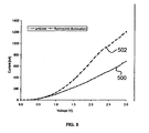
- Figure 5 shows an example plot of quantum tunneling current as a function of potential difference, illustrating a comparison between measurements in an ambient illumination (curve 500) and with fluorescent light illumination (502).
- curve 500 an ambient illumination
- fluorescent light illumination 502
- the effect of photo-assisted quantum tunneling is evidenced by the increase in measured tunneling current at a given applied potential difference.
- Example embodiments of the present invention exploit the photo-assisted quantum tunneling effect to sense photons or optical signals at the various projected cross-points of the cross-grid of nano wires for implementation of image sensors.
- threshold based signal processing or analog (spectral) signal processing can be performed in example embodiments, to generate an image detected by the quantum tunneling photodetector array.
- Threshold based signal processing and analog (spectral) signal processing are understood in the art, and will not be described herein in more detailed.
- the photo-sensitive material 308 in the example embodiment can comprise thiol.
- the photo-sensitive material 308 may be a soft matter material, or a solid state material in different embodiments.
- suitable photo-sensitive materials include, but are not limited to, thiols, self assembled monolayers (SAMs), organic solvents, perfluoropolyether (PFPE), or solid state materials such as a doped heterostructure double well barrier such as Al x Ga 1-x As/GaAs/Al x Ga 1-x As or dielectric materials as used in Resonant Tunneling Diodes (RTD), see for example H.Mizuta and T. Tanoue, The Physics and Applications of Resonant Tunneling Diodes, Cambridge U.P., 1995 .
- the deposition of such photo-sensitive materials is understood in the art, and will not be described herein in more detail.
- the fixed separation distance and two-dimensional parallelism between substrates 302 and 306 with embedded nanowire arrays 102 and 106 is chosen such that tunneling current can flow between the projected nanowire cross-over points e.g 310.
- the photo-sensitive material 308 is a soft matter material
- separate solid state spacers e.g. 311 can be used to keep the separation distance fixed and the substrates 302, 306 parallel.
- Solid state, e.g. oxide, spacers 311 can be fabricated on one or both substrates 302, 306, outside the nanowire arrays 102, 106 areas.
- molecular species that can provide structural stiffness may be incorporated into the soft matter material.
- carbon bucky-balls C 60 or other suitable species can be provided in solution in the soft matter material.
- the separation distance can be kept fixed and the substrates 302, 306 can be kept parallel through the structural integrity of the solid state material itself, and/or through use of separate spacers e.g. 311 between the substrates 302 and 306.
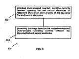
- Figure 6 shows a flow chart 600 illustrating a method of generating an image according to an example embodiment.
- photo-assisted quantum tunnelling currents between opposing first and second electrodes of respective ones of an array of pairs of the opposing first and second electrodes are detected.
- the image is generated based on the respective detected photo-assisted tunnelling currents between the opposing first and second electrodes.
- the example embodiments described have applications as image sensors in various optical devices, including, but not limited to, camera cell phones, camera PA devices, digital still cameras, digital video cameras, embedded cameras in PCs, automotive rear view cameras or night vision cameras.
- the example embodiments can provide image sensors with operating voltages suitable for hand-held, battery operated devices, for example in the range from about 0 to 25 volts, and with low power consumption, for example in the milli Watt range.
- the sets of electrode wires in the cross-grid may be disposed at different, non-zero angles with respect to each other, other than the about 90° described for the example embodiment.
- the present invention is not limited to implementation with sets of electrode wires. Rather, in different embodiments the array of pairs of opposing first and second electrode elements can be implemented using two opposing sets of pixel electrode arrays.
- the electrical circuit for detecting the photo-assisted quantum tunneling current between the opposing first and second pixel electrodes comprises individual electrical connections to the pixel electrodes, for pixel-ised image sensing similar to CCD or CMOS based image sensors.
Landscapes
- Light Receiving Elements (AREA)
- Solid State Image Pick-Up Elements (AREA)
- Photometry And Measurement Of Optical Pulse Characteristics (AREA)
Claims (11)
- Tunneleffekt-Photodetektoranordnung umfassend:eine Anordnung (100) von Paaren von entgegengesetzten ersten (102,104) und zweiten (106,108) Elektroden;ein photosensitives Isolationsmaterial (308), das zwischen den entgegengesetzten ersten (102, 104) und zweiten (106, 108) Elektroden der jeweiligen Paare angeordnet ist; undeinen elektrischen Stromkreis (110, 112) zur Detektion von photounterstützten Tunneleffekt-Strömen zwischen den entgegengesetzten ersten (102, 104) und zweiten (106, 108) Elektroden der jeweiligen Paare,dadurch gekennzeichnet, dass
die Anordnung (100) der entgegengesetzten ersten (102, 104) und zweiten (106, 108) Elektroden ein Raster aus einer ersten Einheit (102) von Elektrodennanodrähten und aus einer zweiten Einheit (106) von Elektrodennanodrähten umfasst, so dass die ersten (102, 104) und zweiten (106, 108) Elektroden als entgegengesetzte Abschnitte (200) der Elektrodennanodrähte (202, 204) der ersten (102) und zweiten (106) Einheiten an projizierten Kreuzungspunkten des Gitters ausgebildet sind. - Photodetektoranordnung nach Anspruch 1, dadurch gekennzeichnet, dass die entgegengesetzten ersten (102,104) und zweiten (106,108) Elektroden von einem ersten (302) beziehungsweise einem zweiten Substrat (306) getragen werden.
- Photodetektoranordnung nach Anspruch 2, dadurch gekennzeichnet, dass das Isolationsmaterial (308) zwischen dem ersten Substrat (302) und dem zweiten Substrat (306) angeordnet ist.
- Photodetektoranordnung nach Anspruch 3, dadurch gekennzeichnet, dass das Isolationsmaterial (308) ein oder mehr Elemente einer Gruppe umfasst, die Thiole, selbstorganisierende Monoschichten (SAMs), organische Lösungsmittel, Perfluoropolyether PFPE, organische Lösungsmittel und Polymerbürsten umfasst.
- Photodetektoranordnung nach Anspruch 1, dadurch gekennzeichnet, dass die erste Einheit (102) und zweite Einheit (106) von Elektrodennanodrähten (104, 202; 108, 204) ungefähr in einem Winkel von 90° zueinander angeordnet sind.
- Photodetektoranordnung nach Anspruch 1 oder 5, dadurch gekennzeichnet, dass der elektrische Schaltkreis (110, 112) individuelle elektrische Kontakte zu den Elektrodennanodrähten (104, 202; 108, 204) der ersten Einheit (102) und zweiten Einheit (106) umfasst.
- Photodetektoranordnung nach Anspruch 6, dadurch gekennzeichnet, dass der elektrische Schaltkreis (110, 112) des Weiteren eine Multiplex-Komponente umfasst, um elektrische Signale der ersten Einheit (102) und der zweiten Einheit (106) von Elektrodennanodrähten (104, 202; 108, 204) zu demultiplexen, um Tunneleffekt-Ströme zwischen den entgegengesetzten Abschnitten (200) der Elektrodennanodrähte (104, 202; 108, 204) der ersten Einheit (102) und zweiten Einheit (106) zu detektieren.
- Photodetektoranordnung nach einem beliebigen der Ansprüche 1 bis 4, dadurch gekennzeichnet, dass die Anordnung von entgegengesetzten ersten (102, 104) und zweiten (106, 108) Elektroden als erste beziehungsweise zweite Einheiten von Pixelelektroden ausgebildet ist.
- Photodetektoranordnung nach einem beliebigen der vorherigen Ansprüche, dadurch gekennzeichnet, dass der elektrische Schaltkreis (110, 112) ferner eine Quelle umfasst, um eine Potenzialdifferenz zwischen den ersten und zweiten entgegengesetzten Elektroden anzulegen.
- Verfahren zur Erzeugung eines Bildes, wobei eine Tunneleffekt-Photodetektoranordnung (100) nach einem beliebigen der vorherigen Ansprüche verwendet wird.
- Verfahren zur Erzeugung eines Bildes umfassend folgende Schritte: Detektion von photounterstützten Tunneleffekt-Strömen zwischen entgegengesetzten entsprechenden ersten (102, 104) und zweiten (106, 108) Elektroden einer Anordnung (100) von Paaren von entgegengesetzten ersten (102, 104) und zweiten (106, 108) Elektroden, wobei eine Tunneleffekt-Photodetektoranordnung (100) nach einem beliebigen der Ansprüche 1 bis 10 verwendet wird; und das Bild auf Grundlage der jeweils detektierten photounterstützten Tunneleffekt-Ströme zwischen den entgegengesetzten ersten (102, 104) und zweiten (106, 108) Elektroden erzeugt wird.
Priority Applications (1)
| Application Number | Priority Date | Filing Date | Title |
|---|---|---|---|
| EP13184689.1A EP2680321B1 (de) | 2007-12-18 | 2007-12-18 | Quantum-Tunneleffekt-Photodetektoranordnung |
Applications Claiming Priority (1)
| Application Number | Priority Date | Filing Date | Title |
|---|---|---|---|
| PCT/SG2007/000433 WO2009078809A1 (en) | 2007-12-18 | 2007-12-18 | Quantum tunneling photodetector array |
Related Child Applications (1)
| Application Number | Title | Priority Date | Filing Date |
|---|---|---|---|
| EP13184689.1A Division EP2680321B1 (de) | 2007-12-18 | 2007-12-18 | Quantum-Tunneleffekt-Photodetektoranordnung |
Publications (3)
| Publication Number | Publication Date |
|---|---|
| EP2232589A1 EP2232589A1 (de) | 2010-09-29 |
| EP2232589A4 EP2232589A4 (de) | 2011-02-16 |
| EP2232589B1 true EP2232589B1 (de) | 2013-11-20 |
Family
ID=40795773
Family Applications (2)
| Application Number | Title | Priority Date | Filing Date |
|---|---|---|---|
| EP07852299.2A Active EP2232589B1 (de) | 2007-12-18 | 2007-12-18 | Quantentunnelungs-fotodetektorarray |
| EP13184689.1A Active EP2680321B1 (de) | 2007-12-18 | 2007-12-18 | Quantum-Tunneleffekt-Photodetektoranordnung |
Family Applications After (1)
| Application Number | Title | Priority Date | Filing Date |
|---|---|---|---|
| EP13184689.1A Active EP2680321B1 (de) | 2007-12-18 | 2007-12-18 | Quantum-Tunneleffekt-Photodetektoranordnung |
Country Status (5)
| Country | Link |
|---|---|
| US (1) | US8552358B2 (de) |
| EP (2) | EP2232589B1 (de) |
| JP (1) | JP5524859B2 (de) |
| CN (1) | CN101919068B (de) |
| WO (1) | WO2009078809A1 (de) |
Families Citing this family (9)
| Publication number | Priority date | Publication date | Assignee | Title |
|---|---|---|---|---|
| EP2064746A2 (de) | 2006-09-29 | 2009-06-03 | University of Florida Research Foundation, Incorporated | Verfahren und vorrichtung für infrarotnachweis und -anzeige |
| JP5778261B2 (ja) | 2010-05-24 | 2015-09-16 | ユニバーシティ オブ フロリダ リサーチ ファウンデーション,インク.University Of Florida Reseatch Foundation,Inc. | 赤外光アップコンバージョンデバイス上に電荷遮断層を設けるための方法および装置 |
| RU2014102650A (ru) * | 2011-06-30 | 2015-08-10 | Юниверсити Оф Флорида Рисеч Фаундэйшн, Инк. | Усиливающий инфракрасный фотодетектор и его применение для обнаружения ик-излучения |
| JP6127360B2 (ja) * | 2011-09-27 | 2017-05-17 | ソニー株式会社 | 半導体装置および半導体装置の製造方法 |
| US8896125B2 (en) | 2011-07-05 | 2014-11-25 | Sony Corporation | Semiconductor device, fabrication method for a semiconductor device and electronic apparatus |
| RU2523097C1 (ru) * | 2013-02-26 | 2014-07-20 | Гариф Газизович Акчурин | Сверхширокополосный вакуумный туннельный фотодиод для детектирования ультрафиолетового, видимого и инфракрасного оптического излучения и способ для его реализации |
| EP2982950A1 (de) * | 2014-08-08 | 2016-02-10 | Centre National De La Recherche Scientifique -Cnrs- | Verfahren zur Detektion von Licht und zugehörige Vorrichtung |
| CA2988784A1 (en) | 2015-06-11 | 2017-03-09 | University Of Florida Research Foundation, Incorporated | Monodisperse, ir-absorbing nanoparticles and related methods and devices |
| TWI623945B (zh) * | 2016-06-20 | 2018-05-11 | 國立清華大學 | 感測裝置及其製造方法 |
Citations (2)
| Publication number | Priority date | Publication date | Assignee | Title |
|---|---|---|---|---|
| WO1996010194A1 (en) * | 1994-09-29 | 1996-04-04 | Yissum Research Development Company Of The Hebrew University Of Jerusalem | A radiation detection system and processes for preparing the same |
| US6979825B1 (en) * | 2003-04-11 | 2005-12-27 | The United States Of America As Represented By The Secretary Of The Army | Quantum-grid infrared photodetector (QGIP) spectrometers and related methods |
Family Cites Families (23)
| Publication number | Priority date | Publication date | Assignee | Title |
|---|---|---|---|---|
| US4275286A (en) | 1978-12-04 | 1981-06-23 | Hughes Aircraft Company | Process and mask for ion beam etching of fine patterns |
| JPS56111273A (en) * | 1980-02-07 | 1981-09-02 | Nippon Telegr & Teleph Corp <Ntt> | Semiconductor photodetecting device |
| JPS63102380A (ja) | 1986-10-20 | 1988-05-07 | Fujitsu Ltd | 光センサ |
| US4903101A (en) * | 1988-03-28 | 1990-02-20 | California Institute Of Technology | Tunable quantum well infrared detector |
| US4970395A (en) * | 1988-12-23 | 1990-11-13 | Honeywell Inc. | Wavelength tunable infrared detector based upon super-schottky or superconductor-insulator-superconductor structures employing high transition temperature superconductors |
| JPH03237769A (ja) | 1989-12-04 | 1991-10-23 | Fuji Photo Film Co Ltd | カラー画像受光素子 |
| DE4002431A1 (de) * | 1990-01-27 | 1991-08-01 | Philips Patentverwaltung | Sensormatrix |
| GB9423692D0 (en) * | 1994-11-23 | 1995-01-11 | Philips Electronics Uk Ltd | A photoresponsive device |
| US6642537B1 (en) * | 1996-08-27 | 2003-11-04 | California Institute Of Technology | Dual band QWIP focal plane array |
| US6256767B1 (en) | 1999-03-29 | 2001-07-03 | Hewlett-Packard Company | Demultiplexer for a molecular wire crossbar network (MWCN DEMUX) |
| JP2001284631A (ja) | 2000-03-30 | 2001-10-12 | Toshiba Corp | 光検出器及び光検出システム |
| US6346431B1 (en) * | 2000-07-10 | 2002-02-12 | Lg Electronics Inc. | Quantum dot infrared detection device and method for fabricating the same |
| FR2814281B1 (fr) | 2000-09-19 | 2003-08-29 | Thomson Lcd | Matrice active tft pour capteur optique comportant une couche semi-conductrice photosensible, et capteur optique comportant une telle matrice |
| US7112366B2 (en) * | 2001-01-05 | 2006-09-26 | The Ohio State University | Chemical monolayer and micro-electronic junctions and devices containing same |
| US6563185B2 (en) * | 2001-05-21 | 2003-05-13 | The Regents Of The University Of Colorado | High speed electron tunneling device and applications |
| WO2003087738A2 (en) * | 2002-04-05 | 2003-10-23 | Powerzyme, Inc. | Light detector |
| JP4096059B2 (ja) | 2004-03-16 | 2008-06-04 | 独立行政法人産業技術総合研究所 | 光子検出器及びその製造方法 |
| US7330369B2 (en) * | 2004-04-06 | 2008-02-12 | Bao Tran | NANO-electronic memory array |
| EP3228624A3 (de) * | 2005-02-10 | 2017-11-01 | Yeda Research And Development Co., Ltd. | Redox-aktive chromophore moleküle und damit ausgestattete vorrichtungen |
| JP5417598B2 (ja) | 2005-03-25 | 2014-02-19 | 国立大学法人富山大学 | 多機能有機ダイオードマトリクスパネル |
| EP1763991B1 (de) | 2005-09-20 | 2025-03-12 | Rijk Zwaan Zaadteelt en Zaadhandel B.V. | Rote Salatpflanzen |
| KR20070063300A (ko) * | 2005-12-14 | 2007-06-19 | 삼성전자주식회사 | 유기 박막 트랜지스터 표시판 및 그 제조 방법 |
| JP4914273B2 (ja) | 2007-04-02 | 2012-04-11 | 日本電信電話株式会社 | 水素製造方法および水素製造システム |
-
2007
- 2007-12-18 EP EP07852299.2A patent/EP2232589B1/de active Active
- 2007-12-18 JP JP2010539391A patent/JP5524859B2/ja active Active
- 2007-12-18 US US12/809,045 patent/US8552358B2/en active Active
- 2007-12-18 WO PCT/SG2007/000433 patent/WO2009078809A1/en not_active Ceased
- 2007-12-18 EP EP13184689.1A patent/EP2680321B1/de active Active
- 2007-12-18 CN CN2007801019145A patent/CN101919068B/zh active Active
Patent Citations (2)
| Publication number | Priority date | Publication date | Assignee | Title |
|---|---|---|---|---|
| WO1996010194A1 (en) * | 1994-09-29 | 1996-04-04 | Yissum Research Development Company Of The Hebrew University Of Jerusalem | A radiation detection system and processes for preparing the same |
| US6979825B1 (en) * | 2003-04-11 | 2005-12-27 | The United States Of America As Represented By The Secretary Of The Army | Quantum-grid infrared photodetector (QGIP) spectrometers and related methods |
Also Published As
| Publication number | Publication date |
|---|---|
| US8552358B2 (en) | 2013-10-08 |
| US20110079706A1 (en) | 2011-04-07 |
| CN101919068B (zh) | 2013-05-01 |
| JP5524859B2 (ja) | 2014-06-18 |
| EP2680321A2 (de) | 2014-01-01 |
| EP2232589A4 (de) | 2011-02-16 |
| EP2680321A3 (de) | 2015-02-11 |
| CN101919068A (zh) | 2010-12-15 |
| JP2011507303A (ja) | 2011-03-03 |
| WO2009078809A1 (en) | 2009-06-25 |
| EP2232589A1 (de) | 2010-09-29 |
| EP2680321B1 (de) | 2018-04-04 |
Similar Documents
| Publication | Publication Date | Title |
|---|---|---|
| EP2680321B1 (de) | Quantum-Tunneleffekt-Photodetektoranordnung | |
| JP7335990B2 (ja) | 撮像装置 | |
| US20250053798A1 (en) | Imaging device, imaging module, electronic device, and imaging system | |
| RU2668949C2 (ru) | Устройство захвата изображения и система захвата изображения | |
| Oliveira et al. | Recent developments on printed photodetectors for large area and flexible applications | |
| US10483301B2 (en) | Imaging apparatus and imaging system | |
| CN106847844B (zh) | 摄像装置以及摄像系统 | |
| KR101696410B1 (ko) | 이미지 센서 및 그 동작 방법 | |
| US9515126B2 (en) | Photoelectric conversion device having improved external quantum efficiency and image sensor having the same | |
| KR20160020193A (ko) | 포토컨덕터 및 이를 이용한 이미지 센서 | |
| KR20140063856A (ko) | 광 검출 장치 및 광 검출 장치의 구동 방법 | |
| WO2010033127A1 (en) | Response-enhanced monolithic-hybrid pixel | |
| JP2014222226A (ja) | 光検出回路 | |
| CN118575285A (zh) | 光电转换元件及摄像装置 | |
| CN114586182B (zh) | 光电转换元件、电子设备及发光装置 | |
| WO2021191719A1 (ja) | 撮像装置および電子機器 | |
| US6268615B1 (en) | Photodetector | |
| JP6054859B2 (ja) | 量子トンネル効果光検出器アレイ | |
| CN103354251B (zh) | 量子隧道光电检测器阵列 | |
| JP6808317B2 (ja) | 撮像装置、および、撮像システム | |
| JP2016066683A (ja) | 赤外線イメージセンサ | |
| KR101355893B1 (ko) | 능동 이미지 센서 및 그 제조 방법 | |
| RU2504043C1 (ru) | Гибридная фоточувствительная схема (гфс) | |
| JP2006147692A (ja) | 半導体装置およびイメージセンサ | |
| Matsumoto et al. | Integrated Bio-Imaging Sensor Array with Complementary Metal–Oxide–Semiconductor Cascode Source–Drain Follower |
Legal Events
| Date | Code | Title | Description |
|---|---|---|---|
| PUAI | Public reference made under article 153(3) epc to a published international application that has entered the european phase |
Free format text: ORIGINAL CODE: 0009012 |
|
| 17P | Request for examination filed |
Effective date: 20100716 |
|
| AK | Designated contracting states |
Kind code of ref document: A1 Designated state(s): AT BE BG CH CY CZ DE DK EE ES FI FR GB GR HU IE IS IT LI LT LU LV MC MT NL PL PT RO SE SI SK TR |
|
| AX | Request for extension of the european patent |
Extension state: AL BA HR MK RS |
|
| A4 | Supplementary search report drawn up and despatched |
Effective date: 20110119 |
|
| RIC1 | Information provided on ipc code assigned before grant |
Ipc: H01L 27/144 20060101ALI20110113BHEP Ipc: H01L 27/146 20060101ALI20110113BHEP Ipc: H01G 9/20 20060101ALI20110113BHEP Ipc: H01L 51/42 20060101ALI20110113BHEP Ipc: H01L 31/101 20060101AFI20090713BHEP Ipc: H01L 31/11 20060101ALI20110113BHEP Ipc: H04N 5/30 20060101ALI20110113BHEP |
|
| DAX | Request for extension of the european patent (deleted) | ||
| 17Q | First examination report despatched |
Effective date: 20111115 |
|
| GRAP | Despatch of communication of intention to grant a patent |
Free format text: ORIGINAL CODE: EPIDOSNIGR1 |
|
| RAP1 | Party data changed (applicant data changed or rights of an application transferred) |
Owner name: MICHALEWICZ, MAREK T. |
|
| RIN1 | Information on inventor provided before grant (corrected) |
Inventor name: MICHALEWICZ, MAREK T. |
|
| GRAP | Despatch of communication of intention to grant a patent |
Free format text: ORIGINAL CODE: EPIDOSNIGR1 |
|
| INTG | Intention to grant announced |
Effective date: 20130507 |
|
| GRAP | Despatch of communication of intention to grant a patent |
Free format text: ORIGINAL CODE: EPIDOSNIGR1 |
|
| INTG | Intention to grant announced |
Effective date: 20130605 |
|
| GRAS | Grant fee paid |
Free format text: ORIGINAL CODE: EPIDOSNIGR3 |
|
| GRAA | (expected) grant |
Free format text: ORIGINAL CODE: 0009210 |
|
| AK | Designated contracting states |
Kind code of ref document: B1 Designated state(s): AT BE BG CH CY CZ DE DK EE ES FI FR GB GR HU IE IS IT LI LT LU LV MC MT NL PL PT RO SE SI SK TR |
|
| REG | Reference to a national code |
Ref country code: GB Ref legal event code: FG4D |
|
| REG | Reference to a national code |
Ref country code: CH Ref legal event code: EP |
|
| REG | Reference to a national code |
Ref country code: AT Ref legal event code: REF Ref document number: 642086 Country of ref document: AT Kind code of ref document: T Effective date: 20131215 |
|
| REG | Reference to a national code |
Ref country code: IE Ref legal event code: FG4D |
|
| REG | Reference to a national code |
Ref country code: DE Ref legal event code: R096 Ref document number: 602007033952 Country of ref document: DE Effective date: 20140116 |
|
| REG | Reference to a national code |
Ref country code: NL Ref legal event code: VDEP Effective date: 20131120 |
|
| REG | Reference to a national code |
Ref country code: AT Ref legal event code: MK05 Ref document number: 642086 Country of ref document: AT Kind code of ref document: T Effective date: 20131120 |
|
| REG | Reference to a national code |
Ref country code: LT Ref legal event code: MG4D |
|
| PG25 | Lapsed in a contracting state [announced via postgrant information from national office to epo] |
Ref country code: SE Free format text: LAPSE BECAUSE OF FAILURE TO SUBMIT A TRANSLATION OF THE DESCRIPTION OR TO PAY THE FEE WITHIN THE PRESCRIBED TIME-LIMIT Effective date: 20131120 Ref country code: LT Free format text: LAPSE BECAUSE OF FAILURE TO SUBMIT A TRANSLATION OF THE DESCRIPTION OR TO PAY THE FEE WITHIN THE PRESCRIBED TIME-LIMIT Effective date: 20131120 Ref country code: NL Free format text: LAPSE BECAUSE OF FAILURE TO SUBMIT A TRANSLATION OF THE DESCRIPTION OR TO PAY THE FEE WITHIN THE PRESCRIBED TIME-LIMIT Effective date: 20131120 Ref country code: IS Free format text: LAPSE BECAUSE OF FAILURE TO SUBMIT A TRANSLATION OF THE DESCRIPTION OR TO PAY THE FEE WITHIN THE PRESCRIBED TIME-LIMIT Effective date: 20140320 Ref country code: FI Free format text: LAPSE BECAUSE OF FAILURE TO SUBMIT A TRANSLATION OF THE DESCRIPTION OR TO PAY THE FEE WITHIN THE PRESCRIBED TIME-LIMIT Effective date: 20131120 |
|
| PG25 | Lapsed in a contracting state [announced via postgrant information from national office to epo] |
Ref country code: BE Free format text: LAPSE BECAUSE OF FAILURE TO SUBMIT A TRANSLATION OF THE DESCRIPTION OR TO PAY THE FEE WITHIN THE PRESCRIBED TIME-LIMIT Effective date: 20131120 Ref country code: AT Free format text: LAPSE BECAUSE OF FAILURE TO SUBMIT A TRANSLATION OF THE DESCRIPTION OR TO PAY THE FEE WITHIN THE PRESCRIBED TIME-LIMIT Effective date: 20131120 Ref country code: ES Free format text: LAPSE BECAUSE OF FAILURE TO SUBMIT A TRANSLATION OF THE DESCRIPTION OR TO PAY THE FEE WITHIN THE PRESCRIBED TIME-LIMIT Effective date: 20131120 Ref country code: LV Free format text: LAPSE BECAUSE OF FAILURE TO SUBMIT A TRANSLATION OF THE DESCRIPTION OR TO PAY THE FEE WITHIN THE PRESCRIBED TIME-LIMIT Effective date: 20131120 |
|
| PG25 | Lapsed in a contracting state [announced via postgrant information from national office to epo] |
Ref country code: PT Free format text: LAPSE BECAUSE OF FAILURE TO SUBMIT A TRANSLATION OF THE DESCRIPTION OR TO PAY THE FEE WITHIN THE PRESCRIBED TIME-LIMIT Effective date: 20140320 |
|
| PG25 | Lapsed in a contracting state [announced via postgrant information from national office to epo] |
Ref country code: EE Free format text: LAPSE BECAUSE OF FAILURE TO SUBMIT A TRANSLATION OF THE DESCRIPTION OR TO PAY THE FEE WITHIN THE PRESCRIBED TIME-LIMIT Effective date: 20131120 |
|
| PGFP | Annual fee paid to national office [announced via postgrant information from national office to epo] |
Ref country code: IE Payment date: 20140407 Year of fee payment: 7 |
|
| REG | Reference to a national code |
Ref country code: CH Ref legal event code: PL |
|
| REG | Reference to a national code |
Ref country code: DE Ref legal event code: R097 Ref document number: 602007033952 Country of ref document: DE |
|
| PG25 | Lapsed in a contracting state [announced via postgrant information from national office to epo] |
Ref country code: MC Free format text: LAPSE BECAUSE OF FAILURE TO SUBMIT A TRANSLATION OF THE DESCRIPTION OR TO PAY THE FEE WITHIN THE PRESCRIBED TIME-LIMIT Effective date: 20131120 Ref country code: PL Free format text: LAPSE BECAUSE OF FAILURE TO SUBMIT A TRANSLATION OF THE DESCRIPTION OR TO PAY THE FEE WITHIN THE PRESCRIBED TIME-LIMIT Effective date: 20131120 Ref country code: RO Free format text: LAPSE BECAUSE OF FAILURE TO SUBMIT A TRANSLATION OF THE DESCRIPTION OR TO PAY THE FEE WITHIN THE PRESCRIBED TIME-LIMIT Effective date: 20131120 Ref country code: SK Free format text: LAPSE BECAUSE OF FAILURE TO SUBMIT A TRANSLATION OF THE DESCRIPTION OR TO PAY THE FEE WITHIN THE PRESCRIBED TIME-LIMIT Effective date: 20131120 Ref country code: CZ Free format text: LAPSE BECAUSE OF FAILURE TO SUBMIT A TRANSLATION OF THE DESCRIPTION OR TO PAY THE FEE WITHIN THE PRESCRIBED TIME-LIMIT Effective date: 20131120 |
|
| PLBE | No opposition filed within time limit |
Free format text: ORIGINAL CODE: 0009261 |
|
| STAA | Information on the status of an ep patent application or granted ep patent |
Free format text: STATUS: NO OPPOSITION FILED WITHIN TIME LIMIT |
|
| PG25 | Lapsed in a contracting state [announced via postgrant information from national office to epo] |
Ref country code: DK Free format text: LAPSE BECAUSE OF FAILURE TO SUBMIT A TRANSLATION OF THE DESCRIPTION OR TO PAY THE FEE WITHIN THE PRESCRIBED TIME-LIMIT Effective date: 20131120 |
|
| 26N | No opposition filed |
Effective date: 20140821 |
|
| PG25 | Lapsed in a contracting state [announced via postgrant information from national office to epo] |
Ref country code: LI Free format text: LAPSE BECAUSE OF NON-PAYMENT OF DUE FEES Effective date: 20131231 Ref country code: CH Free format text: LAPSE BECAUSE OF NON-PAYMENT OF DUE FEES Effective date: 20131231 |
|
| REG | Reference to a national code |
Ref country code: DE Ref legal event code: R097 Ref document number: 602007033952 Country of ref document: DE Effective date: 20140821 |
|
| PG25 | Lapsed in a contracting state [announced via postgrant information from national office to epo] |
Ref country code: SI Free format text: LAPSE BECAUSE OF FAILURE TO SUBMIT A TRANSLATION OF THE DESCRIPTION OR TO PAY THE FEE WITHIN THE PRESCRIBED TIME-LIMIT Effective date: 20131120 |
|
| PG25 | Lapsed in a contracting state [announced via postgrant information from national office to epo] |
Ref country code: TR Free format text: LAPSE BECAUSE OF FAILURE TO SUBMIT A TRANSLATION OF THE DESCRIPTION OR TO PAY THE FEE WITHIN THE PRESCRIBED TIME-LIMIT Effective date: 20131120 Ref country code: CY Free format text: LAPSE BECAUSE OF FAILURE TO SUBMIT A TRANSLATION OF THE DESCRIPTION OR TO PAY THE FEE WITHIN THE PRESCRIBED TIME-LIMIT Effective date: 20131120 |
|
| PG25 | Lapsed in a contracting state [announced via postgrant information from national office to epo] |
Ref country code: HU Free format text: LAPSE BECAUSE OF FAILURE TO SUBMIT A TRANSLATION OF THE DESCRIPTION OR TO PAY THE FEE WITHIN THE PRESCRIBED TIME-LIMIT; INVALID AB INITIO Effective date: 20071218 Ref country code: BG Free format text: LAPSE BECAUSE OF FAILURE TO SUBMIT A TRANSLATION OF THE DESCRIPTION OR TO PAY THE FEE WITHIN THE PRESCRIBED TIME-LIMIT Effective date: 20131120 Ref country code: LU Free format text: LAPSE BECAUSE OF NON-PAYMENT OF DUE FEES Effective date: 20131218 |
|
| PG25 | Lapsed in a contracting state [announced via postgrant information from national office to epo] |
Ref country code: IT Free format text: LAPSE BECAUSE OF FAILURE TO SUBMIT A TRANSLATION OF THE DESCRIPTION OR TO PAY THE FEE WITHIN THE PRESCRIBED TIME-LIMIT Effective date: 20131120 Ref country code: MT Free format text: LAPSE BECAUSE OF FAILURE TO SUBMIT A TRANSLATION OF THE DESCRIPTION OR TO PAY THE FEE WITHIN THE PRESCRIBED TIME-LIMIT Effective date: 20131120 Ref country code: GR Free format text: LAPSE BECAUSE OF NON-PAYMENT OF DUE FEES Effective date: 20131120 |
|
| REG | Reference to a national code |
Ref country code: IE Ref legal event code: MM4A |
|
| PG25 | Lapsed in a contracting state [announced via postgrant information from national office to epo] |
Ref country code: IE Free format text: LAPSE BECAUSE OF NON-PAYMENT OF DUE FEES Effective date: 20141218 |
|
| REG | Reference to a national code |
Ref country code: FR Ref legal event code: PLFP Year of fee payment: 9 |
|
| PG25 | Lapsed in a contracting state [announced via postgrant information from national office to epo] |
Ref country code: GR Free format text: LAPSE BECAUSE OF FAILURE TO SUBMIT A TRANSLATION OF THE DESCRIPTION OR TO PAY THE FEE WITHIN THE PRESCRIBED TIME-LIMIT Effective date: 20140221 |
|
| REG | Reference to a national code |
Ref country code: FR Ref legal event code: PLFP Year of fee payment: 10 |
|
| REG | Reference to a national code |
Ref country code: FR Ref legal event code: PLFP Year of fee payment: 11 |
|
| REG | Reference to a national code |
Ref country code: DE Ref legal event code: R079 Ref document number: 602007033952 Country of ref document: DE Free format text: PREVIOUS MAIN CLASS: H01L0031101000 Ipc: H10F0030210000 |
|
| REG | Reference to a national code |
Ref country code: GB Ref legal event code: 732E Free format text: REGISTERED BETWEEN 20250102 AND 20250108 |
|
| REG | Reference to a national code |
Ref country code: DE Ref legal event code: R082 Ref document number: 602007033952 Country of ref document: DE Ref country code: DE Ref legal event code: R081 Ref document number: 602007033952 Country of ref document: DE Owner name: SIRANGA SP. Z O.O., PL Free format text: FORMER OWNER: MICHALEWICZ, MAREK T., SINGAPORE, SG |
|
| PGFP | Annual fee paid to national office [announced via postgrant information from national office to epo] |
Ref country code: DE Payment date: 20250930 Year of fee payment: 19 |
|
| PGFP | Annual fee paid to national office [announced via postgrant information from national office to epo] |
Ref country code: GB Payment date: 20251001 Year of fee payment: 19 |
|
| PGFP | Annual fee paid to national office [announced via postgrant information from national office to epo] |
Ref country code: FR Payment date: 20251008 Year of fee payment: 19 |