EP2232370B1 - Multithreaded processor with lock indicator - Google Patents
Multithreaded processor with lock indicator Download PDFInfo
- Publication number
- EP2232370B1 EP2232370B1 EP08856823.3A EP08856823A EP2232370B1 EP 2232370 B1 EP2232370 B1 EP 2232370B1 EP 08856823 A EP08856823 A EP 08856823A EP 2232370 B1 EP2232370 B1 EP 2232370B1
- Authority
- EP
- European Patent Office
- Prior art keywords
- tlb
- thread
- lock indicator
- logic circuit
- control logic
- Prior art date
- Legal status (The legal status is an assumption and is not a legal conclusion. Google has not performed a legal analysis and makes no representation as to the accuracy of the status listed.)
- Active
Links
Images


Classifications
-
- G—PHYSICS
- G06—COMPUTING OR CALCULATING; COUNTING
- G06F—ELECTRIC DIGITAL DATA PROCESSING
- G06F9/00—Arrangements for program control, e.g. control units
- G06F9/06—Arrangements for program control, e.g. control units using stored programs, i.e. using an internal store of processing equipment to receive or retain programs
- G06F9/46—Multiprogramming arrangements
- G06F9/52—Program synchronisation; Mutual exclusion, e.g. by means of semaphores
- G06F9/526—Mutual exclusion algorithms
-
- G—PHYSICS
- G06—COMPUTING OR CALCULATING; COUNTING
- G06F—ELECTRIC DIGITAL DATA PROCESSING
- G06F12/00—Accessing, addressing or allocating within memory systems or architectures
- G06F12/02—Addressing or allocation; Relocation
- G06F12/08—Addressing or allocation; Relocation in hierarchically structured memory systems, e.g. virtual memory systems
- G06F12/10—Address translation
- G06F12/1027—Address translation using associative or pseudo-associative address translation means, e.g. translation look-aside buffer [TLB]
-
- G—PHYSICS
- G06—COMPUTING OR CALCULATING; COUNTING
- G06F—ELECTRIC DIGITAL DATA PROCESSING
- G06F9/00—Arrangements for program control, e.g. control units
- G06F9/06—Arrangements for program control, e.g. control units using stored programs, i.e. using an internal store of processing equipment to receive or retain programs
- G06F9/30—Arrangements for executing machine instructions, e.g. instruction decode
- G06F9/30003—Arrangements for executing specific machine instructions
- G06F9/30076—Arrangements for executing specific machine instructions to perform miscellaneous control operations, e.g. NOP
- G06F9/30083—Power or thermal control instructions
-
- G—PHYSICS
- G06—COMPUTING OR CALCULATING; COUNTING
- G06F—ELECTRIC DIGITAL DATA PROCESSING
- G06F9/00—Arrangements for program control, e.g. control units
- G06F9/06—Arrangements for program control, e.g. control units using stored programs, i.e. using an internal store of processing equipment to receive or retain programs
- G06F9/30—Arrangements for executing machine instructions, e.g. instruction decode
- G06F9/30098—Register arrangements
- G06F9/30101—Special purpose registers
-
- G—PHYSICS
- G06—COMPUTING OR CALCULATING; COUNTING
- G06F—ELECTRIC DIGITAL DATA PROCESSING
- G06F2209/00—Indexing scheme relating to G06F9/00
- G06F2209/52—Indexing scheme relating to G06F9/52
- G06F2209/522—Manager
-
- Y—GENERAL TAGGING OF NEW TECHNOLOGICAL DEVELOPMENTS; GENERAL TAGGING OF CROSS-SECTIONAL TECHNOLOGIES SPANNING OVER SEVERAL SECTIONS OF THE IPC; TECHNICAL SUBJECTS COVERED BY FORMER USPC CROSS-REFERENCE ART COLLECTIONS [XRACs] AND DIGESTS
- Y02—TECHNOLOGIES OR APPLICATIONS FOR MITIGATION OR ADAPTATION AGAINST CLIMATE CHANGE
- Y02D—CLIMATE CHANGE MITIGATION TECHNOLOGIES IN INFORMATION AND COMMUNICATION TECHNOLOGIES [ICT], I.E. INFORMATION AND COMMUNICATION TECHNOLOGIES AIMING AT THE REDUCTION OF THEIR OWN ENERGY USE
- Y02D10/00—Energy efficient computing, e.g. low power processors, power management or thermal management
Definitions
- the present disclosure is generally related to a multithreaded processor with a lock indicator.
- wireless computing devices such as portable wireless telephones, personal digital assistants (PDAs), and paging devices that are small, lightweight, and easily carried by users.
- portable wireless telephones such as cellular telephones and internet protocol (IP) telephones
- IP internet protocol
- wireless telephones can communicate voice and data packets over wireless networks.
- many such wireless telephones include other types of devices that are incorporated therein.
- a wireless telephone can also include a digital still camera, a digital video camera, a digital recorder, and an audio file player.
- such wireless telephones can process executable instructions, including software applications, such as a web browser application, that can be used to access the Internet. As such, these wireless telephones can include significant computing capabilities.
- multithreaded processors that can process multiple threads concurrently at an electronic device.
- multithreaded processors typically are designed so that some processing resources, such as caches, buses, or other resources, are shared by multiple threads.
- processing resources such as caches, buses, or other resources
- certain operations may only be reliably performed at a shared resource by a single thread. For example, unpredictable results can arise when a memory address is written to by two different threads concurrently.
- Software locks can be used to manage shared resources by providing a value in memory, such as a semaphore, that indicates whether the shared resource is unlocked and available for use by a particular process, or locked and unavailable for use.
- Software locks are typically set and released by software instructions and may be unreliable, such as when the software lock is accessed by poorly written or malicious software.
- a processor typically repeatedly executes instructions to check a value of the lock before continuing with program execution.
- each operation using the software lock introduces a processing delay due to accessing, comparing, and/or writing a value to the portion of memory storing the software lock.
- US2006/294341 relates to a shared translation look-aside buffer method comprising saving data stored in a first selected set of registers to a predetermined section of a thread-specific area in memory upon encountering an exception/interrupt, re-enabling exceptions and optionally interrupts, addressing a cause of the exception/interrupt while safely permitting another exception, and restoring the saved data to the first selected set of registers.
- US2004/267996 relates to an arrangement for monitoring locks using monitor-memory wait.
- a node associated with a contended lock is monitored; and a processor seeking the contended lock is put to sleep until a monitor event occurs.
- US2007/136725 relates to a system that reserves a software lock for a waiting thread is presented.
- a software lock is released by a first thread
- a second thread that is waiting for the same resource controlled by the software lock is woken up.
- a reservation to the software lock is established for the second thread.
- the requesting thread is denied, added to the wait queue, and put to sleep.
- the reservation is cleared. After the reservation has been cleared, the lock will be granted to the next thread to request the lock.
- a system in another particular embodiment, includes means for indicating a lock status of a shared resource in a multithreaded processor.
- the system includes means for automatically locking the shared resource before processing exception handling instructions associated with the shared resource.
- the system further includes means for unlocking the shared resource.
- a method in another embodiment, includes receiving a translation lookaside buffer (TLB) miss event associated with a thread of a multi-threaded processor. The method also includes checking a TLB lock indicator. When the TLB lock indicator is unlocked, the method allows access by the thread to an exception handler associated with a TLB using a control logic circuit. When the TLB lock indicator is locked, the method puts the thread to sleep using the control logic circuit.
- TLB translation lookaside buffer
- a method in another embodiment, includes receiving a translation In another embodiment, a method is disclosed that includes receiving a translation In another embodiment, a method is disclosed that includes receiving a translation lookaside buffer (TLB) miss event associated with a thread of a multi-threaded processor. The thread has access to a shared translation lookaside buffer (TLB). The method includes reading a TLB lock indicator and when the TLB lock indicator is locked, putting the thread to sleep using a control logic circuit. The method also includes waking the thread upon receipt of an instruction.
- TLB translation lookaside buffer
- a computer readable medium having processor executable instructions having processor executable instructions.
- the processor executable instructions cause a processor to handle an exception associated with a resource that is shared by multiple threads of a multi-threaded processor.
- the processor executable instructions also cause a processor to unlock a hardware lock for the resource after the exception has been handled.
- One particular advantage provided by disclosed embodiments is faster lock and unlock operations of a shared resource due to using a logic circuit to set a register bit to lock the shared resource.
- Another particular advantage provided by disclosed embodiments is reduced dynamic power consumption of threads awaiting access to a shared resource by putting the threads to sleep until the shared resource becomes available.
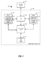
- the system 100 includes a multithreaded processor core 102 coupled to a non-core memory 104.
- the multithreaded processor core 102 includes a control logic circuit 106 coupled to a translation lookaside buffer (TLB) 108 and coupled to a TLB lock indicator 110.
- a first thread 112 is operatively coupled to the TLB 108 and to the control logic circuit 106.
- a second thread 114 is also operatively coupled to the TLB 108 and to the control logic circuit 106.
- two representative threads 112 and 114 are depicted in the system 100, it will be understood that the multithreaded processor core 102 may include any number or threads.
- the TLB 108 is a shared memory resource of the multithreaded processor core that is configured to receive requests from multiple threads, such as threads 112 and 114, to translate virtual addresses to physical addresses.
- the TLB 108 is configured to return a physical address that corresponds to a virtual address that is stored at the TLB 108.
- the TLB 108 is configured to signal a TLB miss event to the control logic circuit 106 when a requested virtual address is not found at the TLB 108.
- control logic circuit 106 is configured to receive one or more TLB miss event signals from the TLB 108 and to determine the status of the TLB lock indicator 110.
- the control logic circuit 106 may be configured to instruct the requesting thread 112 or 114 to save a current processing state and put the thread to sleep. Otherwise, when the TLB lock indicator 110 has an unlocked configuration, the control logic circuit 106 may be configured to lock the TLB lock indicator 110 and to concurrently instruct the requesting thread 112 or 114 to launch an exception handler to process the TLB miss event.
- TLB lock indicator 110 By locking the TLB lock indicator 110, other threads are prevented from modifying the TLB 108 so that the requesting thread can safely modify contents at the TLB 108 without the possibility of unpredictable behavior arising from simultaneous data write operations to an entry of the TLB 108 by multiple threads.
- the TLB lock indicator 110 may include one or more bits of a global status register of the multithreaded processor core 102.
- the TLB lock indicator 110 may be responsive to control signals from the control logic circuit 106.
- the TLB lock indicator 110 has a locked configuration to indicate that at least one thread 112 or 114 is performing a write operation at the TLB 108 and that access to the TLB by other threads is restricted. For example, other threads may be restricted to read-only access, no access, or a reduced level of access to the TLB 108 when the TLB lock indicator 110 is in a locked configuration.
- the TLB lock indicator 110 has an unlocked configuration, enabling normal access to the TLB 108 by the threads 112 and 114.
- the first thread 112 includes a sleep mode logic circuit 120 and an exception handler 122.
- the sleep mode logic circuit 120 may be configured to save a current state of the first thread 112, such as by saving a value of program counter (PC) (not shown), in response to a sleep instruction received from the control logic circuit 106.
- the sleep mode logic circuit 120 may be configured to store one or more values in a status register (not shown), such as a user mode status bit, an exception status bit, and data related to a last executed instruction packet that caused the TLB miss event.
- the exception handler 122 of the first thread 112 may fetch and execute instructions to handle an exception associated with a resource that is shared by the threads 112 and 114, and to unlock a hardware lock for the resource after the exception has been handled.
- the exception handler 122 includes logic and processor executable instructions to respond to a TLB miss event. For example, after the first thread 112 receives an instruction from the control logic circuit 106 to launch the exception handler 122, the exception handler 122 may set one or more status bits of the first thread 112 and may cause the first thread 112 to enter a supervisor mode and to load TLB miss exception handling instructions, such as instructions from the non-core memory 104.
- the exception handler 122 may be operable to fetch and execute instructions that enable recovery from the TLB miss event. For example, the exception handler 122 may process instructions causing the requested virtual address that triggered the TLB miss event to be located at a non-core memory resource, such as a page table. The exception handler 122 may write or program a translation of the virtual address into the TLB 108. The exception handler 122 may also be configured to execute a return instruction to exit an exception handling mode. The return instruction may be operable to return the thread 112 to a non-exception state and may request the control logic circuit 106 to unlock the TLB lock indicator 110. Alternatively, the return instruction may unlock the TLB lock indicator 110 upon return from the exception state without sending an unlock request to the control logic circuit 106.
- the second thread 114 includes a sleep mode logic circuit 130 and an exception handler 132.
- the second thread 114 including the sleep mode logic circuit 130 and the exception handler 132, operates substantially similarly to the first thread 112, including the sleep mode logic circuit 120 and the exception handler 122 of the first thread 112, respectively.
- multiple processing threads may send virtual address translation requests to the TLB 108.
- the control logic circuit 106 may lock the TLB 108 using the TLB lock indicator 110 to exclude other threads from modifying data at the TLB 108 while exception handling instructions respond to the TLB miss event.
- the TLB lock indicator 110 may include one or more bits in a global control register that may be set by the control logic circuit 106 to indicate that the TLB 108 is locked from access by the other threads.
- control logic circuit 106 is configured to set the TLB lock indicator 110 via a built-in hardware process and not by executing instructions of a software process, enabling a faster response to the TLB miss event, improved processor performance, and reduced vulnerability to malicious or poorly-behaved software applications. Additional performance benefits are enabled by using a global register bit in the multithreaded processor core 102 as the TLB lock indicator 110.
- the control logic circuit 106 may be configured to directly set, clear, and determine a status of the TLB lock indicator 110, so that a response to a TLB miss event may be significantly faster than storing or retrieving a lock indicator value such as a semaphore at the non-processor core memory 104.
- the control logic circuit 106 may instruct the thread 112 or 114 that generated the TLB miss event to launch the exception handler 122 or 132 to respond to the TLB miss event.
- the control logic circuit 106 may unlock the TLB lock indicator 110.
- the second thread 114 may also request a virtual address translation that results in a TLB miss event.
- the control logic circuit 106 may determine that the TLB lock indicator 110 is in a locked configuration, and may instruct the second thread 114 to go to sleep. For example, the control logic circuit 106 may instruct the second thread 114 to save a current state, to record an address of a last executed packet that caused the TLB miss event, and to enter a wait state during which the second thread 114 does not process instructions. Additional threads may encounter TLB miss events while the TLB lock indicator 110 remains locked and may also be put to sleep by the control logic circuit 106.
- the control logic circuit 106 When the control logic circuit 106 is informed that the TLB miss event associated with the first thread 112 has been handled, such as via a return instruction executed by the exception handler 122, the control logic circuit 106 unlocks the TLB lock indicator 110 and determines whether one or more processing threads are asleep due to the TLB 108 being locked. If so, the control logic circuit 106 awakens one or more of the sleeping threads, such as the second thread 114, to resume processing.
- the second thread 114 may be awakened and may replay the instruction packet that was executed immediately prior to the second thread 114 being put to sleep and that resulted in the TLB miss event.
- the replayed instruction packet may repeat a request for translation of a virtual address at the TLB 108.
- the virtual address translation requested by the second thread may potentially be stored in the TLB 108. If not, a second TLB miss event occurs, and in response the control logic circuit 106 resets the TLB lock indicator 110 to the locked configuration and instructs the exception handler 132 of the second thread 114 to begin processing instructions to handle the second TLB miss event.
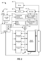
- the processing system 200 includes a memory 202 that is coupled to an instruction cache 210 via a bus interface 208.
- the processing system 200 also includes a data cache 212 that is coupled to the memory 202 via the bus interface 208.
- the instruction cache 210 is coupled to a sequencer 214 via a bus 211.
- the sequencer 214 can also receive general interrupts 216, which may be retrieved from an interrupt register (not shown).
- the instruction cache 210 is coupled to the sequencer 214 via a plurality of current instruction registers, which may be coupled to the bus 211 and associated with particular threads of the processing system 200.
- the processing system 200 is an interleaved multi-threaded processor including six threads.
- the bus 211 is a sixty-four (64)-bit bus and the sequencer 214 is configured to retrieve instructions from the memory 202 via instruction packets that include multiple instructions having a length of thirty-two (32) bits each.
- the bus 211 is coupled to a first instruction execution unit 218, a second instruction execution unit 220, a third instruction execution unit 222, and a fourth instruction execution unit 224.
- Each instruction execution unit 218, 220, 222, 224 can be coupled to a general register file 226 via a second bus 228.
- the general register file 226 can also be coupled to the sequencer 214 and to the data cache 212 via a third bus 230.
- the sequencer 214 includes or is otherwise coupled to a control logic circuit 270 that has access to thread-specific supervisor control registers 232 and to global control registers 234.
- the control logic circuit 270 is further coupled to a translation lookaside buffer (TLB) 272.
- TLB 272 is accessible to one or more of the execution units 218, 220, 222, and 224 to provide virtual-to-physical address translations and to signal a TLB miss event to the control logic circuit 270 when a requested address is not stored at the TLB 272.
- each thread-specific supervisor control register 232 includes multiple bit fields, such as a sleep field 280, an exception field 282, and a resume address field 284.
- the sleep field 280 may store one or more values or bit settings that indicate whether the associated thread is to transition between an active state and a sleep state.
- the exception field 282 may store one or more values to indicate a general exception or a particular type of exception, such as a TLB miss exception.
- the resume address field 284 may store an address or pointer to locate an instruction or execution packet to resume execution when the thread awakens.
- the thread when a thread is put to sleep in response to a TLB miss event that occurs while the TLB 272 is locked, the thread may store the address of the instruction that caused the TLB miss event to the resume address field 284.
- the associated thread when a value of the sleep field 280 transitions from a sleep indicator to an awake indicator, the associated thread may reload the instruction or execution packet indicated by the value stored at the resume address field 284 and begin execution.
- the global control registers 234 include one or more fields to indicate an order to awaken sleeping threads, such as a thread wake first-in-first-out buffer (FIFO) 290.
- the thread wake FIFO 290 may include one or more indicators to identify one or more of the processing threads of the system 200 that have been put to sleep in response to a TLB miss event occurring while a TLB lock 292 is in a locked configuration.
- the thread wake FIFO 290 may be configured to store thread indicators in an order that the threads are put to sleep, such that the control logic circuit 270 is operable to revive the sleeping threads in a matching order.
- the TLB lock 292 may include a single bit, the value of which indicates whether the TLB 272 is in a locked state or an unlocked state.
- control logic circuit 270 is configured to receive an indication of one or more TLB miss events at the TLB 272.
- the control logic circuit 270 may be configured to respond to a TLB miss event by first checking a status of the TLB lock 292. When the TLB lock 292 indicates that the TLB 272 is unlocked, the control logic circuit 270 may transition the TLB lock value 292 to a locked status and write a value to the exception field 282 of the corresponding thread-specific supervisor control register 232 to indicate that a TLB miss event has occurred and to instruct the thread to launch an exception handler.
- the control logic circuit 270 may further be configured to receive an instruction or signal from the exception handler when the TLB miss event has been handled, such as when the virtual address translation which caused the TLB miss event has been programmed to the TLB 272. In response, the control logic circuit 270 may be configured to unlock the TLB lock 292, and to check the thread wake FIFO 290 to determine whether one or more threads should be awakened. If so, the control logic circuit 270 is configured to awaken one or more of the threads, in order of storage at the thread wake FIFO 290, in an order of processing at the processing system 200, or in an order determined via one or more algorithms, such as based on a thread priority, by other mechanisms, or any combination thereof.
- the control logic circuit 270 may be configured to respond to a TLB miss event that occurs while the TLB lock 292 has a locked status, such as during exception handling by another thread that includes modifying at least one entry at the TLB 272.
- the control logic circuit 270 may be configured to write to the thread-specific supervisor control registers 232 to instruct the thread associated with the recent TLB miss event to store an address of a recent instruction or execution packet to the resume address field 284 and to go to sleep without initiating an exception handler associated with the recent TLB miss event.
- the control logic 270 may also be configured to not increment a program counter associated with the current thread when the current thread is put to sleep.
- the control logic circuit 270 may further be configured to store an identifier of the current thread at the thread wake FIFO 290.
- the lock indicator is a hardware lock, such as a register bit, associated with a translation lookaside buffer (TLB) that is shared between multiple processing threads.
- the method 300 may be performed by a control logic circuit of a multithreaded processor, such as the control logic circuit 106 of FIG. 1 or the control logic circuit 270 of FIG. 2 .
- a TLB miss event associated with a thread of a multi-threaded processor is received.
- the TLB miss event occurs at a software managed TLB.
- a TLB lock indicator is checked.
- the TLB lock indicator may include one or more register bits of a global control register, such as the TLB lock 292 of FIG. 2 . Proceeding to 306, a determination is made whether the TLB lock indicator is locked or unlocked.
- processing advances to 308, where the thread is put to sleep using the control logic circuit. Proceeding to 310, in a particular embodiment, a state of the exception handler causing the TLB lock is determined. Moving to 312, when the exception is determined to have not been handled, such as when the exception handler has not completed operations, processing may return to 310. When the exception is determined to be handled, in a particular embodiment, processing continues at 314, where the TLB lock indicator is transitioned from a locked state to an unlocked state. Proceeding to 316, after the TLB lock indicator transitions from the locked state to the unlocked state, execution of a packet that caused the TLB miss event may be replayed.
- processing advances to 318, where access by the thread to an exception handler associated with the TLB is allowed using a control logic circuit. Proceeding to 320, the TLB lock indicator is locked using the control logic circuit when access is allowed. In an illustrative embodiment, the exception handler sets the TLB lock indicator to a locked state.
- a result related to the TLB miss event may be calculated. For example, a virtual address translation for an address not located at the TLB may be determined by accessing a page table. Continuing to 324, in a particular embodiment, the result from the page table is programmed into the TLB.
- the TLB lock indicator is set to unlocked. Concurrently with unlocking the TLB lock indicator, processing returns from the exception handler, at 328. In a particular embodiment, the TLB lock indicator is automatically unlocked upon returning from the exception handler.
- FIG. 4 a particular illustrative embodiment of operations at a multithreaded processor with a lock indicator for a shared resource is depicted and generally designated 400.
- the diagram 400 illustrates operations associated with multiple threads, such as the representative threads: thread 0, thread 1, thread 2, and thread 3. Operations associated with a control unit and with a TLB lock indicator are also illustrated. A temporal relationship between operations is identified by six representative sequential time periods, labeled time 0 - time 5.
- the control unit may include a control logic circuit, such as the control logic circuit 108 of FIG. 1 or the control logic circuit 270 of FIG. 2 .
- TLB access is reserved for thread 0, and thread 0 encounters a TLB miss event 402.
- a signal 403 is sent to the control unit.
- the control unit processes a check lock operation 404.
- the check lock operation 404 determines whether the TLB lock indicator is in a locked or unlocked configuration. In the illustrative embodiment of FIG. 4 , the check lock operation 404 determines that the TLB lock indicator is in an unlocked state 406.
- control unit In response to determining that the TLB lock indicator is in the unlocked state 406, the control unit performs a set lock operation 408 to transition the TLB lock indicator to a locked state 410. In addition, the control unit sends a signal 409 to thread 0. In response to the signal 409, thread 0 launches a TLB miss exception handler 412.
- TLB access is reserved for thread 1.
- thread 0 is executing the TLB miss exception handler 412
- thread 1 performs a TLB access attempt that also results in a TLB miss event 414.
- the TLB miss event 414 is communicated to the control unit via a signal 415.
- the control unit performs a check lock operation 416 that determines that the TLB lock indicator is in a locked state 418. Because the TLB lock indicator is in the locked state 418, the control unit sends a signal 419 instructing thread 1 to sleep at 420.
- thread 1 saves a current state of the thread, such as by storing a program counter value, thread context values, other state information, or any combination thereof, and enters a state of reduced activity.
- TLB access is reserved for thread 2. While thread 0 continues to execute the TLB miss exception handler 412 and while thread 1 is asleep, thread 2 may perform a TLB access operation 422. Likewise, during time 3, TLB access is reserved for thread 3, which may perform a TLB access operation 424.
- TLB miss exception handler 412 of thread 0 finishes processing.
- TLB miss exception handler 412 may have accessed a page table, determined the virtual address translation that caused the TLB miss event 402, programmed the translation to the TLB, and executed a return instruction.
- a signal 425 informs the control unit that the TLB miss exception handler 412 has completed.
- the control unit performs a set lock operation 426 to transition the TLB lock indicator to an unlocked configuration 428.
- the control logic circuit may perform a check lock operation to determine when the TLB lock indicator is no longer in the locked state 418.
- the check lock operation may be engaged in periodically by the control unit, at designated intervals in response to designated events determined by the control unit, or automatically in response to signals indicating a completion of an exception handler, such as the signal 425.
- the TLB lock indicator is determined to be in an unlocked state 428.
- the control unit determines the next thread to awaken, at 432. As illustrated in FIG. 4 , thread 1 was the first thread put to sleep in response to a TLB miss while the TLB lock indicator was in the locked state 418. Therefore, at time 5, the control unit sends a signal 433 to awaken thread 1, in response to which thread 1 performs a wake operation and replays execution of instruction packet operation at 434.
- the wake and replay execution of packet operation 434 reloads the previous state of thread 1 that was saved prior to thread 1 being put to sleep at 420, and replays execution of the packet that generated the TLB miss event 414.
- the requested virtual address may have been loaded into the TLB by the TLB miss exception handler 412. Otherwise, another TLB miss event may result from replaying execution of the instruction packet at 434, to which the control unit may respond in a manner substantially similar as for the TLB miss 402.
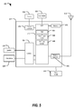
- FIG. 5 is a block diagram of a representative wireless communication device 500 that includes a multithreaded processor with a lock indicator for a shared resource.
- the wireless communications device 500 includes a multithreaded digital signal processor (DSP) 510 that includes a shared resource, such as a TLB 564, and a control logic circuit 566 coupled to the TLB 564 and further coupled to a TLB lock indicator 568.
- DSP digital signal processor
- the control logic circuit 566 is configured to operate in accordance with the systems and methods as described with respect to FIGs. 1-4 .
- FIG. 5 also shows a display controller 526 that is coupled to the digital signal processor 510 and to a display 528. Moreover, an input device 530 is coupled to the digital signal processor 510. Additionally, a memory 532 is coupled to the digital signal processor 510. A coder/decoder (CODEC) 534 can also be coupled to the digital signal processor 510. A speaker 536 and a microphone 538 can be coupled to the CODEC 534.
- CODEC coder/decoder
- FIG. 5 also indicates that a wireless controller 540 can be coupled to the digital signal processor 510 and to a wireless antenna 542.
- a power supply 544 is coupled to the on-chip system 522.
- the display 528, the input device 530, the speaker 536, the microphone 538, the wireless antenna 542, and the power supply 544 are external to the on-chip system 522. However, each is coupled to a component of the on-chip system 522.
- control logic circuit 566 need not be limited to controlling requests to access the TLB 564 in conjunction with the TLB lock indicator 568. Instead, the control logic circuit 566 may be operable to control access to one or more other shared resources, such as the display controller 526, the CODEC 534, the wireless controller 540, any other component of the DSP 510 or coupled to the DSP 510, or any combination thereof.
- the shared resource may be automatically locked before processing exception handling instructions associated with the shared resource by operation of control circuitry, such as the control logic circuit 106 of FIG. 1 and the control logic circuit 270 of FIG. 2 .
- the shared resource may also be unlocked by operation of control circuitry, such as the control logic circuit 106 of FIG. 1 and the control logic circuit 270 of FIG. 2 , or by operation of executable instructions, such as one or more instructions of an exception handler to unlock the shared resource.
- a software module may reside in RAM memory, flash memory, ROM memory, PROM memory, EPROM memory, EEPROM memory, registers, hard disk, a removable disk, a CD-ROM, or any other form of storage medium known in the art.
- An exemplary storage medium is coupled to the processor such that the processor can read information from, and write information to, the storage medium.
- the storage medium may be integral to the processor.
- the processor and the storage medium may reside in an ASIC.
- the ASIC may reside in a computing device or a user terminal.
- the processor and the storage medium may reside as discrete components in a computing device or user terminal.
Landscapes
- Engineering & Computer Science (AREA)
- Theoretical Computer Science (AREA)
- Software Systems (AREA)
- Physics & Mathematics (AREA)
- General Engineering & Computer Science (AREA)
- General Physics & Mathematics (AREA)
- Memory System Of A Hierarchy Structure (AREA)
Applications Claiming Priority (2)
| Application Number | Priority Date | Filing Date | Title |
|---|---|---|---|
| US11/949,284 US8140823B2 (en) | 2007-12-03 | 2007-12-03 | Multithreaded processor with lock indicator |
| PCT/US2008/085402 WO2009073722A1 (en) | 2007-12-03 | 2008-12-03 | Multithreaded processor with lock indicator |
Publications (2)
| Publication Number | Publication Date |
|---|---|
| EP2232370A1 EP2232370A1 (en) | 2010-09-29 |
| EP2232370B1 true EP2232370B1 (en) | 2015-11-04 |
Family
ID=40427128
Family Applications (1)
| Application Number | Title | Priority Date | Filing Date |
|---|---|---|---|
| EP08856823.3A Active EP2232370B1 (en) | 2007-12-03 | 2008-12-03 | Multithreaded processor with lock indicator |
Country Status (6)
| Country | Link |
|---|---|
| US (1) | US8140823B2 (enExample) |
| EP (1) | EP2232370B1 (enExample) |
| JP (3) | JP2011505647A (enExample) |
| KR (1) | KR101146359B1 (enExample) |
| CN (1) | CN101884029B (enExample) |
| WO (1) | WO2009073722A1 (enExample) |
Families Citing this family (53)
| Publication number | Priority date | Publication date | Assignee | Title |
|---|---|---|---|---|
| US8725992B2 (en) | 2008-02-01 | 2014-05-13 | International Business Machines Corporation | Programming language exposing idiom calls to a programming idiom accelerator |
| US8312458B2 (en) | 2008-02-01 | 2012-11-13 | International Business Machines Corporation | Central repository for wake-and-go mechanism |
| US8640141B2 (en) | 2008-02-01 | 2014-01-28 | International Business Machines Corporation | Wake-and-go mechanism with hardware private array |
| US8225120B2 (en) * | 2008-02-01 | 2012-07-17 | International Business Machines Corporation | Wake-and-go mechanism with data exclusivity |
| US8341635B2 (en) | 2008-02-01 | 2012-12-25 | International Business Machines Corporation | Hardware wake-and-go mechanism with look-ahead polling |
| US8880853B2 (en) * | 2008-02-01 | 2014-11-04 | International Business Machines Corporation | CAM-based wake-and-go snooping engine for waking a thread put to sleep for spinning on a target address lock |
| US8788795B2 (en) | 2008-02-01 | 2014-07-22 | International Business Machines Corporation | Programming idiom accelerator to examine pre-fetched instruction streams for multiple processors |
| US8452947B2 (en) | 2008-02-01 | 2013-05-28 | International Business Machines Corporation | Hardware wake-and-go mechanism and content addressable memory with instruction pre-fetch look-ahead to detect programming idioms |
| US8250396B2 (en) * | 2008-02-01 | 2012-08-21 | International Business Machines Corporation | Hardware wake-and-go mechanism for a data processing system |
| US8145849B2 (en) * | 2008-02-01 | 2012-03-27 | International Business Machines Corporation | Wake-and-go mechanism with system bus response |
| US8386822B2 (en) * | 2008-02-01 | 2013-02-26 | International Business Machines Corporation | Wake-and-go mechanism with data monitoring |
| US8015379B2 (en) * | 2008-02-01 | 2011-09-06 | International Business Machines Corporation | Wake-and-go mechanism with exclusive system bus response |
| US8127080B2 (en) * | 2008-02-01 | 2012-02-28 | International Business Machines Corporation | Wake-and-go mechanism with system address bus transaction master |
| US8516484B2 (en) | 2008-02-01 | 2013-08-20 | International Business Machines Corporation | Wake-and-go mechanism for a data processing system |
| US8612977B2 (en) | 2008-02-01 | 2013-12-17 | International Business Machines Corporation | Wake-and-go mechanism with software save of thread state |
| US8171476B2 (en) | 2008-02-01 | 2012-05-01 | International Business Machines Corporation | Wake-and-go mechanism with prioritization of threads |
| US8732683B2 (en) * | 2008-02-01 | 2014-05-20 | International Business Machines Corporation | Compiler providing idiom to idiom accelerator |
| US8316218B2 (en) | 2008-02-01 | 2012-11-20 | International Business Machines Corporation | Look-ahead wake-and-go engine with speculative execution |
| US8479166B2 (en) * | 2008-08-25 | 2013-07-02 | International Business Machines Corporation | Detecting locking discipline violations on shared resources |
| US8886919B2 (en) * | 2009-04-16 | 2014-11-11 | International Business Machines Corporation | Remote update programming idiom accelerator with allocated processor resources |
| US8082315B2 (en) * | 2009-04-16 | 2011-12-20 | International Business Machines Corporation | Programming idiom accelerator for remote update |
| US8230201B2 (en) | 2009-04-16 | 2012-07-24 | International Business Machines Corporation | Migrating sleeping and waking threads between wake-and-go mechanisms in a multiple processor data processing system |
| US8145723B2 (en) | 2009-04-16 | 2012-03-27 | International Business Machines Corporation | Complex remote update programming idiom accelerator |
| JP5428617B2 (ja) * | 2009-07-28 | 2014-02-26 | 富士通株式会社 | プロセッサ及び演算処理方法 |
| CN102486753B (zh) | 2009-11-30 | 2015-09-16 | 国际商业机器公司 | 构建及允许访问高速缓存的方法、设备及存储系统 |
| US8775836B2 (en) * | 2010-12-23 | 2014-07-08 | Intel Corporation | Method, apparatus and system to save processor state for efficient transition between processor power states |
| US9633407B2 (en) * | 2011-07-29 | 2017-04-25 | Intel Corporation | CPU/GPU synchronization mechanism |
| US9009410B2 (en) * | 2011-08-23 | 2015-04-14 | Ceva D.S.P. Ltd. | System and method for locking data in a cache memory |
| TWI454905B (zh) | 2011-09-30 | 2014-10-01 | Intel Corp | 在多核心平台中之受限制的啓動技術 |
| CN102426540B (zh) * | 2011-11-14 | 2013-06-05 | 苏州阔地网络科技有限公司 | 一种分布式即时通信软件中全局会话备份切换方法及装置 |
| CN103377086A (zh) * | 2012-04-27 | 2013-10-30 | 华为技术有限公司 | 用于异步多核系统操作共享资源的方法、装置及系统 |
| GB2499277B (en) | 2012-08-30 | 2014-04-02 | Imagination Tech Ltd | Global register protection in a multi-threaded processor |
| US9501332B2 (en) * | 2012-12-20 | 2016-11-22 | Qualcomm Incorporated | System and method to reset a lock indication |
| US10007323B2 (en) | 2012-12-26 | 2018-06-26 | Intel Corporation | Platform power consumption reduction via power state switching |
| US9361116B2 (en) | 2012-12-28 | 2016-06-07 | Intel Corporation | Apparatus and method for low-latency invocation of accelerators |
| US10140129B2 (en) | 2012-12-28 | 2018-11-27 | Intel Corporation | Processing core having shared front end unit |
| US20140189333A1 (en) * | 2012-12-28 | 2014-07-03 | Oren Ben-Kiki | Apparatus and method for task-switchable synchronous hardware accelerators |
| US9417873B2 (en) | 2012-12-28 | 2016-08-16 | Intel Corporation | Apparatus and method for a hybrid latency-throughput processor |
| US10346195B2 (en) | 2012-12-29 | 2019-07-09 | Intel Corporation | Apparatus and method for invocation of a multi threaded accelerator |
| US10114752B2 (en) * | 2014-06-27 | 2018-10-30 | International Business Machines Corporation | Detecting cache conflicts by utilizing logical address comparisons in a transactional memory |
| GB2529899B (en) * | 2014-09-08 | 2021-06-23 | Advanced Risc Mach Ltd | Shared Resources in a Data Processing Apparatus for Executing a Plurality of Threads |
| US9665376B2 (en) * | 2014-12-15 | 2017-05-30 | International Business Machines Corporation | Sharing program interrupt logic in a multithreaded processor |
| KR101638136B1 (ko) * | 2015-05-14 | 2016-07-08 | 주식회사 티맥스 소프트 | 멀티 스레드 구조에서 작업 분배 시 스레드 간 락 경쟁을 최소화하는 방법 및 이를 사용한 장치 |
| GB2539958B (en) * | 2015-07-03 | 2019-09-25 | Advanced Risc Mach Ltd | Data processing systems |
| US9864700B1 (en) * | 2016-08-17 | 2018-01-09 | Advanced Micro Devices, Inc. | Method and apparatus for power reduction in a multi-threaded mode |
| JP2018041204A (ja) | 2016-09-06 | 2018-03-15 | 東芝メモリ株式会社 | メモリ装置及び情報処理システム |
| KR101823129B1 (ko) * | 2016-11-24 | 2018-03-09 | 주식회사 실크로드소프트 | 컴퓨팅 장치의 리소스를 분배하는 컴퓨터 프로그램, 방법 및 장치 |
| KR102468506B1 (ko) * | 2016-11-24 | 2022-11-21 | 주식회사 실크로드소프트 | 컴퓨팅 장치의 리소스를 분배하는 컴퓨터 프로그램, 방법 및 장치 |
| CN107451257A (zh) * | 2017-07-31 | 2017-12-08 | 郑州云海信息技术有限公司 | 一种基于分布式文件系统的可维护性系统和方法 |
| US11361400B1 (en) | 2021-05-06 | 2022-06-14 | Arm Limited | Full tile primitives in tile-based graphics processing |
| US12013791B2 (en) | 2021-06-01 | 2024-06-18 | International Business Machines Corporation | Reset dynamic address translation protection instruction |
| US11593275B2 (en) | 2021-06-01 | 2023-02-28 | International Business Machines Corporation | Operating system deactivation of storage block write protection absent quiescing of processors |
| US11983538B2 (en) * | 2022-04-18 | 2024-05-14 | Cadence Design Systems, Inc. | Load-store unit dual tags and replays |
Family Cites Families (12)
| Publication number | Priority date | Publication date | Assignee | Title |
|---|---|---|---|---|
| US6754784B1 (en) * | 2000-02-01 | 2004-06-22 | Cirrus Logic, Inc. | Methods and circuits for securing encached information |
| US20010052053A1 (en) * | 2000-02-08 | 2001-12-13 | Mario Nemirovsky | Stream processing unit for a multi-streaming processor |
| US6742103B2 (en) * | 2000-08-21 | 2004-05-25 | Texas Instruments Incorporated | Processing system with shared translation lookaside buffer |
| US7159220B2 (en) * | 2001-09-28 | 2007-01-02 | Intel Corporation | Flexible acceleration of java thread synchronization on multiprocessor computers |
| US7234143B2 (en) * | 2002-06-20 | 2007-06-19 | Hewlett-Packard Development Company, L.P. | Spin-yielding in multi-threaded systems |
| AU2003250575A1 (en) * | 2002-08-07 | 2004-02-25 | Mmagix Technology Limited | Apparatus, method and system for a synchronicity independent, resource delegating, power and instruction optimizing processor |
| US7213093B2 (en) | 2003-06-27 | 2007-05-01 | Intel Corporation | Queued locks using monitor-memory wait |
| US7188229B2 (en) * | 2004-01-17 | 2007-03-06 | Sun Microsystems, Inc. | Method and apparatus for memory management in a multi-processor computer system |
| JP4576172B2 (ja) * | 2004-07-29 | 2010-11-04 | 富士通株式会社 | 演算処理装置,情報処理装置及び演算処理装置の制御方法 |
| US7398371B2 (en) * | 2005-06-23 | 2008-07-08 | Qualcomm Incorporated | Shared translation look-aside buffer and method |
| US7617380B2 (en) * | 2005-08-25 | 2009-11-10 | Broadcom Corporation | System and method for synchronizing translation lookaside buffer access in a multithread processor |
| US20070136725A1 (en) * | 2005-12-12 | 2007-06-14 | International Business Machines Corporation | System and method for optimized preemption and reservation of software locks |
-
2007
- 2007-12-03 US US11/949,284 patent/US8140823B2/en active Active
-
2008
- 2008-12-03 KR KR1020107014736A patent/KR101146359B1/ko not_active Expired - Fee Related
- 2008-12-03 CN CN200880119089.6A patent/CN101884029B/zh active Active
- 2008-12-03 WO PCT/US2008/085402 patent/WO2009073722A1/en not_active Ceased
- 2008-12-03 EP EP08856823.3A patent/EP2232370B1/en active Active
- 2008-12-03 JP JP2010537031A patent/JP2011505647A/ja active Pending
-
2013
- 2013-02-25 JP JP2013034561A patent/JP2013145568A/ja active Pending
-
2014
- 2014-06-04 JP JP2014116111A patent/JP2014197408A/ja active Pending
Also Published As
| Publication number | Publication date |
|---|---|
| CN101884029A (zh) | 2010-11-10 |
| JP2013145568A (ja) | 2013-07-25 |
| CN101884029B (zh) | 2014-09-03 |
| KR20100101629A (ko) | 2010-09-17 |
| KR101146359B1 (ko) | 2012-05-17 |
| WO2009073722A1 (en) | 2009-06-11 |
| JP2011505647A (ja) | 2011-02-24 |
| EP2232370A1 (en) | 2010-09-29 |
| JP2014197408A (ja) | 2014-10-16 |
| US8140823B2 (en) | 2012-03-20 |
| US20090144519A1 (en) | 2009-06-04 |
Similar Documents
| Publication | Publication Date | Title |
|---|---|---|
| EP2232370B1 (en) | Multithreaded processor with lock indicator | |
| JP4759273B2 (ja) | データ処理装置及び共用資源へのアクセス制御方法 | |
| JP5054665B2 (ja) | スリープ‐起動機構を用いた比較および交換動作 | |
| CN103814342B (zh) | 多核心计算装置的动态睡眠 | |
| US7328293B2 (en) | Queued locks using monitor-memory wait | |
| JP5538442B2 (ja) | リアルタイムマルチスレッドスケジューラおよびスケジューリング方法 | |
| US8539485B2 (en) | Polling using reservation mechanism | |
| US8578138B2 (en) | Enabling storage of active state in internal storage of processor rather than in SMRAM upon entry to system management mode | |
| JP2006031691A5 (enExample) | ||
| KR101671846B1 (ko) | 트랜잭셔널 메모리 동작들을 수행하도록 구성된 프로세서 | |
| JP2011507109A (ja) | マルチスレッド・プロセッサのための共有割込みコントローラ | |
| JPH05324471A (ja) | キャッシュ制御装置 | |
| JPWO2011096163A1 (ja) | 情報処理システム、排他制御方法および排他制御用プログラム | |
| WO2003040948A1 (en) | Computer and control method | |
| CN111767153B (zh) | 资源访问方法、装置及电子设备 | |
| US8438569B2 (en) | Broadcasting a condition to threads executing on a plurality of on-chip processors | |
| JPH06337839A (ja) | Cpu装置 |
Legal Events
| Date | Code | Title | Description |
|---|---|---|---|
| PUAI | Public reference made under article 153(3) epc to a published international application that has entered the european phase |
Free format text: ORIGINAL CODE: 0009012 |
|
| 17P | Request for examination filed |
Effective date: 20100702 |
|
| AK | Designated contracting states |
Kind code of ref document: A1 Designated state(s): AT BE BG CH CY CZ DE DK EE ES FI FR GB GR HR HU IE IS IT LI LT LU LV MC MT NL NO PL PT RO SE SI SK TR |
|
| AX | Request for extension of the european patent |
Extension state: AL BA MK RS |
|
| DAX | Request for extension of the european patent (deleted) | ||
| 17Q | First examination report despatched |
Effective date: 20130206 |
|
| RIC1 | Information provided on ipc code assigned before grant |
Ipc: G06F 12/10 20060101ALI20150331BHEP Ipc: G06F 9/30 20060101ALI20150331BHEP Ipc: G06F 9/52 20060101AFI20150331BHEP |
|
| GRAP | Despatch of communication of intention to grant a patent |
Free format text: ORIGINAL CODE: EPIDOSNIGR1 |
|
| INTG | Intention to grant announced |
Effective date: 20150522 |
|
| GRAS | Grant fee paid |
Free format text: ORIGINAL CODE: EPIDOSNIGR3 |
|
| GRAA | (expected) grant |
Free format text: ORIGINAL CODE: 0009210 |
|
| AK | Designated contracting states |
Kind code of ref document: B1 Designated state(s): AT BE BG CH CY CZ DE DK EE ES FI FR GB GR HR HU IE IS IT LI LT LU LV MC MT NL NO PL PT RO SE SI SK TR |
|
| REG | Reference to a national code |
Ref country code: GB Ref legal event code: FG4D |
|
| REG | Reference to a national code |
Ref country code: CH Ref legal event code: EP |
|
| REG | Reference to a national code |
Ref country code: AT Ref legal event code: REF Ref document number: 759640 Country of ref document: AT Kind code of ref document: T Effective date: 20151115 |
|
| REG | Reference to a national code |
Ref country code: IE Ref legal event code: FG4D |
|
| REG | Reference to a national code |
Ref country code: DE Ref legal event code: R096 Ref document number: 602008041044 Country of ref document: DE |
|
| REG | Reference to a national code |
Ref country code: NL Ref legal event code: MP Effective date: 20151104 |
|
| REG | Reference to a national code |
Ref country code: LT Ref legal event code: MG4D |
|
| REG | Reference to a national code |
Ref country code: AT Ref legal event code: MK05 Ref document number: 759640 Country of ref document: AT Kind code of ref document: T Effective date: 20151104 |
|
| PG25 | Lapsed in a contracting state [announced via postgrant information from national office to epo] |
Ref country code: HR Free format text: LAPSE BECAUSE OF FAILURE TO SUBMIT A TRANSLATION OF THE DESCRIPTION OR TO PAY THE FEE WITHIN THE PRESCRIBED TIME-LIMIT Effective date: 20151104 Ref country code: NL Free format text: LAPSE BECAUSE OF FAILURE TO SUBMIT A TRANSLATION OF THE DESCRIPTION OR TO PAY THE FEE WITHIN THE PRESCRIBED TIME-LIMIT Effective date: 20151104 Ref country code: LT Free format text: LAPSE BECAUSE OF FAILURE TO SUBMIT A TRANSLATION OF THE DESCRIPTION OR TO PAY THE FEE WITHIN THE PRESCRIBED TIME-LIMIT Effective date: 20151104 Ref country code: IT Free format text: LAPSE BECAUSE OF FAILURE TO SUBMIT A TRANSLATION OF THE DESCRIPTION OR TO PAY THE FEE WITHIN THE PRESCRIBED TIME-LIMIT Effective date: 20151104 Ref country code: NO Free format text: LAPSE BECAUSE OF FAILURE TO SUBMIT A TRANSLATION OF THE DESCRIPTION OR TO PAY THE FEE WITHIN THE PRESCRIBED TIME-LIMIT Effective date: 20160204 Ref country code: ES Free format text: LAPSE BECAUSE OF FAILURE TO SUBMIT A TRANSLATION OF THE DESCRIPTION OR TO PAY THE FEE WITHIN THE PRESCRIBED TIME-LIMIT Effective date: 20151104 Ref country code: IS Free format text: LAPSE BECAUSE OF FAILURE TO SUBMIT A TRANSLATION OF THE DESCRIPTION OR TO PAY THE FEE WITHIN THE PRESCRIBED TIME-LIMIT Effective date: 20160304 |
|
| PG25 | Lapsed in a contracting state [announced via postgrant information from national office to epo] |
Ref country code: LV Free format text: LAPSE BECAUSE OF FAILURE TO SUBMIT A TRANSLATION OF THE DESCRIPTION OR TO PAY THE FEE WITHIN THE PRESCRIBED TIME-LIMIT Effective date: 20151104 Ref country code: GR Free format text: LAPSE BECAUSE OF FAILURE TO SUBMIT A TRANSLATION OF THE DESCRIPTION OR TO PAY THE FEE WITHIN THE PRESCRIBED TIME-LIMIT Effective date: 20160205 Ref country code: FI Free format text: LAPSE BECAUSE OF FAILURE TO SUBMIT A TRANSLATION OF THE DESCRIPTION OR TO PAY THE FEE WITHIN THE PRESCRIBED TIME-LIMIT Effective date: 20151104 Ref country code: SE Free format text: LAPSE BECAUSE OF FAILURE TO SUBMIT A TRANSLATION OF THE DESCRIPTION OR TO PAY THE FEE WITHIN THE PRESCRIBED TIME-LIMIT Effective date: 20151104 Ref country code: PT Free format text: LAPSE BECAUSE OF FAILURE TO SUBMIT A TRANSLATION OF THE DESCRIPTION OR TO PAY THE FEE WITHIN THE PRESCRIBED TIME-LIMIT Effective date: 20160304 Ref country code: BE Free format text: LAPSE BECAUSE OF NON-PAYMENT OF DUE FEES Effective date: 20151231 Ref country code: PL Free format text: LAPSE BECAUSE OF FAILURE TO SUBMIT A TRANSLATION OF THE DESCRIPTION OR TO PAY THE FEE WITHIN THE PRESCRIBED TIME-LIMIT Effective date: 20151104 Ref country code: AT Free format text: LAPSE BECAUSE OF FAILURE TO SUBMIT A TRANSLATION OF THE DESCRIPTION OR TO PAY THE FEE WITHIN THE PRESCRIBED TIME-LIMIT Effective date: 20151104 |
|
| PG25 | Lapsed in a contracting state [announced via postgrant information from national office to epo] |
Ref country code: CZ Free format text: LAPSE BECAUSE OF FAILURE TO SUBMIT A TRANSLATION OF THE DESCRIPTION OR TO PAY THE FEE WITHIN THE PRESCRIBED TIME-LIMIT Effective date: 20151104 |
|
| REG | Reference to a national code |
Ref country code: CH Ref legal event code: PL |
|
| REG | Reference to a national code |
Ref country code: DE Ref legal event code: R097 Ref document number: 602008041044 Country of ref document: DE |
|
| PG25 | Lapsed in a contracting state [announced via postgrant information from national office to epo] |
Ref country code: RO Free format text: LAPSE BECAUSE OF FAILURE TO SUBMIT A TRANSLATION OF THE DESCRIPTION OR TO PAY THE FEE WITHIN THE PRESCRIBED TIME-LIMIT Effective date: 20151104 Ref country code: DK Free format text: LAPSE BECAUSE OF FAILURE TO SUBMIT A TRANSLATION OF THE DESCRIPTION OR TO PAY THE FEE WITHIN THE PRESCRIBED TIME-LIMIT Effective date: 20151104 Ref country code: SK Free format text: LAPSE BECAUSE OF FAILURE TO SUBMIT A TRANSLATION OF THE DESCRIPTION OR TO PAY THE FEE WITHIN THE PRESCRIBED TIME-LIMIT Effective date: 20151104 Ref country code: EE Free format text: LAPSE BECAUSE OF FAILURE TO SUBMIT A TRANSLATION OF THE DESCRIPTION OR TO PAY THE FEE WITHIN THE PRESCRIBED TIME-LIMIT Effective date: 20151104 |
|
| PLBE | No opposition filed within time limit |
Free format text: ORIGINAL CODE: 0009261 |
|
| STAA | Information on the status of an ep patent application or granted ep patent |
Free format text: STATUS: NO OPPOSITION FILED WITHIN TIME LIMIT |
|
| REG | Reference to a national code |
Ref country code: IE Ref legal event code: MM4A |
|
| PG25 | Lapsed in a contracting state [announced via postgrant information from national office to epo] |
Ref country code: MC Free format text: LAPSE BECAUSE OF FAILURE TO SUBMIT A TRANSLATION OF THE DESCRIPTION OR TO PAY THE FEE WITHIN THE PRESCRIBED TIME-LIMIT Effective date: 20151104 |
|
| REG | Reference to a national code |
Ref country code: FR Ref legal event code: ST Effective date: 20160831 |
|
| 26N | No opposition filed |
Effective date: 20160805 |
|
| PG25 | Lapsed in a contracting state [announced via postgrant information from national office to epo] |
Ref country code: IE Free format text: LAPSE BECAUSE OF NON-PAYMENT OF DUE FEES Effective date: 20151203 Ref country code: LI Free format text: LAPSE BECAUSE OF NON-PAYMENT OF DUE FEES Effective date: 20151231 Ref country code: CH Free format text: LAPSE BECAUSE OF NON-PAYMENT OF DUE FEES Effective date: 20151231 |
|
| PG25 | Lapsed in a contracting state [announced via postgrant information from national office to epo] |
Ref country code: SI Free format text: LAPSE BECAUSE OF FAILURE TO SUBMIT A TRANSLATION OF THE DESCRIPTION OR TO PAY THE FEE WITHIN THE PRESCRIBED TIME-LIMIT Effective date: 20151104 Ref country code: FR Free format text: LAPSE BECAUSE OF NON-PAYMENT OF DUE FEES Effective date: 20160104 |
|
| PG25 | Lapsed in a contracting state [announced via postgrant information from national office to epo] |
Ref country code: BE Free format text: LAPSE BECAUSE OF FAILURE TO SUBMIT A TRANSLATION OF THE DESCRIPTION OR TO PAY THE FEE WITHIN THE PRESCRIBED TIME-LIMIT Effective date: 20151104 |
|
| PG25 | Lapsed in a contracting state [announced via postgrant information from national office to epo] |
Ref country code: BG Free format text: LAPSE BECAUSE OF FAILURE TO SUBMIT A TRANSLATION OF THE DESCRIPTION OR TO PAY THE FEE WITHIN THE PRESCRIBED TIME-LIMIT Effective date: 20151104 Ref country code: HU Free format text: LAPSE BECAUSE OF FAILURE TO SUBMIT A TRANSLATION OF THE DESCRIPTION OR TO PAY THE FEE WITHIN THE PRESCRIBED TIME-LIMIT; INVALID AB INITIO Effective date: 20081203 |
|
| PG25 | Lapsed in a contracting state [announced via postgrant information from national office to epo] |
Ref country code: CY Free format text: LAPSE BECAUSE OF FAILURE TO SUBMIT A TRANSLATION OF THE DESCRIPTION OR TO PAY THE FEE WITHIN THE PRESCRIBED TIME-LIMIT Effective date: 20151104 |
|
| PG25 | Lapsed in a contracting state [announced via postgrant information from national office to epo] |
Ref country code: TR Free format text: LAPSE BECAUSE OF FAILURE TO SUBMIT A TRANSLATION OF THE DESCRIPTION OR TO PAY THE FEE WITHIN THE PRESCRIBED TIME-LIMIT Effective date: 20151104 Ref country code: MT Free format text: LAPSE BECAUSE OF FAILURE TO SUBMIT A TRANSLATION OF THE DESCRIPTION OR TO PAY THE FEE WITHIN THE PRESCRIBED TIME-LIMIT Effective date: 20151104 |
|
| PG25 | Lapsed in a contracting state [announced via postgrant information from national office to epo] |
Ref country code: LU Free format text: LAPSE BECAUSE OF NON-PAYMENT OF DUE FEES Effective date: 20151203 |
|
| REG | Reference to a national code |
Ref country code: DE Ref legal event code: R082 Ref document number: 602008041044 Country of ref document: DE Representative=s name: MAUCHER JENKINS PATENTANWAELTE & RECHTSANWAELT, DE |
|
| PGFP | Annual fee paid to national office [announced via postgrant information from national office to epo] |
Ref country code: DE Payment date: 20241111 Year of fee payment: 17 |
|
| PGFP | Annual fee paid to national office [announced via postgrant information from national office to epo] |
Ref country code: GB Payment date: 20241114 Year of fee payment: 17 |