EP2228596A1 - Optische Halbleitervorrichtung, Aufnahme und optische Halbleitereinheit - Google Patents
Optische Halbleitervorrichtung, Aufnahme und optische Halbleitereinheit Download PDFInfo
- Publication number
- EP2228596A1 EP2228596A1 EP20100153625 EP10153625A EP2228596A1 EP 2228596 A1 EP2228596 A1 EP 2228596A1 EP 20100153625 EP20100153625 EP 20100153625 EP 10153625 A EP10153625 A EP 10153625A EP 2228596 A1 EP2228596 A1 EP 2228596A1
- Authority
- EP
- European Patent Office
- Prior art keywords
- optical semiconductor
- main body
- socket
- electrode portion
- semiconductor device
- Prior art date
- Legal status (The legal status is an assumption and is not a legal conclusion. Google has not performed a legal analysis and makes no representation as to the accuracy of the status listed.)
- Granted
Links
Images


Classifications
-
- G—PHYSICS
- G06—COMPUTING OR CALCULATING; COUNTING
- G06F—ELECTRIC DIGITAL DATA PROCESSING
- G06F30/00—Computer-aided design [CAD]
- G06F30/30—Circuit design
- G06F30/39—Circuit design at the physical level
- G06F30/392—Floor-planning or layout, e.g. partitioning or placement
-
- H—ELECTRICITY
- H01—ELECTRIC ELEMENTS
- H01R—ELECTRICALLY-CONDUCTIVE CONNECTIONS; STRUCTURAL ASSOCIATIONS OF A PLURALITY OF MUTUALLY-INSULATED ELECTRICAL CONNECTING ELEMENTS; COUPLING DEVICES; CURRENT COLLECTORS
- H01R12/00—Structural associations of a plurality of mutually-insulated electrical connecting elements, specially adapted for printed circuits, e.g. printed circuit boards [PCB], flat or ribbon cables, or like generally planar structures, e.g. terminal strips, terminal blocks; Coupling devices specially adapted for printed circuits, flat or ribbon cables, or like generally planar structures; Terminals specially adapted for contact with, or insertion into, printed circuits, flat or ribbon cables, or like generally planar structures
- H01R12/70—Coupling devices
- H01R12/7076—Coupling devices for connection between PCB and component, e.g. display
-
- H—ELECTRICITY
- H01—ELECTRIC ELEMENTS
- H01R—ELECTRICALLY-CONDUCTIVE CONNECTIONS; STRUCTURAL ASSOCIATIONS OF A PLURALITY OF MUTUALLY-INSULATED ELECTRICAL CONNECTING ELEMENTS; COUPLING DEVICES; CURRENT COLLECTORS
- H01R12/00—Structural associations of a plurality of mutually-insulated electrical connecting elements, specially adapted for printed circuits, e.g. printed circuit boards [PCB], flat or ribbon cables, or like generally planar structures, e.g. terminal strips, terminal blocks; Coupling devices specially adapted for printed circuits, flat or ribbon cables, or like generally planar structures; Terminals specially adapted for contact with, or insertion into, printed circuits, flat or ribbon cables, or like generally planar structures
- H01R12/70—Coupling devices
- H01R12/71—Coupling devices for rigid printing circuits or like structures
- H01R12/712—Coupling devices for rigid printing circuits or like structures co-operating with the surface of the printed circuit or with a coupling device exclusively provided on the surface of the printed circuit
- H01R12/716—Coupling device provided on the PCB
-
- H—ELECTRICITY
- H01—ELECTRIC ELEMENTS
- H01R—ELECTRICALLY-CONDUCTIVE CONNECTIONS; STRUCTURAL ASSOCIATIONS OF A PLURALITY OF MUTUALLY-INSULATED ELECTRICAL CONNECTING ELEMENTS; COUPLING DEVICES; CURRENT COLLECTORS
- H01R13/00—Details of coupling devices of the kinds covered by groups H01R12/70 or H01R24/00 - H01R33/00
- H01R13/02—Contact members
- H01R13/20—Pins, blades, or sockets shaped, or provided with separate member, to retain co-operating parts together
-
- H—ELECTRICITY
- H05—ELECTRIC TECHNIQUES NOT OTHERWISE PROVIDED FOR
- H05K—PRINTED CIRCUITS; CASINGS OR CONSTRUCTIONAL DETAILS OF ELECTRIC APPARATUS; MANUFACTURE OF ASSEMBLAGES OF ELECTRICAL COMPONENTS
- H05K3/00—Apparatus or processes for manufacturing printed circuits
- H05K3/30—Assembling printed circuits with electric components, e.g. with resistors
- H05K3/301—Assembling printed circuits with electric components, e.g. with resistors by means of a mounting structure
-
- H—ELECTRICITY
- H05—ELECTRIC TECHNIQUES NOT OTHERWISE PROVIDED FOR
- H05K—PRINTED CIRCUITS; CASINGS OR CONSTRUCTIONAL DETAILS OF ELECTRIC APPARATUS; MANUFACTURE OF ASSEMBLAGES OF ELECTRICAL COMPONENTS
- H05K2201/00—Indexing scheme relating to printed circuits covered by H05K1/00
- H05K2201/10—Details of components or other objects attached to or integrated in a printed circuit board
- H05K2201/10007—Types of components
- H05K2201/10106—Light emitting diode [LED]
-
- H—ELECTRICITY
- H05—ELECTRIC TECHNIQUES NOT OTHERWISE PROVIDED FOR
- H05K—PRINTED CIRCUITS; CASINGS OR CONSTRUCTIONAL DETAILS OF ELECTRIC APPARATUS; MANUFACTURE OF ASSEMBLAGES OF ELECTRICAL COMPONENTS
- H05K2201/00—Indexing scheme relating to printed circuits covered by H05K1/00
- H05K2201/10—Details of components or other objects attached to or integrated in a printed circuit board
- H05K2201/10227—Other objects, e.g. metallic pieces
- H05K2201/10325—Sockets, i.e. female type connectors comprising metallic connector elements integrated in, or bonded to a common dielectric support
Definitions
- This invention relates to an optical semiconductor device, a socket for mounting the optical semiconductor device thereto, and an optical semiconductor unit.
- LED Light Emitting Diode
- the LED device generates less heat as compared to a common light source using a filament or the like.
- a driving current is increased and, as a result, heat generated from an LED is increasing. This brings about a problem that the heat generation increases a temperature of the LED device to cause deterioration of the LED device.
- Patent Document 3 proposes an LED socket having a structure in which an entire substrate with an LED device is brought into tight contact with a heat sink to be cooled, as disclosed in JP-A-2004-265626 (Patent Document 3).
- an object of the present invention to provide an optical semiconductor device which is easily replaceable and which has an electrode portion of a structure capable of efficiently transferring heat generated therein without increasing the size of the device.
- a first aspect of the present invention is an optical semiconductor device comprising: a main body to which an optical semiconductor is mounted; and an electrode portion formed on the main body,the electrode portion having a block shape as an outer shape.
- a second aspect of the present invention is a socket mounting the optical semiconductor device according to the first aspect of the present invention, wherein the socket has a total thermal property data not less than the thermal property data of the main body.
- a third aspect of the present invention is an optical semiconductor unit comprising; an optical semiconductor device comprising a main body to which an optical semiconductor is mounted and an electrode portion formed on the main body having a block shape as an outer shape; and a socket mounting the optical semiconductor device, wherein the socket has a total thermal property data not less than the thermal property data of the main body.
- a fourth aspect of the present invention is a method of designing an optical semiconductor device having a main body to which an optical semiconductor is mounted, and an electrode portion formed on the main body, the method comprising: (a) defining an input power supplied to the optical semiconductor and a junction temperature of the optical semiconductor; (b) obtaining a first graph showing a relationship between a volume of the main body and a temperature of the optical semiconductor at the defined input power and a second graph showing a relationship between a volume of the electrode portion and the temperature of the optical semiconductor at the defined input power; (c) calculating, from the first and the second graphs, the volumes of the main body and the electrode portion at the junction temperature; and (d) designing the main body and the electrode portion so that the main body and the electrode portion have the volumes calculated in (c).
- a fifth aspect of the present invention is a method of designing a socket having a plurality of socket terminals connected to an optical semiconductor device having an optical semiconductor, the method comprising: (e) defining an input power supplied to the optical semiconductor and a junction temperature of the optical semiconductor; (f) obtaining a third graph showing a relationship between a volume of the socket terminals and a temperature of the optical semiconductor at the defined input power; (g) calculating, from the third graph, the volume of the socket terminals at the junction temperature; and (h) designing the socket terminals so that the socket terminals have the volume calculated in (g).
- the electrode portion has a block shape in external appearance.
- heat generated in the optical semiconductor device is transferred through an electrode to a substrate to cool the optical semiconductor device. Therefore, it is possible to provide an optical semiconductor device which is easily replaceable and which has an electrode portion of a structure capable of efficiently transferring heat generated in the optical semiconductor device without increasing the size of the device.
- the optical semiconductor unit 1 comprises an LED device 3 as an optical semiconductor device provided with an LED 9, and a socket 5 to which the LED device 3 is mounted.
- the socket 5 is fixed to a substrate 6a by a solder 6b.
- the LED device 3 As one component of the optical semiconductor unit 1 comprising the LED device 3 and the socket 5, the LED device 3 will first be described with reference to Figs. 2 to 3B .
- the LED device 3 comprises a main body 7 to which the LED 9 is mounted.
- a ceramic material such as alumina (Al 2 O 3 ), aluminum nitride (AIN), or silicon nitride (SiN), is desirably used. This is because thermal property data can be increased by the use of the ceramic material as compared to an organic material which has been used as a material for the main body.
- the main body 7 has, on a rear side thereof, a first surface 11 having a rectangular (square) planar shape.
- first surface 11 having a rectangular (square) planar shape.
- block-shaped electrode portions 13a and 13b are connected through bonding portions 23a and 23b, respectively.
- the electrode portions 13a and 13b are formed of, for example, copper (Cu) plated with gold (Au).
- the bonding portions 23a and 23b are formed of, for example, a soft solder, a silver (Ag) solder, or the like.
- each of the electrode portions 13a and 13b has a bar-like shape and is connected to the main body 7 along its longitudinal direction.
- the electrode portions 13a and 13b are disposed along (in parallel to) a pair of sides 8 of the first surface 11.
- the electrode portions 13a and 13b are electrically connected to the LED 9 through an internal conductor (for example, Cu plated with Ag, Au, or the like) which is disposed inside the main body 7 but which is not shown in the figure.
- the electrode portions 13a and 13b have both a power-feeding function of feeding an electric power to the LED 9 and a heat-transferring function of transferring heat generated by light emission of the LED 9 to the socket 5.
- the heat transferred to the socket 5 is dissipated or radiated by the substrate 6a, a heat sink (not shown) disposed on the substrate 6a or the like.
- Each of the electrode portions 13a and 13b has a bar-like shape. With this structure, it is possible to reliably connect the LED device 3 and the socket 5 to each other, as will later be described. In addition, it is possible to increase the thermal property data of the electrode portions. As a result, the heat generated by the LED 9 can efficiently be transferred.
- the electrode portions 13a and 13b are provided with concave portions 25a and 25b on lateral sides thereof (in the longitudinal direction), respectively. A function of the concave portions 25a and 25b will later be described.
- the electrode portions 13a and 13b do not protrude from the first surface 11 as shown in Fig. 3B .
- a total thermal property data of the electrode portions 13a and 13b is desirably not less than a thermal property data of the main body 7. The reason is as follows.
- the heat generated when the LED 9 emits light is transferred through the main body 7, the electrode portions 13a and 13b, and socket terminals 19a and 19b of the socket 5 (which will be described later) in this order, and finally dissipated or radiated from the substrate 6a, or the heat sink (not shown) disposed on the substrate 6a or the like.
- the thermal property data of the electrode portions 13a and 13b is smaller than the thermal property data of the main body 7, a transfer rate of the heat generated when the LED 9 is operated is limited in the electrode portions 13a and 13b (i.e., the electrode portions 13a and 13b become a so-called "heat reservoir"). This prevents heat dissipation or radiation and causes deterioration of the LED 9.
- the total thermal property data of the electrode portions 13a and 13b is not less than the thermal property data of the main body 7.
- the total thermal property data of the electrode portions 13a and 13b is desirably within five times the thermal property data of the main body 7, more desirably within two times. This is because, if the total thermal property data of the electrode portions 13a and 13b exceeds five times the thermal property data of the main body 7, the total thermal property data of the electrode portions 13a and 13b becomes unnecessarily large and the electrode portions 13a and 13b are increased in size.
- the socket 5 comprises a housing 15 formed of an insulator.
- the housing 15 has concave portions 17a and 17b corresponding in shape to the electrode portions 13a and 13b, respectively.
- the concave portions 17a and 17b have a plurality of socket terminals 19a and 19b formed therein, respectively.
- FIG. 2 eleven socket terminals 19a and eleven socket terminals 19b are shown.
- the socket terminals 19a and 19b comprise U-shaped portions 31 a and 31 b having a U shape and inverse U-shaped portions 33a and 33b having an inverse U shape and extending from one ends of the U-shaped portions 31 a and 31 b, respectively.
- the U-shaped portions 31 a and 31 b are press-fitted or insert-molded into the concave portions 17a and 17b, respectively. As a result, the socket terminals 19a and 19b are fixed to the housing 15.
- the inverse U-shaped portions 33a and 33b have ends fixed to the substrate 6a by the solder 6b.
- the other ends of the U-shaped portions 31 a and 31 b have protruding portions 35a and 35b protruding inward from the U shapes, respectively.
- the socket terminals 19a and 19b are formed of metal, such as oxygen-free copper or phosphor bronze, plated with Au, Pd (palladium), Ag, Sn (tin), or the like. At least the U-shaped portions 31 a and 31b comprise metal springs.
- the socket terminals 19a and 19b desirably have a thermal conductivity as high as possible. This is because the socket terminals having a high thermal conductivity can efficiently transfer the heat generated by light emission of the LED 9 to the substrate 6a. In addition, the socket terminals having a high thermal conductivity dissipate or radiate heat to atmosphere by themselves and further contribute to heat dissipation or radiation.
- the socket terminals 19a and 19b desirably have a total thermal property data not less than the thermal property data of the main body 7 of the LED device 3. This is because, in the manner similar to that described in connection with the total thermal property data of the electrode portions 13a and 13b, the socket terminals 19a and 19b are prevented from becoming a heat reservoir.
- the LED device 3 is moved in a direction depicted by an arrow C in Fig. 2 to insert the electrode portions 13a and 13b into the concave portions 17a and 17b, respectively.
- the electrode portions 13a and 13b press and expand the U-shaped portions 31 a and 31 b of the socket terminals 19a and 19b, respectively.
- the U-shaped portions 31 a and 31 b comprising the metal springs exert a repelling force.
- the electrode portions 13a and 13b are electrically connected to the socket terminals 19a and 19b, respectively.
- the protruding portions 35a and 35b (see Fig. 4B ) of the socket terminals 19a and 19b are inserted into the concave portions 25a and 25b (see Fig. 3A ) of the electrode portions 13a and 13b, respectively.
- the electrode portions 13a and 13b are engaged with and fixed to the socket terminals 19a and 19b, respectively.
- the LED device 3 and the socket 5 are connected to each other by inserting the LED device 3 from an upper side of the socket 5 and fixing the bar-like electrode portions 13a and 13b by the repelling force of the U-shaped portions 31 a and 31 b comprising the metal springs.
- the metal springs serve to provide electrical connection, thermal connection, and mechanical fixation.
- the optical semiconductor unit 1 has a structure capable of efficiently transferring the heat generated by the LED 9 without increasing the LED device 3 in size.
- the LED device 3 and the socket 5 can be connected to each other only by inserting the LED device 3 into the socket 5. Accordingly, the LED device 3 can easily be replaced.
- the LED device 3 may be automatically mounted using a mounter or the like.
- Each of the electrode portions 13a and 13b has a block shape and a number of the socket terminals 19a and 19b are provided. With this structure, the electrode portions 13a and 13b and the socket terminals 19a and 19b can more reliably be connected and the heat can efficiently be transferred.
- the socket terminals 19a and 19b are provided with the protruding portions 35a and 35b, respectively, while the electrode portions 13a and 13b are provided with the concave portions 25a and 25b, respectively.
- the electrode portions 13a and 13b and the socket terminals 19a and 19b can more reliably be connected (1) thermally, (2) electrically, and (3) mechanically.
- the optical semiconductor unit 1 shown in Fig. 1 may be connected to the substrate 6a by connecting the socket terminals 19a and 19b of the socket 5 to the substrate 6a by the solder 6b and, thereafter, inserting the LED device 3 into the socket 5. However, if the bonding portions 23a and 23b have a melting point higher than that of the solder 6b, the optical semiconductor unit 1 may be connected to the substrate 6a after the LED device 3 is preliminarily inserted into the socket 5 and taped thereto.
- the socket 5 is provided with a hole 21 having a rectangular planar shape and formed between the concave portions 17a and 17b.
- the hole 21 may not be formed. However, if the hole 21 is filled with a material having a thermal conductivity higher than that of the housing 15, it is expected to achieve higher heat radiation. Further, if the hole 21 has through-hole portions (vent holes 21 a and 21 b) penetrating through the housing 15 to the outside in a longitudinal direction of the rectangular shape, the hole 21 may also function as a ventilation hole.
- the total thermal property data of the electrode portions 13a and 13b or the total thermal property data of the socket terminals 19a and 19b is not less than the thermal property data of the main body 7.
- the total thermal property data of the electrode portions 13a and 13b or the socket terminals 19a and 19b is desirably equal to the thermal property data of the main body 7.
- various values are defined, for example, an input power supplied to the LED 9, an upper limit junction temperature of the LED 9, a thermal conductivity and a volume of each of the main body 7, the substrate 6a, the LED 9, the electrode portions 13a and 13b, and the socket terminals 19a and 19b, an ambient temperature, a heat transfer coefficient of air, and so on. Then, a thermal property data is calculated.
- the thermal property data of the main body 7, the electrode portions 13a and 13b, and the socket terminals 19a and 19b are equal to one another.
- dimensions and shapes of the main body 7, the electrode portions 13a and 13b, and the socket terminals 19a and 19b are designed so that the main body 7, the electrode portions 13a and 13b, and the socket terminals 19a and 19b have the volumes as mentioned above.
- the total thermal property data of the electrode portions 13a and 13b or the socket terminals 19a and 19b is required to be not less than the thermal property data of the main body 7. Therefore, the electrode portions 13a and 13b or the socket terminals 19a and 19b may have a volume greater than the volume at the defined junction temperature. In other words, the volume of the electrode portions 13a and 13b or the socket terminals 19a and 19b must be equal to or greater than the volume at the defined junction temperature.
- the foregoing is the method of designing the main body 7 and the electrode portions 13a and 13b of the LED device 3 and the socket terminals 19a and 19b.
- the optical semiconductor unit 1 comprises the LED device 3 provided with the LED 9, and the socket 5 for mounting the LED device 3 thereon.
- the LED device 3 and the socket 5 are connected to each other by fixing the block-shaped electrode portions 13a and 13b of the LED device 3 with the repelling force of the socket terminals 19a and 19b of the socket 5.
- the LED device 3 and the socket 5 may easily be connected to each other manually or automatically and the LED device 3 is easily replaceable.
- the total thermal property data of the electrode portions 13a and 13b or the socket terminals 19a and 19b is not less than the thermal property data of the main body 7 of the LED device 3. As a result, the electrode portions 13a and 13b or the socket terminals 19a and 19b are prevented from becoming a heat reservoir.
- the socket terminals 19a and 19b are provided with the protruding portions 35a and 35b, respectively, while the electrode portions 13a and 13b are provided with the concave portions 25a and 25b, respectively. With this structure, it is possible to reliably connect the electrode portions 13a and 13b and the socket terminals 19a and 19b.
- each of the electrode portions in the first embodiment is divided in an axial direction into a plurality of electrode members of a rectangular prism shape.
- an LED device 3a comprises electrode portions 71 a and 71 b each of which is divided in the axial direction into the plurality of electrode members of a rectangular prism shape.
- the LED device 3a has an electrode structure in which each of the electrode portions 71 a and 71 b is divided into a plurality of electrode members in the axial direction. With this structure, the LED device 3a is applicable to a case where a multicolor LED or a plurality of monocolor LEDs are mounted.
- the LED device 3a having six electrode members as shown in Fig. 5 is required, for example, in case where the LED device 3a comprises three LED elements (R, G, B) (in this case, anode and cathode terminals are necessary for each color and, therefore, six electrode members are required in total).
- each of the electrode portions in the first embodiment is formed of a plate material having a hook shape in section perpendicular to an axial direction.
- an LED device 3b comprises electrode portions 41 a and 41 b each of which has a hook shape in section perpendicular to the axial direction (longitudinal direction).
- the above-mentioned shape is obtained by, for example, pressing the plate material.
- the electrode portion may have a hollow shape, for example, with a hook shape in section, as long as an outer shape is a block shape.
- each of the electrode portions has a hook shape in section but may have a U shape or the like in section.
- each of the electrode portions 41 a and 41 b of the LED device 3b has the hook shape in section perpendicular to the axial direction (longitudinal direction) and exhibits an effect similar to that of the first embodiment.
- a socket 5a has four socket terminals 43a and four socket terminals 43b each of which is increased in width as compared to the first embodiment.
- the socket 5a comprises the socket terminals 43a and 43b in the concave portions 17a and 17b, respectively.
- the four socket terminals 43a and the four socket terminals 43b are formed and each of the socket terminals has a width greater than that of each of the socket terminals 19a and 19b in the first embodiment.
- the number and the width of the socket terminals are not limited to those in the first embodiment.
- the socket terminals increased in width increase a contact area with the electrode portions 13a and 13b and, therefore, contribute to heat dissipation or radiation. Further, in proportion to the width of the socket terminal, the repelling force of the spring is also increased. Accordingly, it is possible to achieve a stronger fixing strength.
- each of the socket terminals 43a and 43b of the socket 5a has a width greater than that of each of the socket terminals 19a and 19b in the first embodiment. Consequently, the fourth embodiment is more effective in heat dissipation or radiation and in fixing strength as compared to the first embodiment.
- volumes of the main body 7 and the electrode portions 13a and 13b of the LED device 3 were calculated so as to optimize the thermal property data.
- the LED 9 had a size of 1 mm square and a height of 0.1mm.
- a thermal conductivity of the LED 9 and an input power supplied to the LED 9 were 42W/mK and 1W (at a room temperature), respectively.
- a junction temperature of the LED 9 was 200°C and the substrate 6a was a glass-epoxy substrate (FR-4) having a size of 50mm square and a thickness of 0.8mm.
- Al 2 O 3 having a thermal conductivity of 18W/mK
- oxygen-free copper having a thermal conductivity of 390W/mK
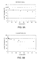
- the relationship between the volume of the main body 7 and the temperature of the LED 9 is shown in the graph (first graph) in Fig. 8A , while the relationship between the volume of the electrode portions 13a and 13b and the temperature of the LED 9 is shown in the graph (second graph) in Fig. 8B .
- the LED 9 has a junction temperature of approximately 200°C. Accordingly, it is understood that, when the main body 7 and the electrode portions 13a and 13b are designed to have the above-mentioned volumes, the thermal property data of the main body 7 and of the electrode portions 13a and 13b are equal to each other and the thermal property data are optimized.
- each of the eleven socket terminals 19a and the eleven socket terminals 19b of the socket 5 had a width of 0.2mm and these socket terminals were disposed at a distance of 0.2mm from one another.
- each of the four socket terminals 43a and the four socket terminals 43b of the socket 5a had a width of 0.91 mm and these socket terminals were disposed at a distance of 0.2mm from one another.
- a contact length in a direction perpendicular to a width direction of each socket terminal was 0.92mm.
- phosphor bronze having a thermal conductivity of 63W/mK
- copper alloy having a thermal conductivity of 264W/mK
- Other conditions were similar to those in the first example.
- a junction temperature was obtained. Results are shown in Table 2.
- Table 2 LED Junction Temperature (°C) Specification Socket 5 (11 terminals having a width of 0.2mm) Socket 5a (4 terminals having a width of 0.91 mm) Phosphor bronze (63W/mk) 164.3 132.1 Cu alloy (264W/mk) 148.8 114 Volume 2.5 4.16 Terminal/Electrode Contact Area (mm 2 ) 2.03 3.38
- the socket 5a has a lower junction temperature.
- the socket terminals having a greater width more contribute to heat dissipation or radiation.
- the main body 7 and the electrode portions 13a and 13b of the LED device 3 and the socket terminals of the socket are prevented from becoming a heat reservoir and optimized so as to contribute to heat dissipation or radiation.
- the present invention is applied to the optical semiconductor unit 1 to which the LED 9 is mounted.
- the present invention is not limited thereto but is applicable to various structures to which an optical semiconductor element emitting light is mounted.
- the present invention is also applicable to, for example, an optical semiconductor device to which a semiconductor laser is mounted.
- optical semiconductor unit of the present invention is applicable to lighting equipments in general, for example, a street light, a backlight, and a vehicle lamp.
Landscapes
- Engineering & Computer Science (AREA)
- Manufacturing & Machinery (AREA)
- Microelectronics & Electronic Packaging (AREA)
- Theoretical Computer Science (AREA)
- Computer Hardware Design (AREA)
- Physics & Mathematics (AREA)
- Evolutionary Computation (AREA)
- Geometry (AREA)
- General Engineering & Computer Science (AREA)
- General Physics & Mathematics (AREA)
- Architecture (AREA)
- Led Device Packages (AREA)
- Led Devices (AREA)
Applications Claiming Priority (1)
| Application Number | Priority Date | Filing Date | Title |
|---|---|---|---|
| JP2009058463A JP5465898B2 (ja) | 2009-03-11 | 2009-03-11 | 光半導体デバイス、ソケットおよび光半導体ユニット |
Publications (2)
| Publication Number | Publication Date |
|---|---|
| EP2228596A1 true EP2228596A1 (de) | 2010-09-15 |
| EP2228596B1 EP2228596B1 (de) | 2016-02-10 |
Family
ID=41820494
Family Applications (1)
| Application Number | Title | Priority Date | Filing Date |
|---|---|---|---|
| EP10153625.8A Not-in-force EP2228596B1 (de) | 2009-03-11 | 2010-02-15 | Optische Halbleitervorrichtung, Aufnahme und optische Halbleitereinheit |
Country Status (6)
| Country | Link |
|---|---|
| US (2) | US20100230709A1 (de) |
| EP (1) | EP2228596B1 (de) |
| JP (1) | JP5465898B2 (de) |
| KR (1) | KR101194209B1 (de) |
| CN (1) | CN101834257B (de) |
| TW (1) | TWI434461B (de) |
Cited By (3)
| Publication number | Priority date | Publication date | Assignee | Title |
|---|---|---|---|---|
| BE1019812A3 (fr) * | 2011-03-14 | 2013-01-08 | Agc Glass Europe | Panneau de vitrage comprenant une premiere feuille de verre, au moins un circuit electrique interne et un connecteur. |
| WO2013017984A1 (en) * | 2011-08-02 | 2013-02-07 | Koninklijke Philips Electronics N.V. | Modular lighting assembly adapter part |
| EP3179567A4 (de) * | 2014-08-07 | 2017-06-14 | Panasonic Intellectual Property Management Co., Ltd. | Verbinder und im verbinder verwendeter kopf und sockel |
Families Citing this family (20)
| Publication number | Priority date | Publication date | Assignee | Title |
|---|---|---|---|---|
| TW201135991A (en) * | 2010-04-12 | 2011-10-16 | Foxsemicon Integrated Tech Inc | Solid-state lighting device and light source module incorporating the same |
| USD658603S1 (en) * | 2010-06-15 | 2012-05-01 | Toshiba Lighting & Technology Corporation | Light emitting diode module |
| HK1144647A2 (en) * | 2010-10-21 | 2011-02-25 | 汪荃 | A convertible universal platform for light emitting diodes with super heat-conducting tubes |
| CN102983257A (zh) * | 2012-12-24 | 2013-03-20 | 上海顿格电子贸易有限公司 | Led灯丝接插座 |
| US8888506B2 (en) * | 2013-01-29 | 2014-11-18 | Japan Aviation Electronics Industry, Limited | Connector |
| US9565782B2 (en) * | 2013-02-15 | 2017-02-07 | Ecosense Lighting Inc. | Field replaceable power supply cartridge |
| USD777121S1 (en) * | 2013-03-05 | 2017-01-24 | Luminus Devices, Inc. | LED package |
| JP6537890B2 (ja) * | 2014-09-26 | 2019-07-03 | 日本航空電子工業株式会社 | コネクタ |
| US10477636B1 (en) | 2014-10-28 | 2019-11-12 | Ecosense Lighting Inc. | Lighting systems having multiple light sources |
| US11306897B2 (en) | 2015-02-09 | 2022-04-19 | Ecosense Lighting Inc. | Lighting systems generating partially-collimated light emissions |
| US9869450B2 (en) | 2015-02-09 | 2018-01-16 | Ecosense Lighting Inc. | Lighting systems having a truncated parabolic- or hyperbolic-conical light reflector, or a total internal reflection lens; and having another light reflector |
| US9651227B2 (en) | 2015-03-03 | 2017-05-16 | Ecosense Lighting Inc. | Low-profile lighting system having pivotable lighting enclosure |
| US9746159B1 (en) | 2015-03-03 | 2017-08-29 | Ecosense Lighting Inc. | Lighting system having a sealing system |
| US9568665B2 (en) | 2015-03-03 | 2017-02-14 | Ecosense Lighting Inc. | Lighting systems including lens modules for selectable light distribution |
| US9651216B2 (en) | 2015-03-03 | 2017-05-16 | Ecosense Lighting Inc. | Lighting systems including asymmetric lens modules for selectable light distribution |
| USD785218S1 (en) | 2015-07-06 | 2017-04-25 | Ecosense Lighting Inc. | LED luminaire having a mounting system |
| USD782093S1 (en) | 2015-07-20 | 2017-03-21 | Ecosense Lighting Inc. | LED luminaire having a mounting system |
| USD782094S1 (en) | 2015-07-20 | 2017-03-21 | Ecosense Lighting Inc. | LED luminaire having a mounting system |
| US9651232B1 (en) | 2015-08-03 | 2017-05-16 | Ecosense Lighting Inc. | Lighting system having a mounting device |
| US11639781B1 (en) | 2022-02-11 | 2023-05-02 | Toyota Motor Engineering & Manufacturing North America, Inc. | Vehicle trailer hitch illumination system |
Citations (11)
| Publication number | Priority date | Publication date | Assignee | Title |
|---|---|---|---|---|
| USRE34254E (en) * | 1989-10-05 | 1993-05-18 | Dialight Corporation | Surface mounted LED package |
| DE19751970A1 (de) * | 1996-11-26 | 1998-09-10 | Matsushita Electric Works Ltd | Flacher elektrischer Verbinder |
| JP2001024216A (ja) | 1999-07-12 | 2001-01-26 | Ichikoh Ind Ltd | 発光ダイオードの固定構造 |
| EP1429395A2 (de) * | 2002-12-09 | 2004-06-16 | Osram Sylvania Inc. | Lichtquelle, die eine Glühlampe nachahmt |
| JP2004265626A (ja) | 2003-02-13 | 2004-09-24 | Matsushita Electric Ind Co Ltd | Led光源用ソケット |
| WO2005029185A2 (en) * | 2003-09-16 | 2005-03-31 | Matsushita Electric Industrial Co., Ltd. | Led lighting source and led lighting apparatus |
| US20050276063A1 (en) * | 2004-06-10 | 2005-12-15 | Coushaine Charles M | Wedge-based lamp with LED light engine and method of making the lamp |
| US20080080187A1 (en) * | 2006-09-28 | 2008-04-03 | Purinton Richard S | Sealed LED light bulb |
| JP2008288221A (ja) | 2008-08-22 | 2008-11-27 | Koito Mfg Co Ltd | 車両用灯具 |
| US20090014732A1 (en) * | 2004-09-07 | 2009-01-15 | Takanori Nishida | Chip-type light emitting device and wiring substrate for the same |
| JP2009058463A (ja) | 2007-09-03 | 2009-03-19 | Panasonic Corp | 人体検知装置とそれを使用した衛生洗浄装置 |
Family Cites Families (23)
| Publication number | Priority date | Publication date | Assignee | Title |
|---|---|---|---|---|
| JPS5019361U (de) * | 1973-06-18 | 1975-03-04 | ||
| JPS57203573U (de) * | 1981-06-23 | 1982-12-24 | ||
| JPS58119681A (ja) * | 1982-01-09 | 1983-07-16 | Nippon Denyo Kk | ランプ |
| JPS6441153U (de) * | 1987-09-07 | 1989-03-13 | ||
| US4935856A (en) * | 1989-10-05 | 1990-06-19 | Dialight Corporation | Surface mounted LED package |
| US5923179A (en) * | 1996-03-29 | 1999-07-13 | Intel Corporation | Thermal enhancing test/burn in socket for C4 and tab packaging |
| JPH10206701A (ja) * | 1997-01-17 | 1998-08-07 | Seiko Giken:Kk | 光半導体モジュール |
| JP3504124B2 (ja) * | 1997-10-15 | 2004-03-08 | 株式会社小糸製作所 | Ledランプおよびledランプ組立体 |
| JP3356068B2 (ja) * | 1998-07-27 | 2002-12-09 | 松下電器産業株式会社 | 光電変換素子の製造方法 |
| US6386733B1 (en) * | 1998-11-17 | 2002-05-14 | Ichikoh Industries, Ltd. | Light emitting diode mounting structure |
| TW588478B (en) | 1999-09-16 | 2004-05-21 | Shinetsu Polymer Co | Method for electrically connecting two sets of electrode terminals in array on electronic board units |
| JP2003243721A (ja) * | 2002-02-18 | 2003-08-29 | Ichikoh Ind Ltd | 発光ダイオードの固定構造 |
| JP3770192B2 (ja) * | 2002-04-12 | 2006-04-26 | 松下電器産業株式会社 | チップ型led用リードフレーム |
| US7138711B2 (en) * | 2002-06-17 | 2006-11-21 | Micron Technology, Inc. | Intrinsic thermal enhancement for FBGA package |
| JP2004063973A (ja) * | 2002-07-31 | 2004-02-26 | Stanley Electric Co Ltd | 縦横マウント型電子部品 |
| JP2007018762A (ja) * | 2005-07-05 | 2007-01-25 | Sumitomo Wiring Syst Ltd | 発光装置 |
| JP2007142044A (ja) * | 2005-11-16 | 2007-06-07 | Stanley Electric Co Ltd | 半導体発光装置及びそれを用いた面光源 |
| JP2007173369A (ja) * | 2005-12-20 | 2007-07-05 | Rohm Co Ltd | 半導体発光素子及び半導体発光素子の製造方法 |
| JP4961181B2 (ja) * | 2006-09-14 | 2012-06-27 | 有限会社ブレインシステム | チップ型led用ソケット |
| TWI378580B (en) * | 2007-03-07 | 2012-12-01 | Everlight Electronics Co Ltd | Socket led device |
| JP2008288103A (ja) * | 2007-05-18 | 2008-11-27 | Smk Corp | ソケット |
| US8124988B2 (en) * | 2008-05-28 | 2012-02-28 | Semisilicon Technology Corp. | Light emitting diode lamp package structure and assembly thereof |
| US7972037B2 (en) * | 2008-11-26 | 2011-07-05 | Deloren E. Anderson | High intensity replaceable light emitting diode module and array |
-
2009
- 2009-03-11 JP JP2009058463A patent/JP5465898B2/ja not_active Expired - Fee Related
-
2010
- 2010-02-11 US US12/658,525 patent/US20100230709A1/en not_active Abandoned
- 2010-02-15 EP EP10153625.8A patent/EP2228596B1/de not_active Not-in-force
- 2010-03-03 KR KR20100018973A patent/KR101194209B1/ko not_active Expired - Fee Related
- 2010-03-03 CN CN201010129532.7A patent/CN101834257B/zh not_active Expired - Fee Related
- 2010-03-10 TW TW99106939A patent/TWI434461B/zh not_active IP Right Cessation
-
2014
- 2014-08-06 US US14/452,669 patent/US9152755B2/en not_active Expired - Fee Related
Patent Citations (11)
| Publication number | Priority date | Publication date | Assignee | Title |
|---|---|---|---|---|
| USRE34254E (en) * | 1989-10-05 | 1993-05-18 | Dialight Corporation | Surface mounted LED package |
| DE19751970A1 (de) * | 1996-11-26 | 1998-09-10 | Matsushita Electric Works Ltd | Flacher elektrischer Verbinder |
| JP2001024216A (ja) | 1999-07-12 | 2001-01-26 | Ichikoh Ind Ltd | 発光ダイオードの固定構造 |
| EP1429395A2 (de) * | 2002-12-09 | 2004-06-16 | Osram Sylvania Inc. | Lichtquelle, die eine Glühlampe nachahmt |
| JP2004265626A (ja) | 2003-02-13 | 2004-09-24 | Matsushita Electric Ind Co Ltd | Led光源用ソケット |
| WO2005029185A2 (en) * | 2003-09-16 | 2005-03-31 | Matsushita Electric Industrial Co., Ltd. | Led lighting source and led lighting apparatus |
| US20050276063A1 (en) * | 2004-06-10 | 2005-12-15 | Coushaine Charles M | Wedge-based lamp with LED light engine and method of making the lamp |
| US20090014732A1 (en) * | 2004-09-07 | 2009-01-15 | Takanori Nishida | Chip-type light emitting device and wiring substrate for the same |
| US20080080187A1 (en) * | 2006-09-28 | 2008-04-03 | Purinton Richard S | Sealed LED light bulb |
| JP2009058463A (ja) | 2007-09-03 | 2009-03-19 | Panasonic Corp | 人体検知装置とそれを使用した衛生洗浄装置 |
| JP2008288221A (ja) | 2008-08-22 | 2008-11-27 | Koito Mfg Co Ltd | 車両用灯具 |
Cited By (5)
| Publication number | Priority date | Publication date | Assignee | Title |
|---|---|---|---|---|
| BE1019812A3 (fr) * | 2011-03-14 | 2013-01-08 | Agc Glass Europe | Panneau de vitrage comprenant une premiere feuille de verre, au moins un circuit electrique interne et un connecteur. |
| WO2013017984A1 (en) * | 2011-08-02 | 2013-02-07 | Koninklijke Philips Electronics N.V. | Modular lighting assembly adapter part |
| US9587816B2 (en) | 2011-08-02 | 2017-03-07 | Philips Lighting Holding B.V. | Modular lighting assembly adapter part |
| EP3767162A1 (de) * | 2011-08-02 | 2021-01-20 | Signify Holding B.V. | Adapterteil für eine modulare beleuchtungsanordnung |
| EP3179567A4 (de) * | 2014-08-07 | 2017-06-14 | Panasonic Intellectual Property Management Co., Ltd. | Verbinder und im verbinder verwendeter kopf und sockel |
Also Published As
| Publication number | Publication date |
|---|---|
| US9152755B2 (en) | 2015-10-06 |
| EP2228596B1 (de) | 2016-02-10 |
| KR101194209B1 (ko) | 2012-10-29 |
| KR20100102536A (ko) | 2010-09-24 |
| JP2010212513A (ja) | 2010-09-24 |
| JP5465898B2 (ja) | 2014-04-09 |
| TW201044704A (en) | 2010-12-16 |
| US20140344771A1 (en) | 2014-11-20 |
| TWI434461B (zh) | 2014-04-11 |
| CN101834257A (zh) | 2010-09-15 |
| US20100230709A1 (en) | 2010-09-16 |
| CN101834257B (zh) | 2016-04-20 |
Similar Documents
| Publication | Publication Date | Title |
|---|---|---|
| EP2228596B1 (de) | Optische Halbleitervorrichtung, Aufnahme und optische Halbleitereinheit | |
| US7676915B2 (en) | Process for manufacturing an LED lamp with integrated heat sink | |
| CN102007830B (zh) | 用于将印刷电路板附着到散热器的热传导装配元件 | |
| CA2703963C (en) | Apparatus and methods for thermal management of electronic devices | |
| US10260705B2 (en) | LED lighting module with heat sink and a method of replacing an LED module | |
| US20040037044A1 (en) | Heat sink for surface mounted power devices | |
| EP2579392B1 (de) | Verbinder und beleuchtungsvorrichtung | |
| KR101134671B1 (ko) | Led 램프 모듈의 방열구조체 | |
| CN110431664B (zh) | 将led元件安装在平的载体上 | |
| US20100240158A1 (en) | Led lighting with integrated heat sink and process for manufacturing same | |
| EP1430543A2 (de) | Leuchtdiode mit integriertem kühler | |
| US7336491B2 (en) | Heat sink | |
| CN110223974B (zh) | 发光模块 | |
| JP5056327B2 (ja) | 発光装置 | |
| JP2006261221A (ja) | 電子回路及び電子機器 | |
| JP2009289841A (ja) | 発光素子収納用パッケージ | |
| KR20200133297A (ko) | 열을 효율적으로 전달할 수 있는 구조의 전극부를 구비하는 광반도체 | |
| JP2008091432A (ja) | 電子部品 | |
| JP2010034259A (ja) | 発光素子収納用パッケージ | |
| WO2003019997A1 (en) | Improved heat sink for surface mounted power devices | |
| CN121665501A (zh) | 散热件及电子装置 | |
| KR20110014274A (ko) | 발광 모듈 및 이를 갖는 발광 장치 |
Legal Events
| Date | Code | Title | Description |
|---|---|---|---|
| PUAI | Public reference made under article 153(3) epc to a published international application that has entered the european phase |
Free format text: ORIGINAL CODE: 0009012 |
|
| 17P | Request for examination filed |
Effective date: 20100215 |
|
| AK | Designated contracting states |
Kind code of ref document: A1 Designated state(s): AT BE BG CH CY CZ DE DK EE ES FI FR GB GR HR HU IE IS IT LI LT LU LV MC MK MT NL NO PL PT RO SE SI SK SM TR |
|
| AX | Request for extension of the european patent |
Extension state: AL BA RS |
|
| 17Q | First examination report despatched |
Effective date: 20110809 |
|
| GRAP | Despatch of communication of intention to grant a patent |
Free format text: ORIGINAL CODE: EPIDOSNIGR1 |
|
| INTG | Intention to grant announced |
Effective date: 20150807 |
|
| GRAS | Grant fee paid |
Free format text: ORIGINAL CODE: EPIDOSNIGR3 |
|
| GRAA | (expected) grant |
Free format text: ORIGINAL CODE: 0009210 |
|
| AK | Designated contracting states |
Kind code of ref document: B1 Designated state(s): AT BE BG CH CY CZ DE DK EE ES FI FR GB GR HR HU IE IS IT LI LT LU LV MC MK MT NL NO PL PT RO SE SI SK SM TR |
|
| REG | Reference to a national code |
Ref country code: GB Ref legal event code: FG4D |
|
| REG | Reference to a national code |
Ref country code: AT Ref legal event code: REF Ref document number: 774834 Country of ref document: AT Kind code of ref document: T Effective date: 20160215 Ref country code: CH Ref legal event code: EP |
|
| REG | Reference to a national code |
Ref country code: IE Ref legal event code: FG4D |
|
| REG | Reference to a national code |
Ref country code: DE Ref legal event code: R096 Ref document number: 602010030500 Country of ref document: DE |
|
| REG | Reference to a national code |
Ref country code: NL Ref legal event code: FP |
|
| REG | Reference to a national code |
Ref country code: LT Ref legal event code: MG4D |
|
| REG | Reference to a national code |
Ref country code: AT Ref legal event code: MK05 Ref document number: 774834 Country of ref document: AT Kind code of ref document: T Effective date: 20160210 |
|
| PG25 | Lapsed in a contracting state [announced via postgrant information from national office to epo] |
Ref country code: HR Free format text: LAPSE BECAUSE OF FAILURE TO SUBMIT A TRANSLATION OF THE DESCRIPTION OR TO PAY THE FEE WITHIN THE PRESCRIBED TIME-LIMIT Effective date: 20160210 Ref country code: ES Free format text: LAPSE BECAUSE OF FAILURE TO SUBMIT A TRANSLATION OF THE DESCRIPTION OR TO PAY THE FEE WITHIN THE PRESCRIBED TIME-LIMIT Effective date: 20160210 Ref country code: NO Free format text: LAPSE BECAUSE OF FAILURE TO SUBMIT A TRANSLATION OF THE DESCRIPTION OR TO PAY THE FEE WITHIN THE PRESCRIBED TIME-LIMIT Effective date: 20160510 Ref country code: FI Free format text: LAPSE BECAUSE OF FAILURE TO SUBMIT A TRANSLATION OF THE DESCRIPTION OR TO PAY THE FEE WITHIN THE PRESCRIBED TIME-LIMIT Effective date: 20160210 Ref country code: IT Free format text: LAPSE BECAUSE OF FAILURE TO SUBMIT A TRANSLATION OF THE DESCRIPTION OR TO PAY THE FEE WITHIN THE PRESCRIBED TIME-LIMIT Effective date: 20160210 Ref country code: GR Free format text: LAPSE BECAUSE OF FAILURE TO SUBMIT A TRANSLATION OF THE DESCRIPTION OR TO PAY THE FEE WITHIN THE PRESCRIBED TIME-LIMIT Effective date: 20160511 |
|
| PG25 | Lapsed in a contracting state [announced via postgrant information from national office to epo] |
Ref country code: PT Free format text: LAPSE BECAUSE OF FAILURE TO SUBMIT A TRANSLATION OF THE DESCRIPTION OR TO PAY THE FEE WITHIN THE PRESCRIBED TIME-LIMIT Effective date: 20160613 Ref country code: IS Free format text: LAPSE BECAUSE OF FAILURE TO SUBMIT A TRANSLATION OF THE DESCRIPTION OR TO PAY THE FEE WITHIN THE PRESCRIBED TIME-LIMIT Effective date: 20160610 Ref country code: PL Free format text: LAPSE BECAUSE OF FAILURE TO SUBMIT A TRANSLATION OF THE DESCRIPTION OR TO PAY THE FEE WITHIN THE PRESCRIBED TIME-LIMIT Effective date: 20160210 Ref country code: LV Free format text: LAPSE BECAUSE OF FAILURE TO SUBMIT A TRANSLATION OF THE DESCRIPTION OR TO PAY THE FEE WITHIN THE PRESCRIBED TIME-LIMIT Effective date: 20160210 Ref country code: LT Free format text: LAPSE BECAUSE OF FAILURE TO SUBMIT A TRANSLATION OF THE DESCRIPTION OR TO PAY THE FEE WITHIN THE PRESCRIBED TIME-LIMIT Effective date: 20160210 Ref country code: BE Free format text: LAPSE BECAUSE OF NON-PAYMENT OF DUE FEES Effective date: 20160229 Ref country code: AT Free format text: LAPSE BECAUSE OF FAILURE TO SUBMIT A TRANSLATION OF THE DESCRIPTION OR TO PAY THE FEE WITHIN THE PRESCRIBED TIME-LIMIT Effective date: 20160210 Ref country code: SE Free format text: LAPSE BECAUSE OF FAILURE TO SUBMIT A TRANSLATION OF THE DESCRIPTION OR TO PAY THE FEE WITHIN THE PRESCRIBED TIME-LIMIT Effective date: 20160210 |
|
| REG | Reference to a national code |
Ref country code: CH Ref legal event code: PL |
|
| PG25 | Lapsed in a contracting state [announced via postgrant information from national office to epo] |
Ref country code: LI Free format text: LAPSE BECAUSE OF NON-PAYMENT OF DUE FEES Effective date: 20160229 Ref country code: DK Free format text: LAPSE BECAUSE OF FAILURE TO SUBMIT A TRANSLATION OF THE DESCRIPTION OR TO PAY THE FEE WITHIN THE PRESCRIBED TIME-LIMIT Effective date: 20160210 Ref country code: CH Free format text: LAPSE BECAUSE OF NON-PAYMENT OF DUE FEES Effective date: 20160229 Ref country code: EE Free format text: LAPSE BECAUSE OF FAILURE TO SUBMIT A TRANSLATION OF THE DESCRIPTION OR TO PAY THE FEE WITHIN THE PRESCRIBED TIME-LIMIT Effective date: 20160210 |
|
| REG | Reference to a national code |
Ref country code: DE Ref legal event code: R097 Ref document number: 602010030500 Country of ref document: DE |
|
| PG25 | Lapsed in a contracting state [announced via postgrant information from national office to epo] |
Ref country code: CZ Free format text: LAPSE BECAUSE OF FAILURE TO SUBMIT A TRANSLATION OF THE DESCRIPTION OR TO PAY THE FEE WITHIN THE PRESCRIBED TIME-LIMIT Effective date: 20160210 Ref country code: RO Free format text: LAPSE BECAUSE OF FAILURE TO SUBMIT A TRANSLATION OF THE DESCRIPTION OR TO PAY THE FEE WITHIN THE PRESCRIBED TIME-LIMIT Effective date: 20160210 Ref country code: SM Free format text: LAPSE BECAUSE OF FAILURE TO SUBMIT A TRANSLATION OF THE DESCRIPTION OR TO PAY THE FEE WITHIN THE PRESCRIBED TIME-LIMIT Effective date: 20160210 Ref country code: SK Free format text: LAPSE BECAUSE OF FAILURE TO SUBMIT A TRANSLATION OF THE DESCRIPTION OR TO PAY THE FEE WITHIN THE PRESCRIBED TIME-LIMIT Effective date: 20160210 |
|
| REG | Reference to a national code |
Ref country code: IE Ref legal event code: MM4A |
|
| PLBE | No opposition filed within time limit |
Free format text: ORIGINAL CODE: 0009261 |
|
| STAA | Information on the status of an ep patent application or granted ep patent |
Free format text: STATUS: NO OPPOSITION FILED WITHIN TIME LIMIT |
|
| PG25 | Lapsed in a contracting state [announced via postgrant information from national office to epo] |
Ref country code: BE Free format text: LAPSE BECAUSE OF FAILURE TO SUBMIT A TRANSLATION OF THE DESCRIPTION OR TO PAY THE FEE WITHIN THE PRESCRIBED TIME-LIMIT Effective date: 20160210 |
|
| 26N | No opposition filed |
Effective date: 20161111 |
|
| GBPC | Gb: european patent ceased through non-payment of renewal fee |
Effective date: 20160510 |
|
| PG25 | Lapsed in a contracting state [announced via postgrant information from national office to epo] |
Ref country code: IE Free format text: LAPSE BECAUSE OF NON-PAYMENT OF DUE FEES Effective date: 20160215 |
|
| REG | Reference to a national code |
Ref country code: FR Ref legal event code: ST Effective date: 20170102 |
|
| PG25 | Lapsed in a contracting state [announced via postgrant information from national office to epo] |
Ref country code: BG Free format text: LAPSE BECAUSE OF FAILURE TO SUBMIT A TRANSLATION OF THE DESCRIPTION OR TO PAY THE FEE WITHIN THE PRESCRIBED TIME-LIMIT Effective date: 20160510 Ref country code: SI Free format text: LAPSE BECAUSE OF FAILURE TO SUBMIT A TRANSLATION OF THE DESCRIPTION OR TO PAY THE FEE WITHIN THE PRESCRIBED TIME-LIMIT Effective date: 20160210 |
|
| PGFP | Annual fee paid to national office [announced via postgrant information from national office to epo] |
Ref country code: NL Payment date: 20170110 Year of fee payment: 8 |
|
| PG25 | Lapsed in a contracting state [announced via postgrant information from national office to epo] |
Ref country code: FR Free format text: LAPSE BECAUSE OF NON-PAYMENT OF DUE FEES Effective date: 20160411 |
|
| PG25 | Lapsed in a contracting state [announced via postgrant information from national office to epo] |
Ref country code: GB Free format text: LAPSE BECAUSE OF NON-PAYMENT OF DUE FEES Effective date: 20160510 |
|
| PG25 | Lapsed in a contracting state [announced via postgrant information from national office to epo] |
Ref country code: MT Free format text: LAPSE BECAUSE OF FAILURE TO SUBMIT A TRANSLATION OF THE DESCRIPTION OR TO PAY THE FEE WITHIN THE PRESCRIBED TIME-LIMIT Effective date: 20160210 |
|
| PG25 | Lapsed in a contracting state [announced via postgrant information from national office to epo] |
Ref country code: CY Free format text: LAPSE BECAUSE OF FAILURE TO SUBMIT A TRANSLATION OF THE DESCRIPTION OR TO PAY THE FEE WITHIN THE PRESCRIBED TIME-LIMIT Effective date: 20160210 Ref country code: HU Free format text: LAPSE BECAUSE OF FAILURE TO SUBMIT A TRANSLATION OF THE DESCRIPTION OR TO PAY THE FEE WITHIN THE PRESCRIBED TIME-LIMIT; INVALID AB INITIO Effective date: 20100215 |
|
| PG25 | Lapsed in a contracting state [announced via postgrant information from national office to epo] |
Ref country code: MK Free format text: LAPSE BECAUSE OF FAILURE TO SUBMIT A TRANSLATION OF THE DESCRIPTION OR TO PAY THE FEE WITHIN THE PRESCRIBED TIME-LIMIT Effective date: 20160210 Ref country code: LU Free format text: LAPSE BECAUSE OF NON-PAYMENT OF DUE FEES Effective date: 20160215 Ref country code: TR Free format text: LAPSE BECAUSE OF FAILURE TO SUBMIT A TRANSLATION OF THE DESCRIPTION OR TO PAY THE FEE WITHIN THE PRESCRIBED TIME-LIMIT Effective date: 20160210 Ref country code: MT Free format text: LAPSE BECAUSE OF FAILURE TO SUBMIT A TRANSLATION OF THE DESCRIPTION OR TO PAY THE FEE WITHIN THE PRESCRIBED TIME-LIMIT Effective date: 20160229 Ref country code: MC Free format text: LAPSE BECAUSE OF FAILURE TO SUBMIT A TRANSLATION OF THE DESCRIPTION OR TO PAY THE FEE WITHIN THE PRESCRIBED TIME-LIMIT Effective date: 20160210 |
|
| REG | Reference to a national code |
Ref country code: NL Ref legal event code: MM Effective date: 20180301 |
|
| PG25 | Lapsed in a contracting state [announced via postgrant information from national office to epo] |
Ref country code: NL Free format text: LAPSE BECAUSE OF NON-PAYMENT OF DUE FEES Effective date: 20180301 |
|
| PGFP | Annual fee paid to national office [announced via postgrant information from national office to epo] |
Ref country code: DE Payment date: 20190205 Year of fee payment: 10 |
|
| REG | Reference to a national code |
Ref country code: DE Ref legal event code: R119 Ref document number: 602010030500 Country of ref document: DE |
|
| PG25 | Lapsed in a contracting state [announced via postgrant information from national office to epo] |
Ref country code: DE Free format text: LAPSE BECAUSE OF NON-PAYMENT OF DUE FEES Effective date: 20200901 |