EP2221900A2 - Organisches EL-Modul - Google Patents
Organisches EL-Modul Download PDFInfo
- Publication number
- EP2221900A2 EP2221900A2 EP10153167A EP10153167A EP2221900A2 EP 2221900 A2 EP2221900 A2 EP 2221900A2 EP 10153167 A EP10153167 A EP 10153167A EP 10153167 A EP10153167 A EP 10153167A EP 2221900 A2 EP2221900 A2 EP 2221900A2
- Authority
- EP
- European Patent Office
- Prior art keywords
- organic
- element substrate
- anode
- substrate
- cathode
- Prior art date
- Legal status (The legal status is an assumption and is not a legal conclusion. Google has not performed a legal analysis and makes no representation as to the accuracy of the status listed.)
- Withdrawn
Links
- 238000005401 electroluminescence Methods 0.000 claims abstract description 69
- 239000000758 substrate Substances 0.000 claims abstract description 64
- 239000004020 conductor Substances 0.000 claims abstract description 17
- 238000005452 bending Methods 0.000 claims abstract description 9
- 238000007789 sealing Methods 0.000 claims description 24
- 239000012044 organic layer Substances 0.000 claims description 14
- 230000002093 peripheral effect Effects 0.000 claims description 5
- 239000010410 layer Substances 0.000 description 9
- CNQCVBJFEGMYDW-UHFFFAOYSA-N lawrencium atom Chemical compound [Lr] CNQCVBJFEGMYDW-UHFFFAOYSA-N 0.000 description 6
- 238000004519 manufacturing process Methods 0.000 description 4
- 229920001971 elastomer Polymers 0.000 description 3
- 239000000806 elastomer Substances 0.000 description 3
- 239000000463 material Substances 0.000 description 3
- 239000011347 resin Substances 0.000 description 3
- 229920005989 resin Polymers 0.000 description 3
- 238000004070 electrodeposition Methods 0.000 description 2
- 229910052751 metal Inorganic materials 0.000 description 2
- 239000002184 metal Substances 0.000 description 2
- 238000012986 modification Methods 0.000 description 2
- 230000004048 modification Effects 0.000 description 2
- 229920001296 polysiloxane Polymers 0.000 description 2
- TVIVIEFSHFOWTE-UHFFFAOYSA-K tri(quinolin-8-yloxy)alumane Chemical compound [Al+3].C1=CN=C2C([O-])=CC=CC2=C1.C1=CN=C2C([O-])=CC=CC2=C1.C1=CN=C2C([O-])=CC=CC2=C1 TVIVIEFSHFOWTE-UHFFFAOYSA-K 0.000 description 2
- 239000004593 Epoxy Substances 0.000 description 1
- WHXSMMKQMYFTQS-UHFFFAOYSA-N Lithium Chemical compound [Li] WHXSMMKQMYFTQS-UHFFFAOYSA-N 0.000 description 1
- -1 acryl Chemical group 0.000 description 1
- 229910052782 aluminium Inorganic materials 0.000 description 1
- XAGFODPZIPBFFR-UHFFFAOYSA-N aluminium Chemical compound [Al] XAGFODPZIPBFFR-UHFFFAOYSA-N 0.000 description 1
- 150000004982 aromatic amines Chemical class 0.000 description 1
- QVGXLLKOCUKJST-UHFFFAOYSA-N atomic oxygen Chemical compound [O] QVGXLLKOCUKJST-UHFFFAOYSA-N 0.000 description 1
- 239000011248 coating agent Substances 0.000 description 1
- 238000000576 coating method Methods 0.000 description 1
- 230000000694 effects Effects 0.000 description 1
- 239000005357 flat glass Substances 0.000 description 1
- 239000011521 glass Substances 0.000 description 1
- 230000005525 hole transport Effects 0.000 description 1
- AMGQUBHHOARCQH-UHFFFAOYSA-N indium;oxotin Chemical compound [In].[Sn]=O AMGQUBHHOARCQH-UHFFFAOYSA-N 0.000 description 1
- 238000002347 injection Methods 0.000 description 1
- 239000007924 injection Substances 0.000 description 1
- 238000007641 inkjet printing Methods 0.000 description 1
- 238000010030 laminating Methods 0.000 description 1
- 229910052744 lithium Inorganic materials 0.000 description 1
- 150000002739 metals Chemical class 0.000 description 1
- 238000000034 method Methods 0.000 description 1
- 229910052760 oxygen Inorganic materials 0.000 description 1
- 239000001301 oxygen Substances 0.000 description 1
- 230000000149 penetrating effect Effects 0.000 description 1
- 230000001681 protective effect Effects 0.000 description 1
- 229920002379 silicone rubber Polymers 0.000 description 1
- 239000004945 silicone rubber Substances 0.000 description 1
- 239000000126 substance Substances 0.000 description 1
- 238000001771 vacuum deposition Methods 0.000 description 1
Images

Classifications
-
- H—ELECTRICITY
- H10—SEMICONDUCTOR DEVICES; ELECTRIC SOLID-STATE DEVICES NOT OTHERWISE PROVIDED FOR
- H10K—ORGANIC ELECTRIC SOLID-STATE DEVICES
- H10K50/00—Organic light-emitting devices
- H10K50/80—Constructional details
- H10K50/805—Electrodes
-
- H—ELECTRICITY
- H05—ELECTRIC TECHNIQUES NOT OTHERWISE PROVIDED FOR
- H05K—PRINTED CIRCUITS; CASINGS OR CONSTRUCTIONAL DETAILS OF ELECTRIC APPARATUS; MANUFACTURE OF ASSEMBLAGES OF ELECTRICAL COMPONENTS
- H05K1/00—Printed circuits
- H05K1/02—Details
- H05K1/0277—Bendability or stretchability details
- H05K1/028—Bending or folding regions of flexible printed circuits
-
- H—ELECTRICITY
- H05—ELECTRIC TECHNIQUES NOT OTHERWISE PROVIDED FOR
- H05K—PRINTED CIRCUITS; CASINGS OR CONSTRUCTIONAL DETAILS OF ELECTRIC APPARATUS; MANUFACTURE OF ASSEMBLAGES OF ELECTRICAL COMPONENTS
- H05K1/00—Printed circuits
- H05K1/02—Details
- H05K1/14—Structural association of two or more printed circuits
- H05K1/147—Structural association of two or more printed circuits at least one of the printed circuits being bent or folded, e.g. by using a flexible printed circuit
-
- H—ELECTRICITY
- H05—ELECTRIC TECHNIQUES NOT OTHERWISE PROVIDED FOR
- H05K—PRINTED CIRCUITS; CASINGS OR CONSTRUCTIONAL DETAILS OF ELECTRIC APPARATUS; MANUFACTURE OF ASSEMBLAGES OF ELECTRICAL COMPONENTS
- H05K1/00—Printed circuits
- H05K1/18—Printed circuits structurally associated with non-printed electric components
- H05K1/189—Printed circuits structurally associated with non-printed electric components characterised by the use of a flexible or folded printed circuit
-
- H—ELECTRICITY
- H05—ELECTRIC TECHNIQUES NOT OTHERWISE PROVIDED FOR
- H05K—PRINTED CIRCUITS; CASINGS OR CONSTRUCTIONAL DETAILS OF ELECTRIC APPARATUS; MANUFACTURE OF ASSEMBLAGES OF ELECTRICAL COMPONENTS
- H05K2201/00—Indexing scheme relating to printed circuits covered by H05K1/00
- H05K2201/05—Flexible printed circuits [FPCs]
- H05K2201/055—Folded back on itself
-
- H—ELECTRICITY
- H05—ELECTRIC TECHNIQUES NOT OTHERWISE PROVIDED FOR
- H05K—PRINTED CIRCUITS; CASINGS OR CONSTRUCTIONAL DETAILS OF ELECTRIC APPARATUS; MANUFACTURE OF ASSEMBLAGES OF ELECTRICAL COMPONENTS
- H05K2201/00—Indexing scheme relating to printed circuits covered by H05K1/00
- H05K2201/10—Details of components or other objects attached to or integrated in a printed circuit board
- H05K2201/10007—Types of components
- H05K2201/10128—Display
Definitions
- the present invention generally relates to an organic electroluminescence (EL) module, capable of emitting light through organic EL.
- EL organic electroluminescence
- FIG. 11 shows the organic EL module.
- the organic EL module 100 includes a quadrangular element substrate 102 formed by glass, an organic EL element 103 formed by laminating anodes 131P, an organic layer, and cathodes 131M in sequence, a sealing portion 104 formed by silicone and for sealing the organic EL element 103, and wiring boards 105P and 105M for respectively supplying power to the anodes 131P and the cathodes 131M.
- An area of the organic EL element 103 is smaller than that of the element substrate 102, and the organic EL element 103 is formed near a center of the element substrate 102.
- the organic EL element 103 supplies the power to the anodes 131P and the cathodes 131M from a plurality of surrounding directions. Therefore, a part of the anodes 131P and a part of the cathodes 131M extend from the sealing portion 104 to the outside differently, and are formed on the element substrate 102 along a plurality of outer peripheral edges of the element substrate 102.
- the wiring boards 105P and 105M are in a U shape having corners, are arranged on an outer periphery of the element substrate 102, and are respectively connected to the plurality of anodes 131P and cathodes 131 M.
- the wiring boards 105P and 105M are connected to a direct current (DC) power source outside the organic EL module 100, and supply the power to the anodes 131P and the cathodes 131M.
- DC direct current
- the wiring boards 105P and 105M for supplying the power are in a U shape having corners, an L shape, or a frame shape, and are arranged in a manner of surrounding the organic EL element 103.
- the wiring boards 105P and 105M form the U shape having the corners or the like by cutting a rectangular conductive plate serving as a base material. Therefore, the part of the base material surrounded by the U shape having the corners becomes useless, a processing loss of the wiring boards 105P and 104M is relatively high, and a manufacturing cost becomes high.
- the present invention is used to solve the problems, such that in an organic EL module, a processing loss of wiring boards for supplying power to an anode and a cathode is reduced, so as to lower a manufacturing cost.
- one aspect of the present invention is to provide an organic EL module, which includes a polygonal element substrate, having a light transmissive property; an organic EL element, including electrodes and an organic layer, in which the electrodes are formed by an anode and a cathode laminated on the element substrate; a sealing portion, arranged opposite to the element substrate, for sealing the organic EL element; and at least one pair of wiring boards, for supplying power to the anode and the cathode of the organic EL element.
- the organic EL element and the sealing portion are formed in a region inside an outer periphery of the element substrate, and parts of the anode and parts of the cathode extend to outside of an outer periphery of the sealing portion differently, and are formed on the element substrate along a plurality of outer peripheral edges of the element substrate.
- Each wiring board is formed by bending a strip conductor in a manner that parts of the strip in the same surface contacting each other, and is arranged on the outer periphery of the element substrate in a manner of connecting the anode in the extended parts with a same pole and connecting the cathode in the extended parts with a same pole.
- the wiring boards are lead frames, and parts of the wiring boards contacting with the electrodes are in a wave shape.
- the wiring board is a flexible wiring substrate comprising a flexible substrate and flat conductors disposed on two sides of the flexible substrate.
- the wiring boards are formed by the bent strip conductor, such that the wiring boards having a width satisfying a shape of the electrodes without cutting a conductive plate into a U shape, and the processing loss is reduced, thereby lowering the manufacturing cost.
- the wiring boards contact the electrodes through a plurality of contacting portions, such that the wiring boards surely contact the electrodes even if the electrodes have high resistance, so as to uniformly supply the power to the electrodes, thereby obtaining a uniform light emitting surface.
- the wiring board is a flexible wiring substrate, and is bent to press and contact the electrodes, such that when the flexible wiring substrate is used to press and contact a plurality of electrodes, it is easier to absorb the size deviation of the flexible substrate, contact position deviation, and electrode position deviation.
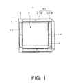
- FIG. 1 is a plan view of an organic EL module according to a first embodiment of the present invention.
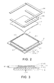
- FIG. 2 is a three-dimensional exploded view of the organic EL module.
- FIG. 3 is a cross-sectional view of an organic EL element in the organic EL module.
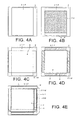
- FIGs. 4A to 4E are plan views showing the sequence of forming the organic EL module.
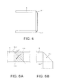
- FIG. 5 is a plan view of a wiring board in the organic EL module.
- FIG. 6A is a partial enlarged view of the wiring board before being bent
- FIG. 6B is a partial enlarged view of the wiring board after being bent.
- FIG. 7 is a plan perspective view of an organic EL module according to a variation of this embodiment.
- FIG. 8 is an end view drawing along line A-A of FIG. 7 .
- FIG. 9 is an end view drawing of a case of the organic EL module along line B-B of FIG. 7 .
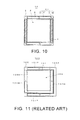
- FIG. 10 is a plan view of an organic EL module according to a second embodiment of the present invention.
- FIG. 11 is a plan view of a conventional organic EL module.
- the organic EL module 1 includes a polygonal element substrate 2, having a light transmissive property; an organic EL element 3, including electrodes 31 and an organic layer 32, in which the electrodes 31 are formed by an anode 31P and a cathodes 31M laminated on the element substrate 2; a sealing portion 4, arranged opposite to the element substrate 2, for sealing the organic EL element 3; a wiring board 5P, for supplying power to the anode 31P; and a wiring board 5M, for supplying power to the cathodes 31 M.
- the organic EL element 3 and the sealing portion 4 are formed in a region inside an outer periphery of the element substrate 2. Parts of the anode 31P and parts of the cathode 31M extend to outside of an outer periphery of the sealing portion 4 differently, and are formed on the element substrate 2 along a plurality of outer peripheral edges 21 of the element substrate 2.
- Each wiring board 5P and 5M is formed by bending a strip conductor in a manner that parts of the strip in the same surface contacting each other.
- the wiring board 5P is arranged on the outer periphery of the element substrate 2 in a manner of connecting the extended anode 31P
- the wiring board 5M is arranged on the outer periphery of the element substrate 2 in a manner of connecting the extended cathode 31M.
- the wiring boards 5P and 5M are respectively connected to a positive pole and a negative pole of a DC power source disposed outside the organic EL module 1 through a pair of conducting wires.
- the wiring boards 5P and 5M have the same potential, such that the conducting wires are installed at appropriate positions of the wiring boards 5P and 5M.
- the organic EL element 3 is a surface light emitting source, and is formed on the element substrate 2 formed by flat glass or acryl resin etc.
- Layers of the organic EL element 3 include the anode 31P serving as the transparent electrode, the organic layer 32, and the cathode 31M, which are laminated in sequence through a vacuum evaporation method or an ink jetting method.
- the material of each layer is as follows: for example, the anode 31P is made of indium tin oxide (ITO), the organic layer 32 is made of Alq 3 , and the cathode 31M is made of aluminum or other metals.
- ITO indium tin oxide
- the organic layer 32 is made of Alq 3
- the cathode 31M is made of aluminum or other metals.
- the wiring boards supply the power to the anode 31P and the cathode 31M from the DC power source 6, such that light is emitted from the organic layer 32.
- the light emitted from the organic layer 32 exits to the outside after passing through the transparent anode 31P and the element substrate 2.
- the cathode 31 formed by the metal reflects the light incident from the organic layer 32 to the element substrate 2.
- other layers may be further laminated on the organic layer 32, for example, a hole transport layer formed by arylamine may be laminated on the anode 31P side of the light emitting layer, or an electron injection layer formed by lithium complex is laminated on the cathode 31M side.
- the sequence of forming the organic EL module 1 is described. As shown in FIG. 4A , firstly, the anode 31P is laminated on the element substrate 2.
- the organic layer 32 (dot pattern portion) is laminated on the anode 31P.
- the organic layer 32 is formed adjacent to a central portion of the element substrate 2, that is, the organic layer 32 is formed in the region inside the outer periphery of the element substrate 2.
- the cathode 31M is laminated.
- the organic layer 32 is sandwiched between the anode 31P and the cathode 31M, so as to form the organic EL element 3.
- the sealing portion 4 is formed by coating silicone, epoxy, or other sealing resins.
- the sealing portion 4 wraps the organic EL element 3, so as to protect the organic EL element 3 from being affected by moisture or oxygen in the air.
- Parts of the anode 31P extend to the outside of the outer periphery of the sealing portion 4 (a vertical direction in the drawing), a group of opposite edges of the anode 31P are located on the outside of the outer periphery of the sealing portion 4, and other opposite edges are located on a region inside the outer periphery of the sealing portion 4.
- Parts of the cathode 31M extend to the outside of the outer periphery of the sealing portion 4 (a horizontal direction in the drawing) in a direction approximately orthogonal to an extending direction of the anode 31P.
- the extended parts of the anode 31P and the cathode 31M are exposed out of the sealing portion 4.
- the electrodes with the same pole are arranged on the opposite edges of the element substrate 2.
- the wiring boards 5P and 5M in a U shape having corners are arranged in a manner of not overlapping with each other on the outer periphery of the element substrate 2.
- the wiring board 5P of a positive side contacts two extended parts of the anode 31P
- the wiring board 5M on a negative side contacts the two extended parts of the cathode 31 M.
- the wiring boards 5P and 5M need not to be entirely located on the outer periphery of the element substrate 2, that is, a part may be disposed on the sealing portion 4, or extends out of the element substrate 2.
- the wiring board 5 is formed by approximately perpendicularly bending a strip conductor formed by a lead frame at bending portions 51, such that the wiring board 5 forms, for example, the U shape having corners. Further, under the installed state, the wiring board 5 is in a shape enabling the electrodes with the same pole among the plurality of electrodes 31, which are oppositely exposed on the element substrate 2, connected to each other.
- the wiring board 5 is valley-folded at a score 52 approximately at an angle of 45° with a longitudinal direction, and is bent in a manner of contacting surfaces 53 and 54 adjacent to two sides of the score 52, so as to form the bending portion 51 bent perpendicularly, as shown in FIG. 6B .
- the wiring board 5 is formed by the bent strip conductor, such that the wiring board 5 may realize a shape having a width satisfying a shape of the electrodes 31 without cutting a conductive plate into a U shape, and the processing loss is reduced, thereby lowering the manufacturing cost.
- an organic EL module according to the variation of the first embodiment is described.
- the organic EL module 11 of this variation is accommodated in a case 7.
- wiring boards 5 are lead frames, and parts of the wiring boards 5 contacting electrodes 31 are in a wave shape.
- the wiring boards 5 include a wiring board 5P of a positive side and a wiring board 5M of a negative side disposed in pair, and parts of the wiring board 5P and the wiring board 5M contacting the anode 31P and the cathode 31M respectively form the wave shape.
- only the wiring board 5P of the positive side in the wiring boards 5 is in the wave shape, and the wiring board 5M of the negative side is in a flat shape.
- the case 7 is made by resin processed into a case shape, and is formed by a front case 71 and a back case 72.
- an element substrate 2 emitting the light serves as the front case 71 to accommodate the organic EL module 11, and the front case 71 and the back case 72 are engaged.
- a thermally conductive elastomer 8 formed by silicone rubber or the like is disposed between the parts of the wiring boards 5 forming the wave shape and the back case 72.
- the thermally conductive elastomer 8 presses the wiring board 5 on the electrodes 31 to form an electrical connection.
- the wiring boards 5 are connected to a DC power source outside the case 7 through conducting wires penetrating the back case 72.
- the organic EL element 3 supplies power to the electrodes 31 through the wiring boards 5, so as to emit the light. Heat generated by the organic EL element 3 is delivered to the back case 72 through the thermally conductive elastomer 8, and is released to the atmosphere from the back case 72.
- an opening portion 73 is disposed on a part of the front case 71 opposite to the organic EL element 3. The light emitted from the organic EL element 3 is irradiated through the opening portion 73.
- the wiring boards 5 contact the electrodes 31 through a plurality of contacting portions, such that the wiring boards 5 surely contact the electrodes 31 even if the electrodes 31 have relatively high resistance, so as to uniformly supply the power to the electrodes 31, thereby obtaining a uniform light emitting surface.
- the wiring board 5 is a flexible wiring substrate having flat conductors on two sides of a flexible substrate, so as to replace the single-plate conductor of the first embodiment.
- the flexible wiring substrate includes an insulating substrate serving as a base plate; conductors on two sides of the substrate, and cover layers (surface protective films) on surfaces of the conductors.
- the wiring board 5 is formed by bending the flexible wiring substrate in a strip shape in a manner that parts of the strip on the same surface contacting each other, so as to form a frame shape of surrounding the organic EL element 3.
- ACF anisotropic conducting film
- the wiring board 5 being the flexible wiring substrate is bent to press and contact the electrodes 31, such that when a flexible wiring substrate is used to press and contact a plurality of electrodes 31, it is easier to absorb the size deviation of the flexible substrate, contact position deviation, and electrode position deviation.
- the wiring boards may be bent to form an L shape, and a pair of L-shaped wiring boards is arranged on the element substrate in a manner that the bending portions of the wiring boards are located on diagonal corners.
- the organic EL element may also be hexagonal, and the anode and the cathode differently extend towards three directions respectively, such that the anode and the cathode are connected to the flexile wiring substrate bent to an angle of approximately 120°.
Applications Claiming Priority (1)
| Application Number | Priority Date | Filing Date | Title |
|---|---|---|---|
| JP2009038008A JP5240718B2 (ja) | 2009-02-20 | 2009-02-20 | 有機elモジュール |
Publications (2)
| Publication Number | Publication Date |
|---|---|
| EP2221900A2 true EP2221900A2 (de) | 2010-08-25 |
| EP2221900A3 EP2221900A3 (de) | 2013-09-04 |
Family
ID=42102157
Family Applications (1)
| Application Number | Title | Priority Date | Filing Date |
|---|---|---|---|
| EP10153167.1A Withdrawn EP2221900A3 (de) | 2009-02-20 | 2010-02-10 | Organisches EL-Modul |
Country Status (4)
| Country | Link |
|---|---|
| US (1) | US8207664B2 (de) |
| EP (1) | EP2221900A3 (de) |
| JP (1) | JP5240718B2 (de) |
| CN (1) | CN101814584B (de) |
Cited By (4)
| Publication number | Priority date | Publication date | Assignee | Title |
|---|---|---|---|---|
| WO2013124766A1 (en) * | 2012-02-21 | 2013-08-29 | Koninklijke Philips N.V. | Luminaire element |
| WO2013150003A1 (de) * | 2012-04-05 | 2013-10-10 | Ledon Oled Lighting Gmbh & Co. Kg | Lichtabgabevorrichtung mit einem oled-element |
| EP2763502A4 (de) * | 2011-09-30 | 2015-12-30 | Idemitsu Kosan Co | Planare lichtemittierende vorrichtung |
| EP3010062A4 (de) * | 2013-07-24 | 2017-03-08 | LG Display Co., Ltd. | Flexible leiterplattenstruktur |
Families Citing this family (14)
| Publication number | Priority date | Publication date | Assignee | Title |
|---|---|---|---|---|
| CN102860128A (zh) * | 2010-04-27 | 2013-01-02 | 日商路米欧技术股份有限公司 | 有机el照明装置 |
| CN104136833B (zh) * | 2012-02-21 | 2017-04-12 | 飞利浦照明控股有限公司 | 灯具元件 |
| KR101879831B1 (ko) * | 2012-03-21 | 2018-07-20 | 삼성디스플레이 주식회사 | 플렉시블 표시 장치, 유기 발광 표시 장치 및 플렉시블 표시 장치용 원장 기판 |
| CN104012174A (zh) | 2012-07-06 | 2014-08-27 | 株式会社钟化 | 有机el模块以及有机el模块的供电构造 |
| KR101514114B1 (ko) * | 2012-09-14 | 2015-04-21 | 주식회사 엘지화학 | Oled 조명 모듈 |
| KR101588499B1 (ko) | 2013-07-24 | 2016-01-25 | 주식회사 엘지화학 | 연성인쇄회로기판의 구조체 |
| US10084135B2 (en) | 2014-11-27 | 2018-09-25 | Industrial Technology Research Institute | Illumination device and method of fabricating an illumination device |
| JP2016181412A (ja) * | 2015-03-24 | 2016-10-13 | デクセリアルズ株式会社 | 有機el照明パネル及びその製造方法 |
| WO2016170621A1 (ja) * | 2015-04-22 | 2016-10-27 | 堺ディスプレイプロダクト株式会社 | 光源装置、表示装置、基板ユニットの製造方法及び光源装置の製造方法 |
| WO2017006392A1 (ja) * | 2015-07-03 | 2017-01-12 | パイオニア株式会社 | 発光装置 |
| WO2017033630A1 (ja) * | 2015-08-26 | 2017-03-02 | 株式会社カネカ | 面状発光装置 |
| US10381587B2 (en) * | 2016-03-02 | 2019-08-13 | Konica Minolta, Inc. | Light emitting apparatus containing sealing member to cover planar light emitter |
| US10991910B2 (en) * | 2017-03-30 | 2021-04-27 | Sharp Kabushiki Kaisha | Display device and production method therefor |
| WO2024069612A1 (en) * | 2022-09-30 | 2024-04-04 | Agp Worldwide Operations Gmbh | Folded flexible circuit for automotive laminate |
Citations (4)
| Publication number | Priority date | Publication date | Assignee | Title |
|---|---|---|---|---|
| JPS62289815A (ja) * | 1986-06-09 | 1987-12-16 | Seiko Epson Corp | 液晶表示装置 |
| WO1991005378A1 (en) * | 1989-09-28 | 1991-04-18 | Inco Ventures Ltd. | Track lighting system |
| JP2007280693A (ja) * | 2006-04-04 | 2007-10-25 | Koizumi Lighting Technology Corp | El光源体 |
| JP2007299740A (ja) | 2006-04-04 | 2007-11-15 | Koizumi Lighting Technology Corp | El光源体 |
Family Cites Families (9)
| Publication number | Priority date | Publication date | Assignee | Title |
|---|---|---|---|---|
| JPH10268333A (ja) * | 1997-03-27 | 1998-10-09 | Alps Electric Co Ltd | 液晶表示装置 |
| JP2003218404A (ja) * | 2002-01-21 | 2003-07-31 | Nippon Leiz Co Ltd | 光源装置および平面照明装置 |
| CN100379013C (zh) * | 2003-06-24 | 2008-04-02 | 铼宝科技股份有限公司 | 有机电激发光面板装置 |
| JP2005050697A (ja) * | 2003-07-29 | 2005-02-24 | Toyota Industries Corp | 有機エレクトロルミネッセンス素子 |
| JP4947510B2 (ja) * | 2004-12-24 | 2012-06-06 | Nltテクノロジー株式会社 | アクティブマトリクス型表示装置及びその製造方法 |
| JP4874612B2 (ja) * | 2005-09-26 | 2012-02-15 | カシオ計算機株式会社 | 液晶表示モジュール |
| KR100635514B1 (ko) * | 2006-01-23 | 2006-10-18 | 삼성에스디아이 주식회사 | 유기전계발광표시장치 및 그 제조방법 |
| CN100452935C (zh) * | 2007-04-28 | 2009-01-14 | 清华大学 | 有机电致发光光源 |
| JP2009026630A (ja) * | 2007-07-20 | 2009-02-05 | Canon Inc | 有機elディスプレイ |
-
2009
- 2009-02-20 JP JP2009038008A patent/JP5240718B2/ja not_active Expired - Fee Related
-
2010
- 2010-02-08 US US12/702,028 patent/US8207664B2/en not_active Expired - Fee Related
- 2010-02-10 EP EP10153167.1A patent/EP2221900A3/de not_active Withdrawn
- 2010-02-11 CN CN2010101164231A patent/CN101814584B/zh not_active Expired - Fee Related
Patent Citations (4)
| Publication number | Priority date | Publication date | Assignee | Title |
|---|---|---|---|---|
| JPS62289815A (ja) * | 1986-06-09 | 1987-12-16 | Seiko Epson Corp | 液晶表示装置 |
| WO1991005378A1 (en) * | 1989-09-28 | 1991-04-18 | Inco Ventures Ltd. | Track lighting system |
| JP2007280693A (ja) * | 2006-04-04 | 2007-10-25 | Koizumi Lighting Technology Corp | El光源体 |
| JP2007299740A (ja) | 2006-04-04 | 2007-11-15 | Koizumi Lighting Technology Corp | El光源体 |
Cited By (7)
| Publication number | Priority date | Publication date | Assignee | Title |
|---|---|---|---|---|
| EP2763502A4 (de) * | 2011-09-30 | 2015-12-30 | Idemitsu Kosan Co | Planare lichtemittierende vorrichtung |
| US9313835B2 (en) | 2011-09-30 | 2016-04-12 | Idemitsu Kosan Co., Ltd. | Planar light emitting device |
| WO2013124766A1 (en) * | 2012-02-21 | 2013-08-29 | Koninklijke Philips N.V. | Luminaire element |
| US9816692B2 (en) | 2012-02-21 | 2017-11-14 | Philips Lighting Holding B.V. | Luminaire element |
| WO2013150003A1 (de) * | 2012-04-05 | 2013-10-10 | Ledon Oled Lighting Gmbh & Co. Kg | Lichtabgabevorrichtung mit einem oled-element |
| US9226348B2 (en) | 2012-04-05 | 2015-12-29 | Trodonic Gmbh & Co. Kg | Light-emission device with an OLED element |
| EP3010062A4 (de) * | 2013-07-24 | 2017-03-08 | LG Display Co., Ltd. | Flexible leiterplattenstruktur |
Also Published As
| Publication number | Publication date |
|---|---|
| CN101814584B (zh) | 2012-04-11 |
| US20100213833A1 (en) | 2010-08-26 |
| EP2221900A3 (de) | 2013-09-04 |
| CN101814584A (zh) | 2010-08-25 |
| US8207664B2 (en) | 2012-06-26 |
| JP5240718B2 (ja) | 2013-07-17 |
| JP2010192822A (ja) | 2010-09-02 |
Similar Documents
| Publication | Publication Date | Title |
|---|---|---|
| US8207664B2 (en) | Organic electroluminescence module having a bent strip conductor | |
| JP5856950B2 (ja) | 有機el照明装置 | |
| KR101769068B1 (ko) | 유기 발광 표시 장치 | |
| EP3537494A1 (de) | Anzeigevorrichtung und vorrichtung mit organischen leuchtdioden | |
| EP2413394A2 (de) | Anzeigevorrichtung und organische lichtemittierende Diodenanzeige | |
| US8344389B2 (en) | Optoelectronic device array | |
| JP4679922B2 (ja) | El光源体 | |
| KR101771162B1 (ko) | 유기 발광 표시 장치 | |
| US8502214B2 (en) | Organic light emitting diode display | |
| KR20120058207A (ko) | 유기 발광 표시 장치 및 이의 제조 방법 | |
| KR20120066352A (ko) | 유기 발광 표시 장치 및 이의 제조 방법 | |
| JP4559248B2 (ja) | El光源体およびel光源装置 | |
| US8716705B2 (en) | Organic light emitting diode module | |
| US20180054861A1 (en) | Planar light-emitting module | |
| KR20160055142A (ko) | 복사선 방출 장치 및 그 제조 방법 | |
| JP2003223988A (ja) | 有機elパネル | |
| TWI549283B (zh) | 有機發光二極體顯示器以及製造其之方法 | |
| JP6609939B2 (ja) | 発光装置 | |
| JP2004327148A (ja) | 有機elパネルの接合構造 | |
| JP6294071B2 (ja) | 発光装置 | |
| US20180212101A1 (en) | Light-emitting device | |
| JP2004158325A (ja) | 有機elパネル | |
| JPWO2014208229A1 (ja) | 発光装置 | |
| JP2003272833A (ja) | 表示パネル |
Legal Events
| Date | Code | Title | Description |
|---|---|---|---|
| PUAI | Public reference made under article 153(3) epc to a published international application that has entered the european phase |
Free format text: ORIGINAL CODE: 0009012 |
|
| 17P | Request for examination filed |
Effective date: 20100210 |
|
| AK | Designated contracting states |
Kind code of ref document: A2 Designated state(s): AT BE BG CH CY CZ DE DK EE ES FI FR GB GR HR HU IE IS IT LI LT LU LV MC MK MT NL NO PL PT RO SE SI SK SM TR |
|
| RAP1 | Party data changed (applicant data changed or rights of an application transferred) |
Owner name: PANASONIC CORPORATION |
|
| PUAL | Search report despatched |
Free format text: ORIGINAL CODE: 0009013 |
|
| AK | Designated contracting states |
Kind code of ref document: A3 Designated state(s): AT BE BG CH CY CZ DE DK EE ES FI FR GB GR HR HU IE IS IT LI LT LU LV MC MK MT NL NO PL PT RO SE SI SK SM TR |
|
| RIC1 | Information provided on ipc code assigned before grant |
Ipc: H01L 51/52 20060101AFI20130726BHEP |
|
| 17Q | First examination report despatched |
Effective date: 20140516 |
|
| RAP1 | Party data changed (applicant data changed or rights of an application transferred) |
Owner name: PANASONIC INTELLECTUAL PROPERTY MANAGEMENT CO., LT |
|
| STAA | Information on the status of an ep patent application or granted ep patent |
Free format text: STATUS: EXAMINATION IS IN PROGRESS |
|
| STAA | Information on the status of an ep patent application or granted ep patent |
Free format text: STATUS: THE APPLICATION IS DEEMED TO BE WITHDRAWN |
|
| 18D | Application deemed to be withdrawn |
Effective date: 20190313 |