EP2219077A1 - Projection exposure method, projection exposure system and projection objective - Google Patents
Projection exposure method, projection exposure system and projection objective Download PDFInfo
- Publication number
- EP2219077A1 EP2219077A1 EP09001938A EP09001938A EP2219077A1 EP 2219077 A1 EP2219077 A1 EP 2219077A1 EP 09001938 A EP09001938 A EP 09001938A EP 09001938 A EP09001938 A EP 09001938A EP 2219077 A1 EP2219077 A1 EP 2219077A1
- Authority
- EP
- European Patent Office
- Prior art keywords
- field
- projection
- projection objective
- mask
- image
- Prior art date
- Legal status (The legal status is an assumption and is not a legal conclusion. Google has not performed a legal analysis and makes no representation as to the accuracy of the status listed.)
- Withdrawn
Links
Images


Classifications
-
- G—PHYSICS
- G03—PHOTOGRAPHY; CINEMATOGRAPHY; ANALOGOUS TECHNIQUES USING WAVES OTHER THAN OPTICAL WAVES; ELECTROGRAPHY; HOLOGRAPHY
- G03F—PHOTOMECHANICAL PRODUCTION OF TEXTURED OR PATTERNED SURFACES, e.g. FOR PRINTING, FOR PROCESSING OF SEMICONDUCTOR DEVICES; MATERIALS THEREFOR; ORIGINALS THEREFOR; APPARATUS SPECIALLY ADAPTED THEREFOR
- G03F7/00—Photomechanical, e.g. photolithographic, production of textured or patterned surfaces, e.g. printing surfaces; Materials therefor, e.g. comprising photoresists; Apparatus specially adapted therefor
- G03F7/70—Microphotolithographic exposure; Apparatus therefor
- G03F7/70058—Mask illumination systems
- G03F7/702—Reflective illumination, i.e. reflective optical elements other than folding mirrors, e.g. extreme ultraviolet [EUV] illumination systems
-
- G—PHYSICS
- G03—PHOTOGRAPHY; CINEMATOGRAPHY; ANALOGOUS TECHNIQUES USING WAVES OTHER THAN OPTICAL WAVES; ELECTROGRAPHY; HOLOGRAPHY
- G03F—PHOTOMECHANICAL PRODUCTION OF TEXTURED OR PATTERNED SURFACES, e.g. FOR PRINTING, FOR PROCESSING OF SEMICONDUCTOR DEVICES; MATERIALS THEREFOR; ORIGINALS THEREFOR; APPARATUS SPECIALLY ADAPTED THEREFOR
- G03F7/00—Photomechanical, e.g. photolithographic, production of textured or patterned surfaces, e.g. printing surfaces; Materials therefor, e.g. comprising photoresists; Apparatus specially adapted therefor
- G03F7/70—Microphotolithographic exposure; Apparatus therefor
- G03F7/70216—Mask projection systems
- G03F7/70258—Projection system adjustments, e.g. adjustments during exposure or alignment during assembly of projection system
-
- G—PHYSICS
- G03—PHOTOGRAPHY; CINEMATOGRAPHY; ANALOGOUS TECHNIQUES USING WAVES OTHER THAN OPTICAL WAVES; ELECTROGRAPHY; HOLOGRAPHY
- G03F—PHOTOMECHANICAL PRODUCTION OF TEXTURED OR PATTERNED SURFACES, e.g. FOR PRINTING, FOR PROCESSING OF SEMICONDUCTOR DEVICES; MATERIALS THEREFOR; ORIGINALS THEREFOR; APPARATUS SPECIALLY ADAPTED THEREFOR
- G03F7/00—Photomechanical, e.g. photolithographic, production of textured or patterned surfaces, e.g. printing surfaces; Materials therefor, e.g. comprising photoresists; Apparatus specially adapted therefor
- G03F7/70—Microphotolithographic exposure; Apparatus therefor
- G03F7/70058—Mask illumination systems
Definitions
- the invention relates to a projection exposure method for exposing a radiation-sensitive substrate, arranged in the region of an image surface of a projection objective, with at least one image of a pattern of a mask arranged in the region of an object surface of the projection objective.
- the invention further relates to a projection exposure system suitable for carrying out the method, and to a projection objective suitable to be used in the projection exposure system.
- a microlithographic exposure process involves using a mask (reticle) that carries or forms a pattern of a structure to be imaged.
- the pattern is positioned in a projection exposure system between an illumination system and a projection objective in a region of the object surface of the projection objective.
- Primary radiation is provided by a primary radiation source and transformed by optical components of the illumination system to produce illumination radiation directed at the pattern of the mask in an illuminated field.
- the radiation modified by the mask and the pattern passes through the projection objective, which forms an image of the pattern in the image surface of the projection objective, where a substrate to be exposed is arranged.
- the substrate normally carries a radiation-sensitive layer (photoresist).
- the mask may contain a circuit pattern corresponding to an individual layer of the integrated circuit. This pattern can be imaged onto an exposure area on a semiconductor wafer which serves as a substrate.
- the exposure area is sometimes referred to as a die.
- a die in the context of integrated circuits is a small block of semiconducting material, on which a given functional circuit is fabricated.
- a single wafer typically contains a large number of adjacent dies which are successively exposed to an image of the pattern.
- each die is irradiated by exposing the entire pattern of the reticle onto the die at once.
- Such apparatuses are commonly referred to as wafer steppers.
- each exposure area is irradiated progressively in a scanning operation by moving the mask relative to an illumination beam in an effective object field of the projection objective, and simultaneously moving the substrate relative to the projection beam in the conjugate effective image field of the projection objective in respective scanning directions.
- the mask is typically held in place by a mask holder, which is movable parallel to the object surface of the projection objective in a scanning apparatus.
- the substrate is typically held by a substrate holder, which is movable parallel to the image surface in a scanning apparatus.
- the scanning directions may be parallel to each other or anti-parallel to each other, for example.
- the speed of movement of the mask and the speed of movement of the substrate are interrelated via the magnification ratio ⁇ of the projection objective, which is smaller than 1 for reduction projection objectives.
- DOF depth of focus
- DUV Deep ultraviolet
- lithography ⁇ 193 nm, for example, typically requires a projection objective with a numerical aperture of 0.75 or higher to achieve 0.2 ⁇ m or smaller features.
- the depth of focus is typically some tenth of a micrometer. In general, the depth of focus tends to decrease as the resolving power of the projection system is increased.
- US 6,674,510 B1 discloses a method where a height map of the substrate is generated at a measurement station. The height map is referenced to a physical reference surface of the substrate table configured to hold the substrate during exposure. At the exposure station the height of the physical reference surface is measured and related to the focal plane of the projection objective. The height map of the substrate is then used to determine the optimum height and/or tilt of the substrate table to position the exposure area on the substrate in best focus during exposure.
- WO 99/32940 discloses another lithographic projection apparatus where a height measurement method is used.
- Imaging errors may also be introduced as a result of gravity falses causing a mask shape to deviate from a planar shape. This effect is frequently referred to as "reticle bending”.
- Applicant's international application published as WO 2006/013100 A2 discloses projection objectives which are specifically corrected to count for distortion effects caused by reticle bending.
- the invention provides a projection exposure method having the features of claim 1 and a projection exposure apparatus having the features of claim 10.
- Preferred embodiments are given in the dependent claims. The wording of all the claims is incorporated into the description by reference.
- the inventors have recognized that conventional methods to ensure a focused imaging of fine structures onto a substrate may not be sufficient in all cases to ensure a high yield of properly exposed substrates and thereby to reduce the reject rate.
- the reject rate may significantly be influenced by a local unevenness (unflatness) of the substrate surface within the exposure area. If the relative position of the substrate surface within the exposure area varies across the exposure area in a magnitude beyond an acceptable range, parts of the pattern to be imaged within the exposure are may not be sufficiently defined in the structured component, thereby increasing the probability of component failure during the lifetime of the component.
- the potential problem may be exemplified when considering, for example, that the depth of focus of projection systems typically designed to print images at the 45 nm node will typically have a depth of focus in the range between about 100 nm and about 150 nm.
- Specifications published in the INTERNATIONAL TECHNOLOGY ROAD MAP FOR SEMICONDUCTORS: 2006 Update , Table 67a indicate that typical requirements for the site flatness SFQR of wafer substrates within a 26 mm x 8 mm exposure area of a scanner system may correspond to the associated DRAM 1 ⁇ 2 pitch value in direct random access memories (DRAM).
- DRAM direct random access memories
- those specifications allow using wafers having a site flatness of up to 45 nm within the exposure area of a scanner when printing structures characterized by a DRAM 1 ⁇ 2 pitch of 45 nm. It is contemplated that conventional measures for accurately placing a substrate surface within the focus region of the projection objective may not be sufficient to account for those values of allowable unevenness of the substrate surfaces within the exposure area in future scanning systems.
- an active manipulation of the imaging properties of the projection objective is performed during the scanning operation, i.e. during the time interval between the beginning of one single scan and the end of one single scan, in which the substrate is moved relative to the effective image field of the projection objective to successively print parts of the pattern of the mask onto the substrate.
- the active manipulation causes at least one aberration property of the projection objective to be varied dynamically in a targeted fashion according to a given time profile during the scan.
- the manipulation may be effected by activating at least one manipulation device operatively connected to an optical element of the projection objective to actively change the optical effect of that manipulated optical element and, as a result, also to actively change the imaging properties of the entire projection objective.
- Embodiments may be characterized by the fact that a field curvature of the projection objective is dynamically varied according to a given time profile during the scanning operation.
- a very efficient way to adapt the imaging properties of the projection objective to a time-dependent variation of the substrate surface shape and/or substrate surface position within the exposure area is thereby possible.
- a dynamic variation of field curvature of the projection objective during scanning may also be employed to adapt the imaging properties to a variation of the surface shape and/or surface position of the pattern on the object side of the projection objective. Effects of mask bending caused e.g. by the influence of gravity and/or by forces and moments applied to a mask in a mask holder may thereby be compensated at least partly.
- an optical property such as the focus position
- an optical property may vary slowly (with a small time constant) in one direction such that the optical property varies little, and in only one direction, during a single scanning operation.
- at least one aberration of the projection objective is changed successively in two opposite directions between a beginning and an end of the scanning operation.
- the direction of change may change one or more times during a single scanning operation. In doing so, negative effects of dome-like or valley-like surface unevenness with typical size in the order of the size of an exposure area may be compensated for.
- the step of changing at least one imaging property of the projection objective comprises changing in a spatially resolving manner the optical effect caused by at least one field element of the projection objective.
- field element as used here relates to an optical element which comprises at least one optical surface arranged in a projection beam path optically close to a field surface of the projection objective. Actively changing the optical effect caused by a field element allows to exert relatively large corrective effects on field aberrations, such as a field curvature and distortion, while at the same time the influence of the change on wavefront aberrations, such as astigmatism, coma, spherical aberration and higher order aberrations may be kept small. Manipulating a field element may therefore be used to change in a targeted manner field aberrations substantially without inducing parasitic pupil aberrations at the same time.
- SAR paraxial sub-aperture ratio
- parameter MRH denotes the paraxial marginal ray height
- parameter CRH denotes the paraxial chief ray height of the imaging process.
- chief ray also known as principle ray
- the chief ray may be chosen from an equivalent field point in the meridional plane.
- the chief ray emanates from the object surface parallel or at a very small angle with respect to the optical axis.
- the imaging process is further characterized by the trajectory of marginal rays.
- a "marginal ray” as used herein is a ray running from an axial object field point (field point on the optical axis) to the edge of an aperture stop. That marginal ray may not contribute to image formation due to vignetting when an off-axis effective objective field is used. Both chief ray and marginal ray are used here in the paraxial approximation.
- the radial distances between such selected rays and the optical axis at a given axial position are denoted as "chief ray height” (CRH) and “marginal ray height” (MRH), respectively.
- a ray height ratio RHR CRH/MRH may be used to characterize proximity to or distance from field surfaces or pupil surfaces.
- paraxial marginal ray and the paraxial chief ray may be found, for example, in: " Fundamental Optical Design” by Michael J. Kidger, SPIE PRESS, Bellingham, Washington, USA (Chapter 2 ), which document is incorporated herein by reference.
- the paraxial sub-aperture ratio as defined here is a signed quantity providing a measure describing the relative proximity of a position along an optical path to a field plane or a pupil plane, respectively.
- optical surfaces being positioned optically close to a field plane are characterized by values of the paraxial sub-aperture ratio close to 0, whereas axial positions optically close to a pupil surface are characterized by absolute values for the paraxial sub-aperture ratio close to 1.
- the sign of the paraxial sub-aperture ratio indicates the position of the plane optically upstream or downstream of a plane.
- the paraxial sub-aperture ratio a small distance upstream of a pupil surface and a small distance downstream of a pupil surface may have the same absolute value, but opposite signs due to the fact that the chief ray height changes its sign upon transiting a pupil surface.
- a field element may be defined as an optical element having at least one optical surface arranged optically nearer to a field surface than to a pupil surface.
- typical optical surfaces "optically close to a field surface" are in positions where the absolute value of the chief ray height CRH exceeds the absolute value of the marginal ray height MRH.
- the surface "optically close to a field surface” may be characterized by values of the paraxial sub-aperture ratio SAR close to zero.
- the paraxial sub-aperture SAR may be in the range between 0 and about 0.4 or between 0 and 0.2 at an optical surface of a field element.
- a field element is arranged immediately adjacent to the next field surface such that there is no optical element arranged between the field element and the closest field surface.
- the field element may be an optical element of the projection objective. It is also possible that a field element is arranged between the object surface of the projection objective and the object-side entry surface of the projection objective or between the image-side exit surface of the projection objective and the image surface.
- the field element provided for aberration manipulation may be a transparent optical element in the projection beam path.
- the optical effect of the transparent optical element may be varied or changed in a spatially resolving manner (depending on the location within the optically used area) by changing a spatial distribution of refractive power in the optically used area.
- the two-dimensional distribution of refractive index of a transparent material of the transparent optical element may be changed in a targeted manner. This can be caused, for example, by a targeted local heating of the transparent material.
- Potentially suitable constructions are disclosed, for example, in WO 2008/034636 A2 , the disclosure of which is incorporated herein by reference.
- the local distribution of refractive power may be changed by changing a spatial distribution of local surface curvature of an optical surface of the transparent optical element. This can be caused by targeted deformation of the optical element, for example.
- manipulators are shown e.g. in US 2003/0234918 A1 . A combination of changing the refractive index and changing the local distribution of surface curvature may be used. Further, manipulation may be effected by relative displacement of aspheric surfaces having complementary shape, such as shown, e.g. in EP 0 851 304 B1 . Electro-optical manipulators may also be utilized. The construction and operation of conventional manipulators may have to be modified to allow sufficient dynamics.
- the transparent optical field element may be designed as a lens having a substantial refractive power in each of its configurations, the transparent optical field element may also be shaped as a plane parallel plate having substantially no overall optical power.
- Such plate-like field element may be arranged very close to a field surface in many types of projection objectives, for example close to the object surface or - in projection objectives forming at least one real intermediate image - close to an intermediate image,
- At least one field element is a mirror having a reflective surface arranged in the projection beam path optically close to a field surface.
- Changing the optical properties of the mirror may include changing a surface profile of the reflective surface in an optically used area.
- a mirror manipulator may be operatively connected to the field mirror and may be configured in such a way allowing to vary the shape of the reflective surface of the field mirror in one or two dimensions.
- the number of degrees of freedom for dynamically changing imaging properties of the projection objective may be increased by providing at least two field elements, which may be manipulated in a prescribed coordinated manner independently of each other.
- the projection objective may include two reflective field elements (field mirrors), each optically close to the field surface.
- Each of the field mirrors may be assigned a mirror manipulator configured to vary the shape of the reflective surface of the field mirror in a target fashion.
- Patent US 7,385,756 by the applicant discloses catadioptric in-line projection objectives having two intermediate images and two concave mirrors, each arranged near an intermediate, i.e. relatively close to a field surface. Both concave mirrors may be employed as manipulators. The disclosure of this document is incorporated herein by reference.
- At least one field element may be arranged close to the object surface.
- a transparent field element forms a first element of the projection objective immediately following the object surface such that an entry surface of the field element forms the entry surface of the projection objective.
- a strong influence on field aberrations may thereby be obtained substantially without influencing pupil aberrations to a significant degree.
- a field element may be arranged optically close to the intermediate image.
- the projection objective has at least two or exactly two intermediate images.
- a field element may be arranged optically close to each of the intermediate image surfaces, which are field surfaces of the projection objective.
- the dynamics of typical manipulations it may be considered that modern scanning systems may operate with scanning speeds between about 0.2 m/s and about 2 m/s, for example.
- the scanning speed may be in the order of 700 mm/s to 800 mm/s.
- Typical scanning path lengths may be in the order of several 10 mm (e.g. 30 mm - 40 mm). This allows for exposure times in the order of some 10 ms (milliseconds) per exposure area (die).
- the dynamics of manipulation may be in the order of 20 Hz or more in typical cases, such as 40 Hz or more, or 60 Hz or more, or 80 Hz or more, or 100 Hz or more, or 120 Hz or more.
- a local change in field curvature peak-to-valley in the order of ⁇ 45 nm may be sufficient in many high NA systems to achieve a reasonable degree of compensation.
- a rate of change in the order of 10% of the depth of focus (DOF) within 10 ms (milliseconds) may be sufficient in many cases to achieve sufficient compensation.
- the field curvature is changed with a rate of change between about 0.5% and about 50% of the depth of focus (DOF) of the projection objective within a 1 ms time interval
- the substrate surface data may be generated by measuring a topography of the substrate surface in a measuring area including the exposure area.
- the substrate surface data may be derived from data contained in a look-up-table representing a topography of the substrate surface in a measuring area including the exposure area.
- Data of the look-up-table may be gathered in advance experimentally or from ab initio calculations. For example, a correction of field curvature may be performed based on a preceding measurement of substrate surface topography, while compensation concepts may be based on data contained in a look-up table.
- Imaging aberrations induced by the unevenness of a wafer surface may thereby be compensated for in a very efficient way. Measurement may be performed by a conventional method. Wafer unevenness may be introduced, for example, by a substrate transfer process, as described for example in: H.W. van Zeijl, J. Su, J. Slabbekoorn, F.G.C. Bijnen, "Lithographic Alignment Offset Compensation for Substrate Transfer Process", Proc. STW/SAFE, Veldhoven, The Netherlands, 2005, pp 121-126 .
- the method may further include the following steps:
- the mask surface data may be generated by measuring a topography of the mask surface in a measuring area including the mask area corresponding to the exposure area.
- the mask surface data may be derived from data contained in a look-up-table representing a topography of the mask surface in a measuring area including the mask area corresponding to the exposure area. Data of the look-up-table may be gathered in advance, e.g. experimentally or from ab initio calculations.
- Imaging aberrations induced by the unevenness of a mask surface may thereby be compensated for in a very efficient way.
- optical axis refers to a straight line or a sequence of a straight-line segments passing through the centers of curvature of optical elements.
- the optical axis can be folded by folding mirrors (deflecting mirrors) such that angles are included between subsequent straight-line segments of the optical axis.
- the object is a mask (reticle) bearing the pattern of a layer of an integrated circuit or some other pattern, for example, a grating pattern.
- the image of the object is projected onto a wafer serving as a substrate that is coated with a layer of photoresist, although other types of substrates, such as components of liquid-crystal displays or substrates for optical gratings, are also feasible.
- an identification L3-2 denotes the second lens in the third objective part (when viewed in the radiation propagation direction).
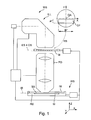
- Fig. 1 shows schematically a microlithographic projection exposure system in the form of a wafer scanner WS, which is provided for fabricating large scale integrated semiconductor components by means of immersion lithography in a step-and-scan mode.
- the projection exposure system comprises as primary radiation source S an Excimer laser having an operating wavelength of 193 nm.
- Other primary radiation sources are used in other embodiments, for example emitting at about 248 nm, 157 nm or 126 nm.
- Radiation sources for the extreme ultraviolet (EUV) spectral range may also be utilized in connection with purely reflective (catoptric) optical systems.
- EUV extreme ultraviolet
- An illumination system ILL optically downstream of the light source generates, in its exit surface ES, a large, sharply delimited, homogeneously illuminated illumination field IF that is adapted to the telecentric requirements of the downstream projection objective PO.
- the illumination system ILL has devices for selection of the illumination mode and, in the example, can be changed over between conventional on-axis illumination with a variable degree of coherence, and off-axis illumination, particularly annular illumination (having a ring shaped illuminated area in a pupil surface of the illumination system) and dipole or quadrupole illumination.
- a device RS for holding and manipulating a mask M in such a way that a pattern formed on the mask lies in the exit surface ES of the illumination system, which coincides with the object surface OS of the projection objective PO.
- the device RS - usually referred to as "reticle stage" - for holding and manipulating the mask contains a mask holder and a scanner drive enabling the mask to be moved parallel to the object surface OS of the projection objective or perpendicular to the optical axis of projection objective and illumination system in a scanning direction (y-direction) during a scanning operation.
- the reduction projection objective PO is designed to image an image of a pattern provided by the mask with a reduced scale of 4:1 onto a wafer W coated with a photoresist layer (magnification
- 0.25).
- Other reduction scales e.g. 5:1 or 8:1 are possible.
- the wafer W serving as a light-sensitive substrate is arranged in such a way that the macroscopically planar substrate surface SS with the photoresist layer essentially coincides with the planar image surface IS of the projection objective.
- the wafer is held by a device WST (wafer stage) comprising a scanner drive in order to move the wafer synchronously with the mask M in parallel with the latter.
- the wafer stage includes z-manipulator means to lift or lower the substrate parallel to the optical axis OA and tilting manipulator means to tilt the substrate about two axes perpendicular to the optical axis.
- the device WST provided for holding the wafer W (wafer stage) is constructed for use in immersion lithography. It comprises a receptacle device RD, which can be moved by a scanner drive and the bottom of which has a flat recess for receiving the wafer W.
- a peripheral edge forms a flat, upwardly open, liquid tight receptacle for a liquid immersion medium IM, which can be introduced into the receptacle and discharged from the latter by means of devices that are not shown.
- the height of the edge is dimensioned in such a way that the immersion medium that has been filled in can completely cover the surface SS of the wafer W and the exit-side end region of the projection objective PO can dip into the immersion liquid given a correctly set operating distance between objective exit and wafer surface.
- the projection objective PO has a planoconvex lens PCL as the last optical element nearest to the image surface IS, the planar exit surface of said lens being the last optical surface of the projection objective PO.
- the exit surface of the last optical element is completely immersed in the immersion liquid IM and is wetted by the latter.
- the exit surface is arranged at a working distance of a few millimetres above the substrate surface SS of the wafer in such a way that there is a gas-filled gap situated between the exit surface of the projection objective and the substrate surface (dry system).
- the illumination system ILL is capable of generating an illumination field having a rectangular shape.
- the size and shape of the illumination field determines the size and shape of the effective object field OF of the projection objective actually used for projecting an image of a pattern on a mask in the image surface of the projection objective.
- the effective object field has a length A* parallel to the scanning direction and a width B* > A* in a cross-scan direction perpendicular to the scanning direction and does not include the optical axis (off-axis field).
- the projection objective PO may include a plurality of schematically indicated lenses (typical numbers of lenses are often more than 10 or more than 15 lenses) and, if appropriate, other transparent optical components.
- the projection objective may be purely dioptric (lenses only).
- the projection objective may include at least one powered mirror, such as at least one concave mirror, in addition to lenses (catadioptric projection objective).
- NA the image-side numerical aperture of the projection objective
- NA ⁇ 1 such as NA ⁇ 1.1 or NA ⁇ 1.2 or NA ⁇ 1.3 or NA ⁇ 1.4 or NA ⁇ 1.5 or NA ⁇ 1.6 NA ⁇ 1.7 or above.
- Typical resolutions down to about 150nm, or 130nm, or 100nm, or 90nm or less are also possible basically depending on the combination of image-side NA and the wavelength of the radiation source.
- the projection objective PO is an optical imaging system designed to form an image of an object arranged in the object surface OS in the image surface, which is optically conjugate to the object surface.
- the imaging may be obtained without forming an intermediate image, or via one or more intermediate images, for example two intermediate images.
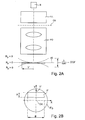
- Petzval curvature Every optical system has associated with it a sort of basic field curvature, which is conventionally called the Petzval curvature, which is now explained in more detail with reference to Fig. 2A .
- the Petzval curvature 1/R P
- the Petzval curvature, 1/R P is given by the Petzval sum 1/R P , which is the reciprocal of the Petzval radius R P , which is the radius of curvature of the Petzval surface.
- the Petzval surface and the paraxial image surface coincide on the optical axis.
- the curvature of the Petzval surface may result in a situation where the Petzval surface departs from the ideal image surface for field points further away from the optical axis.
- the fact that the Petzval surface is curved transforms to a longitudinal departure p of the Petzval surface from the ideal image surface (which is usually flat) at a field point at the outer edge of the image field (at maximum image field height y'), measured parallel to the optical axis in the image space.
- image field curvature is conventionally used to refer to such longitudinal departure (or sag) at maximum image field height y', and may not be confused with the "curvature of the image field”, which is the reciprocal of the radius of curvature of the image field.
- FIG. 2 is purely schematic and not to scale for any of the features discussed in connection with the figure.
- the image field size may be characterized by a maximum image field height y', which corresponds to the radius of the (circular) "design image field" of the objective.
- the design image field IF D includes all field points of the image surface for which the imaging fidelity of the objective is sufficiently good for the intended lithographic process. With other words: all imaging aberrations are corrected sufficiently for the intended application within zones having radial coordinates equal to or smaller than the maximum image field height y', whereas one or more aberrations may be higher than a required threshold value for field points outside the design image field IF D .
- not all field points within the design image field IF D are used for a lithographic process. Instead, exposure is only performed using field points lying within an effective image field IF, which should be sufficiently large in size to allow reasonably sized substrates to be exposed in a lithographic process.
- the effective image field must fit into the design image field IF D in order to include only field points for which the objective is sufficiently corrected and for which no vignetting occurs.
- a slit-shaped effective image field IF is used.
- Fig. 2B shows an example of a rectangular effective off-axis image field IF, which may be utilized in connection with embodiments of obscuration-free catadioptric projection objectives as discussed exemplarily below.
- an effective image field with an arcuate shape (sometimes noted as annular field or ring field) may be used.
- the aspect ratio may be in the range from 2:1 to 10:1, for example.
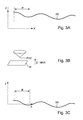
- State-off-the-art scanning projection exposure systems may be equipped with a wafer stage allowing to move the subtrate table parallel to the optical axis (z-manipulation) and also to tilt the wafer table about two mutually perpendicular axes perpendicular to the optical axis (x-tilt and y-tilt).
- the system may be operated to shift and/or tilt the wafer table between exposure steps in order to adjust the position of the substrate surface with respect to the focal region of the projection objective based on previous measurements of the substrate surface (see e.g. US 6,674,510 B1 ).
- Figure 3 shows schematically the conventional principle of a correction using a wafer stage capable of lifting or lowering the substrate surface parallel to the optical axis (z manipulation).
- the wafer stage is lifted in axial direction by a predefined amount (z-MAN)
- the uneven substrate surface may be brought into the region of best focus such that at least parts of the exposure area are in focus, and defocus aberrations are reduced (3C).
- z-MAN predefined amount
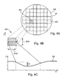
- FIG. 4A shows an axial view of a semiconductor wafer W having a substrate surface SS subdivided in two large number of rectangular exposure areas ES (or dies) arranged in a network of adjacent dies which are successively irradiated via the reticle, one at a time.
- Each exposure area has a width EAX, corresponding to the width of the effective image field of the projection objective in the cross-scan direction (x-direction) and a length EAY which may be equal, larger or smaller than the width EAX and which is substantially greater than the height A of the effective image field.
- Figure 4B shows a vertical section (x-z section) through the substrate showing the multiply curved substrate surface SS. It is contemplated that after global adjustment of the axial position and the tilt angle of the entire substrate the local unevenness of the substrate surface results in a surface profile having an essentially parabolic (quadratic) field profile in x-direction at least in a first approximation.
- the amount of deviation from a planar reference surface may be quantified by the peak-to-valley value pv in the respective area, which is defined here as the difference between minimum and maximum profile height in the exposure area.
- the curvature of the substrate surface SS in the orthogonal y-direction (scanning direction) can be neglected due to the high aspect ratio of the slit-shaped effective image field (for example 4 ⁇ AR ⁇ 6).
- This uneven surface profile of the substrate will therefore induce at least in a first approximation, a quadratic field profile of the defocus and, at the same time, a quadratic field profile of a spherical aberration due to the high image-side numerical aperture of the projection objective. Note that these aberrations are independent of the optical design of the projection objective, and are only dependent from the image-side NA of the projection objective.
- the wavefront aberrations caused by the projection system and/or induced by external conditions are expressed as a linear combination of polynomials.
- polynomials In the optics field, several types of polynomials are available for describing aberrations, for example Seidel polynomials or Zernike polynomials. Zernike polynomials are employed in the following to characterize aberrations.
- Zernike terms to describe wavefront aberrations originating from optical surfaces deviating from being perfectly spherical
- the different Zernike terms signify different aberration phenomena including defocus, astigmatism, coma and spherical aberration up to higher aberrations.
- An aberration may be expressed as a linear combination of a selected number of Zernike polynomials.
- Zernike polynomials are a set of complete orthogonal polynomials defined on a unit circle. Polar coordinates are used, for example with ⁇ being the normalized radius and ⁇ being the azimuth angle.
- a wavefront aberration W( ⁇ , ⁇ ) may be expanded in Zernike polynomials as a sum of products of Zernike terms and respective weighting factors (see e.g. Handbook of Optical Systems: Vol. 2, Physical Image Formation, ed. By H Gross, Wiley-VCH Verlag GmbH & Co. KGaA, Chapter 20.2, (2005 )).
- Zernike polynomials Z1, Z2, Z3 etc. have certain meanings identifying respective contributions to an overall aberration.
- Z3 ⁇ sin ⁇ corresponds to distortion in y direction (or a wavefront tilt in y direction)
- Z5 ⁇ 2 cos2 ⁇ corresponds to astigmatism third order, etc.
- Zernike polynomials may also be used to characterize deviations of an optical surface, such as a lens surface or a mirror surface, from a nominal surface, e.g. a spherical surface.
- Schematic Fig. 6A shows a rectangular exposure area EA on an uneven wafer surface during a scanning operation at two different instant of time. At the first instant of time t 1 the illuminated slit-shaped effective image field IF of the projection objective is positioned close to the lower edge of the exposure area.
- the wafer moves relative to the stationary projection objective in scanning direction (y-direction) such that the illuminated effective image field is at different position spaced apart from the first position at a later instant of time, t 2 .
- the time interval ⁇ t required to cover the entire exposure area with the illuminated image field in one scanning operation may typically range between about 10 ms and 200 ms, for example.
- Figure 6B shows respective sections of the substrate in the x-z-plane perpendicular to the scanning direction.
- the image-side end of the projection objective PO is shown, the exit-side of the projection objective spaced apart by working distance from the uneven substrate surface SS of the substrate.
- the substrate surface has a convex surface shape at t 1
- the substrate surface is concavely curved in a spaced apart region traversed by the projection beam at a later time t 2 >t 1 .
- the dashed line in each case represents the Petzval surface PS of the projection objective, which is adapted to conform to the surface topography of the substrate within the effective image field to allow reducing the imaging aberrations caused by the uneven substrate surface.
- the projection objective is slightly undercorrected with respect to field curvature at the moment t 1 and the correction status is dynamically changed to a slightly overcorrected condition at moment t 2 .
- This significant variation of image field curvature of the imaging system is effective dynamically within fractions of a second adapted to the scanning speed. The variation is effective based on surface topography measurements performed prior to the scanning operation, as explained in more detail below.
- the dynamics of manipulation may be in the order of 20 Hz or more, for example.
- a rate of change in the order of 10% of the depth of focus (DOF) within 10 ms (milliseconds) may be sufficient in many cases to achieve sufficient compensation.
- the defocus is changed with a rate of change between about 0.5% and about 50% of the depth of focus (DOF) of the projection objective within a 1 ms time interval.
- the rate of change of imaging aberrations, such as field curvature and/or distortion, brought about by active manipulation of one ore more optical elements of the projection objective may be orders of magnitude faster than time-dependent changes which may occur during the use of the projection system caused by environmental changes, such as changes of environmental pressure and/or temperature, and/or changes induced by heating of the system.
- the respective exposure systems may be equipped with state-off-the-art manipulators for moving the mask and/or the reticle parallel to the optical axis and for tilting the mask and/or the wafer about one or more tilt axis perpendicular to the optical axis.
- the exposure systems may be equipped with wavelength manipulators to shift the center wavelength ⁇ of the system within a manipulation range ⁇ adapted to the status of chromatic correction of the respective projection objectives.
- one or more additional manipulators are specificially provided to account for effects of substrate surface unevenness and/or unevenness of the reticle, as explained more detailed below.
- Figure 7 shows two axial sections of a first embodiment of a catadioptric projection objective 700.
- Table 7A shows a section in the x-z-plane
- figure 7B shows the respective section in the y-z-plane perpendicular thereto.
- the specification data for the system are taken from the embodiment shown in Fig. 3 of US 2008/0174858 A1 . The corresponding disclosure is incorporated herein by reference.
- Projection objective 700 is designed to project an image of a pattern on a reticle arranged in the planar object surface OS (object plane) into the planar image surface IS (image plane) on a reduced scale, for example, 4:1, while creating exactly two real intermediate images IMI1, IMI2.
- the rectangular effective object field OF and image field IF are off-axis, i.e. entirely outside the optical axis OA.
- a first refractive objective part OP1 is designed for imaging the pattern provided in the object surface into the first intermediate image IMI1.
- a second, catoptric (purely reflective) objective part OP2 images the first intermediate image IMI1 into the second intermediate image IMI2 at a magnification close to 1:(-1).
- a third, refractive objective part OP3 images the second intermediate image IMI2 onto the image surface IS with a strong reduction ratio.
- Projection objective 700 is an example of a "concatenated" projection objective having a plurality of cascaded objective parts which are each configured as imaging systems and are linked via intermediate images, the image (intermediate image) generated by a preceding imaging system in the radiation path serving as object for the succeeding imaging system in the radiation path.
- the succeeding imaging system can generate a further intermediate image (as in the case of the second objective part OP2) or forms the last imaging system of the projection objective, which generates the "final" image field in the image plane of the projection objective (like the third objective part OP3).
- the path of the chief ray CR of an outer field point of the off-axis object field OF is indicated in Fig. 7B in order to facilitate following the beam path of the projection beam.
- a first pupil surface P1 is formed in the first objective part between object surface and first intermediate image
- a second pupil surface P2 is formed in the second objective part between first and second intermediate image
- a third pupil surface P3 is formed in the third objective part between second intermediate image and the image surface IS.
- the second objective part OP2 comprises a first concave mirror CM1 having the concave mirror surface facing the object side, and a second concave mirror CM2 having the concave mirror surface facing the image side.
- the used parts of the mirror surfaces i.e. those areas of the mirror surfaces which are illuminated during operation, are both continuous or unbroken, i.e. the mirrors do not have a hole or bore in the illuminated region.
- the mirror surfaces facing each other define a catadioptric cavity, which is also denoted intermirror space, enclosed by the curved surfaces defined by the concave mirrors.
- the intermediate images IMI1, IMI2 are both situated inside the catadioptric cavity well apart from the mirror surfaces.
- the objective 700 is rotational symmetric and has one straight optical axis OA common to all refractive and reflective optical components ("In-line system"). There are no folding mirrors. An even number of reflections occurs. Object surface and image surface are parallel.
- the concave mirrors have small diameters allowing to arrange them close together and rather close to the intermediate images lying in between.
- the concave mirrors are both constructed and illuminated as off-axis sections of axial symmetric surfaces. The light beam passes by the edges of the concave mirrors facing the optical axis without vignetting. Both concave mirrors are positioned optically remote from a pupil surface rather close to the next intermediate image.
- the objective has an unobscured circular pupil centered around the optical axis thus allowing use as projection objectives for microlithography.
- Both concave mirrors CM1, CM2 are arranged optically close to a field surface formed by the next intermediate image, as indicated by the following table A giving the data for marginal ray height MRH, chief ray height CRH, ray height ratio RHR and sub-aperture ratio SAR: Table A MRH CRH RHR SAR CM1 18.33 -147.93 -8.1 -0.11 CM2 13.68 119.00 +8.7 +0.10
- a position optically close to a field surface may also be characterized by the shape of the projection beam at the respective surface.
- the cross sectional shape of the projection beam deviates significantly from the circular shape typically found in a pupil surface or in proximity thereto.
- the term "projection beam” describes the bundle of all rays running from the effective object field in the object surface towards the effective image field in the image surface.
- Surface positions optically close to a field surface may be defined as positions where the beam diameters of the projection beam in two mutually perpendicular directions orthogonal to the propagation direction of the beam may deviate by more than 50% or more than 100% or more from each other.
- an illuminated area on an optical surface optically close to a field surface will have a shape strongly deviating from a circle end resembling a high aspect ratio rectangle corresponding to a preferred field shape in scanning lithographic projection apparatus.
- the illuminated areas on both the first and second concave mirror are essentially rectangular with rounded edges, the rectangle having about the aspect ratio AR of the effective object and image field.
- the rectangular shape of the effective object field OF may be seen from the comparison between figures 7A and 7B , wherein in Fig. 7A the object field is cut along the long side (x-direction) whereas in figure 7B the object field is cut parallel to the scanning direction i.e. parallel to the short edge of the rectangular effective object field.
- a primary function of the two concave mirrors CM1 and CM2 is to correct the Petzval sum by providing an overcorrecting contribution to Petzval sum counteracting the undercorrecting influence of positive refractive power of lenses.
- the contribution of the concave mirrors to field curvature may be varied dynamically by varying the surface curvature of the reflective surfaces according to a defined spatial and time profile.
- each of the first and second concave mirrors is associated with a mirror manipulator MM1, MM2, respectively, both configured for a two-dimensional deformation (deformation with spatial resolution in two dimensions) of the associated concave mirror during a scanning operation.
- the mirror manipulators may be identical or different in construction.
- each of the concave mirrors has a highly reflective (HR) coating on a flexible portion of a mirror substrate.
- a number of actuators (represented by arrows) of a mirror manipulator MM1 or MM2 are operatively coupled to the back side of the flexible portion.
- the actuators are controlled by a mirror control unit MCU, which may be an integral part of central control unit of the projection exposure apparatus.
- the manipulator control unit is connected to receive signals representing a desired deformation of the mirror surface.
- the mirror manipulator and corresponding control unit may be designed essentially as disclosed in applicants patent applications US 2002/0048096 A1 or US 2005 0280910 A1 (corresponding to WO 03/98350 A2 ), for example. The corresponding disclosures are incorporated into this application by reference.
- any suitable construction of the pupil mirror manipulator may be used instead, for example manipulators using electromechanical actuators, such as piezo-electrical elements, actuators responding to fluid pressure changes, electric and/or magnetic actuators. These actuators may be used to deform a continuous (unbroken) mirror surface as described.
- the mirror manipulator may also include one or more heating elements and/or cooling elements effecting local temperature changes of the mirror leading to a desired deformation of the mirror surface. Resistance heaters or Peltier elements may be used for that purpose.
- a first scenario SC1 the substrate unevenness has been corrected by active manipulation of the wafer z-position and wafer tilt status, basically as explained in connection with Fig 3 , in a conventional manner.
- SC2 a number of active manipulations on optical elements including relative displacements of lenses parallel to the optical axis and tilting of lenses have been performed in addition.
- the overall induced aberrations are decomposed in contributions described by Zernike coefficients, which are shown as the values on the abscissa of Fig. 8 .
- the ordinate shows the scanned aberrations SCA in nm.
- defocus aberration (Z4) and the wavefront tilt aberration (Z2/3) could be reduced significantly both with respect to the standard scenario SC2 and even more reduced with respect to the first scenario SC1, where only an optimization of wafer position with respect to axial position and tilt is used.
- defocus (Z4) and wavefront tilt (Z2/3) can be reduced by about 90% relative to the standard scenario SC2, while even better improvement by about 95% is obtained relative to the pure wafer scenario SC1.
- defocus aberration Z4 could be reduced from about 12nm to about 0.6nm by dynamic deformation of the two concave mirrors.
- a significant improvement is obtained for astigmatism (Z5/6), which could be reduced by about 90% relative to the standard scenario SC2.
- Figure 9 shows schematically the correction deformations applied to the first concave mirror CM1 (Fig. 9A) and second concave mirror CM2 (Fig. 9B) required to obtain the improvement.
- the peak-to-valley (PV) deformations of the reflective surfaces are relatively small and may range in a region below 200nm, for example.
- the PV deformation is about 80nm for CM1 and about 160nm for CM2.
- the figures exemplarily show that relatively long-wave deformations are effective to reduce the aberrations caused by the long-wave quadratic deformation of the substrate surface in the cross-scan direction.
- the compensation mechanism can be implemented in a projection exposure apparatus including a projection objective which has one or more manipulators associated with one or more optical elements of the projection objective by integrating the manipulator(s) into a control system configured to change imaging properties of the projection objective actively during the scanning operation according to a given profile to change dynamically at least aberration of the projection objective between a beginning and an end of the scanning operation.
- the manipulator associates with an optical element may be connected to a control unit generating manipulator control signals which initiate respective changes of the optical effect of the manipulated optical element.
- the manipulator control signals may be generated in different ways.
- a measuring system is provided which allows measuring the surface topography of a substrate surface in a measuring area including the exposure area.
- the substrate surface data may also be derived from data contained in a look-up-table representing a measured or calculated topography of the substrate surface in an area including the exposure area.
- corresponding measures can be implemented to account for non-even surface shape of the reticle.
- Corresponding mask surface data representing a surface profile of the mask in a mask area corresponding to the exposure area may be generated either based on a measurement or based on data from a look-up-table, for example.
- Mask surface data may be processed by the control unit to generate manipulator control signals which are then used to control at least one manipulation device within the projection objective to dynamically adapt the imaging properties of the projection objective in a compensating way to reduce imaging aberrations caused by the surface profile in the mask area.
- NA 1.32.
- the effective image field size is 26 mm by 5.5 mm.
- the specification is given in tables 10, 10A.
- Figure 10A shows a section in the x-z-plane, while Fig. 10B shows the respective section in the y-z-plane perpendicular thereto.
- the specification data for the system are taken from the embodiment shown in Fig. 7 of US 2008/0174858 A1 . The corresponding disclosure is incorporated herein by reference.
- Projection objective 1000 is designed to project an image of a pattern on a reticle arranged in the planar object surface OS (object plane) into the planar image surface IS (image plane) on a reduced scale, for example, 4:1, while creating exactly two real intermediate images IMI1, IMI2.
- the rectangular effective object field OF and image field IF are off-axis, i.e. entirely outside the optical axis OA.
- a first refractive objective part OP1 is designed for imaging the pattern provided in the object surface into the first intermediate image IMI1.
- a second, catadioptric (refractive/reflective) objective part OP2 images the first intermediate image IMI1 into the second intermediate image IMI2 at a magnification close to 1:(-1).
- a third, refractive objective part OP3 images the second intermediate image IMI2 onto the image surface IS with a strong reduction ratio.
- Projection objective 1000 is another example of a "concatenated" projection objective having a plurality of cascaded objective parts which are each configured as imaging systems and are linked via intermediate images, the image (intermediate image) generated by a preceding imaging system in the radiation path serving as object for the succeeding imaging system in the radiation path.
- the sequence is refractive-catadioptric-refractive (R-C-R).
- the path of the chief ray CR of an outer field point of the off-axis object field OF is drawn bold in Fig. 10B in order to facilitate following the beam path of the projection beam.
- a first pupil surface P1 is formed in the first objective part between object surface and first intermediate image
- a second pupil surface P2 is formed in the second objective part between first and second intermediate image
- a third pupil surface P3 is formed in the third objective part between second intermediate image and the image surface IS.
- the second objective part OP2 includes a single concave mirror CM situated at the second pupil surface P2.
- a first planar folding mirror FM1 is arranged optically close to the first intermediate image IMI1 at an angle of 45° to the optical axis OA such that it reflects the radiation coming from the object surface in the direction of the concave mirror CM.
- the folding mirrors FM1, FM2 are each located in the optical vicinity of, but at a small distance from the closest intermediate image. Therefore, the folding mirrors are field mirrors.
- a double pass region where the radiation passes twice in opposite directions is thereby formed geometrically between the deflecting mirrors FM1, FM2 and the concave mirror CM.
- a negative group NG having two negative lenses is arranged in a region with large marginal ray height near the concave mirror and coaxial with the concave mirror such that the radiation passes twice in opposite directions through the negative group.
- No optical element is arranged between the negative group and the concave mirror.
- the first optical element immediately adjacent to the object surface OS is a transparent plane-parallel plate PP arranged very close to the object field.
- Table B gives the data for marginal ray height MRH, chief ray height CRH, ray height ratio RHR and sub-aperture ratio SAR of the entry surface 1 and the exit surface 2 of the plate PP: Table B MRH CRH RHR SAR 1 -39.77 -60.64 +1.5 +0.4 2 -41.50 -60.64 +1.5 +0.4
- the plate is associated with the manipulation device MAN allowing to vary the two-dimensional distribution of refractive index of the plate material in response to electrical signals on a short time scale with high spatial resolution.
- the construction of the manipulator may be based on the wire grid manipulator system disclosed in WO 2008/034636 A2 , which is incorporated herein by reference.
- a cooling system for actively cooling the transparent manipulator element may be provided to increase the dynamics and allow for rapid changes of temperature.
- manipulation may be effected by relative displacement of aspheric surfaces having complementary shape, such as shown, e.g. in EP 0 851 304 B1 .
- a pair of aspheres may be arranged immediately adjacent to the object surface as a field element.
- Electro-optical manipulators may also be utilized.
- a manipulator may be constructed to include cylinder lens elements rotatable relative to each other (see e.g. EP 0 660 169 B1 ), and placed near a field surface, such as the object surface.
- the overall induced aberrations are decomposed in contributions described by Zernike coefficients, which are shown as the values on the abscissa of Fig. 11 .
- the ordinate shows the scanned aberrations in nm. A significant improvement of the scanned aberrations is immediately discernible for the case where the plate-like optical element PP is dynamically activated during the scanning operation to reduce aberrations.
- Both the defocus aberration (Z4) and the wavefront tilt aberration (Z2/3) could be reduced significantly both with respect to the standard scenario SC2 and even more reduced with respect to the first scenario SC1, where only an optimization of wafer position with respect to axial position and tilt is used.
- Both defocus (Z4) and wavefront tilt (Z2/3) can be reduced by about 90% relative to the standard scenario SC2, while even better improvement by about 93% is obtained relative to the pure wafer scenario SC1.
- defocus aberration Z4 could be reduced from about 12nm to about 0.8nm by dynamic modification of reractive index distribution in the plate PP.
- astigmatism (Z5/6) a significant improvement is obtained for astigmatism (Z5/6), which could be reduced by about 90% relative to the standard scenario SC2.
- the parasitic astigmatism aberration Z2/3 is reduced from 0.7nm (in scenario SC2) to 0.3nm in scenario SC3.
- a dynamic change of imaging properties such as field curvature of the projection objective during a scanning operation may significantly improve the aberration level for the entire exposure process in cases where the surface of the substrate to be exposed is not perfectly flat in the exposure area.
- this is only one of many problems which may be solved or induced by providing a projection exposure system with manipulation means allowing a targeted change of the imaging properties of the projection objective during a single scanning operation.
- Another problem which may be addressed by the improved structure and functionality is the problem commonly referred to as "reticle bending".
- the projection objective is aligned with its optical axis in the direction of gravity in typical exposure systems.
- the mask bearing the pattern is then typically oriented in a horizontal plane, perpendicular to the optical axis.
- the reticle may sag owing to the force of gravity, the sagging basically being a function of the type of the reticle and of the mounting technique securing the reticle in a reticle holder.
- the two-dimensional deviation from a planar alignment of the pattern may not be known a priori and may be difficult to determine.
- the problems of aberrations caused by reticle bending may be addressed in a dynamic fashion with embodiments of the exposure apparatus configured to dynamically change the imaging properties of the projection objective during a scanning operation.
- Figure 12 shows qualitatively deformations of a multiply bend reticle surface in a perspective view. If the reticle is held by a support on a frame, the deformation may assume a substantially parabolic shape, as shown, for example, in WO 2006/013100 A2 . If the reticle is mounted by a clamping technique engaging at three or more points in a peripheral region of the reticle, a saddle-shaped deformation may result, which is superimposed on the gravity-induced deformation. Such saddle-shaped deformation is shown in Fig. 12 for a reticle that is clamped at four corner positions.
- the reticle bending may result in a displacement of the center region of the reticle relative to the edge region in the order of one or more tenth of a micrometer. It may be possible to account for a systematic reticle bending effect by counteractive measures during adjustment of a projection objective such that the projection objective has a defined non-zero field curvature which globally accounts for a certain amount of reticle bending.
- non-systematic contributions caused by using different reticles and/or caused by hardly predictable temperature induced deformations during the operation may not be fully accounted for in advance by corresponding adjustment of the projection objective.
- Those non-predictable effects may contribute significantly to the focus budget and it may not be possible to fully account for the corresponding aberration effects by standard manipulations.
- active manipulation of at least one field element in a dynamic fashion during a scanning operation may significantly improve the aberration level towards smaller values.
- Figure 13 shows a comparative view of two correction scenarios.
- the figure shows the residual aberrations after adjustment of the manipulators.
- the columns show the residual errors (scanned aberrations) in a standard scenario SC2 for an anamophotic (saddle-shaped) deformation of the reticle with 400nm PV-deformation at the reticle center.
- the solid line SC3 shows respective values in a correction scenario including targeted deformations of the two concave mirrors CM1, CM2 (field mirrors) of the embodiment of Fig. 7 .
- the defocus value Z4 amounts to about 7nm in a system without correction.
- the defocus error can be reduced to about 3.5nm in the standard scenario SC2.
- Additional targeted deformation of the concave reflective surfaces of mirrors CM 1, CM2 can further reduce the defocus by about an order of magnitude to about 0.3nm.
- the parasitic errors induced by this correction are generally small, such as below 0.5nm as shown.
- FIG. 14 shows a comparative view of three correction scenarios.
- Employing the standard correction allows to reduce residual errors of the focus (Z4) from about 7nm to about 6nm.
- Employing the two-dimensional manipulator acting on a field element close to the object surface allows for significantly reducing those errors.
- the defocus aberration may be reduced from about 6nm to about 0.4nm without introducing parasitic field aberrations above a critical level.
- the tilt error Z2/3 could be been reduced from about 16.8nm in scenario SC1 (Wafer manipulations only) to about 0.6nm with the 2D-manipulator arranged close to the object surface.
- a real-time correction of field aberrations such as field curvature, during a scanning operation in a scanning projection exposure apparatus may significantly reduce imaging aberrations which may be induced by deviations of the substrate surface and/or of the surface of the pattern from the ideal planar shape. Specifically, negative effects of wafer surface unevenness and/or reticle bending in scanning exposure systems may be significantly reduced.
Landscapes
- Physics & Mathematics (AREA)
- General Physics & Mathematics (AREA)
- Lenses (AREA)
- Exposure And Positioning Against Photoresist Photosensitive Materials (AREA)
- Exposure Of Semiconductors, Excluding Electron Or Ion Beam Exposure (AREA)
- Mounting And Adjusting Of Optical Elements (AREA)
Priority Applications (11)
| Application Number | Priority Date | Filing Date | Title |
|---|---|---|---|
| EP09001938A EP2219077A1 (en) | 2009-02-12 | 2009-02-12 | Projection exposure method, projection exposure system and projection objective |
| US12/699,529 US8873022B2 (en) | 2009-02-12 | 2010-02-03 | Projection exposure method, system and objective |
| TW099104346A TWI494705B (zh) | 2009-02-12 | 2010-02-11 | 投射曝光方法、投射曝光系統與投射物鏡 |
| JP2010047084A JP5671243B2 (ja) | 2009-02-12 | 2010-02-12 | 投影露光方法、投影露光システム、及び投影対物系 |
| JP2014147060A JP5923559B2 (ja) | 2009-02-12 | 2014-07-17 | 投影露光方法、投影露光システム、及び投影対物系 |
| US14/496,933 US9036129B2 (en) | 2009-02-12 | 2014-09-25 | Projection exposure method, system and objective |
| US14/683,377 US20150227052A1 (en) | 2009-02-12 | 2015-04-10 | Projection exposure method, system and objective |
| JP2016082705A JP6407193B2 (ja) | 2009-02-12 | 2016-04-18 | 投影露光方法、投影露光システム、及び投影対物系 |
| US15/155,613 US9678440B2 (en) | 2009-02-12 | 2016-05-16 | Projection exposure method, system and objective |
| US15/614,907 US20180059548A1 (en) | 2009-02-12 | 2017-06-06 | Projection exposure method, system and objective |
| JP2018173273A JP2019020739A (ja) | 2009-02-12 | 2018-09-18 | 投影露光方法、投影露光システム、及び投影対物系 |
Applications Claiming Priority (1)
| Application Number | Priority Date | Filing Date | Title |
|---|---|---|---|
| EP09001938A EP2219077A1 (en) | 2009-02-12 | 2009-02-12 | Projection exposure method, projection exposure system and projection objective |
Publications (1)
| Publication Number | Publication Date |
|---|---|
| EP2219077A1 true EP2219077A1 (en) | 2010-08-18 |
Family
ID=40810288
Family Applications (1)
| Application Number | Title | Priority Date | Filing Date |
|---|---|---|---|
| EP09001938A Withdrawn EP2219077A1 (en) | 2009-02-12 | 2009-02-12 | Projection exposure method, projection exposure system and projection objective |
Country Status (4)
| Country | Link |
|---|---|
| US (5) | US8873022B2 (ja) |
| EP (1) | EP2219077A1 (ja) |
| JP (4) | JP5671243B2 (ja) |
| TW (1) | TWI494705B (ja) |
Cited By (1)
| Publication number | Priority date | Publication date | Assignee | Title |
|---|---|---|---|---|
| WO2022156875A1 (en) | 2021-01-19 | 2022-07-28 | Carl Zeiss Smt Gmbh | A method of setting up a projection exposure system, a projection exposure method and a projection exposure system for microlithography |
Families Citing this family (15)
| Publication number | Priority date | Publication date | Assignee | Title |
|---|---|---|---|---|
| EP2219077A1 (en) | 2009-02-12 | 2010-08-18 | Carl Zeiss SMT AG | Projection exposure method, projection exposure system and projection objective |
| CN103443863B (zh) * | 2011-03-23 | 2017-03-08 | 卡尔蔡司Smt有限责任公司 | Euv反射镜布置、包括euv反射镜布置的光学系统以及操作包括euv反射镜布置的光学系统的方法 |
| TWI587077B (zh) * | 2012-03-07 | 2017-06-11 | 尼康股份有限公司 | 光罩、光罩單元、曝光裝置、基板處理裝置、及元件製造方法 |
| DE102012211256A1 (de) | 2012-06-29 | 2014-01-02 | Carl Zeiss Smt Gmbh | Projektionsbelichtungsanlage für die Projektionslithographie |
| US9298102B2 (en) * | 2013-03-13 | 2016-03-29 | Carl Zeiss Smt Gmbh | Projection lens with wavefront manipulator |
| US9651872B2 (en) | 2013-03-13 | 2017-05-16 | Carl Zeiss Smt Gmbh | Projection lens with wavefront manipulator |
| US9690189B2 (en) * | 2013-06-21 | 2017-06-27 | Hoya Corporation | Mask blank substrate, mask blank, transfer mask, and method of manufacturing semiconductor device |
| WO2015032418A1 (en) * | 2013-09-09 | 2015-03-12 | Carl Zeiss Smt Gmbh | Microlithographic projection exposure apparatus and method of correcting optical wavefront deformations in such an apparatus |
| US9516729B2 (en) | 2014-12-16 | 2016-12-06 | Asml Netherlands B.V. | Variable radius mirror dichroic beam splitter module for extreme ultraviolet source |
| DE102015218329A1 (de) | 2015-09-24 | 2017-03-30 | Carl Zeiss Smt Gmbh | Optische Korrekturanordnung, Projektionsobjektiv mit einer solchen optischen Korrekturanordnung sowie mikrolithografische Apparatur mit einem solchen Projektionsobjektiv |
| DE102016205072A1 (de) * | 2016-03-29 | 2017-03-16 | Carl Zeiss Smt Gmbh | Optisches System für die Mikrolithografie sowie Verfahren zum Betreiben eines optischen Systems für die Mikrolithografie |
| WO2018028971A1 (en) * | 2016-08-11 | 2018-02-15 | Asml Holding N.V. | Variable corrector of a wave front |
| JP6951446B2 (ja) * | 2016-12-20 | 2021-10-20 | エーファウ・グループ・エー・タルナー・ゲーエムベーハー | 感光性の層を露光するための装置および方法 |
| NL2024451A (en) * | 2019-01-18 | 2020-08-14 | Asml Netherlands Bv | Projection system and lithographic apparatus comprising said projection system |
| JP7178932B2 (ja) * | 2019-03-12 | 2022-11-28 | キヤノン株式会社 | 露光装置、および物品製造方法 |
Citations (15)
| Publication number | Priority date | Publication date | Assignee | Title |
|---|---|---|---|---|
| WO1999032940A1 (en) | 1997-12-22 | 1999-07-01 | Asm Lithography B.V. | Repetitively projecting a mask pattern using a time-saving height measurement |
| EP0660169B1 (en) | 1993-12-22 | 2000-04-26 | Nikon Corporation | Projection exposure apparatus |
| US20020048096A1 (en) | 2000-09-20 | 2002-04-25 | Frank Melzer | Optical element deformation system |
| US20030090640A1 (en) * | 2001-11-02 | 2003-05-15 | Tadahito Fujisawa | Exposure method and apparatus |
| US20030133087A1 (en) | 2002-01-08 | 2003-07-17 | Canon Kabushiki Kaisha | Scanning exposure apparatus, manufacturing method thereof, and device manufacturing method |
| WO2003098350A2 (de) | 2002-05-18 | 2003-11-27 | Carl Zeiss Smt Ag | Verfahren zur gezielten deformation eines optischen elements |
| US20030234918A1 (en) | 2002-06-20 | 2003-12-25 | Nikon Corporation | Adjustable soft mounts in kinematic lens mounting system |
| US6674510B1 (en) | 1999-03-08 | 2004-01-06 | Asml Netherlands B.V. | Off-axis levelling in lithographic projection apparatus |
| EP0851304B1 (en) | 1996-12-28 | 2004-03-17 | Canon Kabushiki Kaisha | Projection exposure apparatus and device manufacturing method |
| WO2006001300A1 (ja) | 2004-06-23 | 2006-01-05 | Daiso Co., Ltd. | 高耐久性液体クロマトグラフィー用充填剤 |
| WO2006013100A2 (en) | 2004-08-06 | 2006-02-09 | Carl Zeiss Smt Ag | Projection objective for microlithography |
| US20060256314A1 (en) * | 2005-05-13 | 2006-11-16 | Christoph Nolscher | Method for exposing a semiconductor wafer |
| WO2008034636A2 (de) | 2006-09-21 | 2008-03-27 | Carl Zeiss Smt Ag | Optisches element und verfahren |
| US7385756B2 (en) | 2004-01-14 | 2008-06-10 | Carl Zeiss Smt Ag | Catadioptric projection objective |
| US20080174858A1 (en) | 2007-01-23 | 2008-07-24 | Carl Zeiss Smt Ag | Projection objective for lithography |
Family Cites Families (37)
| Publication number | Priority date | Publication date | Assignee | Title |
|---|---|---|---|---|
| US4226507A (en) | 1979-07-09 | 1980-10-07 | The Perkin-Elmer Corporation | Three actuator deformable specimen |
| US4647164A (en) | 1985-11-21 | 1987-03-03 | The United States Of America As Represented By The United States Department Of Energy | Apparatus for and method of correcting for astigmatism in a light beam reflected off of a light reflecting surface |
| JP3303758B2 (ja) * | 1996-12-28 | 2002-07-22 | キヤノン株式会社 | 投影露光装置及びデバイスの製造方法 |
| JPH1145846A (ja) | 1997-07-25 | 1999-02-16 | Nikon Corp | 走査型露光方法及び装置 |
| US7112772B2 (en) | 1998-05-29 | 2006-09-26 | Carl Zeiss Smt Ag | Catadioptric projection objective with adaptive mirror and projection exposure method |
| DE19824030A1 (de) | 1998-05-29 | 1999-12-02 | Zeiss Carl Fa | Katadioptrisches Projektionsobjektiv mit adaptivem Spiegel und Projektionsbelichtungsverfahren |
| JPH11354410A (ja) * | 1998-06-09 | 1999-12-24 | Sony Corp | 露光装置および露光方法 |
| JP2000019165A (ja) | 1998-06-30 | 2000-01-21 | Shimadzu Corp | ガスクロマトグラフ装置 |
| TW575771B (en) * | 2000-07-13 | 2004-02-11 | Asml Netherlands Bv | Lithographic apparatus, device manufacturing method, and device manufactured thereby |
| JP2002037545A (ja) | 2000-07-26 | 2002-02-06 | Matsushita Electric Works Ltd | エレベータのブレーキ制御回路 |
| AU2002210978A1 (en) | 2000-10-31 | 2002-05-15 | Nikon Corporation | Exposure method and system |
| JP2004056125A (ja) | 2002-06-20 | 2004-02-19 | Nikon Corp | 個別アクチュエータを有する反射投影光学系 |
| US6880942B2 (en) | 2002-06-20 | 2005-04-19 | Nikon Corporation | Adaptive optic with discrete actuators for continuous deformation of a deformable mirror system |
| US7158215B2 (en) | 2003-06-30 | 2007-01-02 | Asml Holding N.V. | Large field of view protection optical system with aberration correctability for flat panel displays |
| US7196772B2 (en) | 2003-11-07 | 2007-03-27 | Asml Netherlands B.V. | Lithographic apparatus and device manufacturing method |
| CN1902733A (zh) * | 2004-01-06 | 2007-01-24 | 株式会社尼康 | 曝光方法和装置以及器件制造方法 |
| JP4843272B2 (ja) | 2004-07-31 | 2011-12-21 | カール・ツァイス・エスエムティー・ゲーエムベーハー | マイクロリソグラフィ投影露光装置の光学システム |
| FR2877104B1 (fr) | 2004-10-27 | 2006-12-29 | Sagem | Dispositif d'imagerie ou d'insolation, notamment pour la realisation d'un micro-circuit electronique |
| US7184124B2 (en) | 2004-10-28 | 2007-02-27 | Asml Holding N.V. | Lithographic apparatus having an adjustable projection system and device manufacturing method |
| JP4980922B2 (ja) * | 2004-11-18 | 2012-07-18 | カール・ツァイス・エスエムティー・ゲーエムベーハー | マイクロリソグラフィ投影露光装置及びマイクロリソグラフィ投影露光装置の像面湾曲を修正するための方法 |
| JP4817702B2 (ja) * | 2005-04-14 | 2011-11-16 | キヤノン株式会社 | 光学装置及びそれを備えた露光装置 |
| CN100474115C (zh) * | 2006-04-04 | 2009-04-01 | 上海微电子装备有限公司 | 光刻机成像光学系统像差现场测量方法 |
| US8197076B2 (en) * | 2006-05-11 | 2012-06-12 | Massachusetts Institute Of Technology | Magnetic membrane mirror |
| DE102006024810A1 (de) | 2006-05-27 | 2007-11-29 | Carl Zeiss Smt Ag | Mikrolithographische Projektionsbelichtungsanlage sowie adaptiver Spiegel hierfür |
| EP1890191A1 (en) * | 2006-08-14 | 2008-02-20 | Carl Zeiss SMT AG | Catadioptric projection objective with pupil mirror |
| US20090042139A1 (en) | 2007-04-10 | 2009-02-12 | Nikon Corporation | Exposure method and electronic device manufacturing method |
| US20090042115A1 (en) | 2007-04-10 | 2009-02-12 | Nikon Corporation | Exposure apparatus, exposure method, and electronic device manufacturing method |
| DE102008001800A1 (de) | 2007-05-25 | 2008-11-27 | Carl Zeiss Smt Ag | Projektionsobjektiv für die Mikrolithographie, Mikrolithographie-Projektionsbelichtungsanlage mit einem derartigen Projektionsobjektiv, mikrolithographisches Herstellungsverfahren für Bauelemente sowie mit diesem Verfahren hergestelltes Bauelement |
| JP2008292801A (ja) * | 2007-05-25 | 2008-12-04 | Canon Inc | 露光装置および方法 |
| US8440375B2 (en) | 2007-05-29 | 2013-05-14 | Nikon Corporation | Exposure method and electronic device manufacturing method |
| JP5406437B2 (ja) * | 2007-06-22 | 2014-02-05 | キヤノン株式会社 | 露光装置及びデバイス製造方法 |
| JP5033724B2 (ja) * | 2007-07-12 | 2012-09-26 | 株式会社沖データ | 文書検索装置及び画像形成装置、文書検索システム |
| WO2009013230A1 (en) * | 2007-07-23 | 2009-01-29 | Carl Zeiss Smt Ag | Optical system of a microlithographic projection exposure apparatus |
| EP2188673A1 (en) | 2007-08-03 | 2010-05-26 | Carl Zeiss SMT AG | Projection objective for microlithography, projection exposure apparatus, projection exposure method and optical correction plate |
| US7993780B2 (en) | 2007-10-05 | 2011-08-09 | Nanotek Instruments, Inc. | Process for producing carbon anode compositions for lithium ion batteries |
| JP5105474B2 (ja) * | 2007-10-19 | 2012-12-26 | 国立大学法人東京農工大学 | 露光装置及びデバイス製造方法 |
| EP2219077A1 (en) | 2009-02-12 | 2010-08-18 | Carl Zeiss SMT AG | Projection exposure method, projection exposure system and projection objective |
-
2009
- 2009-02-12 EP EP09001938A patent/EP2219077A1/en not_active Withdrawn
-
2010
- 2010-02-03 US US12/699,529 patent/US8873022B2/en active Active
- 2010-02-11 TW TW099104346A patent/TWI494705B/zh active
- 2010-02-12 JP JP2010047084A patent/JP5671243B2/ja active Active
-
2014
- 2014-07-17 JP JP2014147060A patent/JP5923559B2/ja active Active
- 2014-09-25 US US14/496,933 patent/US9036129B2/en active Active
-
2015
- 2015-04-10 US US14/683,377 patent/US20150227052A1/en not_active Abandoned
-
2016
- 2016-04-18 JP JP2016082705A patent/JP6407193B2/ja active Active
- 2016-05-16 US US15/155,613 patent/US9678440B2/en active Active
-
2017
- 2017-06-06 US US15/614,907 patent/US20180059548A1/en active Pending
-
2018
- 2018-09-18 JP JP2018173273A patent/JP2019020739A/ja not_active Abandoned
Patent Citations (16)
| Publication number | Priority date | Publication date | Assignee | Title |
|---|---|---|---|---|
| EP0660169B1 (en) | 1993-12-22 | 2000-04-26 | Nikon Corporation | Projection exposure apparatus |
| EP0851304B1 (en) | 1996-12-28 | 2004-03-17 | Canon Kabushiki Kaisha | Projection exposure apparatus and device manufacturing method |
| WO1999032940A1 (en) | 1997-12-22 | 1999-07-01 | Asm Lithography B.V. | Repetitively projecting a mask pattern using a time-saving height measurement |
| US6674510B1 (en) | 1999-03-08 | 2004-01-06 | Asml Netherlands B.V. | Off-axis levelling in lithographic projection apparatus |
| US20020048096A1 (en) | 2000-09-20 | 2002-04-25 | Frank Melzer | Optical element deformation system |
| US20030090640A1 (en) * | 2001-11-02 | 2003-05-15 | Tadahito Fujisawa | Exposure method and apparatus |
| US20030133087A1 (en) | 2002-01-08 | 2003-07-17 | Canon Kabushiki Kaisha | Scanning exposure apparatus, manufacturing method thereof, and device manufacturing method |
| WO2003098350A2 (de) | 2002-05-18 | 2003-11-27 | Carl Zeiss Smt Ag | Verfahren zur gezielten deformation eines optischen elements |
| US20050280910A1 (en) | 2002-05-18 | 2005-12-22 | Fehr Jean N | Method for the targeted deformation of an optical element |
| US20030234918A1 (en) | 2002-06-20 | 2003-12-25 | Nikon Corporation | Adjustable soft mounts in kinematic lens mounting system |
| US7385756B2 (en) | 2004-01-14 | 2008-06-10 | Carl Zeiss Smt Ag | Catadioptric projection objective |
| WO2006001300A1 (ja) | 2004-06-23 | 2006-01-05 | Daiso Co., Ltd. | 高耐久性液体クロマトグラフィー用充填剤 |
| WO2006013100A2 (en) | 2004-08-06 | 2006-02-09 | Carl Zeiss Smt Ag | Projection objective for microlithography |
| US20060256314A1 (en) * | 2005-05-13 | 2006-11-16 | Christoph Nolscher | Method for exposing a semiconductor wafer |
| WO2008034636A2 (de) | 2006-09-21 | 2008-03-27 | Carl Zeiss Smt Ag | Optisches element und verfahren |
| US20080174858A1 (en) | 2007-01-23 | 2008-07-24 | Carl Zeiss Smt Ag | Projection objective for lithography |
Non-Patent Citations (2)
| Title |
|---|
| "Physical Image Formation", 2005, WILEY-VCH VERLAG GMBH & CO., article "e.g. Handbook of Optical Systems" |
| H.W. VAN ZEIJL ET AL.: "Lithographic Alignment Offset Compensation for Substrate Transfer Process", PROC. STW/SAFE, 2005, pages 121 - 126 |
Cited By (1)
| Publication number | Priority date | Publication date | Assignee | Title |
|---|---|---|---|---|
| WO2022156875A1 (en) | 2021-01-19 | 2022-07-28 | Carl Zeiss Smt Gmbh | A method of setting up a projection exposure system, a projection exposure method and a projection exposure system for microlithography |
Also Published As
| Publication number | Publication date |
|---|---|
| JP5671243B2 (ja) | 2015-02-18 |
| US20160320707A1 (en) | 2016-11-03 |
| US9036129B2 (en) | 2015-05-19 |
| JP2016164675A (ja) | 2016-09-08 |
| TW201104358A (en) | 2011-02-01 |
| US20150227052A1 (en) | 2015-08-13 |
| JP2014239240A (ja) | 2014-12-18 |
| JP2010187002A (ja) | 2010-08-26 |
| US9678440B2 (en) | 2017-06-13 |
| JP2019020739A (ja) | 2019-02-07 |
| US8873022B2 (en) | 2014-10-28 |
| JP5923559B2 (ja) | 2016-05-24 |
| JP6407193B2 (ja) | 2018-10-17 |
| TWI494705B (zh) | 2015-08-01 |
| US20100201962A1 (en) | 2010-08-12 |
| US20180059548A1 (en) | 2018-03-01 |
| US20150049320A1 (en) | 2015-02-19 |
Similar Documents
| Publication | Publication Date | Title |
|---|---|---|
| US9678440B2 (en) | Projection exposure method, system and objective | |
| US8390784B2 (en) | Catadioptric projection objective with pupil mirror, projection exposure apparatus and projection exposure method | |
| EP1712955B1 (en) | Optical unit and exposure apparatus having the same | |
| JP4536088B2 (ja) | リソグラフィック装置、収差補正デバイス、およびデバイス製造方法 | |
| US7800732B2 (en) | Projection exposure method and projection exposure apparatus for microlithography | |
| KR101428136B1 (ko) | 마이크로리소그래피용 투사 대물렌즈, 투사 노광 장치, 투사 노광 방법 및 광학 보정 플레이트 | |
| US9581813B2 (en) | Method for improving the imaging properties of a projection objective, and such a projection objective | |
| EP1246014A1 (en) | Lithographic apparatus | |
| EP1580605B1 (en) | Method of determining aberration of a projection system of a lithographic apparatus | |
| JP2001289735A (ja) | 光学像形成系における収差を測定する方法 | |
| US20200371444A1 (en) | Projection exposure method and projection exposure apparatus for microlithography | |
| EP1251402A1 (en) | Lithographic apparatus | |
| US20140268084A1 (en) | Projection lens with wavefront manipulator | |
| EP1927891A1 (en) | Projection objective with conjugated pupils | |
| US20060046165A1 (en) | Lithographic apparatus, device manufacturing method, calibration method and computer program product | |
| WO2016134862A1 (en) | Lithographic apparatus, manipulator system and method of controlling curvature of a focal plane |
Legal Events
| Date | Code | Title | Description |
|---|---|---|---|
| PUAI | Public reference made under article 153(3) epc to a published international application that has entered the european phase |
Free format text: ORIGINAL CODE: 0009012 |
|
| AK | Designated contracting states |
Kind code of ref document: A1 Designated state(s): AT BE BG CH CY CZ DE DK EE ES FI FR GB GR HR HU IE IS IT LI LT LU LV MC MK MT NL NO PL PT RO SE SI SK TR |
|
| AX | Request for extension of the european patent |
Extension state: AL BA RS |
|
| AKY | No designation fees paid | ||
| STAA | Information on the status of an ep patent application or granted ep patent |
Free format text: STATUS: THE APPLICATION IS DEEMED TO BE WITHDRAWN |
|
| 18D | Application deemed to be withdrawn |
Effective date: 20110219 |