EP2216902A1 - Vorspannungsschaltung und verfahren zur steuerung einer vorspannungsschaltung - Google Patents
Vorspannungsschaltung und verfahren zur steuerung einer vorspannungsschaltung Download PDFInfo
- Publication number
- EP2216902A1 EP2216902A1 EP07828024A EP07828024A EP2216902A1 EP 2216902 A1 EP2216902 A1 EP 2216902A1 EP 07828024 A EP07828024 A EP 07828024A EP 07828024 A EP07828024 A EP 07828024A EP 2216902 A1 EP2216902 A1 EP 2216902A1
- Authority
- EP
- European Patent Office
- Prior art keywords
- transistor
- gate
- bias
- bias circuit
- transistors
- Prior art date
- Legal status (The legal status is an assumption and is not a legal conclusion. Google has not performed a legal analysis and makes no representation as to the accuracy of the status listed.)
- Granted
Links
Images


Classifications
-
- H—ELECTRICITY
- H03—ELECTRONIC CIRCUITRY
- H03F—AMPLIFIERS
- H03F1/00—Details of amplifiers with only discharge tubes, only semiconductor devices or only unspecified devices as amplifying elements
- H03F1/08—Modifications of amplifiers to reduce detrimental influences of internal impedances of amplifying elements
- H03F1/22—Modifications of amplifiers to reduce detrimental influences of internal impedances of amplifying elements by use of cascode coupling, i.e. earthed cathode or emitter stage followed by earthed grid or base stage respectively
- H03F1/223—Modifications of amplifiers to reduce detrimental influences of internal impedances of amplifying elements by use of cascode coupling, i.e. earthed cathode or emitter stage followed by earthed grid or base stage respectively with MOSFET's
-
- H—ELECTRICITY
- H03—ELECTRONIC CIRCUITRY
- H03F—AMPLIFIERS
- H03F1/00—Details of amplifiers with only discharge tubes, only semiconductor devices or only unspecified devices as amplifying elements
- H03F1/30—Modifications of amplifiers to reduce influence of variations of temperature or supply voltage or other physical parameters
- H03F1/301—Modifications of amplifiers to reduce influence of variations of temperature or supply voltage or other physical parameters in MOSFET amplifiers
-
- H—ELECTRICITY
- H03—ELECTRONIC CIRCUITRY
- H03F—AMPLIFIERS
- H03F2200/00—Indexing scheme relating to amplifiers
- H03F2200/108—A coil being added in the drain circuit of a FET amplifier stage, e.g. for noise reducing purposes
-
- H—ELECTRICITY
- H03—ELECTRONIC CIRCUITRY
- H03F—AMPLIFIERS
- H03F2200/00—Indexing scheme relating to amplifiers
- H03F2200/18—Indexing scheme relating to amplifiers the bias of the gate of a FET being controlled by a control signal
-
- H—ELECTRICITY
- H03—ELECTRONIC CIRCUITRY
- H03F—AMPLIFIERS
- H03F2200/00—Indexing scheme relating to amplifiers
- H03F2200/456—A scaled replica of a transistor being present in an amplifier
Definitions
- the present invention relates to a bias circuit and a control method for a bias circuit.
- a bias circuit is connected to an amplifier and applies a constant bias voltage with respect to an input signal to the amplifier.
- a circuit 100 illustrated in FIG. 7 includes a constant-current source (CS1) 101, first and second transistors (MN1, MN2) 102, 104, and resistor 103.
- a bias circuit is configured by the constant-current source (CS1) 101 and the first transistor (MN1) and applies a bias voltage to an amplifier configured by a coil 106 and a transistor (MN3) 105.
- Patent Document 1 Japanese Laid-Open Patent Publication No. H9-148853 .
- Patent Document 2 Japanese Laid-Open Patent Publication No. H11-234060 .
- Patent Document 3 International Publication Pamphlet No. WO 01/08299 A1 .
- the gate length of the first transistor (MN1) 102 may be made less than the gate length of the second transistor (MN2) 104 in order to apply Vth (threshold voltage) to the gate of the second transistor (MN2) 104.
- Vth threshold voltage
- a characteristics of the amplifier is restricted because the transistor (MN2) 104 with a large gate length is used regardless of the possibility of producing the transistor (MN1) 102 with a small gate length in the transistor production process.
- the first and second transistors (MN1, MN2) 102, 104 have different gate lengths, the effect of production spread is easily demonstrated, the bias accuracy is degraded, and the yield is reduced.
- Vth + ⁇ is taken as a bias voltage with respect to the threshold voltage Vth.
- Vth + ⁇ is applied as the bias voltage
- a B-class amplifier does not operate as the B-class amplifier. This is because it starts operating as the B-class amplifier after the threshold voltage Vth has been applied. It is desirable to configure a bias circuit that will apply the threshold voltage Vth to an amplifier with nonlinear input and output, such as the B-class amplifier.
- Another object of the present invention is to provide a bias circuit and control method for a bias circuit that can operate at a high speed.
- Yet another object of the present invention is to provide a bias circuit and control method for a bias circuit that can apply a threshold voltage Vth to a nonlinear amplifier.
- a bias circuit for applying a bias voltage to a nonlinear amplification circuit, including a constant-current source; and a first, second, third, and fourth transistors, wherein a current mirror circuit is configured by the first transistor and the second transistor, a drain and gate of the third transistor and a gate of the fourth transistor are connected, the first transistor and the third transistor are cascade connected, the second transistor and the fourth transistor are cascade connected, and the bias voltage is outputted from the drain of the second transistor, gate lengths and gate widths of the first and second transistor are the same, gate lengths of the first to fourth transistor are the same, and gate lengths and gate widths of the first, second, third, and fourth transistor are configured so that k 4 -0.5 - k 3 -0.5 is approximately 1, where k 3 stands for a ratio of a gate width of the third transistor to the gate width of the first transistor and k 4 stands for a ratio of a gate width of the fourth transistor to the gate width of the first transistor.
- a control method for a bias circuit that applies a bias voltage to a nonlinear amplification circuit including detecting an output power from the nonlinear amplification circuit, and controlling ON or OFF of transistor constituting the bias circuit on the basis of the output power so that the output power becomes a set power.
- the present invention can provide a bias circuit and control method for a bias circuit in which fluctuations of characteristics are inhibited.
- the present invention can also provide a bias circuit and control method for a bias circuit that can operate at a high speed. Further, the present invention can also provide a bias circuit and control method for a bias circuit that can apply a threshold voltage Vth to a nonlinear amplifier.
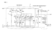
- FIG. 1 illustrates configuration examples of a bias circuit, a B-class amplification circuit, and a control unit.
- FIG. 1 illustrates configuration examples of a bias circuit 10, a B-class amplification circuit 50, and a control unit 60.
- the bias circuit 10 includes a first to third p-channel transistors (referred to hereinbelow as p-type transistors) (MP1, MP2, MP3) 11, 12, 13, a constant-current source 14, a resistor 15, a capacitor 16, a first and second n-channel transistors (referred to hereinbelow as n-type transistors) (MN1, MN2) 21, 22, and a fourth to k-th n-type transistors (MN4, MN5, ..., MNk; k is integer equal to or greater than 7) 24, 25, 26, 27.
- the bias circuit 10 serves to apply a bias voltage to the B-class amplification circuit 50.
- the B-class amplification circuit 50 includes a coil 51, a (k + 1) -th n-type transistor (MN(k + 1)) 52, and a third n-type transistor (MN3) 53.
- the B-class amplification circuit 50 is a nonlinear amplification circuit that amplifies only one polarity of inputted signals. An output signal of the circuit is obtained only when the input voltage is positive.
- the control unit 60 includes a detection circuit 61 and a control circuit 62.
- the control unit 60 controls the bias circuit 10 so as to compensate a spread in the output signal outputted from the B-class amplification circuit 50.
- the bias circuit 10 applies the bias voltage so as to obtain the threshold voltage Vth at the gate of the third n-type transistor 53 of the B-class amplification circuit 50. How to configure the bias circuit 10 in order to enable the output of the threshold voltage Vth will be explained in detail below.
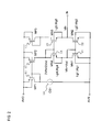
- FIG. 2 illustrates a basic configuration example of the bias circuit 10 in FIG. 1 . Common components are assigned with like reference numerals.
- the gate of the first p-type transistor (MP1) 11 and the gate of the second p-type transistor (MP2) 12 are connected to each other, and the drain of the first p-type transistor (MP1) 11 is connected to the constant-current source 14. Further, the sources of the first to third p-type transistors (MP1, MP2, MP3) 11, 12, 13 are connected to the supply power source (AVD).
- the gates of the fourth n-type transistor (MN4) 24 and the fifth n-type transistor (MN5) 25 are connected to each other to configure a current mirror circuit.
- a current mirror circuit is also constituted by the first n-type transistor (MN1) 21 and the second n-type transistor (MN2) 22. These two current mirror circuits are cascade connected.
- the drain of the second p-type transistor (MP2) 12 and the drain of the fourth n-type transistor (MN4) 24 are connected to each other, and the drain of the fifth n-type transistor (MN5) 25 and the drain of the third p-type transistor (MP3) 13 are connected to each other.
- An IN terminal is connected between the drain of the second n-type transistor (MN2) 22 and the source of the fifth n-type transistor (MN5) 25, and a bias voltage is outputted from the IN terminal to the third n-type transistor (MN3) 53.
- the first, second, and fourth n-type transistors 21, 22, 24 are configured to have the same size (same gate length and same gate width).
- the fifth n-type transistor 25 is so configured that the gate length thereof is equal to those of other transistors 21, 22, 24, but the gate width is approximately 1/4 that of other transistors 21, 22, 24.
- the gate length of the third n-type transistor (MN3) 53 of the B-class amplification circuit 50 is equal to those of the first, second, and fourth n-type transistors 21, 22, 24.
- the threshold voltage Vth of the third n-type transistor (MN3) 53 is outputted from the IN terminal.
- Vod Vg - Vth
- Co is a gate capacity per unit surface area
- ⁇ is a mobility
- k is a constant.
- Vod is generally called “an overdrive voltage”, and indicates the increase in gate bias Vg with respect to the threshold voltage Vth.
- a drain current Id2 of the second n-type transistor 22 can be found in the following manner by using the Formula 4.
- Id ⁇ 2 k Wg ⁇ 2 / Lg ⁇ 2 ⁇ Vod ⁇ 2 2
- Vod2 indicates an overdrive voltage of the second n-type transistor 22.
- Vod5 indicates an overdrive voltage of the fifth n-type transistor 25.
- a gate voltage Vg1 applied to the gate of the first n-type transistor 21 can be represented by the following formula on the basis of the Formula 6.
- Vg ⁇ 1 Vod ⁇ 1 + Vth
- the threshold voltage is the same Vth.
- Vg5 of the fifth n-type transistor 25 Vod ⁇ 5 + Vth + VIN
- the threshold voltage of the fifth n-type transistor 25 in the Formula 13 becomes the same Vth.
- VIN 2 ⁇ Vod ⁇ 1 + 2 ⁇ Vth - Vod ⁇ 5 + Vth
- the bias circuit 10 can output from the IN terminal a bias voltage that is equal to the threshold voltage Vth of the third n-type transistor 53.
- the production spread easily occurs when transistors of different gate length Lg are produced, but the production spread hardly occurs when transistors of the same gate length Lg and different gate width Wg are produced. Therefore, because four transistors 21, 22, 24, 25 of the bias circuit 10 have the same gate length Lg, the fluctuation of characteristics caused by production spread can be inhibited.
- the gate width of the fifth transistor 25 is set to approximately 1/4 that of other transistors will be considered below.
- the current flowing from the second p-type transistor (MP2) 12 to the first n-type transistor 21 has the same value as the current flowing from the third p-type transistor (MP3) 13 to the second n-type transistor 22.
- the first, second, fourth, and fifth n-type transistors (MN1, MN2, MN4, MN5) 21, 22, 24, 25 have the same gate length Lg. Therefore, based on the Formula 4, the following relationship is valid: Vod ⁇ 1 / ⁇ Wg
- the Formula 18 indicates that the gate width Wg5 of the fifth transistor 25 may be configured such that the difference between the overdrive voltages Vod4 and Vod5 of the fourth and fifth transistors 24, 25 becomes equal to the overdrive voltage Vod1 of the first transistor 21.
- the gate width Wg4 of the fourth transistor 24 is "1" (same as the gate width Wg1 of the first transistor 21) and the gate width Wg5 of the fifth transistor 25 is "1/4" (1/4 of the gate width Wg1 of the first transistor 21).
- the gate width Wg4 is "2" (the gate width Wg of the first transistor 21 is “2” and is twice as large as the gate width Wg1 of the first transistor 21) and the gate width Wg5 of the fifth transistor 25 is "1/3" (1/3 of the gate width Wg1). This is because ( ⁇ 3 - 1/ ⁇ 2) ⁇ 1 and the Formula 18 is satisfied.
- the gate widths Wg1, Wg4, Wg5 of the transistors 21, 24, 25 may be provided such that the following relationship is satisfied: k 4 - 0.5 - k 3 - 0.5 ⁇ 1 where k 3 stands for a ratio of the gate width Wg4 of the fourth transistor (MN4) to the gate width Wg1 of the first transistor (MN1) 21 and k 4 stands for a ratio of the gate width Wg5 of the fifth transistor (MN5) to the gate width Wg1 of the second transistor (MN1) 21.
- the bias circuit 10 illustrated in FIG. 1 is configured by arranging sixth to k-th (k is integer equal to or greater than 7) n-type transistors (MN6, ..., Mnk) 26, 27 in parallel to the fifth n-type transistor 25.
- drains of the fifth to k-th n-type transistors 25, 26, 27 are connected to each other, and gates of these transistors are connected to each other, and control signals of the control unit 60 are inputted to these transistors 25, 26, 27.
- the gate length of the sixth to k-the n-type transistors 26, 27 is equal to that of the fifth n-type transistor 25.
- the ratio of the gate widths of these transistors may be constituted by a ratio represented by a power of 2.
- the control unit 60 can change the gate width of the fifth n-type transistor 25 illustrated in FIG. 2 .
- the bias voltage outputted from the bias circuit 10 can be varied in the vicinity of the threshold Vth. This will be explained below in greater detail.
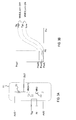
- FIG. 3A illustrates a configuration example of the B-class amplification circuit 50.
- FIG. 3B is a graph illustrating an example of relationship between an input power Pin and output power Pout in the B-class amplification circuit 50.
- constituent components identical to those in FIG. 1 are assigned with like reference numerals.
- the output power Pout changes from PoutL to PoutH (PoutL ⁇ PoutH) due to the production spread.
- the bias point provided to the B-class amplification circuit 50 is controlled so as to be low and obtain the set power Pout0 by switching OFF the fifth to k-th n-type transistors (MN5, ..., MNk) 25, 26, 27 in FIG. 1 .
- the bias point is controlled so as to be raise and obtain the set power Pout0 by switching ON the fifth to k-th n-type transistors (MN5, ..., Mnk) 25, 26, 27.
- Such the control can inhibit the fluctuations.
- FIG. 4 is a flowchart illustrating an example of control procedure in the control unit 60.
- a test signal is inputted from the input terminal IN ( FIG. 1 or FIG. 3A ), and the detection circuit 61 of the control unit 60 detects the power Pout of the output signal (S11).
- the detection circuit 61 outputs the value of the detected output power Pout to the control circuit 62.
- control circuit 62 compares the output power Pout with the set power Pout0 (S13), and when the output power Pout is higher than the set power Pout0 (S14), the control circuit outputs a control signal that switches OFF the fifth to k-th n-type transistors (MN5, ..., MNk) 25, 26, 27, to each of the transistors 25, 26, 27 (S15).
- control circuit 62 ends the processing, without outputting the control signal (S17).
- control circuit 62 outputs a control signal that switches ON the fifth to k-th n-type transistors 25, 26, 27, to each of the transistors 25, 26, 27 (S19).
- the output power Pout that is outputted by the B-class amplification circuit 50 becomes the set power Pout0, and the fluctuations of characteristics induced by the production spread can be inhibited not only for the transistors 21 of the bias circuit 10, but also for the transistors 52, 53 constituting the B-class amplification circuit 50.
- the gate length and gate width of the third n-type transistor (MN3) 53 of the B-class amplification circuit 50 are equal to those of the three transistors (MN1, MN2, MN4) 21, 22, 24 of the bias circuit 10.
- m is integer equal to or greater than 2.
- the ratio of the current flowing in the B-class amplification circuit 50 to the current flowing to the second and third p-type transistors (MP2, MP3) 12, 13 of the bias circuit 10 also may be adjusted to become such as in the Formula 17.
- the drain voltage of the second and third p-type transistors (MP2, MP3) 12, 13 be equal to that of the fourth and fifth n-type transistors (MN4, MN5) 24.
- a current mirror circuit is constituted by the first and second p-type transistors (MP1, MP2) 11, 12, the current is inputted, the gate lengths and gate widths of the second and third p-type transistors (MP2, MP3) 12, 13 are made equal, and the gate and drain of the third p-type transistor 13 are connected ( FIG. 1 ).
- FIG. 5 and FIG. 6 illustrate another configuration example of the bias circuit 10.
- FIG. 5 illustrates an example in which substrates of the fourth and fifth transistors (MN4, MN5) 24, 25 are connected to the ground
- FIG. 6 illustrates an example in which another bias circuit constituted by a constant-current source 41 and a transistor 42 directly applies a bias to the substrates of the fourth and fifth transistors (MN4, MN5) 24, 25.
- These bias circuits 10 can conduct control such that enables autonomous tracking of fluctuations of the threshold voltage Vth, without obtaining a control signal from the outside.
- the examples above are explained with reference to the B-class amplification circuit as the amplification circuit with nonlinear input and output.
- the invention can be also carried out with nonlinear amplification circuits other than B-class amplification circuits, such as an AB-class amplification circuit.
- bias circuit 10 and control unit 60 are explained as separate configurations, but the control unit 60 may be provided inside the bias circuit 10.
- the bias circuit may be constituted by the bias circuit 10 and the control unit 60.
Landscapes
- Engineering & Computer Science (AREA)
- Power Engineering (AREA)
- Amplifiers (AREA)
Applications Claiming Priority (1)
| Application Number | Priority Date | Filing Date | Title |
|---|---|---|---|
| PCT/JP2007/001247 WO2009063535A1 (ja) | 2007-11-16 | 2007-11-16 | バイアス回路、及びバイアス回路に対する制御方法 |
Publications (3)
| Publication Number | Publication Date |
|---|---|
| EP2216902A1 true EP2216902A1 (de) | 2010-08-11 |
| EP2216902A4 EP2216902A4 (de) | 2014-03-26 |
| EP2216902B1 EP2216902B1 (de) | 2017-08-30 |
Family
ID=40638391
Family Applications (1)
| Application Number | Title | Priority Date | Filing Date |
|---|---|---|---|
| EP07828024.5A Not-in-force EP2216902B1 (de) | 2007-11-16 | 2007-11-16 | Vorspannungsschaltung und verfahren zur steuerung einer vorspannungsschaltung |
Country Status (4)
| Country | Link |
|---|---|
| US (1) | US7920028B2 (de) |
| EP (1) | EP2216902B1 (de) |
| JP (1) | JP5146460B2 (de) |
| WO (1) | WO2009063535A1 (de) |
Families Citing this family (2)
| Publication number | Priority date | Publication date | Assignee | Title |
|---|---|---|---|---|
| IT201700054686A1 (it) * | 2017-05-19 | 2018-11-19 | St Microelectronics Srl | Circuito ad elevato swing di ingresso, dispositivo e procedimento corrispondenti |
| TWI716980B (zh) * | 2018-08-28 | 2021-01-21 | 美商高效電源轉換公司 | 使用具回授之主動前置驅動器的GaN驅動器 |
Family Cites Families (14)
| Publication number | Priority date | Publication date | Assignee | Title |
|---|---|---|---|---|
| JPH0348506A (ja) * | 1989-04-19 | 1991-03-01 | Nec Corp | 電流可変回路 |
| EP0561469A3 (de) * | 1992-03-18 | 1993-10-06 | National Semiconductor Corporation | Kaskodestromspiegel des Anreicherungs-Verarmungstyps |
| JPH06104762A (ja) * | 1992-09-16 | 1994-04-15 | Fujitsu Ltd | カレントミラー回路 |
| JP3593396B2 (ja) | 1995-11-17 | 2004-11-24 | 富士通株式会社 | 電流出力回路 |
| JP3278598B2 (ja) * | 1997-12-18 | 2002-04-30 | 富士通テン株式会社 | B級mosオペアンプ |
| JP3510100B2 (ja) | 1998-02-18 | 2004-03-22 | 富士通株式会社 | カレントミラー回路および該カレントミラー回路を有する半導体集積回路 |
| JP3766239B2 (ja) * | 1998-08-31 | 2006-04-12 | 株式会社ルネサステクノロジ | 半導体増幅回路および無線通信装置 |
| US6172567B1 (en) | 1998-08-31 | 2001-01-09 | Hitachi, Ltd. | Radio communication apparatus and radio frequency power amplifier |
| US6528981B1 (en) | 1999-07-23 | 2003-03-04 | Fujitsu Limited | Low-voltage current mirror circuit |
| US6791418B2 (en) * | 2002-10-02 | 2004-09-14 | Koninklijke Philips Electronics N.V. | Capacitor coupled dynamic bias boosting circuit for a power amplifier |
| EP1573901B1 (de) * | 2002-12-09 | 2007-05-23 | Koninklijke Philips Electronics N.V. | Verstärkerschaltung mit einer erweiterten, selbstvorspannenden wilson-stromspiegel-boosting-schaltung |
| JP2005229268A (ja) * | 2004-02-12 | 2005-08-25 | Renesas Technology Corp | 高周波電力増幅回路および無線通信システム |
| JP4026603B2 (ja) * | 2004-02-16 | 2007-12-26 | ソニー株式会社 | バイアス電圧供給回路および高周波増幅回路 |
| US7639081B2 (en) * | 2007-02-06 | 2009-12-29 | Texas Instuments Incorporated | Biasing scheme for low-voltage MOS cascode current mirrors |
-
2007
- 2007-11-16 JP JP2009540978A patent/JP5146460B2/ja not_active Expired - Fee Related
- 2007-11-16 WO PCT/JP2007/001247 patent/WO2009063535A1/ja not_active Ceased
- 2007-11-16 EP EP07828024.5A patent/EP2216902B1/de not_active Not-in-force
-
2010
- 2010-04-30 US US12/770,841 patent/US7920028B2/en not_active Expired - Fee Related
Non-Patent Citations (2)
| Title |
|---|
| No further relevant documents disclosed * |
| See also references of WO2009063535A1 * |
Also Published As
| Publication number | Publication date |
|---|---|
| JPWO2009063535A1 (ja) | 2011-03-24 |
| WO2009063535A1 (ja) | 2009-05-22 |
| JP5146460B2 (ja) | 2013-02-20 |
| US20100207692A1 (en) | 2010-08-19 |
| US7920028B2 (en) | 2011-04-05 |
| EP2216902B1 (de) | 2017-08-30 |
| EP2216902A4 (de) | 2014-03-26 |
Similar Documents
| Publication | Publication Date | Title |
|---|---|---|
| US7973605B2 (en) | Three-stage frequency-compensated operational amplifier for driving large capacitive loads | |
| US8878612B2 (en) | Accurate bias tracking for process variation and supply modulation | |
| US8405459B2 (en) | Folded cascode differential amplifier and semiconductor device | |
| US7310016B2 (en) | Chopper-stabilized operational amplifier and method | |
| US7332957B2 (en) | Constant current circuit | |
| US6300834B1 (en) | High performance intermediate stage circuit for a rail-to-rail input/output CMOS operational amplifier | |
| US9401707B1 (en) | Push-pull voltage driver with low static current variation | |
| CN102163958A (zh) | 运算放大器、显示面板驱动器和显示装置 | |
| US7737782B1 (en) | Operational amplifier circuit | |
| US7453318B2 (en) | Operational amplifier for outputting high voltage output signal | |
| EP1435693B1 (de) | Verstärkungsschaltung | |
| US20070120604A1 (en) | Low voltage low power class A/B output stage | |
| US20050206412A1 (en) | High frequency differential power amplifier | |
| KR100574968B1 (ko) | 옵셋 보상회로를 갖는 연산증폭기 | |
| US10103728B1 (en) | Adaptive body biasing in CMOS circuits to extend the input common mode operating range | |
| EP2216902B1 (de) | Vorspannungsschaltung und verfahren zur steuerung einer vorspannungsschaltung | |
| US8310306B2 (en) | Operational amplifier | |
| US11545936B2 (en) | Amplifier biasing techniques | |
| US6940353B2 (en) | High frequency power amplifier | |
| US7560973B2 (en) | Gate driver circuit for power transistor | |
| US20090033311A1 (en) | Current Source with Power Supply Voltage Variation Compensation | |
| US12483197B2 (en) | Amplifier circuit | |
| US9515624B2 (en) | Semiconductor device | |
| US20070252642A1 (en) | Active load | |
| US6538511B2 (en) | Operational amplifier including a right-half plane zero reduction circuit and related method |
Legal Events
| Date | Code | Title | Description |
|---|---|---|---|
| PUAI | Public reference made under article 153(3) epc to a published international application that has entered the european phase |
Free format text: ORIGINAL CODE: 0009012 |
|
| 17P | Request for examination filed |
Effective date: 20100512 |
|
| AK | Designated contracting states |
Kind code of ref document: A1 Designated state(s): AT BE BG CH CY CZ DE DK EE ES FI FR GB GR HU IE IS IT LI LT LU LV MC MT NL PL PT RO SE SI SK TR |
|
| AX | Request for extension of the european patent |
Extension state: AL BA HR MK RS |
|
| DAX | Request for extension of the european patent (deleted) | ||
| A4 | Supplementary search report drawn up and despatched |
Effective date: 20140225 |
|
| RIC1 | Information provided on ipc code assigned before grant |
Ipc: H03F 1/22 20060101ALI20140219BHEP Ipc: H03F 3/21 20060101AFI20140219BHEP Ipc: H03F 1/30 20060101ALI20140219BHEP |
|
| GRAP | Despatch of communication of intention to grant a patent |
Free format text: ORIGINAL CODE: EPIDOSNIGR1 |
|
| INTG | Intention to grant announced |
Effective date: 20170322 |
|
| GRAS | Grant fee paid |
Free format text: ORIGINAL CODE: EPIDOSNIGR3 |
|
| GRAA | (expected) grant |
Free format text: ORIGINAL CODE: 0009210 |
|
| AK | Designated contracting states |
Kind code of ref document: B1 Designated state(s): AT BE BG CH CY CZ DE DK EE ES FI FR GB GR HU IE IS IT LI LT LU LV MC MT NL PL PT RO SE SI SK TR |
|
| REG | Reference to a national code |
Ref country code: GB Ref legal event code: FG4D |
|
| REG | Reference to a national code |
Ref country code: CH Ref legal event code: EP |
|
| REG | Reference to a national code |
Ref country code: AT Ref legal event code: REF Ref document number: 924530 Country of ref document: AT Kind code of ref document: T Effective date: 20170915 |
|
| REG | Reference to a national code |
Ref country code: IE Ref legal event code: FG4D |
|
| REG | Reference to a national code |
Ref country code: FR Ref legal event code: PLFP Year of fee payment: 11 |
|
| REG | Reference to a national code |
Ref country code: DE Ref legal event code: R096 Ref document number: 602007052209 Country of ref document: DE |
|
| PGFP | Annual fee paid to national office [announced via postgrant information from national office to epo] |
Ref country code: FR Payment date: 20170926 Year of fee payment: 11 Ref country code: GB Payment date: 20170901 Year of fee payment: 11 |
|
| REG | Reference to a national code |
Ref country code: NL Ref legal event code: MP Effective date: 20170830 |
|
| REG | Reference to a national code |
Ref country code: LT Ref legal event code: MG4D |
|
| REG | Reference to a national code |
Ref country code: AT Ref legal event code: MK05 Ref document number: 924530 Country of ref document: AT Kind code of ref document: T Effective date: 20170830 |
|
| PG25 | Lapsed in a contracting state [announced via postgrant information from national office to epo] |
Ref country code: AT Free format text: LAPSE BECAUSE OF FAILURE TO SUBMIT A TRANSLATION OF THE DESCRIPTION OR TO PAY THE FEE WITHIN THE PRESCRIBED TIME-LIMIT Effective date: 20170830 Ref country code: LT Free format text: LAPSE BECAUSE OF FAILURE TO SUBMIT A TRANSLATION OF THE DESCRIPTION OR TO PAY THE FEE WITHIN THE PRESCRIBED TIME-LIMIT Effective date: 20170830 Ref country code: FI Free format text: LAPSE BECAUSE OF FAILURE TO SUBMIT A TRANSLATION OF THE DESCRIPTION OR TO PAY THE FEE WITHIN THE PRESCRIBED TIME-LIMIT Effective date: 20170830 Ref country code: SE Free format text: LAPSE BECAUSE OF FAILURE TO SUBMIT A TRANSLATION OF THE DESCRIPTION OR TO PAY THE FEE WITHIN THE PRESCRIBED TIME-LIMIT Effective date: 20170830 |
|
| PGFP | Annual fee paid to national office [announced via postgrant information from national office to epo] |
Ref country code: DE Payment date: 20170904 Year of fee payment: 11 |
|
| PG25 | Lapsed in a contracting state [announced via postgrant information from national office to epo] |
Ref country code: LV Free format text: LAPSE BECAUSE OF FAILURE TO SUBMIT A TRANSLATION OF THE DESCRIPTION OR TO PAY THE FEE WITHIN THE PRESCRIBED TIME-LIMIT Effective date: 20170830 Ref country code: BG Free format text: LAPSE BECAUSE OF FAILURE TO SUBMIT A TRANSLATION OF THE DESCRIPTION OR TO PAY THE FEE WITHIN THE PRESCRIBED TIME-LIMIT Effective date: 20171130 Ref country code: ES Free format text: LAPSE BECAUSE OF FAILURE TO SUBMIT A TRANSLATION OF THE DESCRIPTION OR TO PAY THE FEE WITHIN THE PRESCRIBED TIME-LIMIT Effective date: 20170830 Ref country code: IS Free format text: LAPSE BECAUSE OF FAILURE TO SUBMIT A TRANSLATION OF THE DESCRIPTION OR TO PAY THE FEE WITHIN THE PRESCRIBED TIME-LIMIT Effective date: 20171230 Ref country code: GR Free format text: LAPSE BECAUSE OF FAILURE TO SUBMIT A TRANSLATION OF THE DESCRIPTION OR TO PAY THE FEE WITHIN THE PRESCRIBED TIME-LIMIT Effective date: 20171201 |
|
| PG25 | Lapsed in a contracting state [announced via postgrant information from national office to epo] |
Ref country code: NL Free format text: LAPSE BECAUSE OF FAILURE TO SUBMIT A TRANSLATION OF THE DESCRIPTION OR TO PAY THE FEE WITHIN THE PRESCRIBED TIME-LIMIT Effective date: 20170830 |
|
| PG25 | Lapsed in a contracting state [announced via postgrant information from national office to epo] |
Ref country code: RO Free format text: LAPSE BECAUSE OF FAILURE TO SUBMIT A TRANSLATION OF THE DESCRIPTION OR TO PAY THE FEE WITHIN THE PRESCRIBED TIME-LIMIT Effective date: 20170830 Ref country code: CZ Free format text: LAPSE BECAUSE OF FAILURE TO SUBMIT A TRANSLATION OF THE DESCRIPTION OR TO PAY THE FEE WITHIN THE PRESCRIBED TIME-LIMIT Effective date: 20170830 Ref country code: DK Free format text: LAPSE BECAUSE OF FAILURE TO SUBMIT A TRANSLATION OF THE DESCRIPTION OR TO PAY THE FEE WITHIN THE PRESCRIBED TIME-LIMIT Effective date: 20170830 Ref country code: PL Free format text: LAPSE BECAUSE OF FAILURE TO SUBMIT A TRANSLATION OF THE DESCRIPTION OR TO PAY THE FEE WITHIN THE PRESCRIBED TIME-LIMIT Effective date: 20170830 |
|
| PG25 | Lapsed in a contracting state [announced via postgrant information from national office to epo] |
Ref country code: SK Free format text: LAPSE BECAUSE OF FAILURE TO SUBMIT A TRANSLATION OF THE DESCRIPTION OR TO PAY THE FEE WITHIN THE PRESCRIBED TIME-LIMIT Effective date: 20170830 Ref country code: EE Free format text: LAPSE BECAUSE OF FAILURE TO SUBMIT A TRANSLATION OF THE DESCRIPTION OR TO PAY THE FEE WITHIN THE PRESCRIBED TIME-LIMIT Effective date: 20170830 Ref country code: IT Free format text: LAPSE BECAUSE OF FAILURE TO SUBMIT A TRANSLATION OF THE DESCRIPTION OR TO PAY THE FEE WITHIN THE PRESCRIBED TIME-LIMIT Effective date: 20170830 |
|
| REG | Reference to a national code |
Ref country code: DE Ref legal event code: R097 Ref document number: 602007052209 Country of ref document: DE |
|
| PG25 | Lapsed in a contracting state [announced via postgrant information from national office to epo] |
Ref country code: MC Free format text: LAPSE BECAUSE OF FAILURE TO SUBMIT A TRANSLATION OF THE DESCRIPTION OR TO PAY THE FEE WITHIN THE PRESCRIBED TIME-LIMIT Effective date: 20170830 |
|
| PLBE | No opposition filed within time limit |
Free format text: ORIGINAL CODE: 0009261 |
|
| STAA | Information on the status of an ep patent application or granted ep patent |
Free format text: STATUS: NO OPPOSITION FILED WITHIN TIME LIMIT |
|
| PG25 | Lapsed in a contracting state [announced via postgrant information from national office to epo] |
Ref country code: LI Free format text: LAPSE BECAUSE OF NON-PAYMENT OF DUE FEES Effective date: 20171130 Ref country code: CH Free format text: LAPSE BECAUSE OF NON-PAYMENT OF DUE FEES Effective date: 20171130 |
|
| 26N | No opposition filed |
Effective date: 20180531 |
|
| PG25 | Lapsed in a contracting state [announced via postgrant information from national office to epo] |
Ref country code: SI Free format text: LAPSE BECAUSE OF FAILURE TO SUBMIT A TRANSLATION OF THE DESCRIPTION OR TO PAY THE FEE WITHIN THE PRESCRIBED TIME-LIMIT Effective date: 20170830 Ref country code: LU Free format text: LAPSE BECAUSE OF NON-PAYMENT OF DUE FEES Effective date: 20171116 |
|
| REG | Reference to a national code |
Ref country code: BE Ref legal event code: MM Effective date: 20171130 |
|
| REG | Reference to a national code |
Ref country code: IE Ref legal event code: MM4A |
|
| PG25 | Lapsed in a contracting state [announced via postgrant information from national office to epo] |
Ref country code: MT Free format text: LAPSE BECAUSE OF NON-PAYMENT OF DUE FEES Effective date: 20171116 |
|
| PG25 | Lapsed in a contracting state [announced via postgrant information from national office to epo] |
Ref country code: IE Free format text: LAPSE BECAUSE OF NON-PAYMENT OF DUE FEES Effective date: 20171116 |
|
| PG25 | Lapsed in a contracting state [announced via postgrant information from national office to epo] |
Ref country code: BE Free format text: LAPSE BECAUSE OF NON-PAYMENT OF DUE FEES Effective date: 20171130 |
|
| REG | Reference to a national code |
Ref country code: DE Ref legal event code: R119 Ref document number: 602007052209 Country of ref document: DE |
|
| PG25 | Lapsed in a contracting state [announced via postgrant information from national office to epo] |
Ref country code: HU Free format text: LAPSE BECAUSE OF FAILURE TO SUBMIT A TRANSLATION OF THE DESCRIPTION OR TO PAY THE FEE WITHIN THE PRESCRIBED TIME-LIMIT; INVALID AB INITIO Effective date: 20071116 |
|
| GBPC | Gb: european patent ceased through non-payment of renewal fee |
Effective date: 20181116 |
|
| PG25 | Lapsed in a contracting state [announced via postgrant information from national office to epo] |
Ref country code: DE Free format text: LAPSE BECAUSE OF NON-PAYMENT OF DUE FEES Effective date: 20190601 Ref country code: CY Free format text: LAPSE BECAUSE OF NON-PAYMENT OF DUE FEES Effective date: 20170830 Ref country code: FR Free format text: LAPSE BECAUSE OF NON-PAYMENT OF DUE FEES Effective date: 20181130 |
|
| PG25 | Lapsed in a contracting state [announced via postgrant information from national office to epo] |
Ref country code: GB Free format text: LAPSE BECAUSE OF NON-PAYMENT OF DUE FEES Effective date: 20181116 |
|
| PG25 | Lapsed in a contracting state [announced via postgrant information from national office to epo] |
Ref country code: TR Free format text: LAPSE BECAUSE OF FAILURE TO SUBMIT A TRANSLATION OF THE DESCRIPTION OR TO PAY THE FEE WITHIN THE PRESCRIBED TIME-LIMIT Effective date: 20170830 |
|
| PG25 | Lapsed in a contracting state [announced via postgrant information from national office to epo] |
Ref country code: PT Free format text: LAPSE BECAUSE OF FAILURE TO SUBMIT A TRANSLATION OF THE DESCRIPTION OR TO PAY THE FEE WITHIN THE PRESCRIBED TIME-LIMIT Effective date: 20170830 |