EP2215709B2 - Einrichtung zum umsetzen einer eingangswechselspannung in eine ausgangsgleichspannung - Google Patents
Einrichtung zum umsetzen einer eingangswechselspannung in eine ausgangsgleichspannung Download PDFInfo
- Publication number
- EP2215709B2 EP2215709B2 EP08844359.3A EP08844359A EP2215709B2 EP 2215709 B2 EP2215709 B2 EP 2215709B2 EP 08844359 A EP08844359 A EP 08844359A EP 2215709 B2 EP2215709 B2 EP 2215709B2
- Authority
- EP
- European Patent Office
- Prior art keywords
- boost
- diode
- node
- output terminal
- bridgeless
- Prior art date
- Legal status (The legal status is an assumption and is not a legal conclusion. Google has not performed a legal analysis and makes no representation as to the accuracy of the status listed.)
- Not-in-force
Links
Images

Classifications
-
- H—ELECTRICITY
- H02—GENERATION; CONVERSION OR DISTRIBUTION OF ELECTRIC POWER
- H02H—EMERGENCY PROTECTIVE CIRCUIT ARRANGEMENTS
- H02H7/00—Emergency protective circuit arrangements specially adapted for specific types of electric machines or apparatus or for sectionalised protection of cable or line systems, and effecting automatic switching in the event of an undesired change from normal working conditions
- H02H7/10—Emergency protective circuit arrangements specially adapted for specific types of electric machines or apparatus or for sectionalised protection of cable or line systems, and effecting automatic switching in the event of an undesired change from normal working conditions for converters; for rectifiers
- H02H7/12—Emergency protective circuit arrangements specially adapted for specific types of electric machines or apparatus or for sectionalised protection of cable or line systems, and effecting automatic switching in the event of an undesired change from normal working conditions for converters; for rectifiers for static converters or rectifiers
- H02H7/125—Emergency protective circuit arrangements specially adapted for specific types of electric machines or apparatus or for sectionalised protection of cable or line systems, and effecting automatic switching in the event of an undesired change from normal working conditions for converters; for rectifiers for static converters or rectifiers for rectifiers
- H02H7/1252—Emergency protective circuit arrangements specially adapted for specific types of electric machines or apparatus or for sectionalised protection of cable or line systems, and effecting automatic switching in the event of an undesired change from normal working conditions for converters; for rectifiers for static converters or rectifiers for rectifiers responsive to overvoltage in input or output, e.g. by load dump
-
- H—ELECTRICITY
- H02—GENERATION; CONVERSION OR DISTRIBUTION OF ELECTRIC POWER
- H02M—APPARATUS FOR CONVERSION BETWEEN AC AND AC, BETWEEN AC AND DC, OR BETWEEN DC AND DC, AND FOR USE WITH MAINS OR SIMILAR POWER SUPPLY SYSTEMS; CONVERSION OF DC OR AC INPUT POWER INTO SURGE OUTPUT POWER; CONTROL OR REGULATION THEREOF
- H02M1/00—Details of apparatus for conversion
- H02M1/42—Circuits or arrangements for compensating for or adjusting power factor in converters or inverters
- H02M1/4208—Arrangements for improving power factor of AC input
- H02M1/4225—Arrangements for improving power factor of AC input using a non-isolated boost converter
-
- H—ELECTRICITY
- H02—GENERATION; CONVERSION OR DISTRIBUTION OF ELECTRIC POWER
- H02M—APPARATUS FOR CONVERSION BETWEEN AC AND AC, BETWEEN AC AND DC, OR BETWEEN DC AND DC, AND FOR USE WITH MAINS OR SIMILAR POWER SUPPLY SYSTEMS; CONVERSION OF DC OR AC INPUT POWER INTO SURGE OUTPUT POWER; CONTROL OR REGULATION THEREOF
- H02M1/00—Details of apparatus for conversion
- H02M1/32—Means for protecting converters other than automatic disconnection
-
- H—ELECTRICITY
- H02—GENERATION; CONVERSION OR DISTRIBUTION OF ELECTRIC POWER
- H02M—APPARATUS FOR CONVERSION BETWEEN AC AND AC, BETWEEN AC AND DC, OR BETWEEN DC AND DC, AND FOR USE WITH MAINS OR SIMILAR POWER SUPPLY SYSTEMS; CONVERSION OF DC OR AC INPUT POWER INTO SURGE OUTPUT POWER; CONTROL OR REGULATION THEREOF
- H02M7/00—Conversion of AC power input into DC power output; Conversion of DC power input into AC power output
- H02M7/02—Conversion of AC power input into DC power output without possibility of reversal
- H02M7/04—Conversion of AC power input into DC power output without possibility of reversal by static converters
- H02M7/06—Conversion of AC power input into DC power output without possibility of reversal by static converters using discharge tubes without control electrode or semiconductor devices without control electrode
- H02M7/062—Avoiding or suppressing excessive transient voltages or currents
-
- H—ELECTRICITY
- H02—GENERATION; CONVERSION OR DISTRIBUTION OF ELECTRIC POWER
- H02M—APPARATUS FOR CONVERSION BETWEEN AC AND AC, BETWEEN AC AND DC, OR BETWEEN DC AND DC, AND FOR USE WITH MAINS OR SIMILAR POWER SUPPLY SYSTEMS; CONVERSION OF DC OR AC INPUT POWER INTO SURGE OUTPUT POWER; CONTROL OR REGULATION THEREOF
- H02M7/00—Conversion of AC power input into DC power output; Conversion of DC power input into AC power output
- H02M7/02—Conversion of AC power input into DC power output without possibility of reversal
- H02M7/04—Conversion of AC power input into DC power output without possibility of reversal by static converters
- H02M7/12—Conversion of AC power input into DC power output without possibility of reversal by static converters using discharge tubes with control electrode or semiconductor devices with control electrode
- H02M7/125—Avoiding or suppressing excessive transient voltages or currents
-
- H—ELECTRICITY
- H02—GENERATION; CONVERSION OR DISTRIBUTION OF ELECTRIC POWER
- H02M—APPARATUS FOR CONVERSION BETWEEN AC AND AC, BETWEEN AC AND DC, OR BETWEEN DC AND DC, AND FOR USE WITH MAINS OR SIMILAR POWER SUPPLY SYSTEMS; CONVERSION OF DC OR AC INPUT POWER INTO SURGE OUTPUT POWER; CONTROL OR REGULATION THEREOF
- H02M1/00—Details of apparatus for conversion
- H02M1/0083—Converters characterised by their input or output configuration
- H02M1/0085—Partially controlled bridges
-
- Y—GENERAL TAGGING OF NEW TECHNOLOGICAL DEVELOPMENTS; GENERAL TAGGING OF CROSS-SECTIONAL TECHNOLOGIES SPANNING OVER SEVERAL SECTIONS OF THE IPC; TECHNICAL SUBJECTS COVERED BY FORMER USPC CROSS-REFERENCE ART COLLECTIONS [XRACs] AND DIGESTS
- Y02—TECHNOLOGIES OR APPLICATIONS FOR MITIGATION OR ADAPTATION AGAINST CLIMATE CHANGE
- Y02B—CLIMATE CHANGE MITIGATION TECHNOLOGIES RELATED TO BUILDINGS, e.g. HOUSING, HOUSE APPLIANCES OR RELATED END-USER APPLICATIONS
- Y02B70/00—Technologies for an efficient end-user side electric power management and consumption
- Y02B70/10—Technologies improving the efficiency by using switched-mode power supplies [SMPS], i.e. efficient power electronics conversion e.g. power factor correction or reduction of losses in power supplies or efficient standby modes
Definitions
- the present invention relates to a device arranged for converting an AC input voltage to a DC output voltage.
- the AC power will usually be supplied from an AC power source, such as the mains.
- the DC power is supplied to equipment such as telecommunication equipment, broad band data communication equipment (GSM/UMTS base stations etc), military equipment, medical equipment etc.
- the requirements for the DC power can vary, but usually it is important to keep the DC voltage within certain boundaries and also to protect the DC side from irregularities in the voltage/current on the AC side.
- irregularities can be surges, i.e. surge voltages/currents that occur in the AC mains due to lightning, failures in the AC mains or voltage variations caused by of increased or decreased load etc.
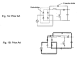
- a prior art boost converter comprising a diode bridge (dashed box) on the input side is shown in fig. 1A .
- the boost converter comprises a protection diode in parallel with the boost inductor and boost diode.
- Fig. 1B shows how a surge current (solid arrows) from the AC input flows through the boost converter and through the protection diodes. The dashed arrows are illustrating how the current would flow without the protection diode.
- the protection diode protects the inductor, switch and boost diode, and only the protection diode needs to be dimensioned for the surge current.
- US 7265650 discloses a PFC circuit comprising a first converter and a second converter and a multi-port electromagnetic device.
- Fig. 25 of the document discloses a boost converter comprising two start-up diodes.
- An AC/DC converter comprising a bridgeless boost converter is also known from " Common mode EMI noise suppression in bridgeless boost PFC convert", Pengju Komng et al, Applied Power Electronics Conference, APEC 2007, IEEE, 1 February 2007 pages 929 - 935 .
- the present invention provides a device arranged for converting an AC input voltage to a DC output voltage comprising a bridgeless boost converter and protection system which provides protection to the boost converter from surges and other unwanted occurrences from the AC mains. Consequently, the protection system will also provide protection to the load or other components on the DC side of the power supply system.
- the object of the invention is also to contribute to increased power efficiency for the power supply system.
- the present invention relates to a device arranged for converting an AC input voltage to a DC output voltage, comprising a bridgeless boost converter; where the device further comprises a surge protection system comprising:
- the AC voltage is normally the AC mains.
- the DC output voltage can be supplied directly to a load or can be supplied to a DC-DC converter for further improving the quality of the DC voltage delivered to a load.
- fig. 2A and 2B illustrating a device with a three-level bridgeless boost converter and a protection system.
- the surge protection system comprises four protection diodes:
- the surge protection system is illustrated by means of a dashed box in fig. 2A .
- a typical bridgeless boost converter comprises:
- protection diodes Dprot1, Dprot2, Dprot3 and Dprot4 are dimensioned to withstand a surge, i.e. a surge current/voltage that is arriving from the AC input, for example because of a lightning that strikes the AC mains net.
- the boost inductor device comprises a first boost inductor Lb1 connected between the first AC input terminal and a first node 1. Moreover, the boost inductor device comprises a second boost inductor Lb2 connected between the second AC input terminal and a second node 2.
- the boost diode device comprises a first boost diode Db1 and a second boost diode Db2.
- the first boost diode Db1 is connected between the first node 1 and the positive boost output terminal Obp.
- the second boost diode Db2 is connected between the negative output terminal Obn and the first node 1. It should be noted that the first boost diode Db1 is connected with its anode to the first node 1 and the second boost diode Db2 is connected with its cathode to the first node 1.
- the boost switch device comprises a first boost switch Sb1 connected to the first node 1 on one end and to a second boost switch Sb2 on the other end.
- the second boost switch Sb2 is connected between the first boost switch Sb1 and the second node 2.
- the boost switches Sb1, Sb2 are connected in series as a so-called bidirectional switch.
- the boost capacitor device comprises a first boost capacitor Cb1 connected between the positive output terminal Obp and the second node 2 and a second boost capacitor Cb2 connected between the second node 2 and the negative output terminal Obn.
- the switches are of type MOSFET switches.
- the switches are switches with intrinsic diodes or switches connected in parallel with anti-parallel diodes.
- An example of alternative switches is IGBTs connected in parallel with anti-parallel diodes.
- the switches are controlled by a control system based on parameters such as measured voltages and/or currents.
- the method used by the control system for controlling the switches would be known for a man skilled in the art.
- the control system can be implemented by means of one or several analogue control circuits or digital signal processors.
Landscapes
- Engineering & Computer Science (AREA)
- Power Engineering (AREA)
- Rectifiers (AREA)
- Dc-Dc Converters (AREA)
- Ac-Ac Conversion (AREA)
- Emergency Protection Circuit Devices (AREA)
Claims (2)
- Vorrichtung zum Umwandeln einer Wechselstrom-Eingangsspannung in eine Gleichstrom-Ausgangsspannung, wobei die Vorrichtung einen brückenlosen Verstärkungswandler aufweist,
wobei die Vorrichtung ferner ein Überspannungsschutzsystem beinhaltet, das Folgendes aufweist:- eine erste Schutzdiode (Dprot1), bei der die Anode mit einem ersten Wechselstrom-Eingangsanschluß des brückenlosen Verstärkungswandlers verbunden ist und die Kathode mit einem positiven Verstärkungsausgangsanschluß (Obp) des brückenlosen Verstärkungswandlers verbunden ist;- eine zweite Schutzdiode (Dprot2), bei der die Anode mit einem negativen Verstärkungsausgangsanschluß (Obn) des brückenlosen Verstärkungswandlers verbunden ist und die Kathode mit dem ersten Wechselstrom-Eingangsanschluß des brückenlosen Verstärkungswandlers verbunden ist;- eine dritte Schutzdiode (Dprot3), bei der die Anode mit einem zweiten Wechselstrom-Eingangsanschluß des brückenlosen Verstärkungswandlers verbunden ist und die Kathode mit dem positiven Verstärkungsausgangsanschluß (Obp) des brückenlosen Verstärkungswandlers verbunden ist;- eine vierte Schutzdiode (Dprot4), bei der die Anode mit dem negativen Verstärkungsausgangsanschluß (Obn) des brückenlosen Verstärkungswandlers verbunden ist und die Kathode mit dem zweiten Wechselstrom-Eingangsanschluß des brückenlosen Verstärkungswandlers verbunden ist;wobei die Schutzdioden (Dprot1, Dprot2, Dprot3, Dprot4) so dimensioniert sind, dass sie einen Strom-/Spannungsstoß aushalten,
wobei der brückenlose Verstärkungswandler Folgendes aufweist:- eine Verstärkungsinduktivitätsvorrichtung, die mindestens eine Verstärkungsinduktivität aufweist;- eine Verstärkungsdiodenvorrichtung, die mindestens eine Verstärkungsdiode aufweist;- eine Verstärkungsschaltervorrichtung, die mindestens einen Verstärkungsschalter aufweist; und- eine Verstärkungskondensatorvorrichtung, die mindestens einen Verstärkungskondensator aufweist,dadurch gekennzeichnet, dass- die Verstärkungsinduktivitätsvorrichtung eine erste Verstärkungsinduktivität (Lb1), die mit einem ersten Ende mit dem ersten Wechselstrom-Eingangsanschluß verbunden ist und mit einem zweiten Ende mit einem ersten Knotenpunkt (1) verbunden ist, sowie eine zweite Verstärkungsinduktivität (Lb2) aufweist, die mit einem ersten Ende mit dem zweiten Wechselstrom-Eingangsanschluß verbunden ist und mit einem zweiten Ende mit einem zweiten Knotenpunkt (2) verbunden ist;- die Verstärkungsdiodenvorrichtung eine erste Verstärkungsdiode (Db1), die zwischen den ersten Knotenpunkt (1) und den positiven Verstärkungsausgangsanschluß (Obp) geschaltet ist, und eine zweite Verstärkungsdiode (Db2) aufweist, die zwischen den negativen Ausgangsanschluß (Obn) und den ersten Knotenpunkt (1) geschaltet ist;- die Verstärkungsschaltervorrichtung einen ersten Verstärkungsschalter (Sb1) und einen zweiten Verstärkungsschalter (Sb2) aufweist, die als bidirektionaler Schalter zwischen dem ersten Knotenpunkt (1) und dem zweiten Knotenpunkt (2) in Reihe geschaltet sind; und- die Verstärkungskondensatorvorrichtung einen ersten Verstärkungskondensator (Cb1), der zwischen den positiven Ausgangsanschluß (Obp) und den zweiten Knotenpunkt (2) geschaltet ist, sowie einen zweiten Verstärkungskondensator (Cb2) aufweist, der zwischen den zweiten Knotenpunkt (2) und den negativen Ausgangsanschluß (Obn) geschaltet ist. - Vorrichtung nach Anspruch 1,
dadurch gekennzeichnet,
dass die erste Verstärkungsdiode (Db1) mit ihrer Anode mit dem ersten Knotenpunkt (1) verbunden ist, und die zweite Verstärkungsdiode (Db2) mit ihrer Kathode mit dem ersten Knotenpunkt (1) verbunden ist.
Priority Applications (2)
| Application Number | Priority Date | Filing Date | Title |
|---|---|---|---|
| SI200830562T SI2215709T1 (sl) | 2007-10-31 | 2008-10-30 | Naprava za pretvorbo vstopne izmenične napetostiv enosmerno izhodno napetost |
| PL08844359T PL2215709T3 (pl) | 2007-10-31 | 2008-10-30 | Urządzenie przystosowane do przetwarzania napięcia przemiennego na napięcie stałe |
Applications Claiming Priority (3)
| Application Number | Priority Date | Filing Date | Title |
|---|---|---|---|
| US98393807P | 2007-10-31 | 2007-10-31 | |
| GB0721413A GB2454216A (en) | 2007-10-31 | 2007-10-31 | Surge protector for a bridgeless boost converter |
| PCT/NO2008/000383 WO2009058024A1 (en) | 2007-10-31 | 2008-10-30 | Device arranged for converting an ac input voltage to a dc output voltage |
Publications (3)
| Publication Number | Publication Date |
|---|---|
| EP2215709A1 EP2215709A1 (de) | 2010-08-11 |
| EP2215709B1 EP2215709B1 (de) | 2012-02-01 |
| EP2215709B2 true EP2215709B2 (de) | 2015-12-09 |
Family
ID=38834630
Family Applications (1)
| Application Number | Title | Priority Date | Filing Date |
|---|---|---|---|
| EP08844359.3A Not-in-force EP2215709B2 (de) | 2007-10-31 | 2008-10-30 | Einrichtung zum umsetzen einer eingangswechselspannung in eine ausgangsgleichspannung |
Country Status (12)
| Country | Link |
|---|---|
| US (1) | US8270129B2 (de) |
| EP (1) | EP2215709B2 (de) |
| CN (1) | CN101919149B (de) |
| AT (1) | ATE544227T1 (de) |
| DK (1) | DK2215709T3 (de) |
| ES (1) | ES2380417T3 (de) |
| GB (1) | GB2454216A (de) |
| HR (1) | HRP20120267T1 (de) |
| PL (1) | PL2215709T3 (de) |
| PT (1) | PT2215709E (de) |
| SI (1) | SI2215709T1 (de) |
| WO (1) | WO2009058024A1 (de) |
Families Citing this family (32)
| Publication number | Priority date | Publication date | Assignee | Title |
|---|---|---|---|---|
| CN101645649B (zh) * | 2008-08-07 | 2012-11-14 | 艾默生网络能源系统北美公司 | 一种防浪涌pfc电路 |
| US8508166B2 (en) | 2009-08-10 | 2013-08-13 | Emerson Climate Technologies, Inc. | Power factor correction with variable bus voltage |
| US8358098B2 (en) * | 2009-08-10 | 2013-01-22 | Emerson Climate Technologies, Inc. | System and method for power factor correction |
| US8264192B2 (en) | 2009-08-10 | 2012-09-11 | Emerson Climate Technologies, Inc. | Controller and method for transitioning between control angles |
| EP2309639B1 (de) * | 2009-10-09 | 2016-02-10 | SMA Solar Technology AG | Blindleistungsfähiger Wechselrichter |
| FR2953663B1 (fr) * | 2009-12-03 | 2012-02-03 | Aeg Power Solutions Bv | Circuit de pre-charge pour convertisseur ac/dc |
| CN101841236A (zh) * | 2010-04-22 | 2010-09-22 | 华为技术有限公司 | 一种功率因数矫正变换器及其控制方法 |
| KR101195903B1 (ko) | 2010-10-29 | 2012-11-01 | 세빈기술주식회사 | 멀티 채널 무선 데이터 송수신 모듈 및 이를 이용한 메쉬망 중계 방법 |
| CN102751861A (zh) * | 2011-04-21 | 2012-10-24 | 艾默生网络能源系统北美公司 | 一种无桥功率因数校正电路 |
| WO2012106862A1 (zh) * | 2011-07-01 | 2012-08-16 | 华为技术有限公司 | 功率因数校正转换器以及功率因数校正转换设备 |
| US8385032B1 (en) | 2011-08-23 | 2013-02-26 | Futurewei Technologies, Inc. | High efficiency bridgeless PFC converter and method |
| US9590495B2 (en) * | 2011-08-26 | 2017-03-07 | Futurewei Technologies, Inc. | Holdup time circuit and method for bridgeless PFC converter |
| GB2501104A (en) | 2012-04-12 | 2013-10-16 | Eltek As | Compact, efficient common mode inductor for a power converter system |
| GB2501106A (en) | 2012-04-12 | 2013-10-16 | Eltek As | Power supply system with a power converter unit and a rack |
| GB2501105A (en) | 2012-04-12 | 2013-10-16 | Eltek As | AC-DC converter overvoltage protection circuit |
| GB2501108B (en) | 2012-04-12 | 2014-10-22 | Eltek As | DC-DC converter device |
| US9634593B2 (en) | 2012-04-26 | 2017-04-25 | Emerson Climate Technologies, Inc. | System and method for permanent magnet motor control |
| WO2014026124A1 (en) | 2012-08-10 | 2014-02-13 | Emerson Climate Technologies, Inc. | Motor drive control using pulse-width modulation pulse skipping |
| CN103812315A (zh) * | 2012-11-12 | 2014-05-21 | 中兴通讯股份有限公司 | 一种浪涌保护电路 |
| US9323267B2 (en) | 2013-03-14 | 2016-04-26 | Flextronics Ap, Llc | Method and implementation for eliminating random pulse during power up of digital signal controller |
| US9494658B2 (en) | 2013-03-14 | 2016-11-15 | Flextronics Ap, Llc | Approach for generation of power failure warning signal to maximize useable hold-up time with AC/DC rectifiers |
| US9490651B2 (en) | 2013-03-15 | 2016-11-08 | Flextronics Ap, Llc | Sweep frequency mode for magnetic resonant power transmission |
| US9899910B2 (en) * | 2013-05-30 | 2018-02-20 | Flextronics Ap, Llc | Bridgeless PFC power converter with reduced EMI noise |
| US9621053B1 (en) | 2014-08-05 | 2017-04-11 | Flextronics Ap, Llc | Peak power control technique for primary side controller operation in continuous conduction mode |
| EP3001553A1 (de) * | 2014-09-25 | 2016-03-30 | ABB Oy | Elektrische Anordnung |
| CN104467390A (zh) * | 2014-11-26 | 2015-03-25 | 无锡上能新能源有限公司 | 一种换流器保护电路及包括该电路的换流器 |
| CA2983171C (en) * | 2015-04-20 | 2018-12-04 | Toshiba Mitsubishi-Electric Industrial Systems Corporation | Converter and power conversion device including the same |
| CN104883052B (zh) * | 2015-06-07 | 2017-11-14 | 上海华虹宏力半导体制造有限公司 | 提升电容电路以及电荷泵 |
| CN106026630A (zh) * | 2016-05-18 | 2016-10-12 | 浙江大学 | 一种变模态无桥pfc电路 |
| CN111181377B (zh) * | 2020-01-07 | 2021-04-30 | 茂硕电源科技股份有限公司 | 一种功率因数校正电路 |
| CN113497550B (zh) * | 2021-06-21 | 2022-06-03 | 成都天通电子科技有限公司 | 一种ac-dc电源开机浪涌电流的控制电路 |
| KR20230032758A (ko) | 2021-08-31 | 2023-03-07 | 삼성전자주식회사 | 전자 장치 및 그 제어 방법 |
Family Cites Families (8)
| Publication number | Priority date | Publication date | Assignee | Title |
|---|---|---|---|---|
| DE3907193C2 (de) | 1988-03-11 | 1998-08-20 | Honda Motor Co Ltd | Fahrgeschwindigkeitsregler für ein Kraftfahrzeug |
| FI81701C (fi) * | 1988-05-17 | 1990-11-12 | Kone Oy | Oeverspaenningsskydd foer riktarbryggor. |
| US5088019A (en) * | 1990-09-18 | 1992-02-11 | Hewlett-Packard Company | Low harmonic current and fault tolerant power supply |
| DE9216662U1 (de) * | 1992-12-07 | 1993-01-28 | Siemens AG, 80333 München | Vorladeschaltung mit kombiniertem Überspannungsschutz für einen netzgeführten Stromrichter mit ausgangsseitigem Kondensator |
| US6088209A (en) * | 1998-11-19 | 2000-07-11 | Power Paragon, Inc. | Voltage spike suppressor |
| JP4096656B2 (ja) | 2002-08-02 | 2008-06-04 | 富士電機機器制御株式会社 | 整流装置 |
| US7164591B2 (en) * | 2003-10-01 | 2007-01-16 | International Rectifier Corporation | Bridge-less boost (BLB) power factor correction topology controlled with one cycle control |
| US7355868B2 (en) | 2005-03-31 | 2008-04-08 | International Rectifier Corporation | Current sense method for bridgeless boost (BLB) PFC circuit using single current transformer |
-
2007
- 2007-10-31 GB GB0721413A patent/GB2454216A/en not_active Withdrawn
-
2008
- 2008-10-30 HR HR20120267T patent/HRP20120267T1/hr unknown
- 2008-10-30 PL PL08844359T patent/PL2215709T3/pl unknown
- 2008-10-30 WO PCT/NO2008/000383 patent/WO2009058024A1/en not_active Ceased
- 2008-10-30 SI SI200830562T patent/SI2215709T1/sl unknown
- 2008-10-30 ES ES08844359T patent/ES2380417T3/es active Active
- 2008-10-30 CN CN200880124162.9A patent/CN101919149B/zh active Active
- 2008-10-30 US US12/740,652 patent/US8270129B2/en active Active
- 2008-10-30 DK DK08844359.3T patent/DK2215709T3/da active
- 2008-10-30 PT PT08844359T patent/PT2215709E/pt unknown
- 2008-10-30 AT AT08844359T patent/ATE544227T1/de active
- 2008-10-30 EP EP08844359.3A patent/EP2215709B2/de not_active Not-in-force
Also Published As
| Publication number | Publication date |
|---|---|
| PL2215709T3 (pl) | 2012-07-31 |
| EP2215709B1 (de) | 2012-02-01 |
| US8270129B2 (en) | 2012-09-18 |
| HRP20120267T1 (hr) | 2012-04-30 |
| SI2215709T1 (sl) | 2012-05-31 |
| ATE544227T1 (de) | 2012-02-15 |
| EP2215709A1 (de) | 2010-08-11 |
| DK2215709T3 (da) | 2012-05-21 |
| CN101919149B (zh) | 2014-01-08 |
| CN101919149A (zh) | 2010-12-15 |
| GB2454216A (en) | 2009-05-06 |
| GB0721413D0 (en) | 2007-12-12 |
| PT2215709E (pt) | 2012-04-10 |
| ES2380417T3 (es) | 2012-05-11 |
| US20100277837A1 (en) | 2010-11-04 |
| WO2009058024A1 (en) | 2009-05-07 |
Similar Documents
| Publication | Publication Date | Title |
|---|---|---|
| EP2215709B2 (de) | Einrichtung zum umsetzen einer eingangswechselspannung in eine ausgangsgleichspannung | |
| US8736238B2 (en) | Buck and buck/boost converter systems having auxiliary circuits and method thereof | |
| Tofoli et al. | Novel nonisolated high-voltage gain dc–dc converters based on 3SSC and VMC | |
| US11451135B2 (en) | Multilevel port under-voltage protection circuit with flying capacitor | |
| US20120268084A1 (en) | Bridgeless power factor correction circuit | |
| EP2218169B1 (de) | Wechselstrom-gleichstrom-aufwärtswandler ohne brücke | |
| US6169671B1 (en) | Snubber circuit for a power switch and recitifying diode and power converter employing the same | |
| CN103081320A (zh) | 高效电力调节器和方法 | |
| CN111416528B (zh) | 功率转换器和控制功率转换器的方法 | |
| US20150357906A1 (en) | Converter | |
| CN115580121A (zh) | 防雷击保护的电源供应器 | |
| Hoch et al. | Voltage multiplier applied to boost DC–DC converter: analysis, design, and performance evaluations | |
| CN210380245U (zh) | 直流耗能系统及电力系统 | |
| CN103187721A (zh) | 包括过电压保护功能的电源装置 | |
| US20090257247A1 (en) | Switching Power Supply Circuit and Surge Absobring Circuit | |
| KR20150044335A (ko) | 전원 공급 장치 및 방법 | |
| US11456660B2 (en) | Grounding scheme for power conversion system | |
| WO2008155600A1 (en) | Improved switched-mode power converter and method | |
| KR101734215B1 (ko) | 안정성이 향상된 양방향 비절연 dc-dc 컨버터 | |
| Qiu et al. | An AC VRM topology for high frequency AC power distribution systems | |
| EP4123893A1 (de) | Aktiver gleichrichter in einem schaltnetzteil | |
| KR100834031B1 (ko) | 스너버회로를 이용한 역률개선회로 | |
| CN219513968U (zh) | 一种电源电路及电源适配器 | |
| CN113691119B (zh) | 三相功率因素校正装置 | |
| EP4387399B1 (de) | Überspannungsschutzschaltung und stromversorgung zum betrieb aus einem gleichstromnetz |
Legal Events
| Date | Code | Title | Description |
|---|---|---|---|
| PUAI | Public reference made under article 153(3) epc to a published international application that has entered the european phase |
Free format text: ORIGINAL CODE: 0009012 |
|
| 17P | Request for examination filed |
Effective date: 20100531 |
|
| AK | Designated contracting states |
Kind code of ref document: A1 Designated state(s): AT BE BG CH CY CZ DE DK EE ES FI FR GB GR HR HU IE IS IT LI LT LU LV MC MT NL NO PL PT RO SE SI SK TR |
|
| AX | Request for extension of the european patent |
Extension state: AL BA MK RS |
|
| DAX | Request for extension of the european patent (deleted) | ||
| GRAP | Despatch of communication of intention to grant a patent |
Free format text: ORIGINAL CODE: EPIDOSNIGR1 |
|
| GRAS | Grant fee paid |
Free format text: ORIGINAL CODE: EPIDOSNIGR3 |
|
| GRAA | (expected) grant |
Free format text: ORIGINAL CODE: 0009210 |
|
| AK | Designated contracting states |
Kind code of ref document: B1 Designated state(s): AT BE BG CH CY CZ DE DK EE ES FI FR GB GR HR HU IE IS IT LI LT LU LV MC MT NL NO PL PT RO SE SI SK TR |
|
| REG | Reference to a national code |
Ref country code: GB Ref legal event code: FG4D |
|
| REG | Reference to a national code |
Ref country code: CH Ref legal event code: EP Ref country code: AT Ref legal event code: REF Ref document number: 544227 Country of ref document: AT Kind code of ref document: T Effective date: 20120215 |
|
| REG | Reference to a national code |
Ref country code: NL Ref legal event code: T3 |
|
| REG | Reference to a national code |
Ref country code: HR Ref legal event code: TUEP Ref document number: P20120267 Country of ref document: HR |
|
| REG | Reference to a national code |
Ref country code: DE Ref legal event code: R096 Ref document number: 602008013145 Country of ref document: DE Effective date: 20120329 |
|
| REG | Reference to a national code |
Ref country code: SE Ref legal event code: TRGR |
|
| REG | Reference to a national code |
Ref country code: RO Ref legal event code: EPE |
|
| REG | Reference to a national code |
Ref country code: PT Ref legal event code: SC4A Free format text: AVAILABILITY OF NATIONAL TRANSLATION Effective date: 20120326 |
|
| REG | Reference to a national code |
Ref country code: HR Ref legal event code: T1PR Ref document number: P20120267 Country of ref document: HR |
|
| REG | Reference to a national code |
Ref country code: ES Ref legal event code: FG2A Ref document number: 2380417 Country of ref document: ES Kind code of ref document: T3 Effective date: 20120511 |
|
| REG | Reference to a national code |
Ref country code: DK Ref legal event code: T3 |
|
| REG | Reference to a national code |
Ref country code: NO Ref legal event code: T2 Effective date: 20120201 |
|
| REG | Reference to a national code |
Ref country code: GR Ref legal event code: EP Ref document number: 20120400933 Country of ref document: GR Effective date: 20120518 |
|
| REG | Reference to a national code |
Ref country code: SK Ref legal event code: T3 Ref document number: E 11498 Country of ref document: SK |
|
| LTIE | Lt: invalidation of european patent or patent extension |
Effective date: 20120201 |
|
| PG25 | Lapsed in a contracting state [announced via postgrant information from national office to epo] |
Ref country code: LT Free format text: LAPSE BECAUSE OF FAILURE TO SUBMIT A TRANSLATION OF THE DESCRIPTION OR TO PAY THE FEE WITHIN THE PRESCRIBED TIME-LIMIT Effective date: 20120201 Ref country code: IS Free format text: LAPSE BECAUSE OF FAILURE TO SUBMIT A TRANSLATION OF THE DESCRIPTION OR TO PAY THE FEE WITHIN THE PRESCRIBED TIME-LIMIT Effective date: 20120601 |
|
| REG | Reference to a national code |
Ref country code: PL Ref legal event code: T3 |
|
| REG | Reference to a national code |
Ref country code: EE Ref legal event code: FG4A Ref document number: E006814 Country of ref document: EE Effective date: 20120502 |
|
| PG25 | Lapsed in a contracting state [announced via postgrant information from national office to epo] |
Ref country code: LV Free format text: LAPSE BECAUSE OF FAILURE TO SUBMIT A TRANSLATION OF THE DESCRIPTION OR TO PAY THE FEE WITHIN THE PRESCRIBED TIME-LIMIT Effective date: 20120201 |
|
| REG | Reference to a national code |
Ref country code: HR Ref legal event code: ODRP Ref document number: P20120267 Country of ref document: HR Payment date: 20120926 Year of fee payment: 5 |
|
| PG25 | Lapsed in a contracting state [announced via postgrant information from national office to epo] |
Ref country code: CY Free format text: LAPSE BECAUSE OF FAILURE TO SUBMIT A TRANSLATION OF THE DESCRIPTION OR TO PAY THE FEE WITHIN THE PRESCRIBED TIME-LIMIT Effective date: 20120201 |
|
| REG | Reference to a national code |
Ref country code: HU Ref legal event code: AG4A Ref document number: E013860 Country of ref document: HU |
|
| PLBI | Opposition filed |
Free format text: ORIGINAL CODE: 0009260 |
|
| PGFP | Annual fee paid to national office [announced via postgrant information from national office to epo] |
Ref country code: RO Payment date: 20120927 Year of fee payment: 5 |
|
| 26 | Opposition filed |
Opponent name: AEG POWER SOLUTIONS B.V. Effective date: 20121016 |
|
| PGFP | Annual fee paid to national office [announced via postgrant information from national office to epo] |
Ref country code: PL Payment date: 20120926 Year of fee payment: 5 Ref country code: LU Payment date: 20121023 Year of fee payment: 5 Ref country code: HR Payment date: 20120926 Year of fee payment: 5 |
|
| PLAX | Notice of opposition and request to file observation + time limit sent |
Free format text: ORIGINAL CODE: EPIDOSNOBS2 |
|
| PGFP | Annual fee paid to national office [announced via postgrant information from national office to epo] |
Ref country code: DK Payment date: 20121022 Year of fee payment: 5 |
|
| REG | Reference to a national code |
Ref country code: DE Ref legal event code: R026 Ref document number: 602008013145 Country of ref document: DE Effective date: 20121016 |
|
| PGFP | Annual fee paid to national office [announced via postgrant information from national office to epo] |
Ref country code: FI Payment date: 20121011 Year of fee payment: 5 Ref country code: EE Payment date: 20121011 Year of fee payment: 5 Ref country code: CZ Payment date: 20121024 Year of fee payment: 5 Ref country code: CH Payment date: 20121023 Year of fee payment: 5 Ref country code: BG Payment date: 20121011 Year of fee payment: 5 Ref country code: BE Payment date: 20121022 Year of fee payment: 5 Ref country code: HU Payment date: 20121029 Year of fee payment: 5 Ref country code: MC Payment date: 20121011 Year of fee payment: 5 Ref country code: IE Payment date: 20121019 Year of fee payment: 5 |
|
| PGFP | Annual fee paid to national office [announced via postgrant information from national office to epo] |
Ref country code: SI Payment date: 20120924 Year of fee payment: 5 Ref country code: TR Payment date: 20121001 Year of fee payment: 5 Ref country code: ES Payment date: 20121026 Year of fee payment: 5 Ref country code: GR Payment date: 20121030 Year of fee payment: 5 Ref country code: PT Payment date: 20120326 Year of fee payment: 5 Ref country code: SE Payment date: 20121019 Year of fee payment: 5 Ref country code: IT Payment date: 20121023 Year of fee payment: 5 Ref country code: SK Payment date: 20121029 Year of fee payment: 5 |
|
| PGFP | Annual fee paid to national office [announced via postgrant information from national office to epo] |
Ref country code: NL Payment date: 20121019 Year of fee payment: 5 |
|
| PLBB | Reply of patent proprietor to notice(s) of opposition received |
Free format text: ORIGINAL CODE: EPIDOSNOBS3 |
|
| PG25 | Lapsed in a contracting state [announced via postgrant information from national office to epo] |
Ref country code: MT Free format text: LAPSE BECAUSE OF FAILURE TO SUBMIT A TRANSLATION OF THE DESCRIPTION OR TO PAY THE FEE WITHIN THE PRESCRIBED TIME-LIMIT Effective date: 20120201 |
|
| BERE | Be: lapsed |
Owner name: ELTEK VALERE AS Effective date: 20131031 |
|
| REG | Reference to a national code |
Ref country code: PT Ref legal event code: MM4A Free format text: LAPSE DUE TO NON-PAYMENT OF FEES Effective date: 20140430 |
|
| REG | Reference to a national code |
Ref country code: HR Ref legal event code: PBON Ref document number: P20120267 Country of ref document: HR Effective date: 20131030 |
|
| REG | Reference to a national code |
Ref country code: NL Ref legal event code: V1 Effective date: 20140501 |
|
| REG | Reference to a national code |
Ref country code: DK Ref legal event code: EBP Effective date: 20131031 |
|
| PG25 | Lapsed in a contracting state [announced via postgrant information from national office to epo] |
Ref country code: MC Free format text: LAPSE BECAUSE OF NON-PAYMENT OF DUE FEES Effective date: 20131031 |
|
| REG | Reference to a national code |
Ref country code: CH Ref legal event code: PL |
|
| REG | Reference to a national code |
Ref country code: SE Ref legal event code: EUG |
|
| TPAC | Observations filed by third parties |
Free format text: ORIGINAL CODE: EPIDOSNTIPA |
|
| REG | Reference to a national code |
Ref country code: EE Ref legal event code: MM4A Ref document number: E006814 Country of ref document: EE Effective date: 20131031 |
|
| REG | Reference to a national code |
Ref country code: GR Ref legal event code: ML Ref document number: 20120400933 Country of ref document: GR Effective date: 20140505 |
|
| REG | Reference to a national code |
Ref country code: SK Ref legal event code: MM4A Ref document number: E 11498 Country of ref document: SK Effective date: 20131030 |
|
| REG | Reference to a national code |
Ref country code: IE Ref legal event code: MM4A |
|
| PG25 | Lapsed in a contracting state [announced via postgrant information from national office to epo] |
Ref country code: EE Free format text: LAPSE BECAUSE OF NON-PAYMENT OF DUE FEES Effective date: 20131031 Ref country code: CH Free format text: LAPSE BECAUSE OF NON-PAYMENT OF DUE FEES Effective date: 20131031 Ref country code: LI Free format text: LAPSE BECAUSE OF NON-PAYMENT OF DUE FEES Effective date: 20131031 |
|
| REG | Reference to a national code |
Ref country code: SI Ref legal event code: KO00 Effective date: 20140620 |
|
| PG25 | Lapsed in a contracting state [announced via postgrant information from national office to epo] |
Ref country code: CZ Free format text: LAPSE BECAUSE OF NON-PAYMENT OF DUE FEES Effective date: 20131030 Ref country code: FI Free format text: LAPSE BECAUSE OF NON-PAYMENT OF DUE FEES Effective date: 20131030 Ref country code: SI Free format text: LAPSE BECAUSE OF NON-PAYMENT OF DUE FEES Effective date: 20131031 Ref country code: NL Free format text: LAPSE BECAUSE OF NON-PAYMENT OF DUE FEES Effective date: 20140501 Ref country code: IT Free format text: LAPSE BECAUSE OF NON-PAYMENT OF DUE FEES Effective date: 20131030 Ref country code: SE Free format text: LAPSE BECAUSE OF NON-PAYMENT OF DUE FEES Effective date: 20131031 Ref country code: SK Free format text: LAPSE BECAUSE OF NON-PAYMENT OF DUE FEES Effective date: 20131030 Ref country code: PT Free format text: LAPSE BECAUSE OF NON-PAYMENT OF DUE FEES Effective date: 20140430 Ref country code: RO Free format text: LAPSE BECAUSE OF NON-PAYMENT OF DUE FEES Effective date: 20131030 |
|
| PG25 | Lapsed in a contracting state [announced via postgrant information from national office to epo] |
Ref country code: HU Free format text: LAPSE BECAUSE OF NON-PAYMENT OF DUE FEES Effective date: 20131031 Ref country code: BE Free format text: LAPSE BECAUSE OF NON-PAYMENT OF DUE FEES Effective date: 20131031 Ref country code: HR Free format text: LAPSE BECAUSE OF NON-PAYMENT OF DUE FEES Effective date: 20131030 |
|
| PG25 | Lapsed in a contracting state [announced via postgrant information from national office to epo] |
Ref country code: IE Free format text: LAPSE BECAUSE OF NON-PAYMENT OF DUE FEES Effective date: 20131030 Ref country code: DK Free format text: LAPSE BECAUSE OF NON-PAYMENT OF DUE FEES Effective date: 20131031 |
|
| REG | Reference to a national code |
Ref country code: ES Ref legal event code: FD2A Effective date: 20141107 |
|
| REG | Reference to a national code |
Ref country code: AT Ref legal event code: MM01 Ref document number: 544227 Country of ref document: AT Kind code of ref document: T Effective date: 20131030 |
|
| PG25 | Lapsed in a contracting state [announced via postgrant information from national office to epo] |
Ref country code: ES Free format text: LAPSE BECAUSE OF NON-PAYMENT OF DUE FEES Effective date: 20131031 |
|
| REG | Reference to a national code |
Ref country code: PL Ref legal event code: LAPE |
|
| PG25 | Lapsed in a contracting state [announced via postgrant information from national office to epo] |
Ref country code: AT Free format text: LAPSE BECAUSE OF NON-PAYMENT OF DUE FEES Effective date: 20131030 Ref country code: PL Free format text: LAPSE BECAUSE OF NON-PAYMENT OF DUE FEES Effective date: 20131030 |
|
| PG25 | Lapsed in a contracting state [announced via postgrant information from national office to epo] |
Ref country code: LU Free format text: LAPSE BECAUSE OF NON-PAYMENT OF DUE FEES Effective date: 20131030 Ref country code: BG Free format text: LAPSE BECAUSE OF NON-PAYMENT OF DUE FEES Effective date: 20131031 |
|
| PG25 | Lapsed in a contracting state [announced via postgrant information from national office to epo] |
Ref country code: TR Free format text: LAPSE BECAUSE OF NON-PAYMENT OF DUE FEES Effective date: 20131030 |
|
| REG | Reference to a national code |
Ref country code: FR Ref legal event code: PLFP Year of fee payment: 8 |
|
| PUAH | Patent maintained in amended form |
Free format text: ORIGINAL CODE: 0009272 |
|
| STAA | Information on the status of an ep patent application or granted ep patent |
Free format text: STATUS: PATENT MAINTAINED AS AMENDED |
|
| 27A | Patent maintained in amended form |
Effective date: 20151209 |
|
| AK | Designated contracting states |
Kind code of ref document: B2 Designated state(s): AT BE BG CH CY CZ DE DK EE ES FI FR GB GR HR HU IE IS IT LI LT LU LV MC MT NL NO PL PT RO SE SI SK TR |
|
| REG | Reference to a national code |
Ref country code: DE Ref legal event code: R102 Ref document number: 602008013145 Country of ref document: DE |
|
| REG | Reference to a national code |
Ref country code: NO Ref legal event code: TB2 |
|
| PG25 | Lapsed in a contracting state [announced via postgrant information from national office to epo] |
Ref country code: GR Free format text: LAPSE BECAUSE OF FAILURE TO SUBMIT A TRANSLATION OF THE DESCRIPTION OR TO PAY THE FEE WITHIN THE PRESCRIBED TIME-LIMIT Effective date: 20160310 |
|
| PG25 | Lapsed in a contracting state [announced via postgrant information from national office to epo] |
Ref country code: GR Free format text: LAPSE BECAUSE OF FAILURE TO SUBMIT A TRANSLATION OF THE DESCRIPTION OR TO PAY THE FEE WITHIN THE PRESCRIBED TIME-LIMIT Effective date: 20140505 |
|
| REG | Reference to a national code |
Ref country code: FR Ref legal event code: PLFP Year of fee payment: 9 |
|
| REG | Reference to a national code |
Ref country code: FR Ref legal event code: PLFP Year of fee payment: 10 |
|
| REG | Reference to a national code |
Ref country code: FR Ref legal event code: PLFP Year of fee payment: 11 |
|
| PG25 | Lapsed in a contracting state [announced via postgrant information from national office to epo] |
Ref country code: BG Free format text: LAPSE BECAUSE OF NON-PAYMENT OF DUE FEES Effective date: 20170808 |
|
| PGFP | Annual fee paid to national office [announced via postgrant information from national office to epo] |
Ref country code: FR Payment date: 20191219 Year of fee payment: 13 |
|
| PGFP | Annual fee paid to national office [announced via postgrant information from national office to epo] |
Ref country code: NO Payment date: 20200817 Year of fee payment: 13 |
|
| PGFP | Annual fee paid to national office [announced via postgrant information from national office to epo] |
Ref country code: GB Payment date: 20201022 Year of fee payment: 13 Ref country code: DE Payment date: 20201022 Year of fee payment: 13 |
|
| REG | Reference to a national code |
Ref country code: DE Ref legal event code: R119 Ref document number: 602008013145 Country of ref document: DE |
|
| REG | Reference to a national code |
Ref country code: NO Ref legal event code: MMEP |
|
| GBPC | Gb: european patent ceased through non-payment of renewal fee |
Effective date: 20211030 |
|
| PG25 | Lapsed in a contracting state [announced via postgrant information from national office to epo] |
Ref country code: NO Free format text: LAPSE BECAUSE OF NON-PAYMENT OF DUE FEES Effective date: 20211031 Ref country code: GB Free format text: LAPSE BECAUSE OF NON-PAYMENT OF DUE FEES Effective date: 20211030 Ref country code: DE Free format text: LAPSE BECAUSE OF NON-PAYMENT OF DUE FEES Effective date: 20220503 |
|
| PG25 | Lapsed in a contracting state [announced via postgrant information from national office to epo] |
Ref country code: FR Free format text: LAPSE BECAUSE OF NON-PAYMENT OF DUE FEES Effective date: 20211031 |