EP4387399B1 - Überspannungsschutzschaltung und stromversorgung zum betrieb aus einem gleichstromnetz - Google Patents
Überspannungsschutzschaltung und stromversorgung zum betrieb aus einem gleichstromnetz Download PDFInfo
- Publication number
- EP4387399B1 EP4387399B1 EP22213166.6A EP22213166A EP4387399B1 EP 4387399 B1 EP4387399 B1 EP 4387399B1 EP 22213166 A EP22213166 A EP 22213166A EP 4387399 B1 EP4387399 B1 EP 4387399B1
- Authority
- EP
- European Patent Office
- Prior art keywords
- circuit
- voltage
- surge protection
- grid
- protection circuit
- Prior art date
- Legal status (The legal status is an assumption and is not a legal conclusion. Google has not performed a legal analysis and makes no representation as to the accuracy of the status listed.)
- Active
Links
Images
Classifications
-
- H—ELECTRICITY
- H05—ELECTRIC TECHNIQUES NOT OTHERWISE PROVIDED FOR
- H05B—ELECTRIC HEATING; ELECTRIC LIGHT SOURCES NOT OTHERWISE PROVIDED FOR; CIRCUIT ARRANGEMENTS FOR ELECTRIC LIGHT SOURCES, IN GENERAL
- H05B47/00—Circuit arrangements for operating light sources in general, i.e. where the type of light source is not relevant
- H05B47/20—Responsive to malfunctions or to light source life; for protection
- H05B47/24—Circuit arrangements for protecting against overvoltage
Definitions
- the mains supply may have the form of a 400 V/50Hz AC mains supply.
- a DC grid operating with a nominal 565 V DC nominal voltage may enable to integrate energy storage devices, renewable energy sources and a plurality of different industrial devices including, for example stationary robotic devices and machining centres of manufacturing cells, or elements of the building infrastructure, e.g. lifts, lighting or heating and ventilation systems.
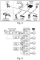
- Figs. 4 and 5 of the attached figure sheets illustrate potential layouts for future industrial applications.
- DC grids operating at high nominal DC voltages e.g. in voltage ranges between 400 V DC and 800 V DC , and, in particular, the cited 565 V DC voltage level for a passive rectification, or a 650 V DC voltage level for an active rectification with a power factor correction (PFC) may become the predominant or even exclusive source of electric energy at the manufacturing site.
- PFC power factor correction
- these further building infrastructure systems are increasingly required to rely DC-to-DC converter devices operating from the DC grid in order to generate and provide a DC load current to their respective electric load, e.g. to lighting modules.
- US 2017/311400 A1 discloses a load control device for controlling power delivered from a power source to an electrical load
- the load control device comprises a control circuit configured to control the load regulation circuit to control the power delivered to the electrical load.
- the control circuit is configured to operate in an AC mode when an input voltage is an AC voltage and in a DC mode when the input voltage is a DC voltage.
- the control circuit is configured to disable the power converter in the DC mode.
- the control circuit is configured to render a controllable switching circuit conductive in the AC mode, and non-conductive in the DC mode.
- the rectifier circuit is configured to rectify the input voltage to generate a rectified voltage when the input voltage is an AC voltage, and to pass through the input voltage when the input voltage is a DC voltage.
- US 2019/335552 A1 discloses a power circuit.
- DC-to-DC converters e.g. LED drivers
- DC-to-DC converters e.g. LED drivers
- Current DC-to-DC converters use electronic components such as capacitors and semiconductors, e.g. MOSFETs, rated for voltages up to 650 V DC, which are sufficient to cope with the overvoltages, which may be encountered at the power supply interfaces of the current DC-to-DC converters to the current AC grid operating at nominal voltages of 400 V AC , for example. This situation changes for the power supply interface with the DC grid at a nominal voltage of 565 V DC or even 800 V DC . Voltage surges with voltages of, e.g. 1500 V DC may occur.
- the diode effectively protects the at least one transistor from a drop in the voltage provided by the DC grid to the DC-to-DC converter device. Integrating renewable energy sources directly onto the DC grid, for example, may result in sudden voltage drops in the DC voltage provided by the DC grid to the DC-to-DC converter device. Without the diode, the transistor will most probably suffer destruction due to voltage drop.
- the DC grid voltage may, for example, correspond to a DC voltage between 400 V DC and 800 400 V DC .
- Fig. 1 further shows a DC output interface of the electronic circuit 10 to an electrical load 15.
- the electrical load 15 may be a lighting module (LED module) including a plurality of light emitting diodes (LEDs), which the electronic circuit 10 provides with a bus voltage V BUS via a bus bar.
- the lighting module shown in fig. 1 also includes a DC-to-DC converter 15.1, which generates a LED current I LED as a particular example for the load current I LOAD , and provides the LED current I LED to the LEDs.
- the DC-to-DC converter 15.1 may generate the load current I LOAD based on the bus voltage V BUS using a switched mode power supply (SMPS) topology. Arranging the DC-to-DC converter 15.1 in the electrical load 15, e.g. the lighting module, enables to use different electrical loads 15 connected to the same bus bar with the bus voltage V BUS .
- SMPS switched mode power supply
- the electronic circuit 10 includes an optional driver circuit 12 that generates the bus voltage V BUS from a voltage V 2 input to the optional driver circuit 12.
- the optional driver circuit 12 is not limited to a particular SMPS configuration.
- the electronic circuit 10 arranges the EMI filter circuit 11 connected, in particular directly connected, to the positive supply line connection L of the DC grid interface on the one hand and to an input (first input line, first input connection) of the surge protection circuit 1.
- Electromagnetic interference is a disruption that affects an electrical circuit because of either electromagnetic induction or externally emitted electromagnetic radiation.
- EMI refers to the interference from one electrical or electronic system to another electronic system caused by electromagnetic fields generated by the operation of the electronic system.
- EMI also refers to a disturbance generated by an external source that affects an electrical circuit by electromagnetic induction, electrostatic coupling, or electric conduction. The disturbance may degrade the performance of the electric circuit or even prevent the electric circuit from functioning entirely.
- the EMI filter circuit 11 blocks disturbances as near to the source as possible, preferably, before the disturbances enter the electronic circuit or before the disturbance leave the electronic circuit.
- Examples of the EMI filter circuit 11 arranged on a circuit board of the electronic circuit use respectively arranged capacitors and/or inductors.
- An EMI choke as an example of the EMI filter circuit 11 of fig. 1 shows an equivalent circuit diagram including an inductivity L2 serially connected with a resistor R2, and a capacitor C2 connected in parallel to the serially arranged inductivity L2 and resistor R2.
- the EMI filter circuit 11 provides a reactive impedance to the electronic circuit 10, and, by determining the electric component values of the EMI filter circuit 11 respectively, a frequency characteristics of the EMI filter circuit 11 may be tuned to desired frequency ranges.
- a line filter is an example for an EMI filter circuit 11.
- the line filter is an electronic filter circuit that is placed between electronic equipment and a line (power supply line, power supply connection) external to it, to attenuate conducted radio frequencies in this context as Radiated Frequency Interference (abbreviated as RFI, sometimes also referenced under to term electromagnetic interference EMI) - between the line and the electronic equipment.
- RFI Radiated Frequency Interference
- EMI electromagnetic interference
- an AC line filter is used between the AC power line (AC power supply connection) and the equipment, e.g. a SMPS or a similar electronic circuit.
- the line filter may be used to attenuate EMI in either direction of the power supply connection.
- the line filter may be used to reduce the level of EMI entering the equipment, to a level sufficiently low not to cause any undesired behaviour.
- a first functional element of the surge protection circuit 1 is a serial circuit element 2 connected between the output of the EMI filter circuit 11 connected with the first input connection of the surge protection circuit 1 and the terminal N of the DC grid interface.
- the serial circuit element 2 is configured to implement a low-pass filter.
- the first functional element 2 of the surge protection circuit 1 corresponds to a low-pass filter, comprising the R-C element including at least one resistor that corresponds to the resistor R7, connected in series with a filter load of the low-pass filter and at least one capacitor that corresponds to the capacitor C5 connected in parallel with the filter load of the low-pass filter.
- the average DC voltage from the DC supply grid of nominally 650 V, and up to 800 V, or for example down to 400 V provided via the DC grid interface of the DC-to- electronic circuit 10, may apply.
- a simple low-pass filter circuit may comprise the resistor R7 in series with a load to the low-pass filter, and the capacitor C5 in parallel with the load of the low-pass filter.
- the capacitor C5 acts as a reactance, and blocks low-frequency signal components, forcing them through the filter towards the load of the low-pass filter instead.
- the reactance drops, and the capacitor C5 effectively functions as a short circuit.
- the combination of resistor R7 and capacitor C5 connected in series determines a time constant of the low-pass filter.
- Determining the capacitance value of C7 may have to take into regard that a duration of the attenuation of voltage surges is a desired effect of the determined capacitance value of C7.
- selecting the capacitance value of C7 to large may adversely affect the voltages V IN1 , V IN2 and V BUS .
- V IN1 , V IN2 and V BUS may show voltage drops in cases, in which the capacitance of C7 shows large capacitance values and the size of the load 15 varies significantly, in particular, sudden load steps occur.
- the at least one transistor Q1, Q2 may be in connected in an emitter-follower circuit topology.
- a collector of the at least one transistor Q1, Q2 is connected with the first input connection of the surge protection circuit 1.
- An emitter of the at least one transistor Q1, Q2 is connected with a first output connection (first output line) of the surge protection circuit 1.
- a base of the at least one transistor Q1, Q2 is connected with the second connection of the resistor R7 and the first connection of the capacitor C5.
- An emitter-follower also referred as a common collector amplifier is one of three basic single-stage bipolar junction transistor (abbreviated as BJT) amplifier topologies, typically used as a voltage buffer.
- BJT bipolar junction transistor
- the emitter-follower circuit topology uses the base terminal of the transistor as input, the emitter corresponds to an output, and the collector is common to both the emitter and the collector, e.g., it may be tied to ground reference or a power supply rail.
- the surge protection circuit 1 may comprise a first transistor Q1 and at least one second transistor Q2 instead of a single transistor, wherein the first transistor Q1 and the at least one second transistor Q2 are connected in a Darlington configuration.
- a Darlington configuration refers to an electronic circuit topology including at least two transistors. Also called a Darlington pair, the Darlington configuration or circuit topology is an electronic circuit comprising two bipolar transistors with the emitter of a second transistor Q2 of the two transistors Q1, Q2 connected to the base of the first transistor Q1 of the two transistors Q1, Q2. The first transistor Q1 amplifies a current amplified by the second transistor Q2 further. In the Darlington configuration, the collectors of both transistors Q1, Q2 are connected with each other. The Darlington configuration has a significantly higher current gain than each transistor of the two transistors Q1, Q2 taken separately.
- the surge protection circuit 1 may use the two transistors Q1, Q2 in a Darlington configuration in order to provide sufficient current gain in application scenarios, in which one transistor with sufficient current gain is not available.
- a voltage drop between the emitter of the transistor Q2, and the emitter of the transistor Q1 may correspond to about 0.7 V.
- the linear regulator circuit element 3 implemented using the transistors Q1, Q2 of the surge protection circuit 1 passes a voltage V IN2 corresponding to the DC grid voltage to the optional driver circuit 12.
- the surge protection circuit 1 may provide the voltage V IN2 directly to the bus bar. Then the voltage V IN2 essentially corresponds to a bus voltage V BUS .
- the transistors Q1, Q2 may be Metal Oxide Semiconductor Field Effect Transistors (MOSFETs), for example.
- MOSFETs Metal Oxide Semiconductor Field Effect Transistors
- the analogous field-effect transistor circuit topology to the Darlington configuration is the common-drain amplifier circuit topology.
- the surge protection circuit 1 may arrange a diode D7 as a further functional element of the surge protection circuit 1 between an emitter of the first transistor Q1, which is connected to the output connection of the surge protection circuit 1, and the base of the second transistor Q2.
- an anode of the diode D7 is connected with the emitter of the first transistor Q1, and a cathode of the diode D7 is connected with the base of the second transistor Q2 in case the surge protection circuit 1 includes two transistors Q1, Q2 in a Darlington configuration according to fig. 1.
- the anode of the diode D7 is connected with the emitter of the transistor Q1, and a cathode of the diode D7 is connected with a base of the transistor Q1 in case the surge protection circuit includes only a single transistor Q1, different from the embodiment illustrated in fig. 1.
- the diode D7 provides the effect of protecting the transistors Q1, Q2 in case the DC grid voltage V DC , and in consequence the voltages V IN2 and V IN2 drop significantly, e.g. to values down to 400 V, for example due to stability problems in the DC supply grid originating from an integration of renewable energy sources into the DC grid.
- the output of the surge protection circuit 1 is connected, in particular directly connected with the input of the optional driver circuit 12.
- the output of the surge protection circuit 1 is directly connected, to the bus interface of the electronic circuit 10.
- the presence of the surge protection circuit 1, has the effect that short voltage surges in the DC grid are now admissible. Characteristically, voltage surges are defined for up to 1200 V peak for a duration of up to 100 ⁇ s in the DC supply grid.
- the low-pass filter implemented by the first functional element of the surge protection circuit 1 is designed to filter these defined voltage surges out.
- a voltage applied over capacitor C5 remains at the nominal voltage of 650 V, the first transistor Q1 blocks the overvoltage, e.g. the 1200 V less 650 V, at the expense of a small power loss. The power loss is small, as the first transistor Q1 does not entirely block the voltage, but only for a duration of 100 ⁇ s of the voltage surge.
- the surge protection circuit 1 may cope with the additional power dissipation due to a corresponding dynamic heat resistance.
- a junction temperature of transistors Q1, Q2 does not increase immediately with the power loss due to the voltage surge.
- Fig. 2 displays a simplified circuit diagram of a known DC-to-DC converter device 21 from prior art including surge protection as currently in use.
- the DC-to-DC converter device 21 includes most functional elements of the electronic circuit 10 discussed with reference to fig. 1. In particular, with respect to the EMI filter circuit 22 and the converter circuit 24, reference to the corresponding EMI filter circuit 11 is considered sufficient.
- the converter circuit 24 may be a known DC-to-DC converter circuit implemented in a switched mode power supply topology.
- the converter circuit 24 generates a load current I LOAD .
- the DC-to-DC converter device 21 employs a conventional surge protection means 23.
- the surge protection means 23 comprises a voltage-dependent resistor, which fig. 2 shows with an equivalent circuit including the elements ideal capacitor C4, ideal resistor R5 and ideal inductivity L5 in a series connection.
- the surge protection means 23 is connected from a positive polarity DC supply line (positive polarity DC supply connection) to a negative polarity DC supply line (negative polarity DC supply connection) at the DC grid interface of the DC-to-DC converter device 21 in order to protect the electric components of the converter circuit 24 from overvoltage.
- VDR Voltage Dependent Resistors
- MOV metal oxide varistor
- NTC Negative Temperature Coefficient
- a thermistor is a type of resistor whose resistance is strongly dependent on temperature, more so than in standard resistors. Thermistors are divided based on their conduction model. NTC thermistor are widely used as inrush current limiters, temperature sensors, while PTC thermistors are used as self-resetting overcurrent protectors, and self-regulating heating elements. An operational temperature range of a thermistor is dependent on the probe type and may typically be between -100 °C and 300 °C.
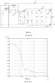
- Fig. 3 illustrates the reaction of the known DC-to-DC converter device 21 with surge protection as currently in use in a hot replacement scenario.
- the electrical device when an electrical device is turned on, the electrical device may draw a current significantly larger than a nominal current during standard operation of the electrical device.
- the large current drawn for s short time after applying a DC voltage step to the electrical device is referenced an inrush current, sometimes also denoted as input surge current or switch-on surge.
- the inrush current is the maximal instantaneous input current drawn by the electrical device when applying a voltage step to the input of a power supply interface of the electrical device.
- Alternating-current electric motors and transformers may draw several times their nominal current under full-load conditions when first energized, for a few cycles of the input waveform.
- the electronic circuit 1 includes the surge protection circuit 1, which is capable to suppress the voltage surge of the bus voltage V BUS shown in fig. 3 entirely.
- the surge protection circuit 1 does not only provide protection of the optional driver circuit 12 against voltage surges of the DC grid but also provides the extra benefit of addressing the problems arising from the inrush current scenario.
- Fig. 4 displays a simplified structure of an industrial DC grid and its key elements.
- the DC grid also enables integrating energy storage devices at the manufacturing site with the benefit of reduced conversion losses. This provides the additional effect of maintaining electric power supply for the manufacturing site in case of an AC grid failure. Thus, a peak power requirement when designing the AC grid over a region with a plurality of manufacturing sites, and the bidirectional power supply for the individual manufacturing site, may be reduced.
- a high ratio of recuperative energy may be used locally at the manufacturing site, or fed to the AC grid.
- the DC grid for a manufacturing site enables seamless and efficient integration of renewable energy, e.g. solar panels installed on factory roofs, and storage devices for balancing power supply and demand in the factory.
- Fig. 4 shows a direct current supply of an entire manufacturing facility extending a direct current supply of a production cell, which provides the groundwork for the power supply of manufacturing plants via a DC grid.
- the DC grid enables to implement an energy transition in industrial production achieving a significant reduction of consumed power and a recovery of braking energy.
- Robotic devices in manufacturing plants may recuperate energy and store recuperated energy into the energy storage devices at the DC voltage level of the DC grid.
- a LED driver uses cheap semiconductors, e.g. 650V-rated MOSFETs.
- Use of electronic components extending the rated voltages of the electronic components up to 900 V is envisaged, but already comes at the expense of increased cost.
- Fig. 5 illustrates the simplified structure of an industrial DC grid stabilizing energy availability in future industrial applications.
- the implementation of the DC grid at manufacturing sites has the potential to reduce operating costs and take advantage of renewable energy sources. Conversion from DC to AC is not required to be done by an inverter - the grid infrastructure provided by the DC grid offers the possibility of optimizing the purchase of energy and to stabilize the grid.
- a frequency inverter is supplied with the alternating current, which is first converted into direct current using a rectifier. The direct current is then converted into alternating current with variable frequency and voltage through a voltage feed inverter in order to electronically change the speed of a three-phase motor.
- the energy flow changes. This energy cannot be fed back into the grid by the frequency inverter because the input rectifier only allows the energy to flow in one direction. Therefore, the energy that is fed back must be dissipated via the direct current voltage circuit of the frequency inverter.
- frequency inverters to control motor speeds causes effects on mains supply, causing harmonics and distorting the voltage of the mains supply grid. If frequency inverters or other devices with power electronics are increasingly installed, grid effects such as harmonics and voltage surges on a mains supply grid will increase.
- a further increase in the use of inverters for the flexible control of electric motors is desirable in order to improve both production processes and energy efficiency.
- line perturbations due to harmonics and equipment costs e.g. for other systems operating of the mains supply grid at the manufacturing site limit the improvement.
- the network structure of the mains supply grid at the manufacturing site according to fig. 5 is based on an alternating current (AC) supply, which provides the direct current power supply for the manufacturing site via a central rectifier.
- Active grid filters may be integrated into the central rectifier to ensure the voltage quality harmonic requirements.
- the direct supply of the frequency inverter with direct current means that a decentralized energy conversion is no longer needed. Since central energy conversion from AC to DC is significantly more efficient, conversion losses are significantly reduced.
- the DC grid offers the possibility of integrating photovoltaics directly at the direct current voltage level. In this case, conversion from DC to AC is not required to be done by an inverter.
- This grid infrastructure offers the possibility of optimizing purchase of energy, and stabilizing the grid.
- the electronic circuit 10 with the surge protection circuit 1 enables to integrate building infrastructure systems, e.g. lighting systems, into the DC grid at the manufacturing site.
Landscapes
- Emergency Protection Circuit Devices (AREA)
Claims (12)
- Elektronische Schaltung einschließlich einer Überspannungsschutzschaltung (1) für die Leistungsversorgungsschnittstelle einer Gleichstromumrichtervorrichtung (10), wobei die elektronische Schaltung eine Gleichstrom-Netzschnittstelle umfasst, umfassend eine erste und eine zweite Gleichstromeingangsspannungsleitung (L, N), und
wobei die Überspannungsschutzschaltung (1) umfasst:ein serielles Schaltungselement (2), das zwischen die erste und die zweite Gleichstromeingangsspannungsleitung (L, N) geschaltet ist und konfiguriert ist, um einen Tiefpassfilter zu implementieren, undein lineares Reglerschaltungselement (3), einschließlich mindestens eines Transistors (Q1, Q2), unddadurch gekennzeichnet, dassdie Überspannungsschutzschaltung (1) das serielle Schaltungselement (2) umfasst, umfassend ein RC-Element zum Implementieren des Tiefpassfilters einschließlich mindestens eines Widerstands (R7) und eines Kondensator (C5),wobei ein erster Anschluss des mindestens einen Widerstands (R7) mit der ersten Gleichspannungseingangsleitung (L) geschaltet ist und ein zweiter Anschluss des mindestens einen Widerstands (R7) mit einem ersten Anschluss des Kondensators (C5) geschaltet ist und ein zweiter Anschluss des Kondensators (C5) mit der zweiten Gleichspannungseingangsleitung (N) geschaltet ist, undwobei eine Basis des mindestens einen Transistors (Q1, Q2) mit dem zweiten Anschluss des mindestens einen Widerstands (R7) und dem ersten Anschluss des Kondensators (C5) geschaltet ist und ein Emitter des mindestens einen Transistors (Q1, Q2) mit einem Ausgangsanschluss der Überspannungsschutzschaltung (1) geschaltet ist. - Elektronische Schaltung einschließlich der Überspannungsschutzschaltung (1) für eine Gleichstromumrichtervorrichtung nach Anspruch 1, wobei
die Überspannungsschutzschaltung (1) mindestens einen Transistor (Q1, Q2) des linearen Reglerschaltungselements (3) in einer Emitterfolger-Schaltungstopologiekonfiguration umfasst. - Elektronische Schaltung einschließlich der Überspannungsschutzschaltung (1) für eine Gleichstromumrichtervorrichtung nach einem der vorstehenden Ansprüche, wobei
die Überspannungsschutzschaltung (1) ferner eine Diode (D7) umfasst, die zwischen einem Emitter des mindestens einen Transistors (Q1, Q2) und einer Basis des mindestens einen Transistors (Q1, Q2) geschaltet ist. - Elektronische Schaltung einschließlich der Überspannungsschutzschaltung (1) für eine Gleichstromumrichtervorrichtung nach einem der vorstehenden Ansprüche, wobei
die Überspannungsschutzschaltung (1) den ersten Transistor (Q1) und mindestens einen zweiten Transistor (Q2) umfasst, wobei der erste Transistor (Q1) und der mindestens eine zweite Transistor (Q2) in einer Darlington-Konfiguration geschaltet sind. - Elektronische Schaltung einschließlich der Überspannungsschutzschaltung (1) für eine Gleichstromumrichtervorrichtung nach einem der vorstehenden Ansprüche, wobei
die Überspannungsschutzschaltung (1) konfiguriert ist, um in einem Spannungsbereich einer Gleichstromnetzversorgung betrieben zu werden. - Elektronische Schaltung einschließlich der Überspannungsschutzschaltung (1) für eine Gleichstromumrichtervorrichtung nach Anspruch 5, wobei
die Überspannungsschutzschaltung (1) konfiguriert ist, um in einem Nennspannungsbereich der Gleichstromnetzversorgung, die in dem Bereich von 400 VDC bis 950 VDC liegt, betrieben zu werden. - Elektronische Schaltung einschließlich der Überspannungsschutzschaltung (1) für eine Gleichstromumrichtervorrichtung nach Anspruch 5 oder 6, wobei
die Nennspannung der Gleichstromnetzversorgung im Wesentlichen 650 V entspricht. - Leistungsversorgung zum Erzeugen eines Laststroms (ILOAD) für eine elektrische Last (15) aus einer Gleichstromversorgungsspannung, wobei die Leistungsversorgung umfasst:eine Gleichstromumrichterschaltung (15.1), die konfiguriert ist, um den Laststrom (ILOAD) zu erzeugen und den Laststrom (ILOAD) über eine Ausgangsschnittstelle (LED+, LED-) auszugeben, undwobei die elektronische Schaltung die Überspannungsschutzschaltung (1) nach einem der Ansprüche 1 bis 7 einschließt und konfiguriert ist, um zwischen die Gleichstromnetzschnittstelle zum Erhalten der Gleichstromversorgungsspannung und die Gleichstromumrichterschaltung (15.1) geschaltet zu werden.
- Leistungsversorgung nach Anspruch 8, wobei
die Gleichstromumrichterschaltung (15.1) elektrische Komponenten mit einem Spannungsnennwert einschließt, der eine Nennspannung der Gleichstromnetzversorgungsspannung überschreitet und kleiner als eine maximale Spitzenspannung der Gleichstromnetzversorgungsspannung ist. - Leistungsversorgung nach Anspruch 9, wobei der Spannungsnennwert die Nennspannung der Gleichstromnetzversorgungsspannung übersteigt und kleiner als das Zweifache der Nennspannung der Gleichstromnetzversorgungsspannung ist, oder
der Spannungsnennwert 800 V überschreitet und kleiner als oder gleich 950 V ist. - Leistungsversorgung nach einem der Ansprüche 8 bis 10, wobeidie Leistungsversorgung eine EMI-Filterschaltung (11) umfasst, unddie EMI-Filterschaltung (11) zwischen der Gleichstromnetzschnittstelle und der Überspannungsschutzschaltung (1) angeschlossen ist.
- Leistungsversorgung nach einem der Ansprüche 8 bis 11, wobei
die Leistungsversorgung ein Lichttreiber ist, der konfiguriert ist, um den Laststrom (ILOAD) zum Versorgen mindestens eines Beleuchtungsmoduls bereitzustellen.
Priority Applications (2)
| Application Number | Priority Date | Filing Date | Title |
|---|---|---|---|
| EP22213166.6A EP4387399B1 (de) | 2022-12-13 | 2022-12-13 | Überspannungsschutzschaltung und stromversorgung zum betrieb aus einem gleichstromnetz |
| PCT/EP2023/084260 WO2024126157A1 (en) | 2022-12-13 | 2023-12-05 | Surge protection circuit and power supply for operating from a dc grid |
Applications Claiming Priority (1)
| Application Number | Priority Date | Filing Date | Title |
|---|---|---|---|
| EP22213166.6A EP4387399B1 (de) | 2022-12-13 | 2022-12-13 | Überspannungsschutzschaltung und stromversorgung zum betrieb aus einem gleichstromnetz |
Publications (2)
| Publication Number | Publication Date |
|---|---|
| EP4387399A1 EP4387399A1 (de) | 2024-06-19 |
| EP4387399B1 true EP4387399B1 (de) | 2025-07-02 |
Family
ID=84519432
Family Applications (1)
| Application Number | Title | Priority Date | Filing Date |
|---|---|---|---|
| EP22213166.6A Active EP4387399B1 (de) | 2022-12-13 | 2022-12-13 | Überspannungsschutzschaltung und stromversorgung zum betrieb aus einem gleichstromnetz |
Country Status (2)
| Country | Link |
|---|---|
| EP (1) | EP4387399B1 (de) |
| WO (1) | WO2024126157A1 (de) |
Family Cites Families (5)
| Publication number | Priority date | Publication date | Assignee | Title |
|---|---|---|---|---|
| GB2491550A (en) * | 2011-01-17 | 2012-12-12 | Radiant Res Ltd | A hybrid power control system using dynamic power regulation to increase the dimming dynamic range and power control of solid-state illumination systems |
| US9113521B2 (en) * | 2013-05-29 | 2015-08-18 | Lutron Electronics Co., Inc. | Load control device for a light-emitting diode light source |
| WO2016145264A1 (en) * | 2015-03-10 | 2016-09-15 | Innosys, Inc. | Solid state fluorescent lamp and high intensity discharge replacement |
| EP3449695B1 (de) * | 2016-04-25 | 2025-07-02 | Lutron Technology Company LLC | Laststeuerungsvorrichtung für eine leuchtdiodenlichtquelle |
| US10645767B2 (en) * | 2018-04-26 | 2020-05-05 | Qatar University | Linear regulated dimmable LED driver for DC distributed lighting system |
-
2022
- 2022-12-13 EP EP22213166.6A patent/EP4387399B1/de active Active
-
2023
- 2023-12-05 WO PCT/EP2023/084260 patent/WO2024126157A1/en not_active Ceased
Also Published As
| Publication number | Publication date |
|---|---|
| EP4387399A1 (de) | 2024-06-19 |
| WO2024126157A1 (en) | 2024-06-20 |
Similar Documents
| Publication | Publication Date | Title |
|---|---|---|
| CN109417353B (zh) | 用于直流电源应用的调压变压整流组件 | |
| US7253537B2 (en) | System and method of operating double fed induction generators | |
| US8068324B2 (en) | Circuit and method for protecting energy-storage device | |
| EP2999075B1 (de) | Stromversorgung mit Überspannungsableiterschutz | |
| US9735725B2 (en) | Methods and systems for transient voltage protection | |
| US7804271B2 (en) | Multiphase current supplying circuit, driving apparatus, compressor and air conditioner | |
| US7471011B2 (en) | Wind turbine over-voltage exposure | |
| CN111224374B (zh) | 一种保护电路 | |
| JP7182719B2 (ja) | 駆動制御回路、エアコン及びコントローラ | |
| US20160164273A1 (en) | Over-voltage protection apparatus and method of operating the same | |
| US8670253B2 (en) | Converter protecting components against overvoltages | |
| CN105680793B (zh) | 一种光伏系统的电压补偿装置及光伏系统 | |
| CN101350516B (zh) | 保护储能装置的电路及方法 | |
| CN210380245U (zh) | 直流耗能系统及电力系统 | |
| EP4387399B1 (de) | Überspannungsschutzschaltung und stromversorgung zum betrieb aus einem gleichstromnetz | |
| JP2001238465A (ja) | インバータ装置 | |
| CN219740030U (zh) | 车载冗余电源和电动汽车 | |
| US20180342943A1 (en) | Grounding scheme for power conversion system | |
| JP2007221844A (ja) | マトリクスコンバータ装置及びその保護装置 | |
| US20200044560A1 (en) | Power Supply Circuit | |
| US6577485B2 (en) | Ultra-wide input range power supply for circuit protection devices | |
| KR101409355B1 (ko) | 고압 배전선로용 전원 공급 장치 | |
| CN217159542U (zh) | 一种空调变频控制器的抗共模浪涌电压冲击电路 | |
| KR101792540B1 (ko) | Mmc 컨버터의 서브모듈용 전원제어장치 | |
| US7199987B2 (en) | Diode system having zener diodes and a generator |
Legal Events
| Date | Code | Title | Description |
|---|---|---|---|
| PUAI | Public reference made under article 153(3) epc to a published international application that has entered the european phase |
Free format text: ORIGINAL CODE: 0009012 |
|
| STAA | Information on the status of an ep patent application or granted ep patent |
Free format text: STATUS: THE APPLICATION HAS BEEN PUBLISHED |
|
| AK | Designated contracting states |
Kind code of ref document: A1 Designated state(s): AL AT BE BG CH CY CZ DE DK EE ES FI FR GB GR HR HU IE IS IT LI LT LU LV MC ME MK MT NL NO PL PT RO RS SE SI SK SM TR |
|
| STAA | Information on the status of an ep patent application or granted ep patent |
Free format text: STATUS: REQUEST FOR EXAMINATION WAS MADE |
|
| 17P | Request for examination filed |
Effective date: 20241014 |
|
| RBV | Designated contracting states (corrected) |
Designated state(s): AL AT BE BG CH CY CZ DE DK EE ES FI FR GB GR HR HU IE IS IT LI LT LU LV MC ME MK MT NL NO PL PT RO RS SE SI SK SM TR |
|
| GRAP | Despatch of communication of intention to grant a patent |
Free format text: ORIGINAL CODE: EPIDOSNIGR1 |
|
| STAA | Information on the status of an ep patent application or granted ep patent |
Free format text: STATUS: GRANT OF PATENT IS INTENDED |
|
| INTG | Intention to grant announced |
Effective date: 20250228 |
|
| GRAS | Grant fee paid |
Free format text: ORIGINAL CODE: EPIDOSNIGR3 |
|
| GRAA | (expected) grant |
Free format text: ORIGINAL CODE: 0009210 |
|
| STAA | Information on the status of an ep patent application or granted ep patent |
Free format text: STATUS: THE PATENT HAS BEEN GRANTED |
|
| P01 | Opt-out of the competence of the unified patent court (upc) registered |
Free format text: CASE NUMBER: APP_21124/2025 Effective date: 20250505 |
|
| AK | Designated contracting states |
Kind code of ref document: B1 Designated state(s): AL AT BE BG CH CY CZ DE DK EE ES FI FR GB GR HR HU IE IS IT LI LT LU LV MC ME MK MT NL NO PL PT RO RS SE SI SK SM TR |
|
| REG | Reference to a national code |
Ref country code: GB Ref legal event code: FG4D |
|
| REG | Reference to a national code |
Ref country code: CH Ref legal event code: EP |
|
| REG | Reference to a national code |
Ref country code: DE Ref legal event code: R096 Ref document number: 602022016825 Country of ref document: DE |
|
| REG | Reference to a national code |
Ref country code: IE Ref legal event code: FG4D |
|
| REG | Reference to a national code |
Ref country code: DE Ref legal event code: R084 Ref document number: 602022016825 Country of ref document: DE |
|
| REG | Reference to a national code |
Ref country code: NL Ref legal event code: MP Effective date: 20250702 |
|
| PG25 | Lapsed in a contracting state [announced via postgrant information from national office to epo] |
Ref country code: PT Free format text: LAPSE BECAUSE OF FAILURE TO SUBMIT A TRANSLATION OF THE DESCRIPTION OR TO PAY THE FEE WITHIN THE PRESCRIBED TIME-LIMIT Effective date: 20251103 |
|
| PG25 | Lapsed in a contracting state [announced via postgrant information from national office to epo] |
Ref country code: NL Free format text: LAPSE BECAUSE OF FAILURE TO SUBMIT A TRANSLATION OF THE DESCRIPTION OR TO PAY THE FEE WITHIN THE PRESCRIBED TIME-LIMIT Effective date: 20250702 |
|
| REG | Reference to a national code |
Ref country code: AT Ref legal event code: MK05 Ref document number: 1810820 Country of ref document: AT Kind code of ref document: T Effective date: 20250702 |
|
| PG25 | Lapsed in a contracting state [announced via postgrant information from national office to epo] |
Ref country code: IS Free format text: LAPSE BECAUSE OF FAILURE TO SUBMIT A TRANSLATION OF THE DESCRIPTION OR TO PAY THE FEE WITHIN THE PRESCRIBED TIME-LIMIT Effective date: 20251102 |
|
| PG25 | Lapsed in a contracting state [announced via postgrant information from national office to epo] |
Ref country code: NO Free format text: LAPSE BECAUSE OF FAILURE TO SUBMIT A TRANSLATION OF THE DESCRIPTION OR TO PAY THE FEE WITHIN THE PRESCRIBED TIME-LIMIT Effective date: 20251002 |
|
| REG | Reference to a national code |
Ref country code: LT Ref legal event code: MG9D |
|
| PG25 | Lapsed in a contracting state [announced via postgrant information from national office to epo] |
Ref country code: AT Free format text: LAPSE BECAUSE OF FAILURE TO SUBMIT A TRANSLATION OF THE DESCRIPTION OR TO PAY THE FEE WITHIN THE PRESCRIBED TIME-LIMIT Effective date: 20250702 |
|
| PG25 | Lapsed in a contracting state [announced via postgrant information from national office to epo] |
Ref country code: FI Free format text: LAPSE BECAUSE OF FAILURE TO SUBMIT A TRANSLATION OF THE DESCRIPTION OR TO PAY THE FEE WITHIN THE PRESCRIBED TIME-LIMIT Effective date: 20250702 |
|
| PG25 | Lapsed in a contracting state [announced via postgrant information from national office to epo] |
Ref country code: HR Free format text: LAPSE BECAUSE OF FAILURE TO SUBMIT A TRANSLATION OF THE DESCRIPTION OR TO PAY THE FEE WITHIN THE PRESCRIBED TIME-LIMIT Effective date: 20250702 |
|
| PGFP | Annual fee paid to national office [announced via postgrant information from national office to epo] |
Ref country code: FR Payment date: 20251223 Year of fee payment: 4 |
|
| PG25 | Lapsed in a contracting state [announced via postgrant information from national office to epo] |
Ref country code: GR Free format text: LAPSE BECAUSE OF FAILURE TO SUBMIT A TRANSLATION OF THE DESCRIPTION OR TO PAY THE FEE WITHIN THE PRESCRIBED TIME-LIMIT Effective date: 20251003 |
|
| PG25 | Lapsed in a contracting state [announced via postgrant information from national office to epo] |
Ref country code: CZ Free format text: LAPSE BECAUSE OF FAILURE TO SUBMIT A TRANSLATION OF THE DESCRIPTION OR TO PAY THE FEE WITHIN THE PRESCRIBED TIME-LIMIT Effective date: 20250702 Ref country code: SE Free format text: LAPSE BECAUSE OF FAILURE TO SUBMIT A TRANSLATION OF THE DESCRIPTION OR TO PAY THE FEE WITHIN THE PRESCRIBED TIME-LIMIT Effective date: 20250702 |
|
| PG25 | Lapsed in a contracting state [announced via postgrant information from national office to epo] |
Ref country code: LV Free format text: LAPSE BECAUSE OF FAILURE TO SUBMIT A TRANSLATION OF THE DESCRIPTION OR TO PAY THE FEE WITHIN THE PRESCRIBED TIME-LIMIT Effective date: 20250702 |
|
| PG25 | Lapsed in a contracting state [announced via postgrant information from national office to epo] |
Ref country code: BG Free format text: LAPSE BECAUSE OF FAILURE TO SUBMIT A TRANSLATION OF THE DESCRIPTION OR TO PAY THE FEE WITHIN THE PRESCRIBED TIME-LIMIT Effective date: 20250702 Ref country code: PL Free format text: LAPSE BECAUSE OF FAILURE TO SUBMIT A TRANSLATION OF THE DESCRIPTION OR TO PAY THE FEE WITHIN THE PRESCRIBED TIME-LIMIT Effective date: 20250702 |
|
| PG25 | Lapsed in a contracting state [announced via postgrant information from national office to epo] |
Ref country code: RS Free format text: LAPSE BECAUSE OF FAILURE TO SUBMIT A TRANSLATION OF THE DESCRIPTION OR TO PAY THE FEE WITHIN THE PRESCRIBED TIME-LIMIT Effective date: 20251002 |
|
| PG25 | Lapsed in a contracting state [announced via postgrant information from national office to epo] |
Ref country code: ES Free format text: LAPSE BECAUSE OF FAILURE TO SUBMIT A TRANSLATION OF THE DESCRIPTION OR TO PAY THE FEE WITHIN THE PRESCRIBED TIME-LIMIT Effective date: 20250702 |
|
| PG25 | Lapsed in a contracting state [announced via postgrant information from national office to epo] |
Ref country code: RO Free format text: LAPSE BECAUSE OF FAILURE TO SUBMIT A TRANSLATION OF THE DESCRIPTION OR TO PAY THE FEE WITHIN THE PRESCRIBED TIME-LIMIT Effective date: 20250702 |
|
| PG25 | Lapsed in a contracting state [announced via postgrant information from national office to epo] |
Ref country code: SM Free format text: LAPSE BECAUSE OF FAILURE TO SUBMIT A TRANSLATION OF THE DESCRIPTION OR TO PAY THE FEE WITHIN THE PRESCRIBED TIME-LIMIT Effective date: 20250702 |
|
| PG25 | Lapsed in a contracting state [announced via postgrant information from national office to epo] |
Ref country code: DK Free format text: LAPSE BECAUSE OF FAILURE TO SUBMIT A TRANSLATION OF THE DESCRIPTION OR TO PAY THE FEE WITHIN THE PRESCRIBED TIME-LIMIT Effective date: 20250702 |
|
| PGFP | Annual fee paid to national office [announced via postgrant information from national office to epo] |
Ref country code: DE Payment date: 20251229 Year of fee payment: 4 |
|
| PG25 | Lapsed in a contracting state [announced via postgrant information from national office to epo] |
Ref country code: IT Free format text: LAPSE BECAUSE OF FAILURE TO SUBMIT A TRANSLATION OF THE DESCRIPTION OR TO PAY THE FEE WITHIN THE PRESCRIBED TIME-LIMIT Effective date: 20250702 |