EP3449695B1 - Laststeuerungsvorrichtung für eine leuchtdiodenlichtquelle - Google Patents
Laststeuerungsvorrichtung für eine leuchtdiodenlichtquelle Download PDFInfo
- Publication number
- EP3449695B1 EP3449695B1 EP17722939.0A EP17722939A EP3449695B1 EP 3449695 B1 EP3449695 B1 EP 3449695B1 EP 17722939 A EP17722939 A EP 17722939A EP 3449695 B1 EP3449695 B1 EP 3449695B1
- Authority
- EP
- European Patent Office
- Prior art keywords
- voltage
- circuit
- load
- bus
- control device
- Prior art date
- Legal status (The legal status is an assumption and is not a legal conclusion. Google has not performed a legal analysis and makes no representation as to the accuracy of the status listed.)
- Active
Links
Images


Classifications
-
- H—ELECTRICITY
- H05—ELECTRIC TECHNIQUES NOT OTHERWISE PROVIDED FOR
- H05B—ELECTRIC HEATING; ELECTRIC LIGHT SOURCES NOT OTHERWISE PROVIDED FOR; CIRCUIT ARRANGEMENTS FOR ELECTRIC LIGHT SOURCES, IN GENERAL
- H05B45/00—Circuit arrangements for operating light-emitting diodes [LED]
- H05B45/40—Details of LED load circuits
- H05B45/44—Details of LED load circuits with an active control inside an LED matrix
-
- H—ELECTRICITY
- H02—GENERATION; CONVERSION OR DISTRIBUTION OF ELECTRIC POWER
- H02M—APPARATUS FOR CONVERSION BETWEEN AC AND AC, BETWEEN AC AND DC, OR BETWEEN DC AND DC, AND FOR USE WITH MAINS OR SIMILAR POWER SUPPLY SYSTEMS; CONVERSION OF DC OR AC INPUT POWER INTO SURGE OUTPUT POWER; CONTROL OR REGULATION THEREOF
- H02M1/00—Details of apparatus for conversion
- H02M1/10—Arrangements incorporating converting means for enabling loads to be operated at will from different kinds of power supplies, e.g. from AC or DC
-
- H—ELECTRICITY
- H05—ELECTRIC TECHNIQUES NOT OTHERWISE PROVIDED FOR
- H05B—ELECTRIC HEATING; ELECTRIC LIGHT SOURCES NOT OTHERWISE PROVIDED FOR; CIRCUIT ARRANGEMENTS FOR ELECTRIC LIGHT SOURCES, IN GENERAL
- H05B45/00—Circuit arrangements for operating light-emitting diodes [LED]
- H05B45/30—Driver circuits
- H05B45/37—Converter circuits
- H05B45/3725—Switched mode power supply [SMPS]
- H05B45/38—Switched mode power supply [SMPS] using boost topology
-
- H—ELECTRICITY
- H05—ELECTRIC TECHNIQUES NOT OTHERWISE PROVIDED FOR
- H05B—ELECTRIC HEATING; ELECTRIC LIGHT SOURCES NOT OTHERWISE PROVIDED FOR; CIRCUIT ARRANGEMENTS FOR ELECTRIC LIGHT SOURCES, IN GENERAL
- H05B45/00—Circuit arrangements for operating light-emitting diodes [LED]
- H05B45/30—Driver circuits
- H05B45/37—Converter circuits
- H05B45/3725—Switched mode power supply [SMPS]
- H05B45/382—Switched mode power supply [SMPS] with galvanic isolation between input and output
-
- H—ELECTRICITY
- H05—ELECTRIC TECHNIQUES NOT OTHERWISE PROVIDED FOR
- H05B—ELECTRIC HEATING; ELECTRIC LIGHT SOURCES NOT OTHERWISE PROVIDED FOR; CIRCUIT ARRANGEMENTS FOR ELECTRIC LIGHT SOURCES, IN GENERAL
- H05B45/00—Circuit arrangements for operating light-emitting diodes [LED]
- H05B45/10—Controlling the intensity of the light
-
- H—ELECTRICITY
- H05—ELECTRIC TECHNIQUES NOT OTHERWISE PROVIDED FOR
- H05B—ELECTRIC HEATING; ELECTRIC LIGHT SOURCES NOT OTHERWISE PROVIDED FOR; CIRCUIT ARRANGEMENTS FOR ELECTRIC LIGHT SOURCES, IN GENERAL
- H05B45/00—Circuit arrangements for operating light-emitting diodes [LED]
- H05B45/30—Driver circuits
- H05B45/37—Converter circuits
- H05B45/3725—Switched mode power supply [SMPS]
- H05B45/39—Circuits containing inverter bridges
-
- H—ELECTRICITY
- H05—ELECTRIC TECHNIQUES NOT OTHERWISE PROVIDED FOR
- H05B—ELECTRIC HEATING; ELECTRIC LIGHT SOURCES NOT OTHERWISE PROVIDED FOR; CIRCUIT ARRANGEMENTS FOR ELECTRIC LIGHT SOURCES, IN GENERAL
- H05B47/00—Circuit arrangements for operating light sources in general, i.e. where the type of light source is not relevant
- H05B47/10—Controlling the light source
- H05B47/155—Coordinated control of two or more light sources
-
- H—ELECTRICITY
- H05—ELECTRIC TECHNIQUES NOT OTHERWISE PROVIDED FOR
- H05B—ELECTRIC HEATING; ELECTRIC LIGHT SOURCES NOT OTHERWISE PROVIDED FOR; CIRCUIT ARRANGEMENTS FOR ELECTRIC LIGHT SOURCES, IN GENERAL
- H05B47/00—Circuit arrangements for operating light sources in general, i.e. where the type of light source is not relevant
- H05B47/10—Controlling the light source
- H05B47/165—Controlling the light source following a pre-assigned programmed sequence; Logic control [LC]
-
- Y—GENERAL TAGGING OF NEW TECHNOLOGICAL DEVELOPMENTS; GENERAL TAGGING OF CROSS-SECTIONAL TECHNOLOGIES SPANNING OVER SEVERAL SECTIONS OF THE IPC; TECHNICAL SUBJECTS COVERED BY FORMER USPC CROSS-REFERENCE ART COLLECTIONS [XRACs] AND DIGESTS
- Y02—TECHNOLOGIES OR APPLICATIONS FOR MITIGATION OR ADAPTATION AGAINST CLIMATE CHANGE
- Y02B—CLIMATE CHANGE MITIGATION TECHNOLOGIES RELATED TO BUILDINGS, e.g. HOUSING, HOUSE APPLIANCES OR RELATED END-USER APPLICATIONS
- Y02B20/00—Energy efficient lighting technologies, e.g. halogen lamps or gas discharge lamps
- Y02B20/30—Semiconductor lamps, e.g. solid state lamps [SSL] light emitting diodes [LED] or organic LED [OLED]
Definitions
- US 6 181 588 B1 discloses a load control device comprising a power converter, a load regulation circuit, a rectifier circuit comprising one or more controllable switching circuits which are rendered non-conductive when the input voltage is an AC voltage and rendered conductive when the input voltage is a DC voltage.
- US 2011/241569 A1 discloses a load control device comprising a power converter, a load regulation circuit, a rectifier circuit and a control circuit configured to control the power converter to adjust the magnitude of the bus voltage towards a target bus voltage.
- a load control device for controlling power delivered from a power source to an electrical load may comprise a power converter configured to generate a bus voltage across a bus capacitor; a load regulation circuit configured to receive the bus voltage and to control the power delivered to the electrical load; and a control circuit configured to control the load regulation circuit to control the power delivered to the electrical load.
- the control circuit may be configured to operate in an AC mode when an input voltage is an AC voltage, and in a DC mode when the input voltage is a DC voltage.
- the control circuit may be configured to disable the power converter in the DC mode, for example, when the power required by the load is less than a threshold amount.
- control circuit may be configured to control the power converter circuit to adjust the magnitude of the bus voltage towards a target bus voltage, and adjust the target bus voltage as a function of the power required by the load, when the power required by the load is greater than the threshold amount in the DC mode. Additionally, or alternatively, the control circuit may be configured to reduce the target bus voltage in the DC mode.
- the load control device may comprise a controllable switching circuit electrically coupled in series with the bus capacitor.
- the control circuit may be configured to render the controllable switching circuit conductive in the AC mode and non-conductive in the DC mode.
- the control circuit may include a rectifier circuit that includes input terminals and a DC detect circuit.
- the rectifier circuit may also include a plurality ( e.g ., two) controllable switching circuits.
- the DC detect circuit may be electrically coupled between the input terminals of the rectifier circuit.
- the DC detect circuit may be configured to render the controllable switching circuits of the rectifier circuit conductive when the voltage across the DC detect circuit is a DC voltage ( e.g., and render them non-conductive when the voltage across the DC detect circuit is AC voltage).
- the load control device may also include a ripple detect circuit (e.g., AC ripple detect circuit) that is configured to receive a rectified voltage and generate a ripple detect signal that indicates whether AC ripple is present in the rectified voltage.
- the ripple detect circuit may provide the ripple detect signal to the control circuit, and the control circuit may be configured to determine whether the input voltage is AC voltage or DC voltage based on the ripple detect signal.
- the rectifier circuit may be configured to rectify the input voltage to generate a rectified voltage when the input voltage is an AC voltage, and to pass through the input voltage when the input voltage is a DC voltage.
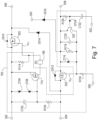
- the rectifier circuit may comprise: (1) first and second input terminals (e.g., AC input terminals); (2) first and second output terminals (e.g., DC output terminals); (3) a first diode configured to conduct current from the first input terminal to the first output terminal; (4) a second diode configured to conduct current from the second output terminal to the second input terminal; (5) a third diode configured to conduct current from the second input terminal to the first output terminal; (6) a fourth diode configured to conduct current from the second output terminal to the first input terminal; (7) a first controllable switching circuit (e.g., a MOSFET) coupled in parallel with the first diode; and (8) a second controllable switching circuit (e.g., a MOSFET) coupled in parallel with the second diode.
- the first and second switching circuits may be rendered non-conductive when a voltage across the input terminals is an AC voltage and rendered conductive when the voltage across the input terminals is a DC voltage.
- the rectifier circuit may also comprise a DC detect circuit that may be electrically coupled between the input terminals and may be configured to render the first and second controllable switching circuits conductive when the voltage across the DC detect circuit is a DC voltage.
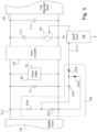
- Fig. 1 is a simplified block diagram of a load control device, e.g., a light-emitting diode (LED) driver 100, for controlling the amount of power delivered to an electrical load, such as an LED light source 102 (e.g., an LED light engine), and thus the intensity of the electrical load.
- an LED light source 102 e.g., an LED light engine
- the LED light source 102 is shown as a plurality of LEDs connected in series, but may comprise a single LED, or a plurality of LEDs connected in parallel, or a suitable combination thereof, depending on the particular lighting system.
- the LED light source 102 may comprise one or more organic light-emitting diodes (OLEDs).
- OLEDs organic light-emitting diodes
- the LED driver 100 may comprise a first input terminal 104 (e.g., a hot terminal) and a second input terminal 106 (e.g., a neutral terminal) that are adapted to be coupled to a power source (not shown), such as, e.g., an alternating-current (AC) power source, or a direct-current (DC) power source.
- a power source such as, e.g., an alternating-current (AC) power source, or a direct-current (DC) power source.
- the first and second input terminals 104, 106 may be configured to receive an input voltage V IN , e.g., an AC mains input voltage, or a DC input voltage.
- the LED driver 100 may comprise a radio-frequency (RFI) filter circuit 110, a rectifier circuit 120, a boost converter 130, a load regulation circuit 140, a control circuit 150, a current sense circuit 160, a memory 170, a communication circuit 172, and/or a power supply 180.
- the RFI filter circuit 110 may minimize the noise provided on the AC mains.
- the rectifier circuit 120 may be a dynamic rectifier circuit configured to change its operation in response to whether an AC voltage or a DC voltage is present at the input terminals 104, 106 (as will be described in greater detail below with reference to Figs. 4 and 5 ).
- the rectifier circuit 120 may be configured to rectify the input voltage V IN to generate a rectified voltage V RECT when the input terminals are connected to an AC power source and an AC voltage is present at the input terminals 104, 106.
- the rectifier circuit 120 may be configured to pass through the input voltage V IN ( e.g., not rectify the input voltage V IN ) when the input terminals are connected to a DC power source and a DC voltage is present at the input terminals 104, 106.
- the boost converter 130 may receive the rectified voltage V RECT and generate a boosted direct-current (DC) bus voltage V BUS across a bus capacitor C BUS (such as, e.g., an electrolytic capacitor).
- the boost converter 130 may comprise any suitable power converter circuit for generating an appropriate bus voltage, such as, for example, a flyback converter, a single-ended primary-inductor converter (SEPIC), a ⁇ uk converter, or other suitable power converter circuit.
- SEPIC single-ended primary-inductor converter
- the boost converter 130 may operate as a power factor correction (PFC) circuit to adjust the power factor of the LED driver 100 towards a power factor of one.
- the LED driver 100 may comprise an input capacitor C IN (such as, e.g., a film capacitor) coupled across the input of the boost converter 130.
- LED drivers having boost converters are described in greater detail in commonly-assigned U.S. Patent No. 8,492,987, issued July 23, 2013 , and U.S Patent No. 8,680,787, issued March 25, 2014 , both entitled LOAD CONTROL DEVICE FOR A LIGHT-EMITTING DIODE LIGHT SOURCE.
- the load regulation circuit 140 may receive the bus voltage V BUS and control the amount of power delivered to the LED light source 102, for example, to control the intensity of the LED light source 102 between a low-end (i.e., minimum) intensity L LE (e.g., approximately 1-5%) and a high-end ( i.e., maximum) intensity L HE ( e.g., approximately 100%).
- An example of the load regulation circuit 140 may be an isolated, half-bridge forward converter.
- An example of the load control device (e.g., LED driver 100) comprising a forward converter is described in greater detail in commonly-assigned U.S. Patent No.
- the load regulation circuit 140 may comprise, for example, a buck converter, a linear regulator, or any suitable LED drive circuit for adjusting the intensity of the LED light source 102.
- the control circuit 150 may be configured to control the operation of the boost converter 130 and/or the load regulation circuit 140.
- the control circuit 150 may comprise, for example, a digital controller or any other suitable processing device, such as, for example, a microcontroller, a programmable logic device (PLD), a microprocessor, an application specific integrated circuit (ASIC), or a field-programmable gate array (FPGA).
- the control circuit 150 may generate a bus voltage control signal V BUS-CNTL , which may be provided to the boost converter 130 for adjusting the magnitude of the bus voltage V BUS towards a target bus voltage V BUS-TARGET .
- the control circuit 150 may receive a bus voltage feedback control signal V BUS-FB from the boost converter 130, which may indicate the magnitude of the bus voltage V BUS .
- the control circuit 150 may adjust an operating frequency f OP and/or a duty cycle DC INV (e.g., an on-time T ON as a percentage of the period T) of the drive control signals V DR1 , V DR2 to adjust the magnitude of the load voltage V LOAD and/or the load current I LOAD .
- the control circuit 150 may receive a load voltage feedback signal V V-LOAD generated by the load regulation circuit 140.
- the load voltage feedback signal V V-LOAD may indicate the magnitude of the load voltage V LOAD .
- the current sense circuit 160 may receive a sense voltage V SENSE generated by the load regulation circuit 140.
- the sense voltage V SENSE may indicate the magnitude of the load current I LOAD .
- the current sense circuit 160 may receive a signal-chopper control signal V CHOP from the control circuit 150.
- the current sense circuit 160 may generate a load current feedback signal V I-LOAD , which may be a DC voltage indicating the average magnitude I AVE of the load current I LOAD .
- the control circuit 150 may receive the load current feedback signal V I-LOAD from the current sense circuit 160 and control the drive control signals V DR1 , V DR2 accordingly.
- control circuit 150 may control the drive control signals V DR1 , V DR2 to adjust a magnitude of the load current I LOAD to a target load current I TRGT to thus control the intensity of the LED light source 102 to the target intensity L TRGT ( e.g. , using a control loop).
- the control circuit 150 may be configured to determine a load power P LOAD presently being consumed by the LED light source 102 using the load voltage feedback signal V V-LOAD and the load current feedback signal V I-LOAD .
- the load current I LOAD may be the current that is conducted through the LED light source 120.
- the target load current I TRGT may be the desired current that the control circuit 150 would ideally cause to be conducted through the LED light source 120 ( e.g., based at least on the load current feedback signal V I-LOAD ).
- the control circuit 150 may be coupled to the memory 170.
- the memory 170 may store operational characteristics of the LED driver 100 (such as, e.g., the target intensity L TRGT , the low-end intensity L LE , the high-end intensity L HE , etc .).
- the communication circuit 172 may be coupled to, for example, a wired communication link, or a wireless communication link, such as a radio-frequency (RF) communication link or an infrared (IR) communication link.
- the control circuit 150 may be configured to update the target intensity L TRGT of the LED light source 102 and/or the operational characteristics stored in the memory 170 in response to digital messages received via the communication circuit 172.
- the LED driver 100 may be operable to receive a phase-control signal from a dimmer switch for determining the target intensity L TRGT for the LED light source 102.
- the power supply 180 may receive the rectified voltage V RECT and generate a direct-current (DC) supply voltage Vcc for powering the circuitry of the LED driver 100.
- the LED driver 100 may also comprise a ripple detect circuit 190, which may receive the rectified voltage V RECT and may generate a ripple detect signal V RIP-DET that may indicate whether AC ripple is present in the rectified voltage V RECT ( i.e., whether an AC voltage is coupled to the input terminals 104, 106).
- the control circuit 150 may receive the ripple detect signal V RIP-DET , and may operate in an AC mode if an AC voltage is coupled to the input terminals 104, 106, or a DC mode if a DC voltage is coupled to the input terminals.
- the ripple detect circuit 190 may also be coupled to receive the input voltage V IN and/or the bus voltage V BUS .
- the LED driver 100 may also comprise a controllable switching circuit 192 (e.g., including a MOSFET) electrically coupled in series with the bus capacitor C BUS for disconnecting the bus capacitor, as will be described in greater detail below.
- the control circuit 150 may enable the operation of the boost converter 130 to generate the bus voltage V BUS across the bus capacitor C BUS .
- the control circuit 150 may render the controllable switching circuit 192 conductive and may control the magnitude of the bus voltage V BUS to a maximum magnitude V BUS-MAX ( e.g. , approximately 465 volts).
- the control circuit 150 may also operate the boost converter 130 as a PFC circuit during the AC mode to adjust the power factor of the LED driver 100 towards a power factor of one.
- the control circuit 150 may be configured to disable the operation of the boost converter 130 to reduce power loss in the LED driver 100, for example, due to the power loss in the boost converter when enabled.
- the boost converter 130 may pass through the DC voltage from the input terminals 104, 106, and the bus voltage V BUS may have a minimum magnitude V BUS-MIN ( e.g. , approximately 380 volts).
- the control circuit 150 may be configured to enable the boost converter 130 during a startup routine of the LED driver 100, and disable the boost converter during normal operation.
- the control circuit 150 may render the controllable switching circuit 192 non-conductive to disconnect the bus capacitor C BUS in the DC mode because the bus capacitor C BUS may not be required when a DC voltage is present at the input terminals 104, 106.
- the LED driver 100 may also comprise a capacitor C FILM (e.g., a film capacitor) coupled across the input of the load regulation circuit 140 for supplying high-frequency current that may be required to circulate through the load regulation circuit. Because the bus capacitor C BUS may comprise one or more electrolytic capacitors, disconnecting the bus capacitor C BUS may increase the lifetime of the LED driver 100. In addition, disconnecting the bus capacitor C BUS may reduce an inrush current conducted by the LED driver 100 when power is first applied to the input terminals 104, 106.
- the control circuit 150 may also enable the operation of the boost converter 130 in the DC mode when the power P LOAD required by LED light source 102 exceeds a threshold amount P TH (e.g. , approximately 80%).
- the control circuit 150 may also be configured to control the target bus voltage V BUS-TARGET as a function of the power P LOAD required by LED light source 102, for example, as shown in Fig. 2 .
- the control circuit 150 may be configured to adjust the target bus voltage V BUS-TARGET linearly between the minimum magnitude V BUS-MIN and the maximum magnitude V BUS-MAX when the power P LOAD required by LED light source 102 is above the threshold amount P TH .
- the control circuit 150 may be configured to control the target bus voltage V BUS-TARGET using open loop control, for example, by using a lookup table to determine the target bus voltage V BUS-TARGET in response to the target intensity L TRGT and/or target load current I TRGT .
- the control circuit 150 may also be configured to control the target bus voltage V BUS-TARGET using closed loop control, for example, by using the load voltage feedback signal V V-LOAD and the load current feedback signal V I-LOAD to determine the power P LOAD required by LED light source 102.
- the control circuit 150 may be configured to learn the target intensity L TRGT and/or the target load current I TRGT at which the power P LOAD required by LED light source 102 exceeds the threshold amount P TH ( e.g., during a startup routine).
- the inverter voltage V INV may be coupled to the primary winding of a transformer 420 through a DC-blocking capacitor C416 (e.g., which may have a capacitance of approximately 0.047 ⁇ F), such that a primary voltage V PRI is generated across the primary winding.
- the transformer 420 may be characterized by a turns ratio n TURNS ( i.e., N 1 /N 2 ), which may be approximately 115:29.
- a sense voltage V SENSE may be generated across a sense resistor R422, which may be coupled in series with the primary winding of the transformer 420.
- the gate of the transistor Q436 may be coupled to circuit common through a resistor R438 ( e.g. , which may have a resistance of approximately 22 k ⁇ ).
- the gate of the transistor Q436 may receive the signal-chopper control signal V CHOP from the control circuit 150.
- An example of the current sense circuit 460 may be described in greater detail in commonly-assigned No. 9,232,574, issued January 5, 2016 , entitled FORWARD CONVERTER HAVING A PRIMARY-SIDE CURRENT SENSE CIRCUIT.
- the second diode 512 may be electrically coupled between the second input terminal 504 and the second output terminal 508, and may be configured to conduct current from the second output terminal 508 to the second input terminal 504.
- the third diode 514 may be electrically coupled between the second input terminal 504 and the first output terminal 506, and may be configured to conduct current from the second input terminal 504 to the first output terminal 506.
- the fourth diode 516 may be electrically coupled between the first input terminal 502 and the second output terminal 508, and may be configured to conduct current from the second output terminal 508 to the first input terminal 502.
- the rectifier circuit 500 may further comprise a rectifier control circuit, such as a DC detect circuit 530, coupled between the input terminals 502, 504 to receive the voltage across the input terminals.
- the DC detect circuit 530 may be configured to generate gate drive voltages V G1 , V G2 that may be coupled to gate terminals of the MOSFETs of the first and second controllable switching circuits 520, 522, respectively, for rendering the first and second controllable switching circuits conductive and non-conductive.
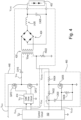
- Fig. 7 is an example diagram of a DC detect circuit 700 for an LED driver.
- the DC detect circuit 700 may be an example of the DC detect circuit 530 of Fig. 5 .
- the DC detect circuit 700 may be part of a rectifier circuit, such as the rectifier circuit 500 shown in Fig. 5 .
- the DC detect circuit 700 may include two input terminals, such as the first and second input terminals 502, 504 ( e.g., AC input terminals) of the rectifier circuit 500.
- the DC detect circuit may be connected to two output terminals through an AC/DC rectifier circuit, such as the first and second output terminals 506, 508 ( e.g., DC output terminals) of the rectifier circuit 500.
- the DC detect circuit 700 may be configured to generate gate drive voltages for controlling controllable switching circuits, such as the gate drive voltages V G1 , V G2 that are coupled to gate terminals of the MOSFETs of the first and second controllable switching circuits 520, 522, respectively, for rendering the first and second controllable switching circuits conductive and non-conductive.
- the DC detect circuit may operate whether it is coupled to an AC voltage or to a DC voltage via the input terminals 502, 504.
- the DC detect circuit 700 may include capacitors C702, C720, and C722, resistors R704, R714, R718, R726, and R730, Zener diodes Z706, Z708, and Z716, a diode D724, a MOSFET 710, and an NPN transistor 728.
- the DC detect circuit 700 may include a power supply, or use a power supply of the LED drive, such as the power supply 180, for example.
- the combination of the capacitor C702 and resistor R704 will cause there to be a net zero DC voltage across the capacitor C702.
- the MOSFET 520 will be non-conductive and in diode mode across diode 510.
- the combination of the capacitor C722 and resistor R726 will cause there to be a net zero DC voltage across the capacitor C722.
- the NPN transistor 728 may see pulsing currents at its gate, rendering the NPN transistor 728 conductive and causing the capacitor C720 to discharge.
- the discharge of the capacitor C720 may cause the MOSFET 522 to be rendered non-conductive and in diode mode across the diode 512. Accordingly, when an AC voltage is coupled to the input terminals 502, 504, the DC detect circuit will not drive either of the MOSFETs 520, 522 to be conductive such that the diodes 510, 512, 514, 516 act as a full-wave rectifier.
- the Zener diodes Z706, Z708 When a DC voltage is coupled to the input terminals 502, 504, the Zener diodes Z706, Z708 will clamp the input DC voltage and cause the capacitor C702 to charge.
- the MOSFET 710 When the capacitor C702 is charged, the MOSFET 710 will turn on, which will drive the first gate drive voltage V G1 towards a supply voltage Vcc ( e.g., as generated by the power supply 180 of the LED driver 100 in Fig. 1 ) and render the MOSFET 520 conductive.
- Vcc e.g., as generated by the power supply 180 of the LED driver 100 in Fig. 1
- the capacitor C722 when a DC voltage is coupled to the input terminals 502, 504, the capacitor C722 will charge and there will not be pulsing currents flowing through R726 ( e.g., as is seen when AC voltage is coupled to the input terminals).
- Fig. 8 is a simplified flowchart of an example control procedure 800 that may be executed by a control circuit of a load control device (e.g., the control circuit 150 of the LED driver 100).
- the control procedure 800 may be executed periodically to control the LED driver to operate in an AC mode or a DC mode in response to ripple detected on an input voltage of the LED driver.
- the control circuit may determine whether the ripple detect signal V RIP-DET indicates that AC voltage or DC voltage is coupled to the input terminals ( e.g. , the input terminals 104, 106). If the control circuit determines that AC voltage is coupled to the input terminals at 802, then the control circuit may operate in AC mode at 804. For example, the control circuit may ensure that the bus capacitor is connected at 806. For instance, the control circuit may connect the bus capacitor by closing a switch ( e.g. , the controllable switching circuit 192) at 806. The control circuit may also enable the boost converter at 808, and set the target bus voltage to V BUS-MAX at 810.
- the control circuit may enable the boost converter at 820.
- the control circuit may set the target bus voltage according to the power required.
- the control circuit may be configured to control the target bus voltage V BUS-TARGET as a function of the power P LOAD required by LED light source 102.
- the control circuit may be configured to adjust the target bus voltage V BUS-TARGET linearly between the minimum magnitude V BUS-MIN and the maximum magnitude V BUS-MAX when the power P LOAD required by LED light source is above the threshold amount P TH .
Landscapes
- Engineering & Computer Science (AREA)
- Power Engineering (AREA)
- Circuit Arrangement For Electric Light Sources In General (AREA)
Claims (12)
- Laststeuervorrichtung (100) zum Steuern von Leistung, die von einer Leistungsquelle an eine elektrische Last (102) geliefert wird, wobei die Laststeuervorrichtung (100) konfiguriert ist, um eine Eingangsspannung von der Leistungsquelle zu empfangen, wobei die Laststeuervorrichtung (100) Folgendes umfasst:einen Leistungswandler (130), der konfiguriert ist, um eine Busspannung zu erzeugen;eine Lastregelungsschaltung (140), die konfiguriert ist, um die Busspannung zu empfangen und die an die elektrische Last (102) gelieferte Leistung zu steuern;eine Gleichrichterschaltung (120, 500), die konfiguriert ist, um die Eingangsspannung von der Leistungsquelle zu empfangen, wobei die Gleichrichterschaltung konfiguriert ist, um die Eingangsspannung gleichzurichten, um eine gleichgerichtete Spannung zu erzeugen, wenn die Eingangsspannung eine Wechselspannung ist, wobei die Gleichrichterschaltung (120, 500) konfiguriert ist, um die Eingangsspannung durchzuleiten, wenn die Eingangsspannung eine Gleichspannung ist,eine Steuerschaltung (150), die konfiguriert ist, um die Lastregelungsschaltung (140) zu steuern, um die an die elektrische Last (102) gelieferte Leistung zu steuern, wobei die Steuerschaltung (150) konfiguriert ist, um in einem AC-Modus zu arbeiten, wenn die Eingangsspannung eine Wechselspannung ist,oder in einem DC-Modus, wenn die Eingangsspannung eine Gleichspannung ist;dadurch gekennzeichnet, dassdie Gleichrichterschaltung (120, 500) erste und zweite steuerbare Schaltschaltungen (520, 522) umfasst, wobei die ersten und zweiten steuerbaren Schaltschaltungen (520, 522) so angeordnet sind, dass sie nichtleitend gemacht werden, wenn die Eingangsspannung eine Wechselspannung ist, und so angeordnet sind, dass sie leitend gemacht werden, wenn die Eingangsspannung eine Gleichspannung ist; undwobei die Steuerschaltung (150), wenn sie im DC-Modus während des normalen Betriebs arbeitet, ferner konfiguriert ist, um den Leistungswandler (130) zu deaktivieren, wenn eine von der elektrischen Last (102) benötigte Leistung kleiner oder gleich einem vorbestimmten Schwellenwert ist.
- Laststeuervorrichtung (100) nach Anspruch 1, wobei die Gleichrichterschaltung (120, 500) ferner Folgendes umfasst erste und zweite Eingangsanschlüsse (502, 504);erste und zweite Ausgangsanschlüsse (506, 508);eine erste Diode (D510), die konfiguriert ist, um Strom von dem ersten Eingangsanschluss (502) zu dem ersten Ausgangsanschluss (506) zu leiten;eine zweite Diode (D512), die konfiguriert ist, um Strom von dem zweiten Ausgangsanschluss (508) zu dem zweiten Eingangsanschluss (504) zu leiten;eine dritte Diode (D514), die konfiguriert ist, um Strom von dem zweiten Eingangsanschluss (504) zu dem ersten Ausgangsanschluss (506) zu leiten;eine vierte Diode (D516), die konfiguriert ist, um Strom von dem zweiten Ausgangsanschluss (508) zu dem ersten Eingangsanschluss (502) zu leiten;wobei die erste steuerbare Schaltschaltung (520) parallel zu der ersten Diode (D510) gekoppelt ist unddie zweite steuerbare Schaltschaltung (522) parallel zu der zweiten Diode (D512) gekoppelt ist; undwobei die ersten und zweiten Schaltschaltungen (520, 522) nichtleitend gemacht werden, wenn die Eingangsspannung eine Wechselspannung ist, und leitend gemacht werden, wenn die Eingangsspannung eine Gleichspannung ist,wobei die Eingangsspannung eine Spannung über den ersten und zweiten Eingangsanschlüssen (502, 504) ist.
- Laststeuervorrichtung (100) nach Anspruch 2, wobei die ersten und zweiten steuerbaren Schaltschaltungen (520, 522) jeweils einen MOSFET umfassen.
- Laststeuervorrichtung (100) nach Anspruch 3, wobei die ersten und zweiten Dioden (D510, D512) Körperdioden der MOSFETs der ersten und zweiten steuerbaren Schaltschaltungen (520, 522) sind.
- Laststeuervorrichtung (100) nach Anspruch 2, wobei die Gleichrichterschaltung (120, 500) eine DC-Erfassungsschaltung (530) umfasst, die elektrisch zwischen den ersten und zweiten Eingangsanschlüssen (502, 504) der Gleichrichterschaltung (120, 500) gekoppelt ist, wobei die DC-Erfassungsschaltung (530) konfiguriert ist, um die ersten und zweiten steuerbaren Schaltschaltungen (520, 522) der Gleichrichterschaltung (120, 500) leitend zu machen, wenn die Spannung über der DC-Erfassungsschaltung (530) eine Gleichspannung ist.
- Laststeuervorrichtung (100) nach Anspruch 1, wobei, wenn sie im DC-Modus während des normalen Betriebs arbeitet, die Steuerschaltung (150) ferner konfiguriert ist, um den Leistungswandler (130) zu steuern, um die Größe der Busspannung auf eine Zielbusspannung einzustellen, wenn die von der elektrischen Last (102) benötigte Leistung größer als der vorbestimmte Schwellenwert ist.
- Laststeuervorrichtung (100) nach Anspruch 1, ferner umfassend:eine Welligkeitserfassungsschaltung (190), die konfiguriert ist, um eine gleichgerichtete Spannung zu empfangen und ein Welligkeitserfassungssignal zu erzeugen, das angibt, ob in der gleichgerichteten Spannung eine AC-Welligkeit vorhanden ist;wobei die Steuerschaltung (150) ferner konfiguriert ist, um das Welligkeitserfassungssignal zu empfangen und basierend auf dem Welligkeitserfassungssignal zu bestimmen, ob die Eingangsspannung eine AC-Spannung oder eine DC-Spannung ist.
- Laststeuervorrichtung (100) nach Anspruch 1, wobei die Steuerschaltung (150) ferner konfiguriert ist, um den Leistungswandler (130) während einer Startroutine der Laststeuervorrichtung zu aktivieren.
- Die Laststeuervorrichtung (100) nach Anspruch 1, ferner umfassend:einen Buskondensator; undeine dritte steuerbare Schaltschaltung (192), die elektrisch in Reihe mit dem Buskondensator gekoppelt ist, wobei die Steuerschaltung (150) ferner konfiguriert ist, um die dritte steuerbare Schaltschaltung (192) nichtleitend zu machen, wenn sie im DC-Modus arbeitet, um den Buskondensator abzutrennen.
- Laststeuervorrichtung (100) nach Anspruch 1, wobei die Steuerschaltung (150) ferner konfiguriert ist, um ein Busspannungssteuersignal zu erzeugen und das Busspannungssteuersignal an den Leistungswandler (130) zu liefern; und
wobei der Leistungswandler (130) ferner konfiguriert ist, um eine Größe der Busspannung basierend auf dem Busspannungssteuersignal auf eine Zielbusspannung einzustellen. - Laststeuervorrichtung (100) nach Anspruch 1, wobei der Leistungswandler (130) ferner konfiguriert ist, um ein Busspannungs-Rückkopplungssteuersignal zu erzeugen, das eine Größe der Busspannung angibt, und das Busspannungs-Rückkopplungssteuersignal an die Steuerschaltung (150) zu liefern.
- Laststeuervorrichtung (100) nach Anspruch 1, wobei die Steuerschaltung (150) ferner konfiguriert ist, um den Leistungswandler (130) zu deaktivieren, indem sie es der DC-Spannung ermöglicht, den Leistungswandler (130) zu durchlaufen, so dass die Busspannung eine minimale Busspannungsgröße aufweist.
Applications Claiming Priority (2)
| Application Number | Priority Date | Filing Date | Title |
|---|---|---|---|
| US201662327198P | 2016-04-25 | 2016-04-25 | |
| PCT/US2017/029477 WO2017189619A1 (en) | 2016-04-25 | 2017-04-25 | Load control device for a light-emitting diode light source |
Publications (2)
| Publication Number | Publication Date |
|---|---|
| EP3449695A1 EP3449695A1 (de) | 2019-03-06 |
| EP3449695B1 true EP3449695B1 (de) | 2025-07-02 |
Family
ID=58699272
Family Applications (1)
| Application Number | Title | Priority Date | Filing Date |
|---|---|---|---|
| EP17722939.0A Active EP3449695B1 (de) | 2016-04-25 | 2017-04-25 | Laststeuerungsvorrichtung für eine leuchtdiodenlichtquelle |
Country Status (6)
| Country | Link |
|---|---|
| US (4) | US10397991B2 (de) |
| EP (1) | EP3449695B1 (de) |
| CN (1) | CN109196952B (de) |
| CA (1) | CA3022128C (de) |
| MX (2) | MX2022008886A (de) |
| WO (1) | WO2017189619A1 (de) |
Families Citing this family (15)
| Publication number | Priority date | Publication date | Assignee | Title |
|---|---|---|---|---|
| CA3221357A1 (en) | 2016-07-22 | 2018-01-25 | Lutron Technology Company Llc | Modular lighting panel |
| CN106409220B (zh) * | 2016-09-29 | 2019-01-29 | 深圳创维-Rgb电子有限公司 | 一种oled驱动电源装置及oled电视 |
| CN112602379B (zh) * | 2018-06-26 | 2023-10-20 | 路创技术有限责任公司 | 具有可控滤波器电路的负载控制装置 |
| CN109547721B (zh) * | 2018-12-25 | 2021-06-01 | 深圳创维-Rgb电子有限公司 | 一种电视电源驱动装置和电视机 |
| CN110022052B (zh) * | 2019-05-24 | 2020-07-10 | 珠海格力电器股份有限公司 | 驱动系统、空调设备、控制方法和控制器 |
| JP7689944B2 (ja) * | 2019-07-19 | 2025-06-09 | シグニファイ ホールディング ビー ヴィ | スタンバイモードにおいて電力損失を最小限に抑えながらdcバス電圧を検出するためのシステム及び方法 |
| EP3772870B1 (de) * | 2019-08-06 | 2025-02-12 | Xiamen Eco Lighting Co., Ltd. | Lichtsensoransteuerungsschaltung und lampe |
| US11743988B2 (en) * | 2020-11-11 | 2023-08-29 | Shanghai Lumixess Lighting Technology Company | Power adjusting circuit, LED power supply and LED luminaire |
| US12470138B2 (en) | 2021-05-25 | 2025-11-11 | Nissan Motor Co., Ltd. | Load control device, load control system, and load control method |
| CA3223033A1 (en) * | 2021-07-15 | 2023-01-19 | Ari L. FOX | Power supply device with over-power protection |
| CN116232056A (zh) * | 2021-12-06 | 2023-06-06 | 台达电子企业管理(上海)有限公司 | 功率变换装置与电压控制方法 |
| US20250125612A1 (en) * | 2022-03-18 | 2025-04-17 | Nippon Telegraph And Telephone Corporation | Control apparatus, control method, and program |
| WO2023193027A2 (en) * | 2022-04-01 | 2023-10-05 | DMF, Inc. | Low-voltage lighting systems |
| EP4387399B1 (de) * | 2022-12-13 | 2025-07-02 | Tridonic GmbH & Co KG | Überspannungsschutzschaltung und stromversorgung zum betrieb aus einem gleichstromnetz |
| CN117769074B (zh) * | 2023-12-27 | 2024-11-01 | 瑞飞光电子(深圳)有限公司 | 一种二极管的智能控制电路 |
Citations (3)
| Publication number | Priority date | Publication date | Assignee | Title |
|---|---|---|---|---|
| US6181588B1 (en) * | 1998-09-25 | 2001-01-30 | Dell Usa, L.P. | Constant polarity input device including synchronous bridge rectifier |
| US20110241569A1 (en) * | 2008-11-14 | 2011-10-06 | Tridonic Gmbh & Co. Kg | Adaptive Pfc For A Lighting Means Load Circuit, In Particular For A Load Circuit With An Led |
| US20120001599A1 (en) * | 2010-06-30 | 2012-01-05 | Masayasu Tanaka | Power Supply Circuit Capable of Handling Direct Current and Alternating Current and Power Supply Control Method |
Family Cites Families (26)
| Publication number | Priority date | Publication date | Assignee | Title |
|---|---|---|---|---|
| US4331994A (en) * | 1979-09-28 | 1982-05-25 | Borg-Warner Corporation | Shootthrough fault protection system for a voltage source transistor inverter |
| US5196995A (en) * | 1989-12-01 | 1993-03-23 | Zdzislaw Gulczynski | 3-terminal bidirectional switching power supply with AC or DC input and AC or DC output |
| US6366474B1 (en) * | 2000-09-29 | 2002-04-02 | Jeff Gucyski | Switching power supplies incorporating power factor correction and/or switching at resonant transition |
| US7075254B2 (en) | 2004-12-14 | 2006-07-11 | Lutron Electronics Co., Inc. | Lighting ballast having boost converter with on/off control and method of ballast operation |
| US7609040B1 (en) * | 2005-10-31 | 2009-10-27 | Chil Semiconductor Corporation | Power supply and related circuits |
| FR2895383B1 (fr) * | 2005-12-27 | 2010-03-12 | Sidel Sa | Convoyeur ou transporteur a air |
| US9231402B2 (en) * | 2007-12-26 | 2016-01-05 | Silicon Laboratories Inc. | Circuit device and method of suppressing a power event |
| US8228001B2 (en) * | 2009-02-24 | 2012-07-24 | Suntec Enterprises | Method and apparatus of driving LED and OLED devices |
| US8866401B2 (en) | 2009-03-06 | 2014-10-21 | Lutron Electronics Co., Inc. | Multi-stage power supply for a load control device having a low-power mode |
| US8466628B2 (en) | 2009-10-07 | 2013-06-18 | Lutron Electronics Co., Inc. | Closed-loop load control circuit having a wide output range |
| EP2522068A2 (de) * | 2010-01-08 | 2012-11-14 | Holdip Limited | Verbesserungen im zusammenhang mit gleichrichterschaltungen |
| US8369111B2 (en) * | 2010-08-02 | 2013-02-05 | Power Integrations, Inc. | Ultra low standby consumption in a high power power converter |
| US8593076B2 (en) | 2010-08-18 | 2013-11-26 | Lutron Electronics Co., Inc. | Electronic dimming ballast having advanced boost converter control |
| US8680787B2 (en) * | 2011-03-15 | 2014-03-25 | Lutron Electronics Co., Inc. | Load control device for a light-emitting diode light source |
| DE102012203745A1 (de) | 2011-12-23 | 2013-06-27 | Tridonic Gmbh & Co. Kg | Verfahren und Schaltungsanordnung zum Betrieb von Leuchtmitteln |
| US8975825B2 (en) * | 2012-05-08 | 2015-03-10 | Cree, Inc. | Light emitting diode driver with isolated control circuits |
| US9232574B2 (en) | 2012-07-06 | 2016-01-05 | Lutron Electronics Co., Inc. | Forward converter having a primary-side current sense circuit |
| US9462660B2 (en) | 2013-02-26 | 2016-10-04 | Lutron Electronics Co., Inc. | Controlling an electronic dimming ballast during low temperature or low mercury conditions |
| US9113521B2 (en) | 2013-05-29 | 2015-08-18 | Lutron Electronics Co., Inc. | Load control device for a light-emitting diode light source |
| US9345088B2 (en) * | 2013-06-07 | 2016-05-17 | Texas Instruments Incorporated | LED control circuits and methods |
| US9247608B2 (en) | 2013-11-08 | 2016-01-26 | Lutron Electronics Co., Inc. | Load control device for a light-emitting diode light source |
| CN103944394A (zh) * | 2014-03-26 | 2014-07-23 | 东莞市冠日光电科技有限公司 | Led开关电源控制器集成电路 |
| US9793796B2 (en) * | 2015-02-23 | 2017-10-17 | Infineon Technologies Austria Ag | Driver controller with AC-adapted and DC-adapted control modes |
| US9565731B2 (en) | 2015-05-01 | 2017-02-07 | Lutron Electronics Co., Inc. | Load control device for a light-emitting diode light source |
| EP3311633B1 (de) | 2015-06-19 | 2024-09-04 | Lutron Technology Company LLC | Laststeuerungsvorrichtung für eine leuchtdiodenlichtquelle |
| JP6604863B2 (ja) * | 2016-02-05 | 2019-11-13 | ローム株式会社 | 受電装置およびそのコントローラ、それを用いた電子機器、給電システムの制御方法 |
-
2017
- 2017-04-25 EP EP17722939.0A patent/EP3449695B1/de active Active
- 2017-04-25 CN CN201780032529.3A patent/CN109196952B/zh active Active
- 2017-04-25 WO PCT/US2017/029477 patent/WO2017189619A1/en not_active Ceased
- 2017-04-25 US US15/496,932 patent/US10397991B2/en active Active
- 2017-04-25 CA CA3022128A patent/CA3022128C/en active Active
-
2018
- 2018-10-24 MX MX2022008886A patent/MX2022008886A/es unknown
- 2018-10-24 MX MX2022012160A patent/MX2022012160A/es unknown
-
2019
- 2019-08-05 US US16/532,365 patent/US10827586B2/en active Active
-
2020
- 2020-10-28 US US17/083,262 patent/US12082322B2/en active Active
-
2024
- 2024-07-23 US US18/781,054 patent/US20240381506A1/en active Pending
Patent Citations (3)
| Publication number | Priority date | Publication date | Assignee | Title |
|---|---|---|---|---|
| US6181588B1 (en) * | 1998-09-25 | 2001-01-30 | Dell Usa, L.P. | Constant polarity input device including synchronous bridge rectifier |
| US20110241569A1 (en) * | 2008-11-14 | 2011-10-06 | Tridonic Gmbh & Co. Kg | Adaptive Pfc For A Lighting Means Load Circuit, In Particular For A Load Circuit With An Led |
| US20120001599A1 (en) * | 2010-06-30 | 2012-01-05 | Masayasu Tanaka | Power Supply Circuit Capable of Handling Direct Current and Alternating Current and Power Supply Control Method |
Also Published As
| Publication number | Publication date |
|---|---|
| US20210045211A1 (en) | 2021-02-11 |
| CA3022128A1 (en) | 2017-11-02 |
| WO2017189619A1 (en) | 2017-11-02 |
| US12082322B2 (en) | 2024-09-03 |
| MX2022008886A (es) | 2022-08-15 |
| CN109196952B (zh) | 2021-06-18 |
| CN109196952A (zh) | 2019-01-11 |
| US20170311400A1 (en) | 2017-10-26 |
| MX2022012160A (es) | 2022-10-31 |
| US20190364629A1 (en) | 2019-11-28 |
| US10827586B2 (en) | 2020-11-03 |
| US20240381506A1 (en) | 2024-11-14 |
| US10397991B2 (en) | 2019-08-27 |
| EP3449695A1 (de) | 2019-03-06 |
| CA3022128C (en) | 2021-04-06 |
Similar Documents
| Publication | Publication Date | Title |
|---|---|---|
| US12082322B2 (en) | Load control device for a light-emitting diode light source | |
| US8901851B2 (en) | TRIAC dimmer compatible LED driver and method thereof | |
| US8975825B2 (en) | Light emitting diode driver with isolated control circuits | |
| US20100181925A1 (en) | Ballast/Line Detection Circuit for Fluorescent Replacement Lamps | |
| US20110266969A1 (en) | Dimmable LED Power Supply with Power Factor Control | |
| AU2010203058B2 (en) | Switch mode power converter | |
| US20130099686A1 (en) | Light emitting diode (led) dimming system | |
| US20100295478A1 (en) | Led driving circuit | |
| CN104868703A (zh) | 无辅助绕组的高压转换器 | |
| Jha et al. | A PFC modified-landsman converter based PWM-dimmable RGB HB-LED driver for large area projection applications | |
| CN106163037B (zh) | 发光二极管驱动电路和发光二极管照明设备 | |
| US8575847B2 (en) | Control circuit of light-emitting element | |
| Zhang et al. | A high-efficiency quasi-two-stage LED driver with multichannel outputs | |
| JP6320455B2 (ja) | Led点灯装置 | |
| US10624163B1 (en) | Lighting device with output buffer circuit for stability during no-load or standby operation | |
| JP5944672B2 (ja) | Led点灯装置、それを備えた照明器具、及び照明装置 | |
| KR20090056025A (ko) | 엘이디등 전원장치 | |
| JP2020107437A (ja) | 電源装置及び照明システム | |
| JP6791486B2 (ja) | 発光素子駆動装置及びその駆動方法 | |
| HK40002528A (en) | Load control device for a light-emitting diode light source | |
| HK40002528B (zh) | 用於发光二极管光源的负载控制装置 | |
| JP7241312B2 (ja) | 点灯システム、照明制御システム、及び照明器具 | |
| JP7133787B2 (ja) | 点灯システム、照明制御システム、及び照明器具 | |
| US20230029021A1 (en) | Lighting apparatus driver | |
| KR20150006245A (ko) | 디밍 제어가 가능한 led 조명장치 |
Legal Events
| Date | Code | Title | Description |
|---|---|---|---|
| STAA | Information on the status of an ep patent application or granted ep patent |
Free format text: STATUS: UNKNOWN |
|
| STAA | Information on the status of an ep patent application or granted ep patent |
Free format text: STATUS: THE INTERNATIONAL PUBLICATION HAS BEEN MADE |
|
| PUAI | Public reference made under article 153(3) epc to a published international application that has entered the european phase |
Free format text: ORIGINAL CODE: 0009012 |
|
| STAA | Information on the status of an ep patent application or granted ep patent |
Free format text: STATUS: REQUEST FOR EXAMINATION WAS MADE |
|
| 17P | Request for examination filed |
Effective date: 20181122 |
|
| AK | Designated contracting states |
Kind code of ref document: A1 Designated state(s): AL AT BE BG CH CY CZ DE DK EE ES FI FR GB GR HR HU IE IS IT LI LT LU LV MC MK MT NL NO PL PT RO RS SE SI SK SM TR |
|
| AX | Request for extension of the european patent |
Extension state: BA ME |
|
| DAV | Request for validation of the european patent (deleted) | ||
| DAX | Request for extension of the european patent (deleted) | ||
| RAP1 | Party data changed (applicant data changed or rights of an application transferred) |
Owner name: LUTRON TECHNOLOGY COMPANY LLC |
|
| STAA | Information on the status of an ep patent application or granted ep patent |
Free format text: STATUS: EXAMINATION IS IN PROGRESS |
|
| 17Q | First examination report despatched |
Effective date: 20201125 |
|
| REG | Reference to a national code |
Ref country code: DE Ref legal event code: R079 Free format text: PREVIOUS MAIN CLASS: H05B0033080000 Ipc: H05B0045380000 Ref document number: 602017090262 Country of ref document: DE |
|
| GRAP | Despatch of communication of intention to grant a patent |
Free format text: ORIGINAL CODE: EPIDOSNIGR1 |
|
| STAA | Information on the status of an ep patent application or granted ep patent |
Free format text: STATUS: GRANT OF PATENT IS INTENDED |
|
| RIC1 | Information provided on ipc code assigned before grant |
Ipc: H05B 47/165 20200101ALN20250205BHEP Ipc: H05B 45/39 20200101ALN20250205BHEP Ipc: H05B 45/10 20200101ALN20250205BHEP Ipc: H05B 45/382 20200101ALI20250205BHEP Ipc: H05B 45/38 20200101AFI20250205BHEP |
|
| INTG | Intention to grant announced |
Effective date: 20250218 |
|
| RIC1 | Information provided on ipc code assigned before grant |
Ipc: H05B 47/165 20200101ALN20250210BHEP Ipc: H05B 45/39 20200101ALN20250210BHEP Ipc: H05B 45/10 20200101ALN20250210BHEP Ipc: H05B 45/382 20200101ALI20250210BHEP Ipc: H05B 45/38 20200101AFI20250210BHEP |
|
| GRAS | Grant fee paid |
Free format text: ORIGINAL CODE: EPIDOSNIGR3 |
|
| GRAA | (expected) grant |
Free format text: ORIGINAL CODE: 0009210 |
|
| STAA | Information on the status of an ep patent application or granted ep patent |
Free format text: STATUS: THE PATENT HAS BEEN GRANTED |
|
| AK | Designated contracting states |
Kind code of ref document: B1 Designated state(s): AL AT BE BG CH CY CZ DE DK EE ES FI FR GB GR HR HU IE IS IT LI LT LU LV MC MK MT NL NO PL PT RO RS SE SI SK SM TR |
|
| REG | Reference to a national code |
Ref country code: GB Ref legal event code: FG4D |
|
| REG | Reference to a national code |
Ref country code: CH Ref legal event code: EP |
|
| REG | Reference to a national code |
Ref country code: DE Ref legal event code: R096 Ref document number: 602017090262 Country of ref document: DE |
|
| REG | Reference to a national code |
Ref country code: IE Ref legal event code: FG4D |
|
| REG | Reference to a national code |
Ref country code: NL Ref legal event code: MP Effective date: 20250702 |
|
| PG25 | Lapsed in a contracting state [announced via postgrant information from national office to epo] |
Ref country code: PT Free format text: LAPSE BECAUSE OF FAILURE TO SUBMIT A TRANSLATION OF THE DESCRIPTION OR TO PAY THE FEE WITHIN THE PRESCRIBED TIME-LIMIT Effective date: 20251103 |
|
| PG25 | Lapsed in a contracting state [announced via postgrant information from national office to epo] |
Ref country code: NL Free format text: LAPSE BECAUSE OF FAILURE TO SUBMIT A TRANSLATION OF THE DESCRIPTION OR TO PAY THE FEE WITHIN THE PRESCRIBED TIME-LIMIT Effective date: 20250702 |
|
| REG | Reference to a national code |
Ref country code: AT Ref legal event code: MK05 Ref document number: 1810815 Country of ref document: AT Kind code of ref document: T Effective date: 20250702 |
|
| PG25 | Lapsed in a contracting state [announced via postgrant information from national office to epo] |
Ref country code: IS Free format text: LAPSE BECAUSE OF FAILURE TO SUBMIT A TRANSLATION OF THE DESCRIPTION OR TO PAY THE FEE WITHIN THE PRESCRIBED TIME-LIMIT Effective date: 20251102 |
|
| PG25 | Lapsed in a contracting state [announced via postgrant information from national office to epo] |
Ref country code: NO Free format text: LAPSE BECAUSE OF FAILURE TO SUBMIT A TRANSLATION OF THE DESCRIPTION OR TO PAY THE FEE WITHIN THE PRESCRIBED TIME-LIMIT Effective date: 20251002 |
|
| REG | Reference to a national code |
Ref country code: LT Ref legal event code: MG9D |
|
| PG25 | Lapsed in a contracting state [announced via postgrant information from national office to epo] |
Ref country code: AT Free format text: LAPSE BECAUSE OF FAILURE TO SUBMIT A TRANSLATION OF THE DESCRIPTION OR TO PAY THE FEE WITHIN THE PRESCRIBED TIME-LIMIT Effective date: 20250702 |
|
| PG25 | Lapsed in a contracting state [announced via postgrant information from national office to epo] |
Ref country code: FI Free format text: LAPSE BECAUSE OF FAILURE TO SUBMIT A TRANSLATION OF THE DESCRIPTION OR TO PAY THE FEE WITHIN THE PRESCRIBED TIME-LIMIT Effective date: 20250702 |
|
| PG25 | Lapsed in a contracting state [announced via postgrant information from national office to epo] |
Ref country code: HR Free format text: LAPSE BECAUSE OF FAILURE TO SUBMIT A TRANSLATION OF THE DESCRIPTION OR TO PAY THE FEE WITHIN THE PRESCRIBED TIME-LIMIT Effective date: 20250702 |
|
| PG25 | Lapsed in a contracting state [announced via postgrant information from national office to epo] |
Ref country code: GR Free format text: LAPSE BECAUSE OF FAILURE TO SUBMIT A TRANSLATION OF THE DESCRIPTION OR TO PAY THE FEE WITHIN THE PRESCRIBED TIME-LIMIT Effective date: 20251003 |
|
| PG25 | Lapsed in a contracting state [announced via postgrant information from national office to epo] |
Ref country code: SE Free format text: LAPSE BECAUSE OF FAILURE TO SUBMIT A TRANSLATION OF THE DESCRIPTION OR TO PAY THE FEE WITHIN THE PRESCRIBED TIME-LIMIT Effective date: 20250702 Ref country code: CZ Free format text: LAPSE BECAUSE OF FAILURE TO SUBMIT A TRANSLATION OF THE DESCRIPTION OR TO PAY THE FEE WITHIN THE PRESCRIBED TIME-LIMIT Effective date: 20250702 |
|
| PG25 | Lapsed in a contracting state [announced via postgrant information from national office to epo] |
Ref country code: LV Free format text: LAPSE BECAUSE OF FAILURE TO SUBMIT A TRANSLATION OF THE DESCRIPTION OR TO PAY THE FEE WITHIN THE PRESCRIBED TIME-LIMIT Effective date: 20250702 |
|
| PG25 | Lapsed in a contracting state [announced via postgrant information from national office to epo] |
Ref country code: PL Free format text: LAPSE BECAUSE OF FAILURE TO SUBMIT A TRANSLATION OF THE DESCRIPTION OR TO PAY THE FEE WITHIN THE PRESCRIBED TIME-LIMIT Effective date: 20250702 Ref country code: BG Free format text: LAPSE BECAUSE OF FAILURE TO SUBMIT A TRANSLATION OF THE DESCRIPTION OR TO PAY THE FEE WITHIN THE PRESCRIBED TIME-LIMIT Effective date: 20250702 |
|
| PG25 | Lapsed in a contracting state [announced via postgrant information from national office to epo] |
Ref country code: RS Free format text: LAPSE BECAUSE OF FAILURE TO SUBMIT A TRANSLATION OF THE DESCRIPTION OR TO PAY THE FEE WITHIN THE PRESCRIBED TIME-LIMIT Effective date: 20251002 |
|
| PG25 | Lapsed in a contracting state [announced via postgrant information from national office to epo] |
Ref country code: ES Free format text: LAPSE BECAUSE OF FAILURE TO SUBMIT A TRANSLATION OF THE DESCRIPTION OR TO PAY THE FEE WITHIN THE PRESCRIBED TIME-LIMIT Effective date: 20250702 |
|
| PG25 | Lapsed in a contracting state [announced via postgrant information from national office to epo] |
Ref country code: SM Free format text: LAPSE BECAUSE OF FAILURE TO SUBMIT A TRANSLATION OF THE DESCRIPTION OR TO PAY THE FEE WITHIN THE PRESCRIBED TIME-LIMIT Effective date: 20250702 |
|
| PGFP | Annual fee paid to national office [announced via postgrant information from national office to epo] |
Ref country code: GB Payment date: 20260320 Year of fee payment: 10 |
|
| PG25 | Lapsed in a contracting state [announced via postgrant information from national office to epo] |
Ref country code: DK Free format text: LAPSE BECAUSE OF FAILURE TO SUBMIT A TRANSLATION OF THE DESCRIPTION OR TO PAY THE FEE WITHIN THE PRESCRIBED TIME-LIMIT Effective date: 20250702 |
|
| PG25 | Lapsed in a contracting state [announced via postgrant information from national office to epo] |
Ref country code: IT Free format text: LAPSE BECAUSE OF FAILURE TO SUBMIT A TRANSLATION OF THE DESCRIPTION OR TO PAY THE FEE WITHIN THE PRESCRIBED TIME-LIMIT Effective date: 20250702 |
|
| PGFP | Annual fee paid to national office [announced via postgrant information from national office to epo] |
Ref country code: FR Payment date: 20260317 Year of fee payment: 10 |