EP3772870B1 - Lichtsensoransteuerungsschaltung und lampe - Google Patents
Lichtsensoransteuerungsschaltung und lampe Download PDFInfo
- Publication number
- EP3772870B1 EP3772870B1 EP19195911.3A EP19195911A EP3772870B1 EP 3772870 B1 EP3772870 B1 EP 3772870B1 EP 19195911 A EP19195911 A EP 19195911A EP 3772870 B1 EP3772870 B1 EP 3772870B1
- Authority
- EP
- European Patent Office
- Prior art keywords
- module
- main control
- light sensing
- connect
- signal
- Prior art date
- Legal status (The legal status is an assumption and is not a legal conclusion. Google has not performed a legal analysis and makes no representation as to the accuracy of the status listed.)
- Active
Links
Images


Classifications
-
- H—ELECTRICITY
- H05—ELECTRIC TECHNIQUES NOT OTHERWISE PROVIDED FOR
- H05B—ELECTRIC HEATING; ELECTRIC LIGHT SOURCES NOT OTHERWISE PROVIDED FOR; CIRCUIT ARRANGEMENTS FOR ELECTRIC LIGHT SOURCES, IN GENERAL
- H05B45/00—Circuit arrangements for operating light-emitting diodes [LED]
- H05B45/10—Controlling the intensity of the light
- H05B45/14—Controlling the intensity of the light using electrical feedback from LEDs or from LED modules
-
- H—ELECTRICITY
- H03—ELECTRONIC CIRCUITRY
- H03K—PULSE TECHNIQUE
- H03K7/00—Modulating pulses with a continuously-variable modulating signal
- H03K7/08—Duration or width modulation ; Duty cycle modulation
-
- H—ELECTRICITY
- H05—ELECTRIC TECHNIQUES NOT OTHERWISE PROVIDED FOR
- H05B—ELECTRIC HEATING; ELECTRIC LIGHT SOURCES NOT OTHERWISE PROVIDED FOR; CIRCUIT ARRANGEMENTS FOR ELECTRIC LIGHT SOURCES, IN GENERAL
- H05B47/00—Circuit arrangements for operating light sources in general, i.e. where the type of light source is not relevant
- H05B47/10—Controlling the light source
- H05B47/105—Controlling the light source in response to determined parameters
- H05B47/11—Controlling the light source in response to determined parameters by determining the brightness or colour temperature of ambient light
-
- Y—GENERAL TAGGING OF NEW TECHNOLOGICAL DEVELOPMENTS; GENERAL TAGGING OF CROSS-SECTIONAL TECHNOLOGIES SPANNING OVER SEVERAL SECTIONS OF THE IPC; TECHNICAL SUBJECTS COVERED BY FORMER USPC CROSS-REFERENCE ART COLLECTIONS [XRACs] AND DIGESTS
- Y02—TECHNOLOGIES OR APPLICATIONS FOR MITIGATION OR ADAPTATION AGAINST CLIMATE CHANGE
- Y02B—CLIMATE CHANGE MITIGATION TECHNOLOGIES RELATED TO BUILDINGS, e.g. HOUSING, HOUSE APPLIANCES OR RELATED END-USER APPLICATIONS
- Y02B20/00—Energy efficient lighting technologies, e.g. halogen lamps or gas discharge lamps
- Y02B20/40—Control techniques providing energy savings, e.g. smart controller or presence detection
Definitions
- the present application pertains to the technical field of illumination, and particularly relates to a light sensing drive circuit and a lamp.
- a mainstream solution in the market for light sensing lamps using visible light is to connect a MOS transistor in series at an output light source.
- the MOS transistor When the ambient light is relatively bright, the MOS transistor is turned off, and the output voltage at this time is an OVP (Over Votage Protect) voltage which is higher than a normal working voltage.
- OVP Over Votage Protect
- the MOS transistor When the ambient becomes dark, the MOS transistor is turned on, and then there will be a large inrush current in the entire output circuit, thus the circuit reliability is poor.
- the light sensing lamps using visible light are easily affected by a self-illuminating light source, and the light intensity detection is inaccurate.
- US2010327764A1 discloses an illumination device and a method for controlling the illumination device, wherein the illumination device can be controlled to be turned on once ambient light decreased to a certain level or turned off once the ambient light increased to another certain level.
- US2010327764A1 fails to eliminate the influence of light emitted by LEDs of the illumination device on detection for the ambient light.
- An object of the present application is to provide a light sensing drive circuit and a lamp, which aims to solve the problems in the conventional light sensing lamps using visible light that they are easily affected by self-luminescence and that the circuit reliability is poor.
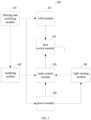
- a light sensing drive circuit which is connected with an LED module, the light sensing drive circuit includes: a filtering and rectifying module, a power module, a light sensing module, a main control module, and a drive module.
- the filtering and rectifying module is configured to connect to a commercial power, and to generate a rectified voltage according to the commercial power.
- the power module is configured to connect with the filtering and rectifying module, and to generate a supply voltage according to the rectified voltage.
- the light sensing module is configured to connect with the power module, and to detect ambient light intensity to generate a light sensing signal.
- the sampling module is configured to connect with the filtering and rectifying module, and to generate a sampling signal according to the rectified voltage.
- the main control module is configured to connect with the light sensing module and the sampling module, and to generate a control signal of a preset duty cycle according to the light sensing signal and the sampling signal when the drive module is turned off by the control signal.
- the drive module includes: a second drive module, an LED module and a switch module.
- the second drive module is configured to connect with the main control module and the filtering and rectifying module, and to generate a driving voltage according to the control signal and the rectified voltage.
- the LED module is configured to connect with the second drive module, and to emit light according to the driving voltage.
- the switch module is configured to connect with the LED module and the control module, and to turn on or turn off the driving voltage based on the preset duty cycle according to the control signal.
- the switch module includes an optoelectronic isolator and a MOS transistor.
- An anode of an illuminator of the optoelectronic isolator is an input end of the switch module for inputting a control signal, a cathode of the illuminator of the optoelectronic isolator is grounded, a first end of a light receptor of the optoelectronic isolator is connected to a DC power supply, a second end of the light receptor of the optoelectronic isolator is connected to a gate of the MOS transistor, a drain of the MOS transistor is connected to a cathode of the LED module, and a source of the MOS transistor is grounded.
- the second drive module includes a driving chip, an inductor, a diode, and a capacitor.
- a drain terminal of the driving chip is connected to a first end of the inductor, a second end of the inductor is connected to the filtering and rectifying module through the capacitor, a control end of the driving chip is an input end of the second drive module for inputting a control signal, an anode of the diode is connected to the first end of the inductor, a cathode of the diode is an input end of the second drive module for inputting a rectified voltage, the second end of the inductor is connected to the switch module, and the inductor is connected to an anode of the LED module through the capacitor.
- the main control module includes a main control chip.
- a first input and output end of the main control chip is an input end of the main control module for inputting a sampling signal
- a second input and output end of the main control chip is an input end of the main control module for inputting a light sensing signal
- a third input and output end of the main control chip is an output end of the main control module for outputting a control signal.
- a lamp is provided, and the lamp includes the above-described light sensing drive circuit.
- the input commercial power is converted into the rectified voltage by the filtering and rectifying module, the rectified voltage is sampled through the sampling module, the ambient light intensity is sensed by the light sensing module, the light sensing signal is generated according to the ambient light intensity and the supply voltage, and the control signal is generated by the main control module according to the light sensing signal and the sampling signal, thereby the drive module is controlled to drive the LED module is.
- the drive module adjusts the driving voltage according to the preset duty cycle of the main control module, and there will not be a large inrush current in the entire output circuit at this time, thereby improving the circuit reliability.
- the sampling module ensures that the chopping points at each time are at the same voltage point of the rectified voltage, so that the current waveform of each cycle will remain the same and no stroboflash visible to human eyes will occur.
- the control signal of the preset duty cycle is generated according to the light sensing signal and the sampling signal when the drive module is turned off by the control signal, that is, the light sensing signal is sampled and acquired when the LED module is turned off, thereby eliminating the effect of self-illumination on the ambient light detection.
- the light sensing drive circuit includes a filtering and rectifying module 10, a power module 20, a light sensing module 30, a sampling module 40, a main control module 50, and a drive module 60.
- the filtering and rectifying module 10 is configured to connect to a commercial power, and to generate a rectified voltage according to the commercial power
- the power module 20 is configured to connect with the filtering and rectifying module 10, and to generate a supply voltage according to the rectified voltage
- the light sensing module 30 is configured to connect with the power module 20, and to detect ambient light intensity according to the supply voltage to generate a light sensing signal
- the sampling module 40 is configured to connect with the filtering and rectifying module 10, and to generate a sampling signal according to the rectified voltage
- the main control module 50 is configured to connect with the light sensing module 30 and the sampling module 40, and to generate a control signal of a preset duty cycle according to the light sensing signal and the sampling signal when the drive module 60 is turned off by a control signal; and
- the input commercial power is converted into the rectified voltage by the filtering and rectifying module 10, the rectified voltage is sampled through the sampling module 40, the ambient light intensity is sensed by the light sensing module 30, the light sensing signal is generated according to the ambient light intensity and the supply voltage, and the control signal of the preset duty cycle is generated according to the light sensing signal and the sampling signal when the drive module 60 is turned off by the control signal, that is, the light sensing signal is sampled and acquired when the LED module 61 is turned off, thereby eliminating the effect of self-illumination on the ambient light detection.
- the drive module 60 adjusts the driving voltage according to the preset duty cycle of the main control module, and there will not be a large inrush current in the entire output circuit at this time, thereby improving the circuit reliability.
- the control signal and the sampling signal have a same phase.
- the sampling module 40 ensures that the chopping points at each time are at the same voltage point of the rectified voltage, and that the control signal and the sampling signal have the same phase, so that the current waveform of each cycle will remain the same and no stroboflash visible to human eyes will occur.
- the drive module 60 includes a first drive module 62 and an LED module 61.
- the first drive module 62 is configured to connect with the main control module 50 and the filtering and rectifying module 10, and to generate the driving voltage according to the control signal and the rectified voltage.
- the LED module 61 is configured to connect with the first drive module 62, and to emit light according to the driving voltage.
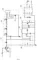
- the first drive module 62 includes a first driving chip U1, a first inductor L1, a first diode D1, and a first capacitor C1.
- a drain terminal of the first driving chip U1 is connected to a first end of the first inductor L1, a second end of the first inductor L1 is connected to the filtering and rectifying module 10 through the first capacitor C1, a control end of the first driving chip U1 is an input end of the first drive module 62 for inputting a control signal, an anode of the first diode D1 is connected to the first end of the first inductor L1, a cathode of the first diode D1 is an input end of the first drive module 62 for inputting a rectified voltage, the second end of the first inductor L1 is connected to the cathode of the LED module 61, and the first inductor L1 is connected to the anode of the LED module 61 through the first capacitor C1.
- the sampling module 40 is configured to detect the rectified voltage, and to generate the sampling signal TS1 through sampling via a first divider resistor R2 and a second divider resistor R3.
- an output end of the main control chip U2 for inputting a sampling signal detects that the voltage of the sampling signal TS1 drops to a first preset value (1.5V)
- an output end of the main control chip U2 for outputting a control signal first outputs a control signal with low level lasting a first preset time of 2ms and the LED module 61 at this time is turned off, and then the output end of the main control chip U2 for outputting a control signal outputs a control signal with high level and the LED module 61 is lit.
- the output end of the main control chip U2 for outputting a control signal outputs the low level lasting the first preset time of 2ms again, and the detection is repeated and circulated.
- the light sensing module 30 is a brightness detection circuit for the ambient light.
- the photosensitive diode CDS1 has a relatively small resistance value, and the voltage of the second end of the photosensitive diode CDS1 is relatively high.
- the output end of the main control chip U2 for outputting a control signal outputs a control signal with low level and the LED module 61 is turned off, when the voltage of the input end TS2 of the main control chip U2 for inputting a light sensing signal rises to a voltage greater than a second preset voltage by 3V.
- the photosensitive diode CDS1 has a relatively large resistance value, and the voltage of the second end of the photosensitive diode is relatively high.
- the output end of the main control chip U2 for outputting a control signal outputs a control signal with high level and the LED module 61 is lit, when the voltage of the input end TS2 of the main control chip U2 for inputting a light sensing signal drops to a voltage less than a third preset voltage by 0.7V.
- step 1 is performed when the voltage of the input end TS2 of the main control chip U2 for inputting a light sensing signal drops to a voltage less than the third preset voltage by 0.7V.
- step 4 the output end of the main control chip U2 for outputting a control signal outputs a control signal with low level and the LED module 61 is turned off, when the voltage of the input end TS2 of the main control chip U2 for inputting a light sensing signal rises to the second preset voltage of 3V.
- the TS1 detection in the step 1 may ensure that the chopping points at each time are at the same voltage point of the rectifier bridge BD1, so that the current waveforms of various cycles will remain consistent, thereby no stroboflash visible to human eyes will occur.
- the detection of the light-sensing module 30 at the step 2 is valid within the first preset time 2 ms, i.e., after the LED module 61 is turned off. That is to say, the control signal of the preset duty cycle is generated according to the light sensing signal and the sampling signal when the control signal turns off the drive module 60.
- the detection time is 1.7-1.87 ms of the first preset time and the detection starts at this time, and the detection is not occurred during the time period 0-1 ms.
- the first capacitor C1C1 used in the drive module 60 is a film capacitor with small capacity.
- the output end of the main control chip U2 for outputting a control signal outputs a low level lasting 2 ms, although the output current is not immediately reduced to 0 mA, but it can be ensured that the current will be reduced to 0 mA within 1 ms, and the detection is operated at the time of 1.7-1.87 ms, so that detecting the light from its own can be avoided and only ambient light can be detected.
- the drive module 60 includes an LED module 61 and a first switch module 63.
- the LED module 61 is configured to connect with the filtering and rectifying module 10, and to emit light according to the rectified voltage.
- the first switch module 63 is configured to connect with the LED module 61, and to turn on or turn off the circuit that the rectified voltage runs to the power supply based on the preset duty cycle according to the control signal.
- the first switch module 63 includes a first MOS transistor Q1.
- the gate of the first MOS transistor Q1 is the input end of the first switch module 63 for inputting a control signal
- the drain of the first MOS transistor Q1 is connected to the cathode of the LED module 61
- the source of the first MOS transistor Q1 is grounded.
- the LED module 61 of the drive module 60 is directly connected to the first MOS transistor Q1 in series, then when the output end of the main control chip U2 for outputting a control signal outputs a control signal with low level, the first MOS transistor Q1 is turned off, the output current may be immediately reduced to 0 mA, and the LED module 61 is immediately turned off, so that detecting the light from its own can be avoided and only ambient light can be detected.
- the drive module 60 includes a second drive module 64, an LED module 61, and a second switch module 65.
- the second drive module 64 is configured to connect with the main control module 50 and the filtering and rectifying module 10, and to generate a driving voltage according to the control signal and the rectified voltage.
- the LED module 61 is configured to connect with the second drive module 64, and to emit light according to the driving voltage.
- the second switch module 65 is configured to connect with the LED module 61 and the main control module , and to turn on or turn off the driving voltage based on the preset duty cycle according to the control signal.
- the second drive module 64 includes a second driving chip U3, a second inductor L2, a second diode D2, and a second capacitor C2.
- the drain terminal of the second driving chip U3 is connected to a first end of the second inductor L2.
- a second end of the second inductor L2 is connected to the filtering and rectifying module 10 through the second capacitor C2
- a control end of the second driving chip U3 is an input end of the second drive module 64 for inputting a control signal
- the anode of the second diode D2 is connected to the first end of the second inductor L2
- the cathode of the second diode D2 is an input end of the second drive module 64 for inputting a rectified voltage
- the second end of the second inductor L2 is connected to the second switch module 65
- the second inductor L2 is connected to the anode of the LED module 61 through the second capacitor C2.
- the second switch module 65 includes an optoelectronic isolator U4 and a second MOS transistor Q2.
- the anode of the illuminator of the optoelectronic isolator U4 is an input end of the second switch module 65 for inputting a control signal
- the cathode of the illuminator of the optoelectronic isolator U4 is grounded
- the first end of the light receptor of the optoelectronic isolator U4 is connected to a DC power supply
- the second end of the light receptor of the optoelectronic isolator U4 is connected to the gate of the second MOS transistor Q2
- the drain of the second MOS transistor Q2 is connected to the cathode of the LED module 61
- the source of the second MOS transistor Q2 is grounded.
- the control signal when the output end of the main control chip U2 for outputting a control signal outputs a control signal with low level, the control signal is output through the optoelectronic isolator U4, the second MOS transistor Q2 is turned off, and the LED module 61 is immediately turned off, so that the current can be immediately reduced to 0 mA, which avoids detecting the light from its own and only detects the ambient light, and there will be no inrush current since there is no OVP problem in the output.
- the filtering and rectifying module 10 includes a rectifier bridge BD1, a rectifier diode D3, and a filter capacitor EC1.
- a first input end of the rectifier bridge BD1 is connected to a live line of the commercial power
- the first input end of the rectifier bridge BD1 is connected to a null line of the commercial power
- a first output end of the rectifier bridge BD1 is grounded
- a second output end of the rectifier bridge BD1 is connected to the anode of the rectifier diode D3
- the cathode of the rectifier diode D3 is the output end of the filtering and rectifying module 10 for outputting a rectified voltage
- the filter capacitor EC1 is connected between the cathode of the rectifier diode D3 and the ground.
- the filtering and rectifying module 10 may convert the input 50/60 Hz sine-wave voltage into a 100/120 Hz voltage waveform without a negative half-cycle through the rectifier bridge BD1.
- the light sensing module 30 includes a photosensitive diode CDS1 and a voltage divider R1.
- a first end of the photosensitive diode CDS1 is connected to the power module 20, a second end of the photosensitive diode CDS1 is grounded through the voltage divider R1, and a second end of the voltage divider R1 is the output end of the light sensing module 30 for outputting a light sensing signal.
- the sampling module 40 includes a first voltage divider R2 and a second voltage divider R3.
- the first voltage divider R2 and the second voltage divider R3 are connected in series between the filtering and rectifying module 10 and the ground.
- the common terminal of the first voltage divider R2 and the second voltage divider R3 is the output end of the sampling module 40 for outputting a sampling signal.
- the present invention also provides a lamp including the above-described light sensing drive circuit.
Landscapes
- Circuit Arrangement For Electric Light Sources In General (AREA)
Claims (4)
- Lichtsensoransteuerungsschaltung mit:einem Filter- und Gleichrichtmodul (10), das zur Verbindung mit einem Netzstrom und zum Erzeugen einer gleichgerichteten Spannung gemäß dem Netzstrom ausgebildet ist;einem Strommodul (20), das zur Verbindung mit dem Filter- und Gleichrichtmodul (10) und zum Erzeugen einer Versorgungsspannung gemäß der gleichgerichteten Spannung ausgebildet ist;einem Lichtsensormodul (30), das zur Verbindung mit dem Strommodul (20) und zum Erkennen der Umgebungslichtstärke zur Erzeugung eines Lichtsensorsignals ausgebildet ist;einem Abtastmodul (40), das zur Verbindung mit dem Filter- und Gleichrichtmodul (10) und zum Erzeugen eines Abtastsignals gemäß der gleichgerichteten Spannung ausgebildet ist;einem Ansteuermodul (60); undeinem Hauptsteuermodul (50), das dazu ausgebildet ist, mit dem Lichtsensormodul (30) und dem Abtastmodul (40) verbunden zu werden und ein Steuersignal mit einem voreingestellten Tastverhältnis gemäß dem Lichtsensorsignal und dem Abtastsignal zu erzeugen, wenn das Ansteuermodul (60) durch das Steuersignal abgeschaltet ist,wobei das Ansteuermodul (60) aufweist: ein zweites Ansteuermodul (64), das zum Verbinden mit dem Hauptsteuermodul (50) und dem Filter- und Gleichrichtmodul (10) und zum Erzeugen einer Ansteuerspannung gemäß dem zweiten Steuersignal und der gleichgerichteten Spannung ausgebildet ist;und ein LED-Modul (61), das zum Verbinden mit dem zweiten Ansteuermodul (64) und zum Emittieren von Licht gemäß der Ansteuerspannung ausgebildet ist,dadurch gekennzeichnet,dass das Ansteuermodul ferner ein Schaltmodul (65) aufweist, das dazu ausgebildet ist, mit dem LED-Modul (61) und dem Hauptsteuermodul (50) verbunden zu werden und die Ansteuerspannung basierend auf dem voreingestellten Tastverhältnis gemäß dem Steuersignal ein- oder auszuschalten,wobei das Schaltmodul (65) einen optoelektronischen Isolator (U4) und einen MOS-Transistor (Q2) aufweist;dass eine Anode eines Illuminators des optoelektronischen Isolators (U4) ein Eingangsende des Schaltmoduls (65) zum Eingeben eines Steuersignals ist, eine Kathode des Illuminators des optoelektronischen Isolators (U4) mit Masse verbunden ist, ein erstes Ende eines Lichtempfängers des optoelektronischen Isolators (U4) mit einer Gleichstromversorgung verbunden ist, ein zweites Ende des Lichtempfängers des optoelektronischen Isolators (U4) mit einem Gate des MOS-Transistors (Q2) verbunden ist, ein Drain des MOS-Transistors (Q2) mit einer Kathode des LED-Moduls (61) verbunden ist, und eine Source des MOS-Transistors (Q2) mit Masse verbunden ist.
- Lichtsensoransteuerschaltung nach Anspruch 1, bei welcher das zweite Ansteuermodul (64) einen Ansteuerchip (U3), einen Induktor (L2), eine Diode (D2) und einen Kondensator (C2) aufweist;
wobei ein Drain des Ansteuerchips (U3) mit einem ersten Ende des Induktors (L2) verbunden ist, ein zweites Ende des Induktors (L2) über den Kondensator (C2) mit dem Filter- und Gleichrichtmodul (10) verbunden ist, ein Steuerende des Ansteuerchips (U3) ein Eingangsende des zweiten Ansteuermoduls (64) zum Eingeben eines Steuersignals ist, eine Anode der Diode (D2) mit dem ersten Ende des Induktors (L2) verbunden ist, eine Kathode der Diode (D2) ein Eingangsende des zweiten Ansteuermoduls (64) zum Eingeben einer gleichgerichteten Spannung ist, das zweite Ende des Induktors (L2) mit dem Schaltmodul (65) verbunden ist, und der Induktor (L2) über den Kondensator (C2) mit einer Anode des LED-Moduls (61) verbunden ist. - Lichtsensoransteuerschaltung nach Anspruch 1, bei welcher das Hauptsteuermodul (50) einen Hauptsteuerchip (U2) aufweist;
wobei ein erstes Eingangs- and Ausgangsende des Hauptsteuerchips (U2) ein Eingangsende des Hauptsteuermoduls (50) zum Eingeben eines Abtastsignals ist, ein zweites Eingangs- und Ausgangsende des Hauptsteuerchips (U2) ein Eingangsende des Hauptsteuerchips (50) zum Eingeben eines Lichtsensorsignals ist, und ein drittes Eingangs- und Ausgangsende des Hauptsteuerchips (U2) ein Ausgangsende des Hauptsteuermoduls (50) zum Ausgeben eines Steuersignals ist. - Lampe mit der Lichtsensoransteuerschaltung nach einem der Ansprüche 1-3.
Applications Claiming Priority (2)
| Application Number | Priority Date | Filing Date | Title |
|---|---|---|---|
| CN201910722191.5A CN112351541B (zh) | 2019-08-06 | 2019-08-06 | 一种光感应驱动电路及灯具 |
| CN201921264975.XU CN211152266U (zh) | 2019-08-06 | 2019-08-06 | 一种光感应驱动电路及灯具 |
Publications (2)
| Publication Number | Publication Date |
|---|---|
| EP3772870A1 EP3772870A1 (de) | 2021-02-10 |
| EP3772870B1 true EP3772870B1 (de) | 2025-02-12 |
Family
ID=67875338
Family Applications (1)
| Application Number | Title | Priority Date | Filing Date |
|---|---|---|---|
| EP19195911.3A Active EP3772870B1 (de) | 2019-08-06 | 2019-09-06 | Lichtsensoransteuerungsschaltung und lampe |
Country Status (2)
| Country | Link |
|---|---|
| US (1) | US10856383B1 (de) |
| EP (1) | EP3772870B1 (de) |
Families Citing this family (1)
| Publication number | Priority date | Publication date | Assignee | Title |
|---|---|---|---|---|
| CN113709929A (zh) * | 2021-08-27 | 2021-11-26 | 中元汇吉生物技术股份有限公司 | 卤素灯电源控制电路、系统及方法 |
Family Cites Families (10)
| Publication number | Priority date | Publication date | Assignee | Title |
|---|---|---|---|---|
| US20100315535A1 (en) * | 2008-02-13 | 2010-12-16 | Freescale Semicunductor, Inc. | Reducing power consumption in a portable electronic device with a luminescent element |
| US9509525B2 (en) | 2008-09-05 | 2016-11-29 | Ketra, Inc. | Intelligent illumination device |
| JP2014507765A (ja) * | 2011-01-31 | 2014-03-27 | コーニンクレッカ フィリップス エヌ ヴェ | ガルバニック絶縁により明暗調整可能な照明駆動回路に調光制御入力を結合させる装置及び方法 |
| EP2750477B1 (de) * | 2012-02-28 | 2015-06-17 | Dialog Semiconductor GmbH | Verfahren und System zur Flickervermeidung für SSL-Vorrichtungen |
| US9392675B2 (en) * | 2013-03-14 | 2016-07-12 | Lutron Electronics Co., Inc. | Digital load control system providing power and communication via existing power wiring |
| US10285243B2 (en) * | 2013-05-31 | 2019-05-07 | Signify North America Corporation | Systems and methods for providing a self-adjusting light source |
| US9370069B2 (en) * | 2013-08-19 | 2016-06-14 | Infineon Technologies Austria Ag | Multi-function pin for light emitting diode (LED) driver |
| DE102014200436A1 (de) | 2014-01-13 | 2015-07-16 | Tridonic Jennersdorf Gmbh | LED-Modul und Verfahren zum Betrieb basierend auf der Erfassung des Umgebungslichts |
| EP3449695B1 (de) * | 2016-04-25 | 2025-07-02 | Lutron Technology Company LLC | Laststeuerungsvorrichtung für eine leuchtdiodenlichtquelle |
| CN107580185B (zh) * | 2017-09-30 | 2020-02-14 | 德淮半导体有限公司 | 图像传感器及操作方法以及成像装置 |
-
2019
- 2019-09-06 EP EP19195911.3A patent/EP3772870B1/de active Active
- 2019-09-06 US US16/563,259 patent/US10856383B1/en active Active
Also Published As
| Publication number | Publication date |
|---|---|
| EP3772870A1 (de) | 2021-02-10 |
| US10856383B1 (en) | 2020-12-01 |
Similar Documents
| Publication | Publication Date | Title |
|---|---|---|
| US10952300B2 (en) | LED driver and controller thereof, and LED lighting device | |
| US9307604B2 (en) | Dimmable LED lamp and dimming method | |
| US7626342B2 (en) | High efficiency power controller for solid state lighting | |
| RU2677865C2 (ru) | Лампа с радиочастотным (рч) управлением с совместимостью с регулятором яркости | |
| KR101334042B1 (ko) | Led 조명 장치 및 그의 전류 레귤레이터와 전류 레귤레이팅 방법 | |
| US9313855B1 (en) | Intelligent lighting system and integrated circuit for determining ambient light intensity | |
| TWI477192B (zh) | 直流調光型led驅動電路 | |
| US9313836B2 (en) | Circuit and method for detecting the duration of the interruption of a mains input | |
| CN211152266U (zh) | 一种光感应驱动电路及灯具 | |
| US8847499B2 (en) | Photocell controlled LED driver circuit | |
| EP3772870B1 (de) | Lichtsensoransteuerungsschaltung und lampe | |
| WO2022206030A1 (zh) | 一种线性led驱动电路、电源开关检测方法及调光控制方法 | |
| US10039167B1 (en) | Phase-cut dimming circuit with wide input voltage | |
| KR20100119963A (ko) | 전류제어에 의한 엘이디용 전원제어장치 | |
| CN211240202U (zh) | 一种led灯的光检测电路和led灯 | |
| CN107770914B (zh) | 一种led灯具电源 | |
| US12402222B2 (en) | Light emitting control circuit and lighting device using the same | |
| CN211321597U (zh) | 一种电网斩波恒压控制器 | |
| TWI407833B (zh) | 驅動電路與驅動負載的方法 | |
| CN110113842B (zh) | 环境光感应控制灯具开关电路 | |
| CN210431969U (zh) | 一种自动感应环境光的led控制电路和控制装置 | |
| CN112351541B (zh) | 一种光感应驱动电路及灯具 | |
| CN212936253U (zh) | 一种微波警示驱动电路及灯具 | |
| CN210609805U (zh) | 环境光感应控制灯具开关电路 | |
| WO2024138399A1 (zh) | 一种依阳光强度的调光电路、电子设备及其控制方法 |
Legal Events
| Date | Code | Title | Description |
|---|---|---|---|
| PUAI | Public reference made under article 153(3) epc to a published international application that has entered the european phase |
Free format text: ORIGINAL CODE: 0009012 |
|
| STAA | Information on the status of an ep patent application or granted ep patent |
Free format text: STATUS: REQUEST FOR EXAMINATION WAS MADE |
|
| 17P | Request for examination filed |
Effective date: 20190906 |
|
| AK | Designated contracting states |
Kind code of ref document: A1 Designated state(s): AL AT BE BG CH CY CZ DE DK EE ES FI FR GB GR HR HU IE IS IT LI LT LU LV MC MK MT NL NO PL PT RO RS SE SI SK SM TR |
|
| AX | Request for extension of the european patent |
Extension state: BA ME |
|
| STAA | Information on the status of an ep patent application or granted ep patent |
Free format text: STATUS: EXAMINATION IS IN PROGRESS |
|
| 17Q | First examination report despatched |
Effective date: 20220901 |
|
| REG | Reference to a national code |
Ref country code: DE Ref legal event code: R079 Free format text: PREVIOUS MAIN CLASS: H05B0033080000 Ipc: H05B0045100000 Ref document number: 602019065697 Country of ref document: DE |
|
| RIC1 | Information provided on ipc code assigned before grant |
Ipc: H05B 47/11 20200101ALI20240715BHEP Ipc: H05B 45/10 20200101AFI20240715BHEP |
|
| GRAP | Despatch of communication of intention to grant a patent |
Free format text: ORIGINAL CODE: EPIDOSNIGR1 |
|
| STAA | Information on the status of an ep patent application or granted ep patent |
Free format text: STATUS: GRANT OF PATENT IS INTENDED |
|
| INTG | Intention to grant announced |
Effective date: 20240910 |
|
| GRAS | Grant fee paid |
Free format text: ORIGINAL CODE: EPIDOSNIGR3 |
|
| GRAA | (expected) grant |
Free format text: ORIGINAL CODE: 0009210 |
|
| STAA | Information on the status of an ep patent application or granted ep patent |
Free format text: STATUS: THE PATENT HAS BEEN GRANTED |
|
| AK | Designated contracting states |
Kind code of ref document: B1 Designated state(s): AL AT BE BG CH CY CZ DE DK EE ES FI FR GB GR HR HU IE IS IT LI LT LU LV MC MK MT NL NO PL PT RO RS SE SI SK SM TR |
|
| REG | Reference to a national code |
Ref country code: GB Ref legal event code: FG4D |
|
| REG | Reference to a national code |
Ref country code: CH Ref legal event code: EP |
|
| REG | Reference to a national code |
Ref country code: DE Ref legal event code: R096 Ref document number: 602019065697 Country of ref document: DE |
|
| REG | Reference to a national code |
Ref country code: IE Ref legal event code: FG4D |
|
| REG | Reference to a national code |
Ref country code: NL Ref legal event code: MP Effective date: 20250212 |
|
| PG25 | Lapsed in a contracting state [announced via postgrant information from national office to epo] |
Ref country code: RS Free format text: LAPSE BECAUSE OF FAILURE TO SUBMIT A TRANSLATION OF THE DESCRIPTION OR TO PAY THE FEE WITHIN THE PRESCRIBED TIME-LIMIT Effective date: 20250512 |
|
| PG25 | Lapsed in a contracting state [announced via postgrant information from national office to epo] |
Ref country code: FI Free format text: LAPSE BECAUSE OF FAILURE TO SUBMIT A TRANSLATION OF THE DESCRIPTION OR TO PAY THE FEE WITHIN THE PRESCRIBED TIME-LIMIT Effective date: 20250212 |
|
| PG25 | Lapsed in a contracting state [announced via postgrant information from national office to epo] |
Ref country code: PL Free format text: LAPSE BECAUSE OF FAILURE TO SUBMIT A TRANSLATION OF THE DESCRIPTION OR TO PAY THE FEE WITHIN THE PRESCRIBED TIME-LIMIT Effective date: 20250212 |
|
| PG25 | Lapsed in a contracting state [announced via postgrant information from national office to epo] |
Ref country code: ES Free format text: LAPSE BECAUSE OF FAILURE TO SUBMIT A TRANSLATION OF THE DESCRIPTION OR TO PAY THE FEE WITHIN THE PRESCRIBED TIME-LIMIT Effective date: 20250212 |
|
| REG | Reference to a national code |
Ref country code: LT Ref legal event code: MG9D |
|
| PG25 | Lapsed in a contracting state [announced via postgrant information from national office to epo] |
Ref country code: IS Free format text: LAPSE BECAUSE OF FAILURE TO SUBMIT A TRANSLATION OF THE DESCRIPTION OR TO PAY THE FEE WITHIN THE PRESCRIBED TIME-LIMIT Effective date: 20250612 Ref country code: NO Free format text: LAPSE BECAUSE OF FAILURE TO SUBMIT A TRANSLATION OF THE DESCRIPTION OR TO PAY THE FEE WITHIN THE PRESCRIBED TIME-LIMIT Effective date: 20250512 |
|
| PG25 | Lapsed in a contracting state [announced via postgrant information from national office to epo] |
Ref country code: NL Free format text: LAPSE BECAUSE OF FAILURE TO SUBMIT A TRANSLATION OF THE DESCRIPTION OR TO PAY THE FEE WITHIN THE PRESCRIBED TIME-LIMIT Effective date: 20250212 |
|
| PG25 | Lapsed in a contracting state [announced via postgrant information from national office to epo] |
Ref country code: HR Free format text: LAPSE BECAUSE OF FAILURE TO SUBMIT A TRANSLATION OF THE DESCRIPTION OR TO PAY THE FEE WITHIN THE PRESCRIBED TIME-LIMIT Effective date: 20250212 |
|
| PG25 | Lapsed in a contracting state [announced via postgrant information from national office to epo] |
Ref country code: PT Free format text: LAPSE BECAUSE OF FAILURE TO SUBMIT A TRANSLATION OF THE DESCRIPTION OR TO PAY THE FEE WITHIN THE PRESCRIBED TIME-LIMIT Effective date: 20250612 Ref country code: LV Free format text: LAPSE BECAUSE OF FAILURE TO SUBMIT A TRANSLATION OF THE DESCRIPTION OR TO PAY THE FEE WITHIN THE PRESCRIBED TIME-LIMIT Effective date: 20250212 |
|
| PG25 | Lapsed in a contracting state [announced via postgrant information from national office to epo] |
Ref country code: GR Free format text: LAPSE BECAUSE OF FAILURE TO SUBMIT A TRANSLATION OF THE DESCRIPTION OR TO PAY THE FEE WITHIN THE PRESCRIBED TIME-LIMIT Effective date: 20250513 Ref country code: BG Free format text: LAPSE BECAUSE OF FAILURE TO SUBMIT A TRANSLATION OF THE DESCRIPTION OR TO PAY THE FEE WITHIN THE PRESCRIBED TIME-LIMIT Effective date: 20250212 |
|
| REG | Reference to a national code |
Ref country code: AT Ref legal event code: MK05 Ref document number: 1767337 Country of ref document: AT Kind code of ref document: T Effective date: 20250212 |
|
| PG25 | Lapsed in a contracting state [announced via postgrant information from national office to epo] |
Ref country code: SE Free format text: LAPSE BECAUSE OF FAILURE TO SUBMIT A TRANSLATION OF THE DESCRIPTION OR TO PAY THE FEE WITHIN THE PRESCRIBED TIME-LIMIT Effective date: 20250212 |
|
| PG25 | Lapsed in a contracting state [announced via postgrant information from national office to epo] |
Ref country code: SM Free format text: LAPSE BECAUSE OF FAILURE TO SUBMIT A TRANSLATION OF THE DESCRIPTION OR TO PAY THE FEE WITHIN THE PRESCRIBED TIME-LIMIT Effective date: 20250212 |
|
| PG25 | Lapsed in a contracting state [announced via postgrant information from national office to epo] |
Ref country code: DK Free format text: LAPSE BECAUSE OF FAILURE TO SUBMIT A TRANSLATION OF THE DESCRIPTION OR TO PAY THE FEE WITHIN THE PRESCRIBED TIME-LIMIT Effective date: 20250212 |
|
| PGFP | Annual fee paid to national office [announced via postgrant information from national office to epo] |
Ref country code: DE Payment date: 20250627 Year of fee payment: 7 |
|
| PG25 | Lapsed in a contracting state [announced via postgrant information from national office to epo] |
Ref country code: IT Free format text: LAPSE BECAUSE OF FAILURE TO SUBMIT A TRANSLATION OF THE DESCRIPTION OR TO PAY THE FEE WITHIN THE PRESCRIBED TIME-LIMIT Effective date: 20250212 |
|
| PGFP | Annual fee paid to national office [announced via postgrant information from national office to epo] |
Ref country code: GB Payment date: 20250703 Year of fee payment: 7 |
|
| PG25 | Lapsed in a contracting state [announced via postgrant information from national office to epo] |
Ref country code: AT Free format text: LAPSE BECAUSE OF FAILURE TO SUBMIT A TRANSLATION OF THE DESCRIPTION OR TO PAY THE FEE WITHIN THE PRESCRIBED TIME-LIMIT Effective date: 20250212 |
|
| PG25 | Lapsed in a contracting state [announced via postgrant information from national office to epo] |
Ref country code: CZ Free format text: LAPSE BECAUSE OF FAILURE TO SUBMIT A TRANSLATION OF THE DESCRIPTION OR TO PAY THE FEE WITHIN THE PRESCRIBED TIME-LIMIT Effective date: 20250212 Ref country code: EE Free format text: LAPSE BECAUSE OF FAILURE TO SUBMIT A TRANSLATION OF THE DESCRIPTION OR TO PAY THE FEE WITHIN THE PRESCRIBED TIME-LIMIT Effective date: 20250212 |
|
| PG25 | Lapsed in a contracting state [announced via postgrant information from national office to epo] |
Ref country code: RO Free format text: LAPSE BECAUSE OF FAILURE TO SUBMIT A TRANSLATION OF THE DESCRIPTION OR TO PAY THE FEE WITHIN THE PRESCRIBED TIME-LIMIT Effective date: 20250212 |
|
| PG25 | Lapsed in a contracting state [announced via postgrant information from national office to epo] |
Ref country code: SK Free format text: LAPSE BECAUSE OF FAILURE TO SUBMIT A TRANSLATION OF THE DESCRIPTION OR TO PAY THE FEE WITHIN THE PRESCRIBED TIME-LIMIT Effective date: 20250212 |
|
| REG | Reference to a national code |
Ref country code: DE Ref legal event code: R097 Ref document number: 602019065697 Country of ref document: DE |
|
| PLBE | No opposition filed within time limit |
Free format text: ORIGINAL CODE: 0009261 |
|
| STAA | Information on the status of an ep patent application or granted ep patent |
Free format text: STATUS: NO OPPOSITION FILED WITHIN TIME LIMIT |
|
| 26N | No opposition filed |
Effective date: 20251113 |