EP2198464B1 - Strahlungsemittierendes bauelement - Google Patents
Strahlungsemittierendes bauelement Download PDFInfo
- Publication number
- EP2198464B1 EP2198464B1 EP08801255.4A EP08801255A EP2198464B1 EP 2198464 B1 EP2198464 B1 EP 2198464B1 EP 08801255 A EP08801255 A EP 08801255A EP 2198464 B1 EP2198464 B1 EP 2198464B1
- Authority
- EP
- European Patent Office
- Prior art keywords
- radiation
- layer
- semiconductor layer
- emitting component
- layer stack
- Prior art date
- Legal status (The legal status is an assumption and is not a legal conclusion. Google has not performed a legal analysis and makes no representation as to the accuracy of the status listed.)
- Not-in-force
Links
Images

Classifications
-
- H—ELECTRICITY
- H10—SEMICONDUCTOR DEVICES; ELECTRIC SOLID-STATE DEVICES NOT OTHERWISE PROVIDED FOR
- H10H—INORGANIC LIGHT-EMITTING SEMICONDUCTOR DEVICES HAVING POTENTIAL BARRIERS
- H10H20/00—Individual inorganic light-emitting semiconductor devices having potential barriers, e.g. light-emitting diodes [LED]
- H10H20/80—Constructional details
- H10H20/81—Bodies
-
- H—ELECTRICITY
- H10—SEMICONDUCTOR DEVICES; ELECTRIC SOLID-STATE DEVICES NOT OTHERWISE PROVIDED FOR
- H10H—INORGANIC LIGHT-EMITTING SEMICONDUCTOR DEVICES HAVING POTENTIAL BARRIERS
- H10H20/00—Individual inorganic light-emitting semiconductor devices having potential barriers, e.g. light-emitting diodes [LED]
- H10H20/80—Constructional details
- H10H20/85—Packages
- H10H20/855—Optical field-shaping means, e.g. lenses
- H10H20/856—Reflecting means
-
- H—ELECTRICITY
- H10—SEMICONDUCTOR DEVICES; ELECTRIC SOLID-STATE DEVICES NOT OTHERWISE PROVIDED FOR
- H10H—INORGANIC LIGHT-EMITTING SEMICONDUCTOR DEVICES HAVING POTENTIAL BARRIERS
- H10H20/00—Individual inorganic light-emitting semiconductor devices having potential barriers, e.g. light-emitting diodes [LED]
- H10H20/80—Constructional details
- H10H20/84—Coatings, e.g. passivation layers or antireflective coatings
-
- H—ELECTRICITY
- H10—SEMICONDUCTOR DEVICES; ELECTRIC SOLID-STATE DEVICES NOT OTHERWISE PROVIDED FOR
- H10H—INORGANIC LIGHT-EMITTING SEMICONDUCTOR DEVICES HAVING POTENTIAL BARRIERS
- H10H20/00—Individual inorganic light-emitting semiconductor devices having potential barriers, e.g. light-emitting diodes [LED]
- H10H20/80—Constructional details
- H10H20/85—Packages
- H10H20/855—Optical field-shaping means, e.g. lenses
Definitions
- the present invention relates to a radiation-emitting component which has an active region designed for emitting electromagnetic radiation.
- the object of the invention is to provide a radiation-emitting component with which a high radiation emission efficiency of the radiation-emitting component is made possible in a simple manner.
- a desired radiation spectrum should be realized with the highest possible accuracy in a simple manner.
- the publication EP 1 816 687 A2 relates to a semiconductor device and a manufacturing method thereof.
- a refractive index matched substrate is in the document FR 2 861 853 A1 described.
- the invention relates to a radiation-emitting component, which has a semiconductor layer stack with an active region, which is designed to emit electromagnetic radiation, and at least one surface of the semiconductor layer stack or one for transmission of the electromagnetic A radiation-formed optical element, wherein the surface has a normal vector, wherein on the at least one surface of the semiconductor layer stack or the optical element through which the electromagnetic radiation passes through, an antireflection layer is arranged and formed such that it for a predetermined wavelength, a minimum reflection having a viewing angle related to the normal vector of the surface at which the increase of a zonal luminous flux of the electromagnetic radiation is approximately at a maximum.
- the zonal luminous flux is the luminous flux in a solid angle range over the surface of the semiconductor layer stack or over the surface of the optical element designed to transmit the electromagnetic radiation, starting from the normal vector of the respective surface.
- the zonal luminous flux in the solid angle range over the surface of the semiconductor layer stack or over the surface of the optical element designed for transmission of the electromagnetic radiation permits a statement about the angle-dependent total emission of the radiation-emitting component.
- the advantage of forming the antireflective layer such that it has a minimum reflection for a given wavelength at a viewing angle related to the normal vector of the surface at which the increase of a zonal luminous flux of the electromagnetic radiation is approximately at a maximum is that such Maximizing the total emission for radiation-emitting components taking into account the course of the zonal light flux of the electromagnetic radiation is possible depending on the viewing angle.
- the antireflection layer is designed such that it has the minimum reflection for the predetermined wavelength at the viewing angle of between 30 ° and 60 ° relative to the normal vector. This makes it possible to maximize the total emission for radiation-emitting components in which the maximum of the increase in the zonal luminous flux (the integrated luminous flux angle distribution) of the electromagnetic radiation lies between 30 ° and 60 ° at viewing angles.
- the antireflection layer is designed such that it has the minimum reflection for the predetermined wavelength below the viewing angle of 40 ° to 50 ° relative to the normal vector. This makes it possible to maximize the total emission for radiation-emitting components in which the maximum of the increase in the zonal luminous flux of the electromagnetic radiation lies at a viewing angle of approximately 45 °.
- the radiation-emitting component has a substrate, on which the semiconductor layer stack is arranged, and which has a surface facing away from the semiconductor layer stack, on which the antireflection layer is arranged.
- the radiation-emitting component has a cover plate, which is spaced from the semiconductor layer stack, wherein the cover plate has a surface facing the semiconductor layer stack and a surface facing away from the semiconductor layer stack, and the antireflective layer is disposed on at least one of the surfaces of the cover plate.
- the application of the reflection layer can be carried out in an advantageous manner independently of the production of the semiconductor layer stack.
- the reflection layer can also be applied to the already finished radiation-emitting component.
- the antireflection layer comprises a metal fluoride or a metal oxide
- the metal is selected from the group of hafnium, zirconium, aluminum, titanium and magnesium. This has the advantage that metal fluorides and metal oxides with such metals are very suitable for antireflection layers.
- the substrate comprises a material selected from the group of glass, quartz, and plastic.
- a radiation-emitting component which has a semiconductor layer stack with an active region, which is designed to emit electromagnetic primary radiation, and a converter layer, which is mechanically coupled to the semiconductor layer stack and has a phosphor, which is designed to convert part of the primary electromagnetic radiation in an electromagnetic secondary radiation, wherein a portion of the primary electromagnetic radiation with a portion of the secondary electromagnetic radiation superimposed on a mixed radiation with a resulting color point, and on at least one of the surfaces through which the electromagnetic mixed radiation passes, a color correction layer is disposed with at least two adjacent layers, wherein a first layer of a material having a first refractive index and a second layer of a material having a second refractive index, the first refractive index of the second refractive index is different and the layers for adjusting the resulting color locus are formed depending on a viewing angle.
- the color correction layer is formed as a layer stack having a plurality of layers, and the layers are arranged such that the two layers adjacent to each of the layers have refractive indices both equal to or less than the refractive index of the respective one layer.
- This corresponds to an arrangement of a layer stack with alternating layers of high and low refractive index.
- Such an arrangement of the layers enables broadband and highly effective color correction.
- the color correction layer is arranged on the converter layer. This allows the color correction layer be arranged so that it is mechanically very well protected.
- the radiation-emitting component has a cover plate which is arranged on the converter layer and which has a surface remote from the converter layer on which the color correction layer is arranged.
- the color correction layer can be applied independently of the production of the layer stack and the converter layer.
- the reflection layer can also be applied to the cover plate of the already finished radiation-emitting component.
- the radiation-emitting component has a cover plate which is spaced apart from the converter layer, wherein the cover plate has a surface facing the semiconductor layer stack and a surface facing away from the semiconductor layer stack, and the color correction layer is arranged on at least one of the surfaces of the cover plate.
- the color correction layer comprises a metal fluoride or a metal oxide
- the metal is selected from the group consisting of magnesium, hafnium, zirconium, aluminum and titanium.
- the layers of the color correction layer may be formed of various metal fluorides and metal oxides. Metal fluorides and metal oxides with such metals are very well suited for color correction layers.
- a radiation-emitting component which has a semiconductor layer stack with an active region, which is designed to emit electromagnetic radiation, and a cover element with a surface, wherein an absorbing or reflecting layer is arranged on the surface in a first section of the cover element and in a second portion of the cover member, the surface is free of the absorbent or reflective layer.
- an antireflection film is disposed and formed to have a minimum reflection for a given wavelength at a viewing angle related to a normal vector of the surface at which the increase of a zonal luminous flux is electromagnetic Radiation has approximately a maximum. It is thus possible for the total emission for the radiation-emitting component in the second section of the cover element designed as a window region to assume a maximum, taking into account the course of the zonal luminous flux of the electromagnetic radiation as a function of the viewing angle.
- the antireflection layer is designed such that it has a minimum reflection for the predetermined wavelength at the viewing angle between 40 ° and 50 °.
- the antireflection layer comprises a metal fluoride or a metal oxide
- the metal is selected from the group consisting of hafnium, zirconium, aluminum, titanium and magnesium. This is particularly advantageous since metal fluorides and metal oxides with such metals can be very well suited for antireflection layers.
- the electromagnetic radiation is an electromagnetic primary radiation, and with a mechanically coupled to the layer stack converter layer having a phosphor which is adapted to convert a portion of the electromagnetic primary radiation into an electromagnetic secondary radiation, wherein a part of the electromagnetic primary radiation with a portion of the secondary electromagnetic radiation is superimposed to a mixed radiation with a resulting color point, and wherein disposed on the second portion of the cover, a color correction layer having at least two adjacently arranged layers, wherein a first layer of a material having a first refractive index and a second layer of a material having a second refractive index, the first refractive index being different from the second refractive index, and the layers for adjusting the resulting color locus depending on one Viewing angles are formed.
- This has the advantage that, taking into account the composition of the mixed electromagnetic radiation, a very differentiated influencing of the mixing ratio of primary and secondary radiation for radiation-emitting components is possible depending on the viewing angle.
- the color correction layer comprises a metal fluoride or a metal oxide
- the metal is selected from the group consisting of magnesium, hafnium, zirconium, aluminum and titanium. This is advantageous because metal fluorides and metal oxides with such metals are very well suited for color correction layers.
- the color correction layer is formed as a layer stack having a plurality of layers, and the layers are arranged such that the two layers adjacent to each of the layers have refractive indices both either smaller or larger than the refractive index of the respective layer. This is advantageous since layer stacks with alternately high and low refractive indices allow a broadband and highly effective color correction.
- the antireflection layer and the color correction layer are arranged on two mutually opposite surfaces of the second portion of the cover.
- the cover element can serve as a support for both the antireflection layer and the color correction layer.
- the antireflection coating can be applied to the cover element independently of the color correction layer.
- the radiation-emitting component is a light-emitting diode. It is thus possible to use the reflection layer and / or the color correction layer for light-emitting diodes.
- the radiation-emitting component has a planar design.
- surface-area design may mean that the radiation-emitting component extends continuously over a surface area which has at least one area of several square millimeters, preferably several square centimeters and more preferably at least one or more square decimeters or more. This has the advantage that the reflection layer and / or the color correction layer can be formed for planar-shaped radiation-emitting components and thus also for very flat radiation-emitting components.
- FIG. 1 a first exemplary embodiment of a radiation-emitting component 8 is shown.
- the radiation-emitting component 8 has a semiconductor layer stack 10.
- the semiconductor layer stack 10 has an active region 12 designed to emit electromagnetic radiation R.
- Such radiation-emitting components 8 are preferably designed such that the radiation-emitting component 8 is a light-emitting diode or a light-emitting diode array.
- the radiation-emitting component 8 is preferably a semiconductor light-emitting diode, for example based on AlIn-GaN.
- connection regions 13 Adjacent to the active region 12, connection regions 13 are arranged, which are coupled to connection wires for supplying the radiation-emitting component 8 with electrical current.
- the semiconductor layer stack 10 is arranged on a substrate 18.
- the substrate 18 comprises glass.
- the substrate 18 may also include quartz, plastic films, metal, metal foils, silicon wafers, or any other suitable substrate material.
- the substrate 18 may also comprise a laminate or a layer sequence of several layers. In this case, at least one of the layers may have glass or be made of glass.
- at least the layer may comprise glass on which the semiconductor layer stack 10 is arranged.
- the substrate 18 may also comprise plastic.
- the substrate 18 may advantageously have a transparency for at least a portion of the electromagnetic radiation generated in the active region 12.
- the connection region 13 formed between the active region 12 and the substrate 18 can advantageously also have transparency for at least some of the electromagnetic radiation generated in the active region 12.
- the semiconductor layer stack 10 has a surface 14 with a normal vector N, on which an antireflection layer 30 is arranged ( FIG. 1 ).
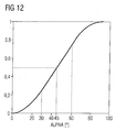
- This antireflection film 30 is formed so as to have a minimum reflection for a predetermined wavelength under a viewing angle ALPHA related to the normal vector N of the surface 14 of the semiconductor layer stack 10, at which the increase of a Zonal flux of the electromagnetic radiation R has approximately a maximum.
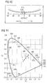
- the course of the zonal light flux is exemplary for a light-emitting diode in FIG. 12 shown in standardized form.
- the illustration is based on a solid angle range between 0 ° and the viewing angle ALPHA.
- the solid angle range starts from the normal vector N and the viewing angle ALPHA can be between 0 ° and 90 °.
- the zonal light flux is normalized to the zonal light flux in a solid angle range between 0 ° and 90 °.
- the maximum increase in the zonal light flux for a value of the viewing angle ALPHA is equal to 45 °. In other words, this means that the highest differential contribution to the total emission of the light-emitting diode is at a solid angle for which the viewing angle ALPHA is equal to 45 °.
- the antireflection layer 30 does not necessarily have to be designed such that for the given wavelength the reflection just below the viewing angle ALPHA related to the normal vector N of the surface 14 is minimal, since the increase of the zonal luminous flux of the electromagnetic radiation R is usually in a wide range is approximately constant by the maximum of the increase of the zonal luminous flux of the electromagnetic radiation R. Therefore, it is sufficient if the antireflection film 30 is formed so that, for the given wavelength of the minimum reflection, a viewing angle ALPHA near to the normal vector N of the surface 14 is sufficient the maximum of the increase in the zonal luminous flux of the electromagnetic radiation R is located.
- the minimum reflection of the antireflection coating 30 is below the viewing angle ALPHA, which is between 30 ° and 60 °, relative to the normal vector N. It is thus possible to achieve a maximization of the total emission for radiation-emitting components 8, for which the maximum of the zonal luminous flux of the electromagnetic radiation R at viewing angles ALPHA is between 30 ° and 60 °.
- the minimum reflection of the antireflection layer 30 for the predetermined wavelength in a range of the viewing angle ALPHA is between 40 ° and 50 °.
- the substrate 18 has a surface 15 which faces away from the semiconductor layer stack 10 ( FIG. 2 ).
- the anti-reflection layer 30 is arranged on the side facing away from the semiconductor layer stack 10 surface 15 of the substrate 18.
- the function of the antireflection layer 30 of the embodiment of FIG. 2 corresponds to the function of the antireflection layer 30 of the embodiment of FIG. 1 ,
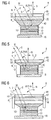
- FIG. 3 1 shows the radiation-emitting component with the semiconductor layer stack 10 and a cover plate 20 spaced from the semiconductor layer stack 10, which has a surface 16 facing the semiconductor layer stack 10 and a surface 17 facing away from the semiconductor layer stack 10.
- the antireflection layer 30 is disposed both on the semiconductor layer stack 10 facing surface 16 and on the side facing away from the semiconductor layer stack 10 surface 17 of the cover plate 20. It can thus be achieved that a minimum reflection is achieved for a given wavelength under a viewing angle ALPHA related to the normal vector N of the surfaces 16, 17, at which the increase in the zonal luminous flux of the electromagnetic radiation R has a maximum. This is particularly advantageous since the minimization of the reflection on both surfaces 16, 17 of the cover plate can thus be achieved.
- the antireflection layer 30 on one or more of the surfaces 14, 15, 16, 17 is made by vapor deposition of one or more thin layers of a material, in particular a metal fluoride or a metal oxide.
- a material in particular a metal fluoride or a metal oxide.
- the metal of the metal fluoride and / or the metal oxide is preferably selected from the group consisting of hafnium, zirconium, aluminum, titanium and magnesium. Suitable materials are in particular magnesium fluoride, silicon dioxide, titanium dioxide or zirconium dioxide.
- the antireflection layer 30 has several layers. This has the advantage that the reflection can be greatly minimized. Furthermore, by forming the antireflection layer 30 of multiple layers, reflection reduction for a plurality of wavelengths can be achieved.
- the radiation-emitting component 8 is preferably formed in other embodiments as a light-emitting diode, which is a mixed light, that is, electromagnetic radiation from at least two wavelength ranges, emitted ( FIGS. 4 to 6 ). Particularly preferred such radiation-emitting components 8 are formed as white light LEDs.
- the radiation-emitting component 8 with the semiconductor layer stack 10 with the active region 12, which is designed to emit an electromagnetic primary radiation P, is shown.
- the radiation-emitting component 8 has a converter layer 40, which is mechanically coupled to the semiconductor layer stack 10.
- the electromagnetic primary radiation P generated when exposed to a current in the forward direction in the active region 12 of the radiation-emitting component 8 may in particular have a spectrum with wavelengths in an ultraviolet to infrared spectral range.
- the spectrum comprises at least one wavelength that is visible to an observer.
- the spectrum of the electromagnetic radiation can advantageously also comprise a plurality of wavelengths, so that a mixed-color luminous impression can arise for a viewer.
- the radiation-emitting component 8 itself to generate electromagnetic primary radiation P having a plurality of wavelengths or for a part of the electromagnetic primary radiation P generated by the radiation-emitting component 8 or for the entire electromagnetic primary radiation P generated by the radiation-emitting component 8 to have a first wavelength , for example in a blue and / or green spectral range, is converted by a wavelength conversion substance into an electromagnetic secondary radiation S of a second wavelength, for example in a yellow and / or red spectral range.
- the active region 12 is followed by the converter layer 40, which has the wavelength conversion substance.
- Suitable wavelength conversion substances and layers with wavelength conversion materials are known to the person skilled in the art with regard to their structure and their function and will not be explained in detail here.
- a portion of the primary electromagnetic radiation P is superimposed with a portion of the secondary electromagnetic radiation S to form an electromagnetic mixed radiation M having a resulting color locus.
- the mixed electromagnetic radiation M is largely white light. It is desirable for such a white-light LED to impart a color impression that is as homogeneous as possible in terms of area.
- the color coordinates C x and C y of the electromagnetic mixed radiation M increase with increasing viewing angle ALPHA. This means that the proportion of secondary electromagnetic radiation S of the second wavelength in the yellow and / or red spectral range in the mixed electromagnetic radiation M increases with increasing viewing angle ALPHA.
- FIG. 11 is a CIE color chart shown with color coordinates or the chromaticity coordinates C x and C y of the electromagnetic mixed radiation M.
- the color location G of the electromagnetic mixed radiation M for a viewing angle ALPHA of 90 ° is entered as well as the color O for a viewing angle ALPHA equal to 0 °.
- Next is the achromatic point E, corresponding to pure white light, in the CIE color chart FIG. 11 specified.
- the cover plate 20 is arranged on the converter layer 40.
- the Cover plate 20 has a surface 17 facing away from the converter layer 40, on which a color correction layer 48 is arranged.
- the color correction layer 48 has at least two adjacently arranged layers 50, 51.
- the first layer 50 consists of a material with a first refractive index N_1
- the second layer 51 consists of a material with a second refractive index N_2.
- the first refractive index N_1 differs from the second refractive index N_2.
- the layers 50, 51 are formed with respect to their refractive indices N_1, N_2 and their thicknesses such that the resulting color locus is adjustable depending on the viewing angle ALPHA.
- the refractive indices N_1, N_2 and the thicknesses of the layers 50, 51 it can be achieved in particular that the color locus G for the viewing angle ALPHA of 90 ° or the color locus O for the viewing angle ALPHA approaches 0 ° closer to the color locus E, as indicated by arrows in the CIE color chart diagram FIG. 11 is indicated.
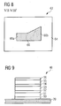
- the color correction layer 48 is formed as a layer stack with a plurality of layers 50, 51, 52, 53, 54, 55, 56, as shown in FIG FIG. 9 is shown schematically, and the layers 50, 51, 52, 53, 54, 55, 56 are arranged so that the two each of the layers adjacent layers have refractive indices, both either smaller or larger than the refractive index of each one layer ,
- one of the layers of the color correction layer 48 is in each case between adjacent layers, which either have both a greater refractive index or a smaller refractive index. It can be a particularly good color correction and thus a particularly far approach of the color G, O at the color point E can be achieved.
- FIG. 5 a modification of the radiation-emitting device 8 is shown, in which the color correction layer 48 is applied directly to a surface 42 of the converter layer 40.
- FIG. 6 shows a modification of the radiation-emitting device 8, in which the cover plate 20 is spaced from the converter layer 40.
- the color correction layer 48 is arranged on the side facing away from the semiconductor layer stack 10 surface 17. This has the advantage that the color correction layer 48 can still be subsequently applied to the cover plate 20. However, the color correction layer 48 can also be arranged additionally or solely on the surface 16 of the cover plate 20 facing the semiconductor layer stack 10.
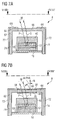
- FIGS. 7A and 7B show modifications of the radiation-emitting component 8 with the semiconductor layer stack 10 with the active region 12.
- the semiconductor layer stack 10 is designed to emit electromagnetic primary radiation P.
- the radiation-emitting component 8 has the converter layer 40, which is mechanically coupled to the semiconductor layer stack 10.
- the converter layer 40 with a phosphor is designed to convert part of the primary electromagnetic radiation P into the secondary electromagnetic radiation S. A portion of the primary electromagnetic radiation P and the secondary electromagnetic radiation S overlap to form the mixed radiation N with the resulting color locus.
- the radiation-emitting device 8 has a cover member 62 having a first portion 64 and a second portion 66.
- the cover member 62 has an outer surface 68 and an inner surface 70.
- On the outer surface 68 of the first portion 64 of the cover member 62 is an absorbent or reflective Layer 72 arranged.
- the surface 68, 70 of the second portion 66 of the cover member 62 is free of the absorbent or reflective layer 72.
- the reflective and / or absorbing layer 72 may in particular also be arranged on side sections 74 of the cover element 62.
- a transmission of light in particular in the side portions 74 of the cover member 62 and in parts of the front portion of the first portion 64 of the cover member 62 near the second portion 66 of the cover member 62 (see FIG. 8 ) be avoided.
- the second portion 66 of the cover member 62 which is free of the absorbing and / or reflecting layer 72, may have a suitable shape as shown in FIG FIG. 8 is shown. If the radiation-emitting component 8 is to be used, for example, for a headlight of a motor vehicle, then the light cone has a more or less abrupt dark / light transition at the transition from the first portion 64 to the second portion 66.
- the second portion 66 of the cover member 62 may have two sections 66a, 66b, the main directions of extension of which are inclined relative to each other, such that they enclose an angle of approximately 150 ° to 170 ° with each other. This is particularly advantageous when the second portion 66 of the cover 62 as a shutter element for a headlight a motor vehicle is to be used, and the shutter element is preferably to be used as asymmetric low beam.
- FIG. 7B shows the radiation-emitting component 8, wherein on the surface 68 of the second portion 66 of the cover 62, an anti-reflection layer 58 is arranged.
- the anti-reflection layer 58 is formed such that the radiation-emitting device 8 has a minimum reflection under a viewing angle ALPHA related to the normal vector N of the surface 68, 70 at which the increase of the zonal luminous flux of the mixed electromagnetic radiation M is approximately a maximum having.
- the antireflection film 58 is preferably formed to have minimum reflection for the predetermined wavelength at the viewing angle ALPHA between 40 and 50 °. It is particularly preferred if the antireflection layer 58 is formed from a metal fluoride or a metal oxide.
- the metal is selected from the group of hafnium, zirconium, aluminum, titanium and magnesium.
- the color correction layer 48 On the surface 70 of the second portion 66 of the cover member 62, the color correction layer 48 is arranged.
- the color correction layer 48 has at least two adjacently arranged layers 50, 51.
- the first layer 50 consists of a material with a first refractive index N_1 and the second layer 51 consists of a material with a second refractive index N_2.
- the first refractive index N_1 is different from the second refractive index N_2.
- the color correction layer 48 may be used as a layer stack be formed with a plurality of layers 50, 51, 52, 53, 54, 55, 56 ( FIG. 9 ).
- the antireflection layer 58 and the color correction layer 48 are disposed on the two oppositely disposed surfaces 68, 70 of the second portion 66 of the cover member 62.
- the second portion 66 of the cover member 62 may serve to receive both the anti-reflection layer 58 and the color correction layer 48.
Landscapes
- Led Device Packages (AREA)
- Led Devices (AREA)
Applications Claiming Priority (3)
| Application Number | Priority Date | Filing Date | Title |
|---|---|---|---|
| DE102007045087 | 2007-09-21 | ||
| DE102008005344A DE102008005344A1 (de) | 2007-09-21 | 2008-01-21 | Strahlungsemittierendes Bauelement |
| PCT/DE2008/001448 WO2009036731A2 (de) | 2007-09-21 | 2008-08-28 | Strahlungsemittierendes bauelement |
Publications (2)
| Publication Number | Publication Date |
|---|---|
| EP2198464A2 EP2198464A2 (de) | 2010-06-23 |
| EP2198464B1 true EP2198464B1 (de) | 2016-11-16 |
Family
ID=40384494
Family Applications (1)
| Application Number | Title | Priority Date | Filing Date |
|---|---|---|---|
| EP08801255.4A Not-in-force EP2198464B1 (de) | 2007-09-21 | 2008-08-28 | Strahlungsemittierendes bauelement |
Country Status (8)
| Country | Link |
|---|---|
| US (2) | US8373186B2 (enExample) |
| EP (1) | EP2198464B1 (enExample) |
| JP (1) | JP5362727B2 (enExample) |
| KR (1) | KR101460388B1 (enExample) |
| CN (2) | CN102347417B (enExample) |
| DE (1) | DE102008005344A1 (enExample) |
| TW (2) | TW200915624A (enExample) |
| WO (1) | WO2009036731A2 (enExample) |
Families Citing this family (7)
| Publication number | Priority date | Publication date | Assignee | Title |
|---|---|---|---|---|
| DE102012100788A1 (de) * | 2012-01-31 | 2013-08-01 | Osram Opto Semiconductors Gmbh | Optoelektronisches Halbleiterbauelement mit Konverterelement |
| CN103633223B (zh) * | 2013-11-13 | 2016-08-17 | 苏州热驰光电科技有限公司 | 高光透玻璃基板led照明装置及其制备方法 |
| CA2967190C (en) * | 2014-11-18 | 2022-09-20 | Industries Yifei Wang Inc. | Led module, methods of manufacturing same and luminaire integrating same |
| DE112020002375A5 (de) * | 2019-05-14 | 2022-01-27 | OSRAM Opto Semiconductors Gesellschaft mit beschränkter Haftung | Optoelektronisches bauelement, pixel, displayanordnung und verfahren |
| KR20240133228A (ko) * | 2023-02-28 | 2024-09-04 | 삼성전자주식회사 | 반도체 발광 소자 |
| CN116344707A (zh) * | 2023-03-20 | 2023-06-27 | 华灿光电(浙江)有限公司 | 改善发光亮度的发光二极管及其制备方法 |
| CN120214069B (zh) * | 2025-05-23 | 2025-08-22 | 上海聚跃检测技术有限公司 | 一种半导体晶圆表面的芯片检测方法及系统 |
Family Cites Families (19)
| Publication number | Priority date | Publication date | Assignee | Title |
|---|---|---|---|---|
| JPH11145519A (ja) * | 1997-09-02 | 1999-05-28 | Toshiba Corp | 半導体発光素子、半導体発光装置および画像表示装置 |
| EP1277240B1 (de) * | 2000-04-26 | 2015-05-20 | OSRAM Opto Semiconductors GmbH | Verfahren zur Herstellung eines lichtmittierenden Halbleiterbauelements |
| US20020017652A1 (en) * | 2000-08-08 | 2002-02-14 | Stefan Illek | Semiconductor chip for optoelectronics |
| US7075112B2 (en) * | 2001-01-31 | 2006-07-11 | Gentex Corporation | High power radiation emitter device and heat dissipating package for electronic components |
| US6630689B2 (en) * | 2001-05-09 | 2003-10-07 | Lumileds Lighting, U.S. Llc | Semiconductor LED flip-chip with high reflectivity dielectric coating on the mesa |
| US6455878B1 (en) * | 2001-05-15 | 2002-09-24 | Lumileds Lighting U.S., Llc | Semiconductor LED flip-chip having low refractive index underfill |
| KR101280003B1 (ko) | 2002-12-25 | 2013-07-05 | 도꾸리쯔교세이호징 가가꾸 기쥬쯔 신꼬 기꼬 | 발광소자장치, 수광소자장치, 광학장치, 플루오르화물 결정, 플루오르화물 결정의 제조방법 및 도가니 |
| US7087936B2 (en) * | 2003-04-30 | 2006-08-08 | Cree, Inc. | Methods of forming light-emitting devices having an antireflective layer that has a graded index of refraction |
| JP2005157313A (ja) * | 2003-10-30 | 2005-06-16 | Arisawa Mfg Co Ltd | リアプロジェクションディスプレイ用スクリーン |
| FR2861853B1 (fr) | 2003-10-30 | 2006-02-24 | Soitec Silicon On Insulator | Substrat avec adaptation d'indice |
| TW200602585A (en) | 2004-03-16 | 2006-01-16 | Koninkl Philips Electronics Nv | High brightness illumination device with incoherent solid state light source |
| JP2006093602A (ja) | 2004-09-27 | 2006-04-06 | Toyoda Gosei Co Ltd | 発光素子 |
| DE102004047640A1 (de) * | 2004-09-30 | 2006-04-13 | Osram Opto Semiconductors Gmbh | Optoelektronisches Bauelement und Gehäuse für ein optoelektronisches Bauelement |
| DE102004047727B4 (de) * | 2004-09-30 | 2018-01-18 | Osram Opto Semiconductors Gmbh | Lumineszenzdiodenchip mit einer Konverterschicht und Verfahren zur Herstellung eines Lumineszenzdiodenchips mit einer Konverterschicht |
| DE602005023891D1 (de) * | 2004-10-12 | 2010-11-11 | Philips Intellectual Property | Elektroluminsezente lichtquelle |
| TWI239671B (en) * | 2004-12-30 | 2005-09-11 | Ind Tech Res Inst | LED applied with omnidirectional reflector |
| US7341878B2 (en) * | 2005-03-14 | 2008-03-11 | Philips Lumileds Lighting Company, Llc | Wavelength-converted semiconductor light emitting device |
| JP2006261540A (ja) | 2005-03-18 | 2006-09-28 | Stanley Electric Co Ltd | 発光デバイス |
| JP4996101B2 (ja) * | 2006-02-02 | 2012-08-08 | 新光電気工業株式会社 | 半導体装置及び半導体装置の製造方法 |
-
2008
- 2008-01-21 DE DE102008005344A patent/DE102008005344A1/de not_active Withdrawn
- 2008-08-18 TW TW097131452A patent/TW200915624A/zh unknown
- 2008-08-18 TW TW101124292A patent/TWI473297B/zh not_active IP Right Cessation
- 2008-08-28 CN CN201110340389.0A patent/CN102347417B/zh not_active Expired - Fee Related
- 2008-08-28 WO PCT/DE2008/001448 patent/WO2009036731A2/de not_active Ceased
- 2008-08-28 CN CN2008801079846A patent/CN101803048B/zh not_active Expired - Fee Related
- 2008-08-28 JP JP2010525192A patent/JP5362727B2/ja not_active Expired - Fee Related
- 2008-08-28 EP EP08801255.4A patent/EP2198464B1/de not_active Not-in-force
- 2008-08-28 US US12/677,320 patent/US8373186B2/en not_active Expired - Fee Related
- 2008-08-28 KR KR1020097025704A patent/KR101460388B1/ko not_active Expired - Fee Related
-
2012
- 2012-12-12 US US13/711,662 patent/US8963181B2/en not_active Expired - Fee Related
Also Published As
| Publication number | Publication date |
|---|---|
| TW200915624A (en) | 2009-04-01 |
| KR101460388B1 (ko) | 2014-11-10 |
| CN102347417B (zh) | 2014-10-01 |
| CN102347417A (zh) | 2012-02-08 |
| WO2009036731A2 (de) | 2009-03-26 |
| WO2009036731A3 (de) | 2009-05-28 |
| US8963181B2 (en) | 2015-02-24 |
| EP2198464A2 (de) | 2010-06-23 |
| CN101803048B (zh) | 2011-12-21 |
| CN101803048A (zh) | 2010-08-11 |
| US20100207148A1 (en) | 2010-08-19 |
| JP5362727B2 (ja) | 2013-12-11 |
| US20130146919A1 (en) | 2013-06-13 |
| TW201242078A (en) | 2012-10-16 |
| DE102008005344A1 (de) | 2009-04-02 |
| US8373186B2 (en) | 2013-02-12 |
| JP2010539715A (ja) | 2010-12-16 |
| TWI473297B (zh) | 2015-02-11 |
| KR20100055357A (ko) | 2010-05-26 |
Similar Documents
| Publication | Publication Date | Title |
|---|---|---|
| EP2561386B1 (de) | Flächenlichtleiter und flächenstrahler | |
| EP2198464B1 (de) | Strahlungsemittierendes bauelement | |
| EP2149163B9 (de) | Lumineszenzdiodenchip mit winkelfilterelement | |
| DE102011012297B4 (de) | Beleuchtungsvorrichtung | |
| DE102010018033A1 (de) | Flächenlichtleiter und Flächenstrahler | |
| EP2054948A1 (de) | Optoelektronisches bauelement | |
| DE102012106943B4 (de) | Verfahren zur Herstellung einer Halbleiterlaserdiode und Halbleiterlaserdiode | |
| EP2067177B1 (de) | Optoelektronisches bauelement | |
| EP3378105B1 (de) | Halbleiterbauelement | |
| WO2011144385A1 (de) | Optoelektronisches halbleiterbauteil und verfahren zur herstellung einer abdeckschicht | |
| WO2005100016A2 (de) | Lichtemittierendes paneel und optisch wirksame folie | |
| EP2193561A1 (de) | Optoelektronisches bauteil | |
| DE102007044597A1 (de) | Optoelektronisches Bauteil | |
| DE102016104616A1 (de) | Halbleiterlichtquelle | |
| WO2021204654A1 (de) | Optoelektronisches bauelement | |
| DE102015101573A1 (de) | Konversionselement und optoelektronisches Bauelement | |
| DE102016104602A1 (de) | Halbleiterlichtquelle | |
| WO2021204653A1 (de) | Halbleiterbauelement und verfahren zur herstellung eines halbleiterbauelements | |
| WO2014048797A2 (de) | Ringlichtmodul und verfahren zur herstellung eines ringlichtmoduls | |
| DE112020001069T5 (de) | Optoelektronische halbleiterlichtquelle und bragg-spiegel | |
| WO2021204652A1 (de) | Optoelektronisches bauelement und beleuchtungsvorrichtung | |
| DE102013102967A1 (de) | Beleuchtungsmodul mit Lichtleitkörper und Verfahren zum Herstellen eines Beleuchtungsmoduls | |
| EP2764554B1 (de) | Optoelektronisches halbleiterbauelement und modul mit einer mehrzahl von derartigen bauelementen | |
| WO2021204511A1 (de) | Strahlungsemittierende vorrichtung und projektor damit | |
| DE102021134547A1 (de) | Laserbauteil |
Legal Events
| Date | Code | Title | Description |
|---|---|---|---|
| PUAI | Public reference made under article 153(3) epc to a published international application that has entered the european phase |
Free format text: ORIGINAL CODE: 0009012 |
|
| 17P | Request for examination filed |
Effective date: 20090921 |
|
| AK | Designated contracting states |
Kind code of ref document: A2 Designated state(s): AT BE BG CH CY CZ DE DK EE ES FI FR GB GR HR HU IE IS IT LI LT LU LV MC MT NL NO PL PT RO SE SI SK TR |
|
| AX | Request for extension of the european patent |
Extension state: AL BA MK RS |
|
| DAX | Request for extension of the european patent (deleted) | ||
| REG | Reference to a national code |
Ref country code: DE Ref legal event code: R079 Ref document number: 502008014807 Country of ref document: DE Free format text: PREVIOUS MAIN CLASS: H01L0033000000 Ipc: H01L0033440000 |
|
| GRAP | Despatch of communication of intention to grant a patent |
Free format text: ORIGINAL CODE: EPIDOSNIGR1 |
|
| RIC1 | Information provided on ipc code assigned before grant |
Ipc: H01L 33/44 20100101AFI20160512BHEP |
|
| INTG | Intention to grant announced |
Effective date: 20160616 |
|
| GRAS | Grant fee paid |
Free format text: ORIGINAL CODE: EPIDOSNIGR3 |
|
| GRAA | (expected) grant |
Free format text: ORIGINAL CODE: 0009210 |
|
| AK | Designated contracting states |
Kind code of ref document: B1 Designated state(s): AT BE BG CH CY CZ DE DK EE ES FI FR GB GR HR HU IE IS IT LI LT LU LV MC MT NL NO PL PT RO SE SI SK TR |
|
| REG | Reference to a national code |
Ref country code: GB Ref legal event code: FG4D Free format text: NOT ENGLISH |
|
| REG | Reference to a national code |
Ref country code: CH Ref legal event code: EP |
|
| REG | Reference to a national code |
Ref country code: IE Ref legal event code: FG4D Free format text: LANGUAGE OF EP DOCUMENT: GERMAN |
|
| REG | Reference to a national code |
Ref country code: AT Ref legal event code: REF Ref document number: 846659 Country of ref document: AT Kind code of ref document: T Effective date: 20161215 |
|
| REG | Reference to a national code |
Ref country code: DE Ref legal event code: R096 Ref document number: 502008014807 Country of ref document: DE |
|
| PG25 | Lapsed in a contracting state [announced via postgrant information from national office to epo] |
Ref country code: LV Free format text: LAPSE BECAUSE OF FAILURE TO SUBMIT A TRANSLATION OF THE DESCRIPTION OR TO PAY THE FEE WITHIN THE PRESCRIBED TIME-LIMIT Effective date: 20161116 |
|
| REG | Reference to a national code |
Ref country code: NL Ref legal event code: MP Effective date: 20161116 |
|
| REG | Reference to a national code |
Ref country code: LT Ref legal event code: MG4D |
|
| PG25 | Lapsed in a contracting state [announced via postgrant information from national office to epo] |
Ref country code: NO Free format text: LAPSE BECAUSE OF FAILURE TO SUBMIT A TRANSLATION OF THE DESCRIPTION OR TO PAY THE FEE WITHIN THE PRESCRIBED TIME-LIMIT Effective date: 20170216 Ref country code: NL Free format text: LAPSE BECAUSE OF FAILURE TO SUBMIT A TRANSLATION OF THE DESCRIPTION OR TO PAY THE FEE WITHIN THE PRESCRIBED TIME-LIMIT Effective date: 20161116 Ref country code: SE Free format text: LAPSE BECAUSE OF FAILURE TO SUBMIT A TRANSLATION OF THE DESCRIPTION OR TO PAY THE FEE WITHIN THE PRESCRIBED TIME-LIMIT Effective date: 20161116 Ref country code: LT Free format text: LAPSE BECAUSE OF FAILURE TO SUBMIT A TRANSLATION OF THE DESCRIPTION OR TO PAY THE FEE WITHIN THE PRESCRIBED TIME-LIMIT Effective date: 20161116 Ref country code: GR Free format text: LAPSE BECAUSE OF FAILURE TO SUBMIT A TRANSLATION OF THE DESCRIPTION OR TO PAY THE FEE WITHIN THE PRESCRIBED TIME-LIMIT Effective date: 20170217 |
|
| PG25 | Lapsed in a contracting state [announced via postgrant information from national office to epo] |
Ref country code: HR Free format text: LAPSE BECAUSE OF FAILURE TO SUBMIT A TRANSLATION OF THE DESCRIPTION OR TO PAY THE FEE WITHIN THE PRESCRIBED TIME-LIMIT Effective date: 20161116 Ref country code: PL Free format text: LAPSE BECAUSE OF FAILURE TO SUBMIT A TRANSLATION OF THE DESCRIPTION OR TO PAY THE FEE WITHIN THE PRESCRIBED TIME-LIMIT Effective date: 20161116 Ref country code: ES Free format text: LAPSE BECAUSE OF FAILURE TO SUBMIT A TRANSLATION OF THE DESCRIPTION OR TO PAY THE FEE WITHIN THE PRESCRIBED TIME-LIMIT Effective date: 20161116 Ref country code: FI Free format text: LAPSE BECAUSE OF FAILURE TO SUBMIT A TRANSLATION OF THE DESCRIPTION OR TO PAY THE FEE WITHIN THE PRESCRIBED TIME-LIMIT Effective date: 20161116 Ref country code: PT Free format text: LAPSE BECAUSE OF FAILURE TO SUBMIT A TRANSLATION OF THE DESCRIPTION OR TO PAY THE FEE WITHIN THE PRESCRIBED TIME-LIMIT Effective date: 20170316 |
|
| PG25 | Lapsed in a contracting state [announced via postgrant information from national office to epo] |
Ref country code: SK Free format text: LAPSE BECAUSE OF FAILURE TO SUBMIT A TRANSLATION OF THE DESCRIPTION OR TO PAY THE FEE WITHIN THE PRESCRIBED TIME-LIMIT Effective date: 20161116 Ref country code: EE Free format text: LAPSE BECAUSE OF FAILURE TO SUBMIT A TRANSLATION OF THE DESCRIPTION OR TO PAY THE FEE WITHIN THE PRESCRIBED TIME-LIMIT Effective date: 20161116 Ref country code: RO Free format text: LAPSE BECAUSE OF FAILURE TO SUBMIT A TRANSLATION OF THE DESCRIPTION OR TO PAY THE FEE WITHIN THE PRESCRIBED TIME-LIMIT Effective date: 20161116 Ref country code: CZ Free format text: LAPSE BECAUSE OF FAILURE TO SUBMIT A TRANSLATION OF THE DESCRIPTION OR TO PAY THE FEE WITHIN THE PRESCRIBED TIME-LIMIT Effective date: 20161116 Ref country code: DK Free format text: LAPSE BECAUSE OF FAILURE TO SUBMIT A TRANSLATION OF THE DESCRIPTION OR TO PAY THE FEE WITHIN THE PRESCRIBED TIME-LIMIT Effective date: 20161116 |
|
| REG | Reference to a national code |
Ref country code: DE Ref legal event code: R097 Ref document number: 502008014807 Country of ref document: DE |
|
| PG25 | Lapsed in a contracting state [announced via postgrant information from national office to epo] |
Ref country code: BG Free format text: LAPSE BECAUSE OF FAILURE TO SUBMIT A TRANSLATION OF THE DESCRIPTION OR TO PAY THE FEE WITHIN THE PRESCRIBED TIME-LIMIT Effective date: 20170216 Ref country code: IT Free format text: LAPSE BECAUSE OF FAILURE TO SUBMIT A TRANSLATION OF THE DESCRIPTION OR TO PAY THE FEE WITHIN THE PRESCRIBED TIME-LIMIT Effective date: 20161116 |
|
| PLBE | No opposition filed within time limit |
Free format text: ORIGINAL CODE: 0009261 |
|
| STAA | Information on the status of an ep patent application or granted ep patent |
Free format text: STATUS: NO OPPOSITION FILED WITHIN TIME LIMIT |
|
| 26N | No opposition filed |
Effective date: 20170817 |
|
| PG25 | Lapsed in a contracting state [announced via postgrant information from national office to epo] |
Ref country code: SI Free format text: LAPSE BECAUSE OF FAILURE TO SUBMIT A TRANSLATION OF THE DESCRIPTION OR TO PAY THE FEE WITHIN THE PRESCRIBED TIME-LIMIT Effective date: 20161116 |
|
| REG | Reference to a national code |
Ref country code: CH Ref legal event code: PL |
|
| PG25 | Lapsed in a contracting state [announced via postgrant information from national office to epo] |
Ref country code: MC Free format text: LAPSE BECAUSE OF FAILURE TO SUBMIT A TRANSLATION OF THE DESCRIPTION OR TO PAY THE FEE WITHIN THE PRESCRIBED TIME-LIMIT Effective date: 20161116 |
|
| GBPC | Gb: european patent ceased through non-payment of renewal fee |
Effective date: 20170828 |
|
| PG25 | Lapsed in a contracting state [announced via postgrant information from national office to epo] |
Ref country code: CH Free format text: LAPSE BECAUSE OF NON-PAYMENT OF DUE FEES Effective date: 20170831 Ref country code: LI Free format text: LAPSE BECAUSE OF NON-PAYMENT OF DUE FEES Effective date: 20170831 |
|
| REG | Reference to a national code |
Ref country code: FR Ref legal event code: ST Effective date: 20180430 |
|
| REG | Reference to a national code |
Ref country code: IE Ref legal event code: MM4A |
|
| REG | Reference to a national code |
Ref country code: BE Ref legal event code: MM Effective date: 20170831 |
|
| PG25 | Lapsed in a contracting state [announced via postgrant information from national office to epo] |
Ref country code: LU Free format text: LAPSE BECAUSE OF NON-PAYMENT OF DUE FEES Effective date: 20170828 |
|
| PG25 | Lapsed in a contracting state [announced via postgrant information from national office to epo] |
Ref country code: IE Free format text: LAPSE BECAUSE OF NON-PAYMENT OF DUE FEES Effective date: 20170828 Ref country code: GB Free format text: LAPSE BECAUSE OF NON-PAYMENT OF DUE FEES Effective date: 20170828 |
|
| PG25 | Lapsed in a contracting state [announced via postgrant information from national office to epo] |
Ref country code: FR Free format text: LAPSE BECAUSE OF NON-PAYMENT OF DUE FEES Effective date: 20170831 Ref country code: BE Free format text: LAPSE BECAUSE OF NON-PAYMENT OF DUE FEES Effective date: 20170831 |
|
| PG25 | Lapsed in a contracting state [announced via postgrant information from national office to epo] |
Ref country code: MT Free format text: LAPSE BECAUSE OF FAILURE TO SUBMIT A TRANSLATION OF THE DESCRIPTION OR TO PAY THE FEE WITHIN THE PRESCRIBED TIME-LIMIT Effective date: 20161116 |
|
| REG | Reference to a national code |
Ref country code: AT Ref legal event code: MM01 Ref document number: 846659 Country of ref document: AT Kind code of ref document: T Effective date: 20170828 |
|
| PGFP | Annual fee paid to national office [announced via postgrant information from national office to epo] |
Ref country code: DE Payment date: 20180823 Year of fee payment: 11 |
|
| PG25 | Lapsed in a contracting state [announced via postgrant information from national office to epo] |
Ref country code: AT Free format text: LAPSE BECAUSE OF NON-PAYMENT OF DUE FEES Effective date: 20170828 |
|
| PG25 | Lapsed in a contracting state [announced via postgrant information from national office to epo] |
Ref country code: HU Free format text: LAPSE BECAUSE OF FAILURE TO SUBMIT A TRANSLATION OF THE DESCRIPTION OR TO PAY THE FEE WITHIN THE PRESCRIBED TIME-LIMIT; INVALID AB INITIO Effective date: 20080828 |
|
| PG25 | Lapsed in a contracting state [announced via postgrant information from national office to epo] |
Ref country code: CY Free format text: LAPSE BECAUSE OF NON-PAYMENT OF DUE FEES Effective date: 20161116 |
|
| REG | Reference to a national code |
Ref country code: DE Ref legal event code: R119 Ref document number: 502008014807 Country of ref document: DE |
|
| PG25 | Lapsed in a contracting state [announced via postgrant information from national office to epo] |
Ref country code: TR Free format text: LAPSE BECAUSE OF FAILURE TO SUBMIT A TRANSLATION OF THE DESCRIPTION OR TO PAY THE FEE WITHIN THE PRESCRIBED TIME-LIMIT Effective date: 20161116 |
|
| PG25 | Lapsed in a contracting state [announced via postgrant information from national office to epo] |
Ref country code: DE Free format text: LAPSE BECAUSE OF NON-PAYMENT OF DUE FEES Effective date: 20200303 Ref country code: IS Free format text: LAPSE BECAUSE OF FAILURE TO SUBMIT A TRANSLATION OF THE DESCRIPTION OR TO PAY THE FEE WITHIN THE PRESCRIBED TIME-LIMIT Effective date: 20170316 |