EP2180532A2 - Semiconductor light emitting device - Google Patents
Semiconductor light emitting device Download PDFInfo
- Publication number
- EP2180532A2 EP2180532A2 EP09013440A EP09013440A EP2180532A2 EP 2180532 A2 EP2180532 A2 EP 2180532A2 EP 09013440 A EP09013440 A EP 09013440A EP 09013440 A EP09013440 A EP 09013440A EP 2180532 A2 EP2180532 A2 EP 2180532A2
- Authority
- EP
- European Patent Office
- Prior art keywords
- layer
- light emitting
- electrode
- conductive semiconductor
- emitting device
- Prior art date
- Legal status (The legal status is an assumption and is not a legal conclusion. Google has not performed a legal analysis and makes no representation as to the accuracy of the status listed.)
- Granted
Links
- 239000004065 semiconductor Substances 0.000 title claims abstract description 197
- 229910052751 metal Inorganic materials 0.000 claims abstract description 43
- 239000002184 metal Substances 0.000 claims abstract description 43
- 150000001875 compounds Chemical class 0.000 claims abstract description 20
- 239000000463 material Substances 0.000 claims description 19
- 229910052737 gold Inorganic materials 0.000 claims description 16
- 229910052759 nickel Inorganic materials 0.000 claims description 14
- 229910052738 indium Inorganic materials 0.000 claims description 6
- 229910052710 silicon Inorganic materials 0.000 claims description 6
- 229910045601 alloy Inorganic materials 0.000 claims description 3
- 239000000956 alloy Substances 0.000 claims description 3
- 239000010410 layer Substances 0.000 description 331
- 239000010931 gold Substances 0.000 description 19
- PXHVJJICTQNCMI-UHFFFAOYSA-N nickel Substances [Ni] PXHVJJICTQNCMI-UHFFFAOYSA-N 0.000 description 19
- 239000000758 substrate Substances 0.000 description 19
- 238000000034 method Methods 0.000 description 16
- VYPSYNLAJGMNEJ-UHFFFAOYSA-N Silicium dioxide Chemical compound O=[Si]=O VYPSYNLAJGMNEJ-UHFFFAOYSA-N 0.000 description 15
- 239000010949 copper Substances 0.000 description 12
- 239000002019 doping agent Substances 0.000 description 12
- 239000003990 capacitor Substances 0.000 description 11
- 239000010936 titanium Substances 0.000 description 11
- 229910052719 titanium Inorganic materials 0.000 description 9
- 229910052804 chromium Inorganic materials 0.000 description 8
- 229910052802 copper Inorganic materials 0.000 description 8
- 229910001218 Gallium arsenide Inorganic materials 0.000 description 7
- 229910002704 AlGaN Inorganic materials 0.000 description 6
- VRIVJOXICYMTAG-IYEMJOQQSA-L iron(ii) gluconate Chemical compound [Fe+2].OC[C@@H](O)[C@@H](O)[C@H](O)[C@@H](O)C([O-])=O.OC[C@@H](O)[C@@H](O)[C@H](O)[C@@H](O)C([O-])=O VRIVJOXICYMTAG-IYEMJOQQSA-L 0.000 description 6
- 229910052715 tantalum Inorganic materials 0.000 description 6
- 229910052581 Si3N4 Inorganic materials 0.000 description 5
- 229910020286 SiOxNy Inorganic materials 0.000 description 5
- 229910052681 coesite Inorganic materials 0.000 description 5
- 229910052906 cristobalite Inorganic materials 0.000 description 5
- 239000000377 silicon dioxide Substances 0.000 description 5
- 229910052814 silicon oxide Inorganic materials 0.000 description 5
- 229910052682 stishovite Inorganic materials 0.000 description 5
- 229910052905 tridymite Inorganic materials 0.000 description 5
- 229910000980 Aluminium gallium arsenide Inorganic materials 0.000 description 4
- 229910005540 GaP Inorganic materials 0.000 description 4
- 229910019897 RuOx Inorganic materials 0.000 description 4
- GWEVSGVZZGPLCZ-UHFFFAOYSA-N Titan oxide Chemical compound O=[Ti]=O GWEVSGVZZGPLCZ-UHFFFAOYSA-N 0.000 description 4
- 239000000853 adhesive Substances 0.000 description 4
- 230000001070 adhesive effect Effects 0.000 description 4
- 239000012790 adhesive layer Substances 0.000 description 4
- 230000004888 barrier function Effects 0.000 description 4
- 238000010586 diagram Methods 0.000 description 4
- 238000004519 manufacturing process Methods 0.000 description 4
- 229910052763 palladium Inorganic materials 0.000 description 4
- 229910052697 platinum Inorganic materials 0.000 description 4
- 229910052709 silver Inorganic materials 0.000 description 4
- 239000000126 substance Substances 0.000 description 4
- 229910052718 tin Inorganic materials 0.000 description 4
- 229910052725 zinc Inorganic materials 0.000 description 4
- PNEYBMLMFCGWSK-UHFFFAOYSA-N aluminium oxide Inorganic materials [O-2].[O-2].[O-2].[Al+3].[Al+3] PNEYBMLMFCGWSK-UHFFFAOYSA-N 0.000 description 3
- 238000005229 chemical vapour deposition Methods 0.000 description 3
- 229910052593 corundum Inorganic materials 0.000 description 3
- 238000012986 modification Methods 0.000 description 3
- 230000004048 modification Effects 0.000 description 3
- 150000004767 nitrides Chemical class 0.000 description 3
- 229910001845 yogo sapphire Inorganic materials 0.000 description 3
- RYGMFSIKBFXOCR-UHFFFAOYSA-N Copper Chemical compound [Cu] RYGMFSIKBFXOCR-UHFFFAOYSA-N 0.000 description 2
- ZOKXTWBITQBERF-UHFFFAOYSA-N Molybdenum Chemical compound [Mo] ZOKXTWBITQBERF-UHFFFAOYSA-N 0.000 description 2
- 229910000577 Silicon-germanium Inorganic materials 0.000 description 2
- 230000002159 abnormal effect Effects 0.000 description 2
- 229910052782 aluminium Inorganic materials 0.000 description 2
- 229910052797 bismuth Inorganic materials 0.000 description 2
- 239000011651 chromium Substances 0.000 description 2
- SBYXRAKIOMOBFF-UHFFFAOYSA-N copper tungsten Chemical compound [Cu].[W] SBYXRAKIOMOBFF-UHFFFAOYSA-N 0.000 description 2
- 238000009713 electroplating Methods 0.000 description 2
- 238000005530 etching Methods 0.000 description 2
- 229910052733 gallium Inorganic materials 0.000 description 2
- PCHJSUWPFVWCPO-UHFFFAOYSA-N gold Chemical compound [Au] PCHJSUWPFVWCPO-UHFFFAOYSA-N 0.000 description 2
- 229910021476 group 6 element Inorganic materials 0.000 description 2
- 229910052735 hafnium Inorganic materials 0.000 description 2
- 238000009616 inductively coupled plasma Methods 0.000 description 2
- 239000011810 insulating material Substances 0.000 description 2
- 229910052741 iridium Inorganic materials 0.000 description 2
- 238000002955 isolation Methods 0.000 description 2
- 239000007769 metal material Substances 0.000 description 2
- 229910052750 molybdenum Inorganic materials 0.000 description 2
- 239000011733 molybdenum Substances 0.000 description 2
- KDLHZDBZIXYQEI-UHFFFAOYSA-N palladium Substances [Pd] KDLHZDBZIXYQEI-UHFFFAOYSA-N 0.000 description 2
- 238000005240 physical vapour deposition Methods 0.000 description 2
- 238000001020 plasma etching Methods 0.000 description 2
- 238000007747 plating Methods 0.000 description 2
- BASFCYQUMIYNBI-UHFFFAOYSA-N platinum Substances [Pt] BASFCYQUMIYNBI-UHFFFAOYSA-N 0.000 description 2
- 229910052703 rhodium Inorganic materials 0.000 description 2
- 239000010948 rhodium Substances 0.000 description 2
- 238000000926 separation method Methods 0.000 description 2
- 239000011135 tin Substances 0.000 description 2
- 239000011162 core material Substances 0.000 description 1
- 230000007547 defect Effects 0.000 description 1
- 230000032798 delamination Effects 0.000 description 1
- 238000000151 deposition Methods 0.000 description 1
- 230000008021 deposition Effects 0.000 description 1
- 230000000694 effects Effects 0.000 description 1
- 230000005611 electricity Effects 0.000 description 1
- 238000010894 electron beam technology Methods 0.000 description 1
- QZQVBEXLDFYHSR-UHFFFAOYSA-N gallium(III) oxide Inorganic materials O=[Ga]O[Ga]=O QZQVBEXLDFYHSR-UHFFFAOYSA-N 0.000 description 1
- 238000005286 illumination Methods 0.000 description 1
- 239000011229 interlayer Substances 0.000 description 1
- 230000001678 irradiating effect Effects 0.000 description 1
- 238000007517 polishing process Methods 0.000 description 1
- 229910052594 sapphire Inorganic materials 0.000 description 1
- 239000010980 sapphire Substances 0.000 description 1
- 238000004544 sputter deposition Methods 0.000 description 1
Images


Classifications
-
- H—ELECTRICITY
- H01—ELECTRIC ELEMENTS
- H01L—SEMICONDUCTOR DEVICES NOT COVERED BY CLASS H10
- H01L33/00—Semiconductor devices with at least one potential-jump barrier or surface barrier specially adapted for light emission; Processes or apparatus specially adapted for the manufacture or treatment thereof or of parts thereof; Details thereof
- H01L33/36—Semiconductor devices with at least one potential-jump barrier or surface barrier specially adapted for light emission; Processes or apparatus specially adapted for the manufacture or treatment thereof or of parts thereof; Details thereof characterised by the electrodes
- H01L33/38—Semiconductor devices with at least one potential-jump barrier or surface barrier specially adapted for light emission; Processes or apparatus specially adapted for the manufacture or treatment thereof or of parts thereof; Details thereof characterised by the electrodes with a particular shape
- H01L33/385—Semiconductor devices with at least one potential-jump barrier or surface barrier specially adapted for light emission; Processes or apparatus specially adapted for the manufacture or treatment thereof or of parts thereof; Details thereof characterised by the electrodes with a particular shape the electrode extending at least partially onto a side surface of the semiconductor body
-
- H—ELECTRICITY
- H01—ELECTRIC ELEMENTS
- H01L—SEMICONDUCTOR DEVICES NOT COVERED BY CLASS H10
- H01L25/00—Assemblies consisting of a plurality of individual semiconductor or other solid state devices ; Multistep manufacturing processes thereof
- H01L25/16—Assemblies consisting of a plurality of individual semiconductor or other solid state devices ; Multistep manufacturing processes thereof the devices being of types provided for in two or more different main groups of groups H01L27/00 - H01L33/00, or in a single subclass of H10K, H10N, e.g. forming hybrid circuits
- H01L25/167—Assemblies consisting of a plurality of individual semiconductor or other solid state devices ; Multistep manufacturing processes thereof the devices being of types provided for in two or more different main groups of groups H01L27/00 - H01L33/00, or in a single subclass of H10K, H10N, e.g. forming hybrid circuits comprising optoelectronic devices, e.g. LED, photodiodes
-
- H—ELECTRICITY
- H01—ELECTRIC ELEMENTS
- H01L—SEMICONDUCTOR DEVICES NOT COVERED BY CLASS H10
- H01L27/00—Devices consisting of a plurality of semiconductor or other solid-state components formed in or on a common substrate
- H01L27/15—Devices consisting of a plurality of semiconductor or other solid-state components formed in or on a common substrate including semiconductor components with at least one potential-jump barrier or surface barrier specially adapted for light emission
-
- H—ELECTRICITY
- H01—ELECTRIC ELEMENTS
- H01L—SEMICONDUCTOR DEVICES NOT COVERED BY CLASS H10
- H01L2924/00—Indexing scheme for arrangements or methods for connecting or disconnecting semiconductor or solid-state bodies as covered by H01L24/00
- H01L2924/0001—Technical content checked by a classifier
- H01L2924/0002—Not covered by any one of groups H01L24/00, H01L24/00 and H01L2224/00
-
- H—ELECTRICITY
- H01—ELECTRIC ELEMENTS
- H01L—SEMICONDUCTOR DEVICES NOT COVERED BY CLASS H10
- H01L33/00—Semiconductor devices with at least one potential-jump barrier or surface barrier specially adapted for light emission; Processes or apparatus specially adapted for the manufacture or treatment thereof or of parts thereof; Details thereof
- H01L33/005—Processes
- H01L33/0093—Wafer bonding; Removal of the growth substrate
-
- H—ELECTRICITY
- H01—ELECTRIC ELEMENTS
- H01L—SEMICONDUCTOR DEVICES NOT COVERED BY CLASS H10
- H01L33/00—Semiconductor devices with at least one potential-jump barrier or surface barrier specially adapted for light emission; Processes or apparatus specially adapted for the manufacture or treatment thereof or of parts thereof; Details thereof
- H01L33/44—Semiconductor devices with at least one potential-jump barrier or surface barrier specially adapted for light emission; Processes or apparatus specially adapted for the manufacture or treatment thereof or of parts thereof; Details thereof characterised by the coatings, e.g. passivation layer or anti-reflective coating
Definitions
- the present disclosure relates to a semiconductor light emitting device.
- III-V nitride semiconductors have been in the spotlight as a core material for light emitting devices, such as light emitting diodes (LEDs), laser diodes (LDs), and the like, due to excellent physical and chemical properties thereof.
- the III-V nitride semiconductor includes a semiconductor material having the formula In x AlyGa 1-x-y N (where 0 ⁇ x ⁇ 1, 0 ⁇ y ⁇ 1, 0 ⁇ x+y ⁇ 1).
- a Light Emitting Diode is a kind of semiconductor device that converts electricity into infrared rays or light using the characteristics of a compound semiconductor to transmit and receive a signal, or is used as a light source.
- the LEDs or Laser diodes (LDs) made of these nitride semiconductor materials are extensively adopted in light emitting devices for obtaining light, and are applied as a light source for various products such as a keypad light emitting diode of a mobile phone, an electrical sign board, and a lighting device.
- LDs Laser diodes
- Embodiments provide a semiconductor light emitting device with a capacitor structure.
- Embodiments provide a semiconductor light emitting device to improve ESD (electro-static discharge) characteristics by disposing an insulating layer between a metal layer and a second electrode layer to embody a capacitor.
- ESD electro-static discharge
- An embodiment provides a semiconductor light emitting device comprising: a light emitting structure comprising a plurality of compound semiconductor layers; a first electrode under the light emitting structure; a second electrode layer on the light emitting structure; a first insulating layer between the light emitting structure and the second electrode layer; and a metal layer formed under the first insulating layer and electrically connected to the first electrode.
- An embodiment provides a semiconductor light emitting device comprising: a light emitting structure comprising a first conductive semiconductor layer, an active layer on the first conductive semiconductor layer, and a second conductive semiconductor layer on the active layer; a first electrode under the first conductive semiconductor layer; a second electrode layer on the second conductive semiconductor layer; a second insulating layer on an outer side of the light emitting structure; a first insulating layer under the second electrode layer; and a metal layer comprising a loop pattern under a circumference of the first insulating layer and a connection pattern electrically connected to the first electrode on the second insulating layer.
- An embodiment provides a semiconductor light emitting device comprising: a first conductive semiconductor layer; an active layer on the first conductive semiconductor layer; a second conductive semiconductor layer on the active layer; a first electrode under the first conductive semiconductor layer; a second electrode layer on the second conductive semiconductor layer; a first insulating layer between the second conductive semiconductor layer and the second electrode layer; and a metal layer formed under the first insulating layer and electrically connected to the first electrode, wherein the first insulating layer comprises a protrusion disposed in a closed loop shape on a certain regions from the second conductive semiconductor layer to the upper portion of the first conductive semiconductor layer.
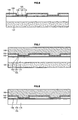
- Fig. 1 is a side-sectional view of a semiconductor light emitting device according to a first embodiment.
- Fig. 2A is a plan view of Fig. 1 .
- Fig. 3 is a circuit diagram illustrating an equivalent circuit of Fig. 1 .
- Figs. 4 to 11 are diagrams illustrating a process of manufacturing the semiconductor light emitting device in Fig. 1 .
- Fig. 12 is a side-sectional view of a semiconductor light emitting device according to a second embodiment.
- Fig. 13 is a bottom view of Fig. 11 .
- Fig. 14 is a side-sectional view of a semiconductor light emitting device according to a third embodiment.
- Fig. 15 a bottom view of a semiconductor light emitting device according to a fourth embodiment.
- Fig. 1 is a side-sectional view of a semiconductor light emitting device according to a first embodiment
- Fig. 2 is a plan view of Fig. 1
- Fig. 3 is a circuit diagram illustrating an equivalent circuit of Fig. 1 .
- a semiconductor light emitting device 100 includes a light emitting structure 135, a first insulating layer 140, a second electrode layer 150, a conductive supporting member 160, a second insulating layer 180, and a metal layer 190.
- the light emitting structure 135 includes an LED using a plurality of compound semiconductor layers, for example, group III-V compound semiconductors, and the LED may be a colored LED or a UV LED which emits blue light, green light, or red light. Light emitted by the LED may be diversely implemented within the technical scope of embodiments.
- the compound semiconductor may have, but is not limited to, a formula of In x AlyGa 1-x-y N (where 0 ⁇ x ⁇ 1, 0 ⁇ y ⁇ 1, 0 ⁇ x+y ⁇ 1).
- the light emitting structure 135 includes a first conductive semiconductor layer 110, an active layer 120, and a second conductive semiconductor layer 130.
- the first conductive semiconductor layer 110 may be formed of at least one of the compound semiconductors of group III-V elements doped with a first conductive dopant, for example, GaN, AlN, AlGaN, InGaN, InN, InAlGaN, AlInN, AlGaAs, GaP, GaAs, GaAsP, and AlGaInP.
- a first conductive dopant for example, GaN, AlN, AlGaN, InGaN, InN, InAlGaN, AlInN, AlGaAs, GaP, GaAs, GaAsP, and AlGaInP.
- the first conductive dopant includes an N-type dopant such as si, Ge, Sn, Se, and Te.
- the first conductive semiconductor layer 110 may be formed in a mono- or multi-layer, but is not limited thereto.
- a first electrode 171 is formed under the first conductive semiconductor layer 110, and the first electrode 171 may be formed in a predetermined pattern with a predetermined shape, but is not limited thereto.
- the first electrode 171 may include a bonding pad.
- the first electrode 171 may be formed using a material selected from the group consisting of, but is not limited to, Ti, Al, In, Ta, Pd, Co, Ni, Si, Ge, Ag, and Au.
- the active layer 120 is formed on the first conductive semiconductor layer 110, and may be formed in a single quantum well structure or a multiple quantum well structure.
- the active layer 120 may be periodically formed by the structure of a well layer and a barrier layer, for example, an InGaN well layer/GaN barrier layer by using the compound semiconductor material of group III-V elements.
- a conductive clad layer may be formed on and/or under the active layer 120, and the conductive clad layer may be formed of an AlGaN-based semiconductor.
- the second conductive semiconductor layer 130 is formed on the active layer 120, and may be formed of at least one of the compound semiconductors of group III-V elements doped with a second conductive dopant, for example, GaN, AlN, AlGaN, InGaN, InN, InAlGaN, AlInN, AlGaAs, GaP, GaAs, GaAsP, and AlGaInP.
- a second conductive dopant for example, GaN, AlN, AlGaN, InGaN, InN, InAlGaN, AlInN, AlGaAs, GaP, GaAs, GaAsP, and AlGaInP.
- the second conductive dopant includes a P-type dopant such as Mg and Zn.
- the second conductive semiconductor layer 130 may be formed in a mono- or multi-layer, but is not limited thereto.
- the first conductive semiconductor layer 110, the active layer 120, and the second conductive semiconductor layer 130 may be defined as a light emitting structure 135.
- an N-type semiconductor layer or a P-type semiconductor layer may be also provided on the second conductive layer 120.
- the first conductive semiconductor layer 110 may include a P-type semiconductor layer
- the second conductive semiconductor layer 130 may include an N-type semiconductor layer.
- the light emitting structure 135 may include at least one selected from the group consisting of an N-P junction, a P-N junction, an N-P-N junction, and a P-N-P junction.
- the first insulating layer 140 is formed on the top circumference of the second conductive semiconductor layer 130.
- the first insulating layer 140 may be formed in a continuous pattern with a belt shape, a loop shape, and a frame shape on the circumference region of the second conductive semiconductor layer 130.
- the first insulating layer 140 may be formed of a transparent insulating material, which may include SiO 2 , SiO x , SiO x N y , or Si 3 N 4 .
- the first insulating layer 140 may improve adhesive force with a material for the second conductive semiconductor layer 130.
- the first insulating layer 140 may be formed with a width or thickness of 2 ⁇ m or less, but is not limited thereto.
- the outer side of the first insulating layer 140 is exposed to the outer circumference 105 of the first conductive semiconductor layer 110, the active layer 120, and the second conductive semiconductor layer 130. Accordingly, the first insulating layer 140 may separate the second electrode layer 150 from the second conductive semiconductor layer 130.
- a laser irradiated during the manufacturing process is transmitted through the first insulating layer 140 to solve the side delamination of the light emitting structure 135.
- the first insulating layer 140 may also prevent metal debris generated by the second electrode layer 150 or the conductive supporting member 160 from being introduced into the outer side of the semiconductor layer 110, 120, and 130.
- the first insulating layer 140 may inhibit moisture from being penetrated into the outer side of the semiconductor layer 110, 120, and 130.
- a second electrode layer may be formed on the first insulating layer 140 and the second conductive semiconductor layer 130.
- the second electrode layer may include the second electrode layer 150 and the conductive supporting member 160.
- the second electrode layer 150 is formed at the outer side of the top of the second conductive semiconductor layer 130, which may be comprised at least one of an ohmic contact layer, a reflective layer, a adhesive layer and a seed metal.
- the ohmic contact layer may be formed in the form of a layer or a plurality of patterns.
- the ohmic contact layer may be comprised at least one of a metal material and an oxide material.
- the ohmic contact layer may comprise at least one selected from the group consisting of ITO, IZO, IZTO, IAZO, IGZO, IGTO, AZO, ATO, GZO, IrOx, RuOx, RuOx/ITO, Ni/IrOx/Au, Ni/IrOx/Au/ITO, Pt, Ni, Au, Rh and Pd .
- the ohmic contact layer may have a thickness of about 10 ⁇ to about 1 ⁇ m . However, the embodiment is not limited thereto.
- the reflective layer may be formed at least one of layers and formed of at least one of Ag, Ni, Al, Rh, Pd, Ir, Ru, Mg, Zn, Pt, Au and Hf, and materials consisting of the selective combination of these elements.
- the adhesive layer may be formed at least one of layers and formed of at least one of Ti, Au, Sn, Ni, Cr, Ga, In, Bi, Cu, Ag, and Ta, and materials consisting of the selective combination of these elements.
- the second electrode layer 150 may be used as a seed layer for a plating process.
- the seed layer may be formed at least one of Ti, Cr, Ta, Cr/Au, Cr/Cu, Ti/Au, Ta/Cu, and Ta/Ti/Cu.
- the conductive supporting member 160 may be formed on the second electrode layer 150.
- the conductive supporting member 160 may function as a base substrate, and its material may include copper (Cu), gold (Au), nickel (Ni), molybdenum (Mo), copper-tungsten (Cu-W), and carrier wafer such as Si, Ge, GaAs, ZnO, and SiC, SiGe, and GaN.
- the conductive supporting member 160 may be formed by an electroplating technique or in the form of a sheet, but is not limited thereto.
- the conductive supporting member 160 may be formed with a thickness of about 30 ⁇ m to about 150 ⁇ m, but is not limited thereto.
- a second insulating layer 180 is formed at the outer side of the light emitting structure 135.
- the second insulating layer 180 is formed along the outer side of the first conductive semiconductor layer 110, the active layer 120, and the second conductive semiconductor layer 130, and one end 181 is disposed under some portions of the first electrode 171 and the other end is disposed under the first insulating layer 140.
- the metal layer 190 includes a connection pattern 191 and a loop pattern 193.
- the connection pattern 191 is formed under the second insulating layer 180, one end is electrically connected to the first electrode 171, and the other end is electrically connected to the loop pattern 193.
- the second insulating layer 180 is disposed between the connection pattern 191 of the metal layer 190 and the semiconductor layer 110, 120, and 130 to insulate them.
- the metal layer 190 may be formed in a mono- or multi-layer of at least one selected from the group consisting of Ti, Al, In, Ta, Pd, co, Ni, Si, Ge, Ag, Au, and an alloy thereof.
- the loop pattern 193 is electrically connected to the connection pattern 191 of the metal layer 190, and disposed along the bottom circumference of the first insulating layer 140. Accordingly, the loop pattern 193 of the metal layer 190 and the second electrode layer face each other on both sides of the first insulating layer 140.
- a first current path passing through the light emitting structure 135 and a second current path corresponding to the first insulating layer 140 may be disposed in parallel.
- the first insulating layer 140 functions as a capacitor 100B between the loop pattern 193 of the metal layer 190 and the second electrode layer 150, and the capacitor 100B is parallel connected to both ends P1 and P2 of the light emitting device 100A.
- the capacitor 100B may charge and discharge an ESD voltage applied to the light emitting structure 100 to protect the semiconductor layer 110, 120, and 130 of the light emitting structure 135. Accordingly, a device having characteristic which is robust against ESD may be provided by including a built-in capacitor 100B.
- the capacitance of the capacitor 100B may be controlled to line width or thickness of the metal layer 190, and then may be controlled in consideration of electrical characteristics of the light emitting structure 135.
- Figs. 4 to 11 are diagrams illustrating a process of manufacturing the semiconductor light emitting device in Fig. 1
- a substrate 100 is loaded into growth equipment, and a compound semiconductor layer of group II to group VI elements is formed thereon.
- the growth equipment may include an electron beam evaporator, physical vapor deposition (PVD), chemical vapor deposition (CVD), plasma laser deposition (PLD), dual-type thermal evaporator, sputtering and metal organic chemical vapor deposition (MOCVD), but is not limited thereto.
- PVD physical vapor deposition
- CVD chemical vapor deposition
- PLD plasma laser deposition
- MOCVD metal organic chemical vapor deposition
- the substrate 101 may be selected from the group consisting of sapphire substrate (Al 2 O 3 ), GaN, SiC, ZnO, Si, GaP, InP, Ga 2 O 3 , conductive substrate, and GaAs.
- a concave-convex pattern may be formed on the top of the substrate 101.
- a layer or pattern using a compound semiconductor of group II to group VI elements, for example, at least one selected from the group consisting of ZnO layer (not shown), buffer layer (not shown), and undoped semiconductor layer (not shown) may be formed.
- the buffer layer and the undoped semiconductor layer may be formed using a compound semiconductor of group III-V elements, the buffer layer may decrease a lattice constant difference with the substrate, and the undoped semiconductor layer may be formed of an undoped GaN-based semiconductor.
- a light emitting structure 135 including a plurality of compound semiconductor layers may be formed on the substrate 101.
- the light emitting structure 135 includes a first conductive semiconductor layer 110, an active layer 120, and a second conductive semiconductor layer 130.
- the first conductive semiconductor layer 110 is formed on the substrate 101 or another semiconductor layer
- the active layer 120 is formed on the first conductive semiconductor layer 110
- the second conductive semiconductor layer 130 is formed on the active layer 120.
- the first conductive semiconductor layer 110 may be formed of at least one of the compound semiconductors of group III-V elements doped with a first conductive dopant, for example, GaN, AlN, AlGaN, InGaN, InN, InAlGaN, AlInN, AlGaAs, GaP, GaAs, GaAsP, and AlGaInP.
- a first conductive dopant for example, GaN, AlN, AlGaN, InGaN, InN, InAlGaN, AlInN, AlGaAs, GaP, GaAs, GaAsP, and AlGaInP.
- the first conductive dopant includes an N-type dopant such as si, Ge, Sn, Se, and Te.
- the first conductive semiconductor layer 110 may be formed in a mono- or multi-layer, but is not limited thereto.
- An active layer 120 is formed on the first conductive semiconductor layer 110, and the active layer 120 may be formed in a single quantum well structure or a multiple quantum well structure.
- the active layer 120 may be periodically formed by a well layer and a barrier layer, for example, an InGaN well layer/GaN barrier layer by using the compound semiconductor material of group III-V elements.
- a conductive clad layer may be formed on and/or under the active layer 120, and the conductive clad layer may be formed of an AlGaN-based semiconductor.
- the second conductive semiconductor layer 130 is formed on the active layer 120, and the second conductive semiconductor layer 130 may be formed of at least one of the compound semiconductors of group III-V elements doped with a second conductive dopant, for example, GaN, AlN, AlGaN, InGaN, InN, InAlGaN, AlInN, AlGaAs, GaP, GaAs, GaAsP, and AlGaInP.
- the second conductive dopant includes a P-type dopant such as Mg and Zn.
- the second conductive semiconductor layer 130 may be formed in a mono- or multi-layer, but is not limited thereto.
- a third conductive semiconductor layer for example, an N-type semiconductor layer or a P-type semiconductor layer may be formed on the second conductive semiconductor layer 130. Accordingly, at least one selected from the group consisting of an N-P junction, a P-N junction, an N-P-N junction, and a P-N-P junction structure may be formed in the light emitting structure 135.
- a mask pattern is used on a chip boundary region on the second conductive semiconductor layer 130 to form a first insulating layer 140.
- the first insulating layer 140 is formed along the outer circumference of the top of the second conductive semiconductor layer 130 of an individual chip, and the shape may be formed in a continuous pattern with a belt shape, a loop shape, and a frame shape (eg: closed loop shape). In this case, the inner region of the second conductive semiconductor layer 130 is exposed.
- the first insulating layer 140 may be formed of at least one selected from transparent insulating materials with a predetermined dielectric constant, for example, the group consisting of SiO 2 , SiO x , SiO x N y , and Si 3 N 4 , but is not limited thereto.
- the first insulating layer 140 is formed of a material which is transmitted by laser light and has little debris generated by laser light and may improve adhesive force with the second conductive semiconductor layer 130.
- the first insulating layer 140 may be formed with a width or thickness of 2 ⁇ m or less, but is not limited thereto.
- a second electrode layer 150 is formed on the second conductive semiconductor layer 130 and the first insulating layer 140.
- the second electrode layer 150 may comprise at least one of an ohmic contact layer, a reflective layer, and an adhesive layer.
- the ohmic contact layer may be formed in the form of a layer or a plurality of patterns.
- the ohmic contact layer may be comprised at least one of a metal material and an oxide material.
- the ohmic contact layer may comprise at least one selected from the group consisting of ITO, IZO, IZTO, IAZO, IGZO, IGTO, AZO, ATO, GZO, IrOx, RuOx, RuOx/ITO, Ni/IrOx/Au, Ni/IrOx/Au/ITO, Pt, Ni, Au, Rh and Pd .
- the ohmic contact layer may have a thickness of about 10 ⁇ to about 1 ⁇ m. However, the embodiment is not limited thereto.
- the reflective layer may be formed at least one of layers and formed of at least one of Ag, Ni, Al, Rh, Pd, Ir, Ru, Mg, Zn, Pt, Au and Hf, and materials consisting of the selective combination of these elements.
- the adhesive layer may be formed at least one of layers and formed of at least one of Ti, Au, Sn, Ni, Cr, Ga, In, Bi, Cu, Ag, and Ta, and materials consisting of the selective combination of these elements.
- the second electrode layer 150 may be used as a seed layer for a plating process.
- the seed layer may be formed at least one of Ti, Cr, Ta, Cr/Au, Cr/Cu, Ti/Au, Ta/Cu, and Ta/Ti/Cu.
- a conductive supporting member 160 may be formed on the second conductive layer 150, the conductive supporting member 160 may function as a base substrate, and its material may include copper (Cu), gold (Au), nickel (Ni), molybdenum (Mo), copper-tungsten (Cu-W), and carrier wafer such as Si, Ge, GaAs, ZnO, and SiC, SiGe, and GaN.
- the conductive supporting member 160 may be formed by an electroplating technique or in the form of a sheet, but is not limited thereto.
- the conductive supporting member 160 may be formed with a thickness of about 30 ⁇ m to about 150 ⁇ m, but is not limited thereto.
- the conductive supporting member 160 is disposed on the base to remove the substrate 101.
- the substrate 101 is removed through a physical and/or chemical method.
- the physical removal method separates the substrate 101 by irradiating a laser of a predetermined wavelength on the substrate 101 (Laser Lift Off: LLO).
- the substrate 101 may be separated by removing the buffer layer through a chemical removal method using a wet etchant.
- the substrate removal method is not limited to the chemical removal method.
- a polishing process may be performed by an inductively coupled plasma/reactive ion etching (ICP/RIE) method on the surface of the first conductive semiconductor layer 110 with the substrate 101 removed.
- ICP/RIE inductively coupled plasma/reactive ion etching
- isolation etching is performed on the chip-to-chip boundary region (ie, channel region) to separate the region into chip units. Then, the outer circumference 105 of the light emitting structure 135 is etched to expose the first insulating layer 140. In this case, outer side of the first insulating layer 140 is exposed to the outer circumference 105 of the light emitting structure 135, and the outer circumference of the first insulating layer 140 may separate the second electrode layer 150 from the side wall of the light emitting structure 135.
- the light emitting structure 135 has an effect of being inwardly shifted from the outer wall of the chip.
- a first electrode 171 is formed under the first conductive semiconductor layer 110.
- the first electrode 171 may be formed in a predetermined shape and a predetermined pattern, but is not limited thereto.
- a process of forming the first electrode 171 may be performed before or after the isolation etching or after the chip separation, but is not limited thereto.
- a second insulating layer 180 is formed on a predetermined region of the light emitting structure 135 using a mask pattern.
- the second insulating layer 180 is formed with a predetermined width extending from the first electrode 171 to the position of the first insulating layer 140 to cover the bottom of the first conductive semiconductor layer 110 and some portions of the side wall of the semiconductor layer 110, 120, and 130.
- an end 181 of the second insulating layer 180 may be extended into the bottom of the first electrode 171.
- the second insulating layer 180 may be formed of one selected from the group consisting of SiO 2 , SiO x , SiO x N y , and Si 3 N 4 , or formed of a material identical to the first insulating layer 140 or another material.
- a metal layer 190 is formed under the second insulating layer 180 and the first insulating layer 140, and the metal layer 190 includes a connection pattern 191 and a loop pattern 193.
- the connection pattern 191 of the metal layer 190 is formed under (ie, at the outer side of) the second insulating layer 180, and is electrically connected to the first electrode 171.
- the loop pattern 193 of the metal layer 190 is connected to the other end of the connection pattern 191, is disposed along the bottom circumference of the first insulating layer 140, and is separated from the outer wall of the light emitting structure 135.
- the loop pattern 193 may be formed in an open loop shape or a closed loop shape along the bottom circumference of the first insulating layer 140.
- the metal layer 190 may be formed in a mono- or multi-layer of at least one selected from the group consisting of Ti, In, Ta, Pd, Co, Ni, Si, Ge, Ag, Au, and an alloy thereof.
- connection pattern 191 of the metal layer 190 is electrically connected to the first electric 171, and the loop pattern 193 is disposed to correspond to the second electrode 150.
- the loop pattern 193 of the metal layer 190 may be formed in a pattern shape with a predetermined width under the first insulating layer 140, that is, may be formed in a structure as in Fig. 2 . Then, the first insulating layer 140 is disposed between the loop pattern 193 of the metal layer 190 and the second electrode 150 to function as a capacitor.
- the capacitor is formed in a parallel structure with respect to the light emitting structure 135 to be charged or discharged by an abnormal power source (eg: ESD) applied to the light emitting structure 135. Accordingly, the light emitting structure 135 may be protected from the abnormal power source.
- ESD abnormal power source
- the semiconductor light emitting device is separated into chip units based on the boundary of the chips. Then, laser may be used for a chip separation method.
- the chip may provide a vertical semiconductor light emitting device with a capacitor.
- Fig. 12 is a side-sectional view of a semiconductor light emitting device according to a second embodiment
- Fig. 13 is a bottom view of Fig. 11 .
- description of the second embodiment a repeated description about the portion identical to the first embodiment will be omitted with reference to the first embodiment.
- a semiconductor light emitting device 100A includes a light emitting structure 135, a insulating layer 140A with an protrusion 145, a second electrode layer 150, a conductive supporting member 160, and a metal layer 190.
- the insulating layer 140A may be formed in a continuous pattern (eg: closed loop shape) with a belt shape, a loop shape, and a frame shape on the bottom circumference of the second conductive semiconductor layer 130.
- the insulating layer 140A may include at least one selected from translucent insulating layers, for example, the group consisting of SiO 2 , SiO x , SiO x N y , Si 3 N 4 , Al 2 O 3 , and TiO 2 by using a mask pattern.
- a second conductive layer 150 and the conductive supporting member 160 are formed on the insulating layer 140A and the second conductive semiconductor layer 130.
- a protrusion 145 is formed under the inner side of the insulating layer 140.
- the protrusion 145 may be formed with a depth at which the first conductive semiconductor layer 110 is exposed.
- the protrusion 145 of the insulating layer 140 may be formed in a continuously closed loop shape such as a belt shape or a loop shape, may be formed within a distance of about 1 ⁇ m to about 5 ⁇ m (D1) from the outer wall of the semiconductor layer 110, 120, and 130, and the distance range may be varied according to the size of the chip.
- the cross-sectional shape of the protrusion 145 may be formed in a domed shape, a semi-elliptical shape, a horn shape, a truncated-horn shape, and a polygon shape and the shape may be modified.
- the protrusion 145 of the insulating layer 140A may separate the light emitting structure 135 into an inner active region A1 and an outer inactive region A2.
- the semiconductor layer 110, 120, and 130 in the active region A1 is normally operated, and the semiconductor layer in the inactive region A2 is not normally operated.
- a first conductive semiconductor layer 110 in the inactive region A2 may be used partially in current path.
- a second insulating layer 180 in Fig. 1 may not be formed under the connection pattern 191 of the metal layer 190. Accordingly, a process of forming the second insulating layer may be removed.
- connection pattern 191 of the metal layer 190 and the semiconductor layer 110, 120, and 130 of the light emitting structure 135 may be solved by the protrusion 145 of the insulating layer 140A.
- the loop pattern 193 of the metal layer 190 may not be separated from the outer side of the light emitting structure 135.
- the active region is normally operated because the protrusion 145 of the insulating layer 140A inactivates the outer side of the light emitting structure 135.
- the protrusion 145 of the active layer 140A may prevent moisture from being penetrated into the outer side of the chip. Because the protrusion 145 of the insulating layer 140 may be formed in a single or a double concave-convex structure, it may reinforce adhesive force with the light emitting structure 135.
- Fig. 14 is a side-sectional view of a semiconductor light emitting device according to a third embodiment.
- a repeated description about the portion identical to the second embodiment will be omitted with reference to the second embodiment.
- a semiconductor light emitting device 100B includes a light emitting structure 135, a insulating layer 140A with an protrusion 145A, a second electrode layer 150, a conductive supporting member 160, and a metal layer 190.
- the insulating layer 140A may be formed in a continuous pattern (eg: closed loop shape) with a belt shape, a loop shape, and a frame shape on the bottom circumference of the second conductive semiconductor layer 130.
- the insulating layer 140A may include at least one selected from translucent insulating layers, for example, the group consisting of SiO 2 , SiO x , SiO x N y , Si 3 N 4 , Al 2 O 3 , and TiO 2 by using a mask pattern.
- a second conductive layer 150 and the conductive supporting member 160 are formed on the insulating layer 140A and the second conductive semiconductor layer 130.
- a protrusion 145A is formed under the inner side of the insulating layer 140.
- the protrusion 145A may be formed with a depth at which the first conductive semiconductor layer 110 is exposed.
- the protrusion 145A of the insulating layer 140 may be formed in a continuously closed loop shape such as a belt shape or a loop shape, may be formed to the outer wall of the semiconductor layer 110, 120, and 130.
- the cross-sectional shape of the protrusion 145A may be formed in a polygon shape, a semi-elliptical shape, a horn shape, a truncated-horn shape, and a domed shape and the shape may be modified.
- An outer wall of the light emitting structure 135 is electrically opened by the protrusion 145A of the insulating layer 140A. Accordingly, the second insulating layer is not formed on the light emitting structure 135.
- the protrusion 145A of the insulating layer 140A may be formed on the circumference of the region, on which a loop pattern 193 of the metal layer 190 is disposed, to inactivate the region.
- the area of the active layer 120 may be increased with respect to the active layer of the second embodiment.
- Fig. 15 a bottom view of a semiconductor light emitting device according to a fourth embodiment.
- a repeated description about the portion identical to the embodiments will be omitted with reference to the embodiments.
- a semiconductor light emitting device an insulating layer 140 with a protrusion 145B, a second electrode layer 150, a conductive supporting member 160, and a metal layer 190.
- the insulating layer 140 may be formed in a continuous pattern (eg: closed loop shape) with a belt shape, a loop shape, and a frame shape on the bottom circumference of the second conductive semiconductor layer 130.
- a protrusion 145B is formed under the inner side of the insulating layer 140.
- the protrusion 145B of the insulating layer may be formed with a depth at which the first conductive semiconductor layer 110 is exposed and contacted to the first conductive semiconductor 110.
- the protrusion 145A of the insulating layer 140 may be formed in a continuously closed loop shape such as a belt shape or a loop shape, may be formed to a portion area of the semiconductor layer 110, 120, and 130.
- the opened portion area of the light emitting structure 135 is electrically opened by the protrusion 145B of the insulating layer 140. Accordingly, the second insulating layer is not formed on the light emitting structure 135.
- the protrusion 145B of the insulating layer 140 may be formed on the circumference of the opened portion area, on which a connection pattern 191 of the metal layer 190 is disposed, to inactive region A1. In this case, the area of the active layer 120 may be increased.
- the metal layer 190 includes a connection pattern 191 and a loop pattern 193.
- the connection pattern 191 is electrically connected to the first electrode 171, and the other end is electrically connected to the loop pattern 193.
- the connection pattern 191 is disposed to the opened portion area or the inactive region A1.
- the loop pattern 193 is electrically connected to the connection pattern 191 of the metal layer 190, and disposed along the bottom circumference of the first insulating layer 140. Accordingly, the loop pattern 193 of the metal layer 190 and the second electrode layer face each other on both sides of the first insulating layer 140.
- a first current path passing through the light emitting structure 135 and a second current path corresponding to the first insulating layer 140 may be disposed in parallel.
- a method for manufacturing a semiconductor light emitting device comprising: forming a plurality of compound semiconductor layers to form a light emitting structure; forming a first insulating layer on the top circumference of the light emitting structure; forming a second electrode layer on the first insulating layer and the light emitting structure; forming a first electrode under the light emitting structure; and forming a metal layer comprising a loop pattern on the bottom circumference of the first insulating layer and a connection pattern connected to the first electrode.
- first and second embodiments were centered on each embodiment, the description may be performed by applying the first embodiment in combination with the second embodiment, and the second embodiment in combination with the first embodiment, but is not limited to characteristics of each embodiment.
- Embodiments can provide a vertical semiconductor light emitting device including a built-in capacitor.
- Embodiments can provide a vertical semiconductor light emitting device robust against ESD.
- Embodiments can provide a light emitting device robust against moisture by opening the outer side of the light emitting structure.
- Embodiments can improve adhesive force between a semiconductor layer and another layer.
- Embodiments can prevent interlayer short defects of a plurality of compound semiconductor layers.
- Embodiments can improve the reliability of the vertical semiconductor light emitting device.
- Embodiments can provide a semiconductor light emitting device like LED.
- Embodiments can improve the electrical reliability of the semiconductor light emitting device.
- Embodiments can improve the light efficiency of the vertical semiconductor light emitting device.
- Embodiments can apply a light source including a packaged semiconductor light emitting device to an illumination field, an indication field, and a display field.
Abstract

Description
- The present application claims priority under 35 U.S.C. 119 and 35 U.S.C. 365 to Korean Patent Application No.
10-2008-0105257 (filed on October 27, 2008 - The present disclosure relates to a semiconductor light emitting device.
- Group III-V nitride semiconductors have been in the spotlight as a core material for light emitting devices, such as light emitting diodes (LEDs), laser diodes (LDs), and the like, due to excellent physical and chemical properties thereof. The III-V nitride semiconductor includes a semiconductor material having the formula InxAlyGa1-x-yN (where 0≦x≦1, 0≦y≦1, 0≦x+y≦1).
- A Light Emitting Diode (LED) is a kind of semiconductor device that converts electricity into infrared rays or light using the characteristics of a compound semiconductor to transmit and receive a signal, or is used as a light source.
- The LEDs or Laser diodes (LDs) made of these nitride semiconductor materials are extensively adopted in light emitting devices for obtaining light, and are applied as a light source for various products such as a keypad light emitting diode of a mobile phone, an electrical sign board, and a lighting device.
- Embodiments provide a semiconductor light emitting device with a capacitor structure.
- Embodiments provide a semiconductor light emitting device to improve ESD (electro-static discharge) characteristics by disposing an insulating layer between a metal layer and a second electrode layer to embody a capacitor.
- An embodiment provides a semiconductor light emitting device comprising: a light emitting structure comprising a plurality of compound semiconductor layers; a first electrode under the light emitting structure; a second electrode layer on the light emitting structure; a first insulating layer between the light emitting structure and the second electrode layer; and a metal layer formed under the first insulating layer and electrically connected to the first electrode.
- An embodiment provides a semiconductor light emitting device comprising: a light emitting structure comprising a first conductive semiconductor layer, an active layer on the first conductive semiconductor layer, and a second conductive semiconductor layer on the active layer; a first electrode under the first conductive semiconductor layer; a second electrode layer on the second conductive semiconductor layer; a second insulating layer on an outer side of the light emitting structure; a first insulating layer under the second electrode layer; and a metal layer comprising a loop pattern under a circumference of the first insulating layer and a connection pattern electrically connected to the first electrode on the second insulating layer.
- An embodiment provides a semiconductor light emitting device comprising: a first conductive semiconductor layer; an active layer on the first conductive semiconductor layer; a second conductive semiconductor layer on the active layer; a first electrode under the first conductive semiconductor layer; a second electrode layer on the second conductive semiconductor layer; a first insulating layer between the second conductive semiconductor layer and the second electrode layer; and a metal layer formed under the first insulating layer and electrically connected to the first electrode, wherein the first insulating layer comprises a protrusion disposed in a closed loop shape on a certain regions from the second conductive semiconductor layer to the upper portion of the first conductive semiconductor layer.
- The details of one or more embodiments are set forth in the accompanying drawings and the description below. Other features will be apparent from the description and drawings, and from the claims.
-
Fig. 1 is a side-sectional view of a semiconductor light emitting device according to a first embodiment. -
Fig. 2A is a plan view ofFig. 1 . -
Fig. 3 is a circuit diagram illustrating an equivalent circuit ofFig. 1 . -
Figs. 4 to 11 are diagrams illustrating a process of manufacturing the semiconductor light emitting device inFig. 1 . -
Fig. 12 is a side-sectional view of a semiconductor light emitting device according to a second embodiment. -
Fig. 13 is a bottom view ofFig. 11 . -
Fig. 14 is a side-sectional view of a semiconductor light emitting device according to a third embodiment. -
Fig. 15 a bottom view of a semiconductor light emitting device according to a fourth embodiment. - Reference will now be made in detail to the embodiments of the present disclosure, examples of which are illustrated in the accompanying drawings. In description of embodiments, the 'on' or 'under' of each layer may be described with reference to the accompanying drawings, and the thickness of the each layer will also be described as an example and is not limited to the thickness of the accompanying drawings.
- In description of embodiments, it will be understood that in a case where a layer (or film), a region, a pattern, or components is referred to as being 'on' or 'under' another substrate, layer (or film), region or patterns, the 'on' and 'under' include all the meanings of 'directly' and 'indirectly'.
-
Fig. 1 is a side-sectional view of a semiconductor light emitting device according to a first embodiment,Fig. 2 is a plan view ofFig. 1 , andFig. 3 is a circuit diagram illustrating an equivalent circuit ofFig. 1 . - Referring to
Figs. 1 and 2 , a semiconductorlight emitting device 100 includes alight emitting structure 135, a firstinsulating layer 140, asecond electrode layer 150, a conductive supportingmember 160, a secondinsulating layer 180, and ametal layer 190. - The
light emitting structure 135 includes an LED using a plurality of compound semiconductor layers, for example, group III-V compound semiconductors, and the LED may be a colored LED or a UV LED which emits blue light, green light, or red light. Light emitted by the LED may be diversely implemented within the technical scope of embodiments. The compound semiconductor may have, but is not limited to, a formula of InxAlyGa1-x-yN (where 0≦x≦1, 0≦y≦1, 0≦x+y≦1). - The
light emitting structure 135 includes a firstconductive semiconductor layer 110, anactive layer 120, and a secondconductive semiconductor layer 130. - The first
conductive semiconductor layer 110 may be formed of at least one of the compound semiconductors of group III-V elements doped with a first conductive dopant, for example, GaN, AlN, AlGaN, InGaN, InN, InAlGaN, AlInN, AlGaAs, GaP, GaAs, GaAsP, and AlGaInP. In a case where the firstconductive semiconductor layer 110 is an N-type semiconductor, the first conductive dopant includes an N-type dopant such as si, Ge, Sn, Se, and Te. The firstconductive semiconductor layer 110 may be formed in a mono- or multi-layer, but is not limited thereto. - A
first electrode 171 is formed under the firstconductive semiconductor layer 110, and thefirst electrode 171 may be formed in a predetermined pattern with a predetermined shape, but is not limited thereto. Thefirst electrode 171 may include a bonding pad. - The
first electrode 171 may be formed using a material selected from the group consisting of, but is not limited to, Ti, Al, In, Ta, Pd, Co, Ni, Si, Ge, Ag, and Au. - The
active layer 120 is formed on the firstconductive semiconductor layer 110, and may be formed in a single quantum well structure or a multiple quantum well structure. Theactive layer 120 may be periodically formed by the structure of a well layer and a barrier layer, for example, an InGaN well layer/GaN barrier layer by using the compound semiconductor material of group III-V elements. A conductive clad layer may be formed on and/or under theactive layer 120, and the conductive clad layer may be formed of an AlGaN-based semiconductor. - The second
conductive semiconductor layer 130 is formed on theactive layer 120, and may be formed of at least one of the compound semiconductors of group III-V elements doped with a second conductive dopant, for example, GaN, AlN, AlGaN, InGaN, InN, InAlGaN, AlInN, AlGaAs, GaP, GaAs, GaAsP, and AlGaInP. In a case where the secondconductive semiconductor layer 130 is a P-type semiconductor, the second conductive dopant includes a P-type dopant such as Mg and Zn. The secondconductive semiconductor layer 130 may be formed in a mono- or multi-layer, but is not limited thereto. - The first
conductive semiconductor layer 110, theactive layer 120, and the secondconductive semiconductor layer 130 may be defined as alight emitting structure 135. - An N-type semiconductor layer or a P-type semiconductor layer may be also provided on the second
conductive layer 120. In addition, the firstconductive semiconductor layer 110 may include a P-type semiconductor layer, while the secondconductive semiconductor layer 130 may include an N-type semiconductor layer. Accordingly, thelight emitting structure 135 may include at least one selected from the group consisting of an N-P junction, a P-N junction, an N-P-N junction, and a P-N-P junction. - The first
insulating layer 140 is formed on the top circumference of the secondconductive semiconductor layer 130. The firstinsulating layer 140 may be formed in a continuous pattern with a belt shape, a loop shape, and a frame shape on the circumference region of the secondconductive semiconductor layer 130. - The first
insulating layer 140 may be formed of a transparent insulating material, which may include SiO2, SiOx, SiOxNy, or Si3N4. - The first
insulating layer 140 may improve adhesive force with a material for the secondconductive semiconductor layer 130. The first insulatinglayer 140 may be formed with a width or thickness of 2 µm or less, but is not limited thereto. - The outer side of the first
insulating layer 140 is exposed to theouter circumference 105 of the firstconductive semiconductor layer 110, theactive layer 120, and the secondconductive semiconductor layer 130. Accordingly, the firstinsulating layer 140 may separate thesecond electrode layer 150 from the secondconductive semiconductor layer 130. - A laser irradiated during the manufacturing process is transmitted through the first
insulating layer 140 to solve the side delamination of thelight emitting structure 135. The firstinsulating layer 140 may also prevent metal debris generated by thesecond electrode layer 150 or the conductive supportingmember 160 from being introduced into the outer side of thesemiconductor layer insulating layer 140 may inhibit moisture from being penetrated into the outer side of thesemiconductor layer - A second electrode layer may be formed on the first
insulating layer 140 and the secondconductive semiconductor layer 130. The second electrode layer may include thesecond electrode layer 150 and the conductive supportingmember 160. - The
second electrode layer 150 is formed at the outer side of the top of the secondconductive semiconductor layer 130, which may be comprised at least one of an ohmic contact layer, a reflective layer, a adhesive layer and a seed metal. - The ohmic contact layer may be formed in the form of a layer or a plurality of patterns. The ohmic contact layer may be comprised at least one of a metal material and an oxide material. The ohmic contact layer may comprise at least one selected from the group consisting of ITO, IZO, IZTO, IAZO, IGZO, IGTO, AZO, ATO, GZO, IrOx, RuOx, RuOx/ITO, Ni/IrOx/Au, Ni/IrOx/Au/ITO, Pt, Ni, Au, Rh and Pd . The ohmic contact layer may have a thickness of about 10Å to about 1µm. However, the embodiment is not limited thereto. The reflective layer may be formed at least one of layers and formed of at least one of Ag, Ni, Al, Rh, Pd, Ir, Ru, Mg, Zn, Pt, Au and Hf, and materials consisting of the selective combination of these elements. The adhesive layer ma be formed at least one of layers and formed of at least one of Ti, Au, Sn, Ni, Cr, Ga, In, Bi, Cu, Ag, and Ta, and materials consisting of the selective combination of these elements. The
second electrode layer 150 may be used as a seed layer for a plating process. The seed layer may be formed at least one of Ti, Cr, Ta, Cr/Au, Cr/Cu, Ti/Au, Ta/Cu, and Ta/Ti/Cu. - The conductive supporting
member 160 may be formed on thesecond electrode layer 150. The conductive supportingmember 160 may function as a base substrate, and its material may include copper (Cu), gold (Au), nickel (Ni), molybdenum (Mo), copper-tungsten (Cu-W), and carrier wafer such as Si, Ge, GaAs, ZnO, and SiC, SiGe, and GaN. The conductive supportingmember 160 may be formed by an electroplating technique or in the form of a sheet, but is not limited thereto. The conductive supportingmember 160 may be formed with a thickness of about 30 µm to about 150 µm, but is not limited thereto. - A second insulating
layer 180 is formed at the outer side of thelight emitting structure 135. The secondinsulating layer 180 is formed along the outer side of the firstconductive semiconductor layer 110, theactive layer 120, and the secondconductive semiconductor layer 130, and oneend 181 is disposed under some portions of thefirst electrode 171 and the other end is disposed under the first insulatinglayer 140. - Referring to
Figs. 1 and 2 , themetal layer 190 includes aconnection pattern 191 and aloop pattern 193. Theconnection pattern 191 is formed under the second insulatinglayer 180, one end is electrically connected to thefirst electrode 171, and the other end is electrically connected to theloop pattern 193. - The second
insulating layer 180 is disposed between theconnection pattern 191 of themetal layer 190 and thesemiconductor layer - The
metal layer 190 may be formed in a mono- or multi-layer of at least one selected from the group consisting of Ti, Al, In, Ta, Pd, co, Ni, Si, Ge, Ag, Au, and an alloy thereof. - The
loop pattern 193 is electrically connected to theconnection pattern 191 of themetal layer 190, and disposed along the bottom circumference of the first insulatinglayer 140. Accordingly, theloop pattern 193 of themetal layer 190 and the second electrode layer face each other on both sides of the first insulatinglayer 140. - A first current path passing through the
light emitting structure 135 and a second current path corresponding to the first insulatinglayer 140 may be disposed in parallel. - Referring to
Fig. 3 , the first insulatinglayer 140 functions as acapacitor 100B between theloop pattern 193 of themetal layer 190 and thesecond electrode layer 150, and thecapacitor 100B is parallel connected to both ends P1 and P2 of thelight emitting device 100A. - The
capacitor 100B may charge and discharge an ESD voltage applied to thelight emitting structure 100 to protect thesemiconductor layer light emitting structure 135. Accordingly, a device having characteristic which is robust against ESD may be provided by including a built-incapacitor 100B. - The capacitance of the
capacitor 100B may be controlled to line width or thickness of themetal layer 190, and then may be controlled in consideration of electrical characteristics of thelight emitting structure 135. -
Figs. 4 to 11 are diagrams illustrating a process of manufacturing the semiconductor light emitting device inFig. 1 - Referring to
Fig. 4 , asubstrate 100 is loaded into growth equipment, and a compound semiconductor layer of group II to group VI elements is formed thereon. - The growth equipment may include an electron beam evaporator, physical vapor deposition (PVD), chemical vapor deposition (CVD), plasma laser deposition (PLD), dual-type thermal evaporator, sputtering and metal organic chemical vapor deposition (MOCVD), but is not limited thereto.
- The
substrate 101 may be selected from the group consisting of sapphire substrate (Al2O3), GaN, SiC, ZnO, Si, GaP, InP, Ga2O3, conductive substrate, and GaAs. A concave-convex pattern may be formed on the top of thesubstrate 101. A layer or pattern using a compound semiconductor of group II to group VI elements, for example, at least one selected from the group consisting of ZnO layer (not shown), buffer layer (not shown), and undoped semiconductor layer (not shown) may be formed. - The buffer layer and the undoped semiconductor layer may be formed using a compound semiconductor of group III-V elements, the buffer layer may decrease a lattice constant difference with the substrate, and the undoped semiconductor layer may be formed of an undoped GaN-based semiconductor.
- A
light emitting structure 135 including a plurality of compound semiconductor layers may be formed on thesubstrate 101. Thelight emitting structure 135 includes a firstconductive semiconductor layer 110, anactive layer 120, and a secondconductive semiconductor layer 130. The firstconductive semiconductor layer 110 is formed on thesubstrate 101 or another semiconductor layer, theactive layer 120 is formed on the firstconductive semiconductor layer 110, and the secondconductive semiconductor layer 130 is formed on theactive layer 120. - The first
conductive semiconductor layer 110 may be formed of at least one of the compound semiconductors of group III-V elements doped with a first conductive dopant, for example, GaN, AlN, AlGaN, InGaN, InN, InAlGaN, AlInN, AlGaAs, GaP, GaAs, GaAsP, and AlGaInP. In a case where the firstconductive semiconductor layer 110 is an N-type semiconductor, the first conductive dopant includes an N-type dopant such as si, Ge, Sn, Se, and Te. The firstconductive semiconductor layer 110 may be formed in a mono- or multi-layer, but is not limited thereto. - An
active layer 120 is formed on the firstconductive semiconductor layer 110, and theactive layer 120 may be formed in a single quantum well structure or a multiple quantum well structure. Theactive layer 120 may be periodically formed by a well layer and a barrier layer, for example, an InGaN well layer/GaN barrier layer by using the compound semiconductor material of group III-V elements. - A conductive clad layer may be formed on and/or under the
active layer 120, and the conductive clad layer may be formed of an AlGaN-based semiconductor. - The second
conductive semiconductor layer 130 is formed on theactive layer 120, and the secondconductive semiconductor layer 130 may be formed of at least one of the compound semiconductors of group III-V elements doped with a second conductive dopant, for example, GaN, AlN, AlGaN, InGaN, InN, InAlGaN, AlInN, AlGaAs, GaP, GaAs, GaAsP, and AlGaInP. In a case where the secondconductive semiconductor layer 130 is a P-type semiconductor, the second conductive dopant includes a P-type dopant such as Mg and Zn. The secondconductive semiconductor layer 130 may be formed in a mono- or multi-layer, but is not limited thereto. - In addition, a third conductive semiconductor layer, for example, an N-type semiconductor layer or a P-type semiconductor layer may be formed on the second
conductive semiconductor layer 130. Accordingly, at least one selected from the group consisting of an N-P junction, a P-N junction, an N-P-N junction, and a P-N-P junction structure may be formed in thelight emitting structure 135. - Referring to
Fig. 5 , a mask pattern is used on a chip boundary region on the secondconductive semiconductor layer 130 to form a first insulatinglayer 140. The first insulatinglayer 140 is formed along the outer circumference of the top of the secondconductive semiconductor layer 130 of an individual chip, and the shape may be formed in a continuous pattern with a belt shape, a loop shape, and a frame shape (eg: closed loop shape). In this case, the inner region of the secondconductive semiconductor layer 130 is exposed. - The first insulating
layer 140 may be formed of at least one selected from transparent insulating materials with a predetermined dielectric constant, for example, the group consisting of SiO2, SiOx, SiOxNy, and Si3N4, but is not limited thereto. - The first insulating
layer 140 is formed of a material which is transmitted by laser light and has little debris generated by laser light and may improve adhesive force with the secondconductive semiconductor layer 130. The first insulatinglayer 140 may be formed with a width or thickness of 2 µm or less, but is not limited thereto. - Referring to
Fig. 6 , asecond electrode layer 150 is formed on the secondconductive semiconductor layer 130 and the first insulatinglayer 140. Thesecond electrode layer 150 may comprise at least one of an ohmic contact layer, a reflective layer, and an adhesive layer. The ohmic contact layer may be formed in the form of a layer or a plurality of patterns. The ohmic contact layer may be comprised at least one of a metal material and an oxide material. The ohmic contact layer may comprise at least one selected from the group consisting of ITO, IZO, IZTO, IAZO, IGZO, IGTO, AZO, ATO, GZO, IrOx, RuOx, RuOx/ITO, Ni/IrOx/Au, Ni/IrOx/Au/ITO, Pt, Ni, Au, Rh and Pd . The ohmic contact layer may have a thickness of about 10Å to about 1µm. However, the embodiment is not limited thereto. The reflective layer may be formed at least one of layers and formed of at least one of Ag, Ni, Al, Rh, Pd, Ir, Ru, Mg, Zn, Pt, Au and Hf, and materials consisting of the selective combination of these elements. The adhesive layer ma be formed at least one of layers and formed of at least one of Ti, Au, Sn, Ni, Cr, Ga, In, Bi, Cu, Ag, and Ta, and materials consisting of the selective combination of these elements. Thesecond electrode layer 150 may be used as a seed layer for a plating process. The seed layer may be formed at least one of Ti, Cr, Ta, Cr/Au, Cr/Cu, Ti/Au, Ta/Cu, and Ta/Ti/Cu. - Referring to
Fig. 7 , a conductive supportingmember 160 may be formed on the secondconductive layer 150, the conductive supportingmember 160 may function as a base substrate, and its material may include copper (Cu), gold (Au), nickel (Ni), molybdenum (Mo), copper-tungsten (Cu-W), and carrier wafer such as Si, Ge, GaAs, ZnO, and SiC, SiGe, and GaN. The conductive supportingmember 160 may be formed by an electroplating technique or in the form of a sheet, but is not limited thereto. The conductive supportingmember 160 may be formed with a thickness of about 30 µm to about 150 µm, but is not limited thereto. - Referring to
Figs. 7 and 8 , the conductive supportingmember 160 is disposed on the base to remove thesubstrate 101. Thesubstrate 101 is removed through a physical and/or chemical method. - The physical removal method separates the
substrate 101 by irradiating a laser of a predetermined wavelength on the substrate 101 (Laser Lift Off: LLO). In a case where another semiconductor layer (eg: buffer layer) is formed between thesubstrate 101 and the firstconductive semiconductor layer 110, thesubstrate 101 may be separated by removing the buffer layer through a chemical removal method using a wet etchant. The substrate removal method is not limited to the chemical removal method. - A polishing process may be performed by an inductively coupled plasma/reactive ion etching (ICP/RIE) method on the surface of the first
conductive semiconductor layer 110 with thesubstrate 101 removed. - Referring to
Fig. 9 , isolation etching is performed on the chip-to-chip boundary region (ie, channel region) to separate the region into chip units. Then, theouter circumference 105 of thelight emitting structure 135 is etched to expose the first insulatinglayer 140. In this case, outer side of the first insulatinglayer 140 is exposed to theouter circumference 105 of thelight emitting structure 135, and the outer circumference of the first insulatinglayer 140 may separate thesecond electrode layer 150 from the side wall of thelight emitting structure 135. Thelight emitting structure 135 has an effect of being inwardly shifted from the outer wall of the chip. - A
first electrode 171 is formed under the firstconductive semiconductor layer 110. Thefirst electrode 171 may be formed in a predetermined shape and a predetermined pattern, but is not limited thereto. - Herein, a process of forming the
first electrode 171 may be performed before or after the isolation etching or after the chip separation, but is not limited thereto. - Referring to
Figs. 9 and 10 , a second insulatinglayer 180 is formed on a predetermined region of thelight emitting structure 135 using a mask pattern. The secondinsulating layer 180 is formed with a predetermined width extending from thefirst electrode 171 to the position of the first insulatinglayer 140 to cover the bottom of the firstconductive semiconductor layer 110 and some portions of the side wall of thesemiconductor layer - Herein, an
end 181 of the second insulatinglayer 180 may be extended into the bottom of thefirst electrode 171. - The second
insulating layer 180 may be formed of one selected from the group consisting of SiO2, SiOx, SiOxNy, and Si3N4, or formed of a material identical to the first insulatinglayer 140 or another material. - A
metal layer 190 is formed under the second insulatinglayer 180 and the first insulatinglayer 140, and themetal layer 190 includes aconnection pattern 191 and aloop pattern 193. Theconnection pattern 191 of themetal layer 190 is formed under (ie, at the outer side of) the second insulatinglayer 180, and is electrically connected to thefirst electrode 171. - The
loop pattern 193 of themetal layer 190 is connected to the other end of theconnection pattern 191, is disposed along the bottom circumference of the first insulatinglayer 140, and is separated from the outer wall of thelight emitting structure 135. Theloop pattern 193 may be formed in an open loop shape or a closed loop shape along the bottom circumference of the first insulatinglayer 140. - The
metal layer 190 may be formed in a mono- or multi-layer of at least one selected from the group consisting of Ti, In, Ta, Pd, Co, Ni, Si, Ge, Ag, Au, and an alloy thereof. - The
connection pattern 191 of themetal layer 190 is electrically connected to thefirst electric 171, and theloop pattern 193 is disposed to correspond to thesecond electrode 150. - The
loop pattern 193 of themetal layer 190 may be formed in a pattern shape with a predetermined width under the first insulatinglayer 140, that is, may be formed in a structure as inFig. 2 . Then, the first insulatinglayer 140 is disposed between theloop pattern 193 of themetal layer 190 and thesecond electrode 150 to function as a capacitor. The capacitor is formed in a parallel structure with respect to thelight emitting structure 135 to be charged or discharged by an abnormal power source (eg: ESD) applied to thelight emitting structure 135. Accordingly, thelight emitting structure 135 may be protected from the abnormal power source. - Referring to
Figs. 10 and 11 , the semiconductor light emitting device is separated into chip units based on the boundary of the chips. Then, laser may be used for a chip separation method. The chip may provide a vertical semiconductor light emitting device with a capacitor. -
Fig. 12 is a side-sectional view of a semiconductor light emitting device according to a second embodiment, andFig. 13 is a bottom view ofFig. 11 . In description of the second embodiment, a repeated description about the portion identical to the first embodiment will be omitted with reference to the first embodiment. - Referring to
Figs. 12 and 13 , a semiconductorlight emitting device 100A includes alight emitting structure 135, a insulatinglayer 140A with anprotrusion 145, asecond electrode layer 150, a conductive supportingmember 160, and ametal layer 190. - The insulating
layer 140A may be formed in a continuous pattern (eg: closed loop shape) with a belt shape, a loop shape, and a frame shape on the bottom circumference of the secondconductive semiconductor layer 130. The insulatinglayer 140A may include at least one selected from translucent insulating layers, for example, the group consisting of SiO2, SiOx, SiOxNy, Si3N4, Al2O3, and TiO2 by using a mask pattern. - A second
conductive layer 150 and the conductive supportingmember 160 are formed on the insulatinglayer 140A and the secondconductive semiconductor layer 130. - A
protrusion 145 is formed under the inner side of the insulatinglayer 140. Theprotrusion 145 may be formed with a depth at which the firstconductive semiconductor layer 110 is exposed. - The
protrusion 145 of the insulatinglayer 140 may be formed in a continuously closed loop shape such as a belt shape or a loop shape, may be formed within a distance of about 1 µm to about 5 µm (D1) from the outer wall of thesemiconductor layer - Herein, the cross-sectional shape of the
protrusion 145 may be formed in a domed shape, a semi-elliptical shape, a horn shape, a truncated-horn shape, and a polygon shape and the shape may be modified. - The
protrusion 145 of the insulatinglayer 140A may separate thelight emitting structure 135 into an inner active region A1 and an outer inactive region A2. Thesemiconductor layer - A first
conductive semiconductor layer 110 in the inactive region A2 may be used partially in current path. - A second insulating
layer 180 inFig. 1 may not be formed under theconnection pattern 191 of themetal layer 190. Accordingly, a process of forming the second insulating layer may be removed. - A short problem between the
connection pattern 191 of themetal layer 190 and thesemiconductor layer light emitting structure 135 may be solved by theprotrusion 145 of the insulatinglayer 140A. - In addition, the
loop pattern 193 of themetal layer 190 may not be separated from the outer side of thelight emitting structure 135. - Even if the outer side of the
light emitting structure 135 is shorted, the active region is normally operated because theprotrusion 145 of the insulatinglayer 140A inactivates the outer side of thelight emitting structure 135. - The
protrusion 145 of theactive layer 140A may prevent moisture from being penetrated into the outer side of the chip. Because theprotrusion 145 of the insulatinglayer 140 may be formed in a single or a double concave-convex structure, it may reinforce adhesive force with thelight emitting structure 135. -
Fig. 14 is a side-sectional view of a semiconductor light emitting device according to a third embodiment. In description of the third embodiment, a repeated description about the portion identical to the second embodiment will be omitted with reference to the second embodiment. - Referring to
Fig. 14 , a semiconductorlight emitting device 100B includes alight emitting structure 135, a insulatinglayer 140A with anprotrusion 145A, asecond electrode layer 150, a conductive supportingmember 160, and ametal layer 190. - The insulating
layer 140A may be formed in a continuous pattern (eg: closed loop shape) with a belt shape, a loop shape, and a frame shape on the bottom circumference of the secondconductive semiconductor layer 130. The insulatinglayer 140A may include at least one selected from translucent insulating layers, for example, the group consisting of SiO2, SiOx, SiOxNy, Si3N4, Al2O3, and TiO2 by using a mask pattern. - A second
conductive layer 150 and the conductive supportingmember 160 are formed on the insulatinglayer 140A and the secondconductive semiconductor layer 130. - A
protrusion 145A is formed under the inner side of the insulatinglayer 140. Theprotrusion 145A may be formed with a depth at which the firstconductive semiconductor layer 110 is exposed. - The
protrusion 145A of the insulatinglayer 140 may be formed in a continuously closed loop shape such as a belt shape or a loop shape, may be formed to the outer wall of thesemiconductor layer - Herein, the cross-sectional shape of the
protrusion 145A may be formed in a polygon shape, a semi-elliptical shape, a horn shape, a truncated-horn shape, and a domed shape and the shape may be modified. - An outer wall of the
light emitting structure 135 is electrically opened by theprotrusion 145A of the insulatinglayer 140A. Accordingly, the second insulating layer is not formed on thelight emitting structure 135. - Herein, the
protrusion 145A of the insulatinglayer 140A may be formed on the circumference of the region, on which aloop pattern 193 of themetal layer 190 is disposed, to inactivate the region. In this case, the area of theactive layer 120 may be increased with respect to the active layer of the second embodiment. -
Fig. 15 a bottom view of a semiconductor light emitting device according to a fourth embodiment. In description of the fourth embodiment, a repeated description about the portion identical to the embodiments will be omitted with reference to the embodiments. - Referring to
Fig. 15 , a semiconductor light emitting device an insulatinglayer 140 with aprotrusion 145B, asecond electrode layer 150, a conductive supportingmember 160, and ametal layer 190. - The insulating
layer 140 may be formed in a continuous pattern (eg: closed loop shape) with a belt shape, a loop shape, and a frame shape on the bottom circumference of the secondconductive semiconductor layer 130. - A
protrusion 145B is formed under the inner side of the insulatinglayer 140. Theprotrusion 145B of the insulating layer may be formed with a depth at which the firstconductive semiconductor layer 110 is exposed and contacted to the firstconductive semiconductor 110. - The
protrusion 145A of the insulatinglayer 140 may be formed in a continuously closed loop shape such as a belt shape or a loop shape, may be formed to a portion area of thesemiconductor layer - The opened portion area of the
light emitting structure 135 is electrically opened by theprotrusion 145B of the insulatinglayer 140. Accordingly, the second insulating layer is not formed on thelight emitting structure 135. - Herein, the
protrusion 145B of the insulatinglayer 140 may be formed on the circumference of the opened portion area, on which aconnection pattern 191 of themetal layer 190 is disposed, to inactive region A1. In this case, the area of theactive layer 120 may be increased. - The
metal layer 190 includes aconnection pattern 191 and aloop pattern 193. Theconnection pattern 191 is electrically connected to thefirst electrode 171, and the other end is electrically connected to theloop pattern 193. Theconnection pattern 191 is disposed to the opened portion area or the inactive region A1. - The
loop pattern 193 is electrically connected to theconnection pattern 191 of themetal layer 190, and disposed along the bottom circumference of the first insulatinglayer 140. Accordingly, theloop pattern 193 of themetal layer 190 and the second electrode layer face each other on both sides of the first insulatinglayer 140. - A first current path passing through the
light emitting structure 135 and a second current path corresponding to the first insulatinglayer 140 may be disposed in parallel. - A method for manufacturing a semiconductor light emitting device, the method comprising: forming a plurality of compound semiconductor layers to form a light emitting structure; forming a first insulating layer on the top circumference of the light emitting structure; forming a second electrode layer on the first insulating layer and the light emitting structure; forming a first electrode under the light emitting structure; and forming a metal layer comprising a loop pattern on the bottom circumference of the first insulating layer and a connection pattern connected to the first electrode.
- Although the description of the first and second embodiments were centered on each embodiment, the description may be performed by applying the first embodiment in combination with the second embodiment, and the second embodiment in combination with the first embodiment, but is not limited to characteristics of each embodiment.
- Embodiments can provide a vertical semiconductor light emitting device including a built-in capacitor.
- Embodiments can provide a vertical semiconductor light emitting device robust against ESD.
- Embodiments can provide a light emitting device robust against moisture by opening the outer side of the light emitting structure.
- Embodiments can improve adhesive force between a semiconductor layer and another layer.
- Embodiments can prevent interlayer short defects of a plurality of compound semiconductor layers.
- Embodiments can improve the reliability of the vertical semiconductor light emitting device.
- Embodiments can provide a semiconductor light emitting device like LED.
- Embodiments can improve the electrical reliability of the semiconductor light emitting device.
- Embodiments can improve the light efficiency of the vertical semiconductor light emitting device.
- Embodiments can apply a light source including a packaged semiconductor light emitting device to an illumination field, an indication field, and a display field.
- Although embodiments have been described with reference to a number of illustrative embodiments thereof, it should be understood that numerous other modifications and embodiments can be devised by those skilled in the art that will fall within the spirit and scope of the principles of this disclosure. More particularly, various variations and modifications are possible in the component parts and/or arrangements of the subject combination arrangement within the scope of the disclosure, the drawings and the appended claims. In addition to variations and modifications in the component parts and/or arrangements, alternative uses will also be apparent to those skilled in the art.
Claims (15)
- A semiconductor light emitting device, comprising:a light emitting structure comprising a plurality of compound semiconductor layers;a first electrode under the light emitting structure;a second electrode layer on the light emitting structure;a first insulating layer between the light emitting structure and the second electrode layer; anda metal layer formed under the first insulating layer and electrically connected to the first electrode.
- The semiconductor light emitting device according to claim 1, comprising a second insulating layer between the metal layer and the plurality of compound semiconductor layers.
- The semiconductor light emitting device according to claim 1, wherein the metal layer comprises a closed loop pattern or an open loop pattern and is formed to correspond to the second electrode layer along the circumference of the first insulating layer.
- The semiconductor light emitting device according to claim 1, wherein the light emitting structure comprises:a first conductive semiconductor layer on the first electrode;an active layer on the first conductive semiconductor layer; anda second conductive semiconductor layer between the active layer and the second electrode layer.
- The semiconductor light emitting device according to claim 4, wherein the light emitting structure comprises an N-type semiconductor layer or a P-type semiconductor layer between the second conductive semiconductor layer and the second electrode layer.
- The semiconductor light emitting device according to claim 4, wherein the first insulating layer is formed in a continuous pattern with a frame shape along the circumference between the second conductive semiconductor layer and the second electrode layer.
- The semiconductor light emitting device according to claim 4, wherein the first insulating layer comprises a protrusion disposed in a closed loop shape on a certain regions from the second conductive semiconductor layer to the upper portion of the first conductive semiconductor layer.
- The semiconductor light emitting device according to claim 7, wherein an inactive region of the active layer is disposed at inner side of the protrusion of the first insulating layer.
- A semiconductor light emitting device, comprising:a light emitting structure comprising a first conductive semiconductor layer, an active layer on the first conductive semiconductor layer, and a second conductive semiconductor layer on the active layer;a first electrode under the first conductive semiconductor layer;a second electrode layer on the second conductive semiconductor layer;a second insulating layer on an outer side of the light emitting structure;a first insulating layer under the second electrode layer; anda metal layer comprising a loop pattern under a circumference of the first insulating layer and a connection pattern electrically connected to the first electrode on the second insulating layer.
- The semiconductor light emitting device according to claim 9, wherein the second electrode layer comprises an ohmic contact layer having a plurality of pattern shapes.
- The semiconductor light emitting device according to claim 9, wherein the loop pattern of the metal layer is formed in a closed loop shape or an open loop shape diverging from the connection pattern.
- The semiconductor light emitting device according to claim 9, wherein the metal layer comprises a mono- or multi-layer structure of a material selected from Ti, A1, In, Ta, Pd, Co, Ni, Si, Ge, Ag, and Au, or an alloy of heterogeneous materials.
- The semiconductor light emitting device according to claim 9, comprising a plurality of protrusions protruding from the inner side of bottom of the first insulating layer to the direction of the second conductive semiconductor layer.
- The semiconductor light emitting device according to claim 9, comprising a conductive supporting member on the second electrode layer.
- A semiconductor light emitting device, comprising:a first conductive semiconductor layer;an active layer on the first conductive semiconductor layer;a second conductive semiconductor layer on the active layer;a first electrode under the first conductive semiconductor layer;a second electrode layer on the second conductive semiconductor layer;a first insulating layer between the second conductive semiconductor layer and the second electrode layer; anda metal layer formed under the first insulating layer and electrically connected to the first electrode,wherein the first insulating layer comprises a protrusion disposed in a closed loop shape on a certain regions from the second conductive semiconductor layer to the upper portion of the first conductive semiconductor layer.
Applications Claiming Priority (1)
| Application Number | Priority Date | Filing Date | Title |
|---|---|---|---|
| KR1020080105257A KR100999688B1 (en) | 2008-10-27 | 2008-10-27 | Semiconductor light emitting device and fabrication method thereof |
Publications (3)
| Publication Number | Publication Date |
|---|---|
| EP2180532A2 true EP2180532A2 (en) | 2010-04-28 |
| EP2180532A3 EP2180532A3 (en) | 2011-07-20 |
| EP2180532B1 EP2180532B1 (en) | 2017-06-21 |
Family
ID=41557455
Family Applications (1)
| Application Number | Title | Priority Date | Filing Date |
|---|---|---|---|
| EP09013440.4A Active EP2180532B1 (en) | 2008-10-27 | 2009-10-23 | Semiconductor light emitting device |
Country Status (4)
| Country | Link |
|---|---|
| US (1) | US7999282B2 (en) |
| EP (1) | EP2180532B1 (en) |
| KR (1) | KR100999688B1 (en) |
| CN (1) | CN101728411B (en) |
Cited By (2)
| Publication number | Priority date | Publication date | Assignee | Title |
|---|---|---|---|---|
| EP2814061A1 (en) * | 2013-06-10 | 2014-12-17 | LG Innotek Co., Ltd. | Light emitting diode device and package |
| EP2187455B1 (en) * | 2008-11-14 | 2018-03-07 | LG Innotek Co., Ltd. | Semiconductor light emitting device |
Families Citing this family (17)
| Publication number | Priority date | Publication date | Assignee | Title |
|---|---|---|---|---|
| JP4702442B2 (en) * | 2008-12-12 | 2011-06-15 | ソニー株式会社 | Semiconductor light emitting device and manufacturing method thereof |
| KR100999733B1 (en) * | 2010-02-18 | 2010-12-08 | 엘지이노텍 주식회사 | Light emitting device, method for fabricating the light emitting device and light emitting device package |
| US8338317B2 (en) | 2011-04-06 | 2012-12-25 | Infineon Technologies Ag | Method for processing a semiconductor wafer or die, and particle deposition device |
| KR101039939B1 (en) * | 2010-04-28 | 2011-06-09 | 엘지이노텍 주식회사 | Light emitting device, method for fabricating the light emitting device, light emitting device package and lighting system including the same |
| KR101683583B1 (en) * | 2010-07-21 | 2016-12-07 | 엘지이노텍 주식회사 | Light emitting device |
| KR101689164B1 (en) * | 2010-07-21 | 2016-12-23 | 엘지이노텍 주식회사 | Light-Emitting device |
| TWI493756B (en) * | 2010-11-15 | 2015-07-21 | Epistar Corp | Light-emitting device |
| CN102479902B (en) * | 2010-11-23 | 2017-04-12 | 晶元光电股份有限公司 | Light emitting assembly |
| TWI418065B (en) * | 2011-02-22 | 2013-12-01 | Lextar Electronics Corp | Light emitting diode |
| KR101886156B1 (en) * | 2012-08-21 | 2018-09-11 | 엘지이노텍 주식회사 | Light emitting device |
| KR101436123B1 (en) * | 2013-07-09 | 2014-11-03 | 피에스아이 주식회사 | Display including nano-scale LED and method for manufacturing thereof |
| JP6513917B2 (en) * | 2014-08-26 | 2019-05-15 | シュネーデル、エレクトリック、インダストリーズ、エスアーエスSchneider Electric Industries Sas | Multicolor signal light and control method thereof |
| KR101614370B1 (en) | 2015-04-07 | 2016-04-21 | 엘지전자 주식회사 | Semiconductor light emitting device, transfer head of the semiconductor light emitting device, and method for transferring the semiconductor light emitting device |
| JP6468057B2 (en) * | 2015-04-28 | 2019-02-13 | 日亜化学工業株式会社 | Light emitting element |
| CN108198809B (en) * | 2018-01-02 | 2020-01-07 | 广东纬达斯电器有限公司 | LED lighting device |
| US11808892B2 (en) * | 2019-04-19 | 2023-11-07 | Lumentum Operations Llc | Methods for driving optical loads and driver circuits for optical loads |
| JP7046236B1 (en) | 2021-01-05 | 2022-04-01 | 聯嘉光電股▲ふん▼有限公司 | Highly reliable vertical light emitting diode structure that effectively disperses current |
Family Cites Families (19)
| Publication number | Priority date | Publication date | Assignee | Title |
|---|---|---|---|---|
| JPS5586180A (en) | 1978-12-23 | 1980-06-28 | Nippon Telegr & Teleph Corp <Ntt> | Semiconductor photo device |
| TW365071B (en) | 1996-09-09 | 1999-07-21 | Toshiba Corp | Semiconductor light emitting diode and method for manufacturing the same |
| JP3447527B2 (en) | 1996-09-09 | 2003-09-16 | 株式会社東芝 | Semiconductor light emitting device and method of manufacturing the same |
| KR20020026619A (en) * | 2000-10-02 | 2002-04-12 | 추후제출 | Light-emitting compound semiconductor divice and method of manufacturing the same |
| KR100495004B1 (en) | 2002-07-09 | 2005-06-10 | 엘지이노텍 주식회사 | Light emitting diode and method for fabricating thereof |
| US7372077B2 (en) | 2003-02-07 | 2008-05-13 | Sanyo Electric Co., Ltd. | Semiconductor device |
| JP2007251221A (en) | 2003-02-07 | 2007-09-27 | Sanyo Electric Co Ltd | Semiconductor element and manufacturing method thereof |
| JP4299580B2 (en) | 2003-05-16 | 2009-07-22 | 住友化学株式会社 | Light emitting element and light emitting device |
| JP4805831B2 (en) * | 2004-03-18 | 2011-11-02 | パナソニック株式会社 | Semiconductor light emitting device, lighting module, lighting device, surface mount component, and display device |
| TWI271881B (en) | 2004-10-01 | 2007-01-21 | Epistar Corp | Method of forming light emitting diode array |
| KR101203137B1 (en) | 2004-10-22 | 2012-11-20 | 학교법인 포항공과대학교 | GaN compound semiconductor light emitting element and method of manufacturing the same |
| CN100561758C (en) | 2004-10-22 | 2009-11-18 | 首尔Opto仪器股份有限公司 | Gan compound semiconductor light emitting element and manufacture method thereof |
| KR100631898B1 (en) * | 2005-01-19 | 2006-10-11 | 삼성전기주식회사 | Gallium nitride based light emitting device having ESD protection capability and method for manufacturing same |
| KR100649642B1 (en) | 2005-05-31 | 2006-11-27 | 삼성전기주식회사 | Compound semiconductor light emitting device having an esd protecting element and method for manufacturing the same |
| KR101209026B1 (en) | 2006-01-20 | 2012-12-06 | 엘지이노텍 주식회사 | Method of manufacturing LED having vertical structure |
| JP4172515B2 (en) | 2006-10-18 | 2008-10-29 | ソニー株式会社 | Method for manufacturing light emitting device |
| KR101239857B1 (en) | 2007-03-07 | 2013-03-06 | 서울옵토디바이스주식회사 | Semiconductor light emitting device and method for manufacturing thereof |
| KR101438811B1 (en) * | 2008-01-03 | 2014-09-05 | 엘지이노텍 주식회사 | Semiconductor light emitting device and fabrication method thereof |
| KR101428085B1 (en) * | 2008-07-24 | 2014-08-07 | 엘지이노텍 주식회사 | Semiconductor light emitting device and fabrication method thereof |
-
2008
- 2008-10-27 KR KR1020080105257A patent/KR100999688B1/en active IP Right Grant
-
2009
- 2009-10-23 EP EP09013440.4A patent/EP2180532B1/en active Active
- 2009-10-27 US US12/606,580 patent/US7999282B2/en active Active
- 2009-10-27 CN CN2009102070506A patent/CN101728411B/en active Active
Non-Patent Citations (1)
| Title |
|---|
| None |
Cited By (5)
| Publication number | Priority date | Publication date | Assignee | Title |
|---|---|---|---|---|
| EP2187455B1 (en) * | 2008-11-14 | 2018-03-07 | LG Innotek Co., Ltd. | Semiconductor light emitting device |
| EP2814061A1 (en) * | 2013-06-10 | 2014-12-17 | LG Innotek Co., Ltd. | Light emitting diode device and package |
| KR20140143894A (en) * | 2013-06-10 | 2014-12-18 | 엘지이노텍 주식회사 | Light emitting device and light emitting device package |
| US9595639B2 (en) | 2013-06-10 | 2017-03-14 | Lg Innotek Co., Ltd. | Light emitting device and light emitting device package |
| KR102085897B1 (en) | 2013-06-10 | 2020-03-06 | 엘지이노텍 주식회사 | Light emitting device and light emitting device package |
Also Published As
| Publication number | Publication date |
|---|---|
| US7999282B2 (en) | 2011-08-16 |
| EP2180532A3 (en) | 2011-07-20 |
| CN101728411A (en) | 2010-06-09 |
| EP2180532B1 (en) | 2017-06-21 |
| US20100102355A1 (en) | 2010-04-29 |
| KR20100046424A (en) | 2010-05-07 |
| CN101728411B (en) | 2012-05-23 |
| KR100999688B1 (en) | 2010-12-08 |
Similar Documents
| Publication | Publication Date | Title |
|---|---|---|
| EP2180532B1 (en) | Semiconductor light emitting device | |
| JP6697039B2 (en) | Light emitting device and light emitting device package | |
| EP2306530B1 (en) | Semiconductor light-emitting device | |
| KR101072034B1 (en) | Semiconductor light emitting device and fabrication method thereof | |
| KR100974787B1 (en) | Light emitting device, method for fabricating the light emitting device and light emitting device package | |
| KR100986318B1 (en) | Semiconductor light emitting device and fabrication method thereof | |
| KR101014013B1 (en) | Semiconductor light emitting device and fabrication method thereof | |
| EP2338181B1 (en) | Semiconductor light emitting device and method for manufacturing the same | |
| US8101958B2 (en) | Semiconductor light-emitting device | |
| US20170244007A9 (en) | Semiconductor light emitting device | |
| KR101500027B1 (en) | Semiconductor light emitting device |
Legal Events
| Date | Code | Title | Description |
|---|---|---|---|
| PUAI | Public reference made under article 153(3) epc to a published international application that has entered the european phase |
Free format text: ORIGINAL CODE: 0009012 |
|
| AK | Designated contracting states |
Kind code of ref document: A2 Designated state(s): AT BE BG CH CY CZ DE DK EE ES FI FR GB GR HR HU IE IS IT LI LT LU LV MC MK MT NL NO PL PT RO SE SI SK SM TR |
|
| AX | Request for extension of the european patent |
Extension state: AL BA RS |
|
| RAP1 | Party data changed (applicant data changed or rights of an application transferred) |
Owner name: LG INNOTEK CO., LTD |
|
| PUAL | Search report despatched |
Free format text: ORIGINAL CODE: 0009013 |
|
| AK | Designated contracting states |
Kind code of ref document: A3 Designated state(s): AT BE BG CH CY CZ DE DK EE ES FI FR GB GR HR HU IE IS IT LI LT LU LV MC MK MT NL NO PL PT RO SE SI SK SM TR |
|
| AX | Request for extension of the european patent |
Extension state: AL BA RS |
|
| RIC1 | Information provided on ipc code assigned before grant |
Ipc: H01L 25/16 20060101ALI20110615BHEP Ipc: H01L 33/38 20100101AFI20100201BHEP |
|
| 17P | Request for examination filed |
Effective date: 20120119 |
|
| 17Q | First examination report despatched |
Effective date: 20140114 |
|
| REG | Reference to a national code |
Ref country code: DE Ref legal event code: R079 Ref document number: 602009046688 Country of ref document: DE Free format text: PREVIOUS MAIN CLASS: H01L0033380000 Ipc: H01L0025160000 |
|
| GRAP | Despatch of communication of intention to grant a patent |
Free format text: ORIGINAL CODE: EPIDOSNIGR1 |
|
| RIC1 | Information provided on ipc code assigned before grant |
Ipc: H01L 33/38 20100101ALI20161219BHEP Ipc: H01L 33/44 20100101ALN20161219BHEP Ipc: H01L 25/16 20060101AFI20161219BHEP Ipc: H01L 33/00 20100101ALN20161219BHEP |
|
| INTG | Intention to grant announced |
Effective date: 20170113 |
|
| GRAS | Grant fee paid |
Free format text: ORIGINAL CODE: EPIDOSNIGR3 |
|
| RAP1 | Party data changed (applicant data changed or rights of an application transferred) |
Owner name: LG INNOTEK CO., LTD. |
|
| GRAA | (expected) grant |
Free format text: ORIGINAL CODE: 0009210 |
|
| AK | Designated contracting states |
Kind code of ref document: B1 Designated state(s): AT BE BG CH CY CZ DE DK EE ES FI FR GB GR HR HU IE IS IT LI LT LU LV MC MK MT NL NO PL PT RO SE SI SK SM TR |
|
| REG | Reference to a national code |
Ref country code: GB Ref legal event code: FG4D |
|
| REG | Reference to a national code |
Ref country code: CH Ref legal event code: EP |
|
| REG | Reference to a national code |
Ref country code: IE Ref legal event code: FG4D |
|
| REG | Reference to a national code |
Ref country code: AT Ref legal event code: REF Ref document number: 903641 Country of ref document: AT Kind code of ref document: T Effective date: 20170715 |
|
| REG | Reference to a national code |
Ref country code: DE Ref legal event code: R096 Ref document number: 602009046688 Country of ref document: DE |
|
| REG | Reference to a national code |
Ref country code: FR Ref legal event code: PLFP Year of fee payment: 9 |
|
| REG | Reference to a national code |
Ref country code: NL Ref legal event code: MP Effective date: 20170621 |
|
| PG25 | Lapsed in a contracting state [announced via postgrant information from national office to epo] |
Ref country code: LT Free format text: LAPSE BECAUSE OF FAILURE TO SUBMIT A TRANSLATION OF THE DESCRIPTION OR TO PAY THE FEE WITHIN THE PRESCRIBED TIME-LIMIT Effective date: 20170621 Ref country code: FI Free format text: LAPSE BECAUSE OF FAILURE TO SUBMIT A TRANSLATION OF THE DESCRIPTION OR TO PAY THE FEE WITHIN THE PRESCRIBED TIME-LIMIT Effective date: 20170621 Ref country code: HR Free format text: LAPSE BECAUSE OF FAILURE TO SUBMIT A TRANSLATION OF THE DESCRIPTION OR TO PAY THE FEE WITHIN THE PRESCRIBED TIME-LIMIT Effective date: 20170621 Ref country code: GR Free format text: LAPSE BECAUSE OF FAILURE TO SUBMIT A TRANSLATION OF THE DESCRIPTION OR TO PAY THE FEE WITHIN THE PRESCRIBED TIME-LIMIT Effective date: 20170922 Ref country code: NO Free format text: LAPSE BECAUSE OF FAILURE TO SUBMIT A TRANSLATION OF THE DESCRIPTION OR TO PAY THE FEE WITHIN THE PRESCRIBED TIME-LIMIT Effective date: 20170921 |
|
| REG | Reference to a national code |
Ref country code: LT Ref legal event code: MG4D |
|
| REG | Reference to a national code |
Ref country code: AT Ref legal event code: MK05 Ref document number: 903641 Country of ref document: AT Kind code of ref document: T Effective date: 20170621 |
|
| PG25 | Lapsed in a contracting state [announced via postgrant information from national office to epo] |
Ref country code: SE Free format text: LAPSE BECAUSE OF FAILURE TO SUBMIT A TRANSLATION OF THE DESCRIPTION OR TO PAY THE FEE WITHIN THE PRESCRIBED TIME-LIMIT Effective date: 20170621 Ref country code: BG Free format text: LAPSE BECAUSE OF FAILURE TO SUBMIT A TRANSLATION OF THE DESCRIPTION OR TO PAY THE FEE WITHIN THE PRESCRIBED TIME-LIMIT Effective date: 20170921 Ref country code: LV Free format text: LAPSE BECAUSE OF FAILURE TO SUBMIT A TRANSLATION OF THE DESCRIPTION OR TO PAY THE FEE WITHIN THE PRESCRIBED TIME-LIMIT Effective date: 20170621 Ref country code: NL Free format text: LAPSE BECAUSE OF FAILURE TO SUBMIT A TRANSLATION OF THE DESCRIPTION OR TO PAY THE FEE WITHIN THE PRESCRIBED TIME-LIMIT Effective date: 20170621 |
|
| PG25 | Lapsed in a contracting state [announced via postgrant information from national office to epo] |
Ref country code: CZ Free format text: LAPSE BECAUSE OF FAILURE TO SUBMIT A TRANSLATION OF THE DESCRIPTION OR TO PAY THE FEE WITHIN THE PRESCRIBED TIME-LIMIT Effective date: 20170621 Ref country code: EE Free format text: LAPSE BECAUSE OF FAILURE TO SUBMIT A TRANSLATION OF THE DESCRIPTION OR TO PAY THE FEE WITHIN THE PRESCRIBED TIME-LIMIT Effective date: 20170621 Ref country code: AT Free format text: LAPSE BECAUSE OF FAILURE TO SUBMIT A TRANSLATION OF THE DESCRIPTION OR TO PAY THE FEE WITHIN THE PRESCRIBED TIME-LIMIT Effective date: 20170621 Ref country code: SK Free format text: LAPSE BECAUSE OF FAILURE TO SUBMIT A TRANSLATION OF THE DESCRIPTION OR TO PAY THE FEE WITHIN THE PRESCRIBED TIME-LIMIT Effective date: 20170621 Ref country code: RO Free format text: LAPSE BECAUSE OF FAILURE TO SUBMIT A TRANSLATION OF THE DESCRIPTION OR TO PAY THE FEE WITHIN THE PRESCRIBED TIME-LIMIT Effective date: 20170621 |
|
| PG25 | Lapsed in a contracting state [announced via postgrant information from national office to epo] |
Ref country code: SM Free format text: LAPSE BECAUSE OF FAILURE TO SUBMIT A TRANSLATION OF THE DESCRIPTION OR TO PAY THE FEE WITHIN THE PRESCRIBED TIME-LIMIT Effective date: 20170621 Ref country code: IS Free format text: LAPSE BECAUSE OF FAILURE TO SUBMIT A TRANSLATION OF THE DESCRIPTION OR TO PAY THE FEE WITHIN THE PRESCRIBED TIME-LIMIT Effective date: 20171021 Ref country code: IT Free format text: LAPSE BECAUSE OF FAILURE TO SUBMIT A TRANSLATION OF THE DESCRIPTION OR TO PAY THE FEE WITHIN THE PRESCRIBED TIME-LIMIT Effective date: 20170621 Ref country code: PL Free format text: LAPSE BECAUSE OF FAILURE TO SUBMIT A TRANSLATION OF THE DESCRIPTION OR TO PAY THE FEE WITHIN THE PRESCRIBED TIME-LIMIT Effective date: 20170621 Ref country code: ES Free format text: LAPSE BECAUSE OF FAILURE TO SUBMIT A TRANSLATION OF THE DESCRIPTION OR TO PAY THE FEE WITHIN THE PRESCRIBED TIME-LIMIT Effective date: 20170621 |
|
| REG | Reference to a national code |
Ref country code: DE Ref legal event code: R097 Ref document number: 602009046688 Country of ref document: DE |
|
| PLBE | No opposition filed within time limit |
Free format text: ORIGINAL CODE: 0009261 |
|
| STAA | Information on the status of an ep patent application or granted ep patent |
Free format text: STATUS: NO OPPOSITION FILED WITHIN TIME LIMIT |
|
| PG25 | Lapsed in a contracting state [announced via postgrant information from national office to epo] |
Ref country code: DK Free format text: LAPSE BECAUSE OF FAILURE TO SUBMIT A TRANSLATION OF THE DESCRIPTION OR TO PAY THE FEE WITHIN THE PRESCRIBED TIME-LIMIT Effective date: 20170621 |
|
| 26N | No opposition filed |
Effective date: 20180322 |
|
| PG25 | Lapsed in a contracting state [announced via postgrant information from national office to epo] |
Ref country code: MC Free format text: LAPSE BECAUSE OF FAILURE TO SUBMIT A TRANSLATION OF THE DESCRIPTION OR TO PAY THE FEE WITHIN THE PRESCRIBED TIME-LIMIT Effective date: 20170621 |
|
| REG | Reference to a national code |
Ref country code: CH Ref legal event code: PL |
|
| GBPC | Gb: european patent ceased through non-payment of renewal fee |
Effective date: 20171023 |
|
| REG | Reference to a national code |
Ref country code: IE Ref legal event code: MM4A |
|
| PG25 | Lapsed in a contracting state [announced via postgrant information from national office to epo] |
Ref country code: LI Free format text: LAPSE BECAUSE OF NON-PAYMENT OF DUE FEES Effective date: 20171031 Ref country code: LU Free format text: LAPSE BECAUSE OF NON-PAYMENT OF DUE FEES Effective date: 20171023 Ref country code: CH Free format text: LAPSE BECAUSE OF NON-PAYMENT OF DUE FEES Effective date: 20171031 Ref country code: GB Free format text: LAPSE BECAUSE OF NON-PAYMENT OF DUE FEES Effective date: 20171023 |
|
| REG | Reference to a national code |
Ref country code: BE Ref legal event code: MM Effective date: 20171031 |
|
| PG25 | Lapsed in a contracting state [announced via postgrant information from national office to epo] |
Ref country code: BE Free format text: LAPSE BECAUSE OF NON-PAYMENT OF DUE FEES Effective date: 20171031 Ref country code: SI Free format text: LAPSE BECAUSE OF FAILURE TO SUBMIT A TRANSLATION OF THE DESCRIPTION OR TO PAY THE FEE WITHIN THE PRESCRIBED TIME-LIMIT Effective date: 20170621 |
|
| REG | Reference to a national code |
Ref country code: FR Ref legal event code: PLFP Year of fee payment: 10 |
|
| PG25 | Lapsed in a contracting state [announced via postgrant information from national office to epo] |
Ref country code: MT Free format text: LAPSE BECAUSE OF NON-PAYMENT OF DUE FEES Effective date: 20171023 |
|
| PG25 | Lapsed in a contracting state [announced via postgrant information from national office to epo] |
Ref country code: IE Free format text: LAPSE BECAUSE OF NON-PAYMENT OF DUE FEES Effective date: 20171023 |
|
| PG25 | Lapsed in a contracting state [announced via postgrant information from national office to epo] |
Ref country code: HU Free format text: LAPSE BECAUSE OF FAILURE TO SUBMIT A TRANSLATION OF THE DESCRIPTION OR TO PAY THE FEE WITHIN THE PRESCRIBED TIME-LIMIT; INVALID AB INITIO Effective date: 20091023 |
|
| PG25 | Lapsed in a contracting state [announced via postgrant information from national office to epo] |
Ref country code: CY Free format text: LAPSE BECAUSE OF NON-PAYMENT OF DUE FEES Effective date: 20170621 |
|
| PG25 | Lapsed in a contracting state [announced via postgrant information from national office to epo] |
Ref country code: MK Free format text: LAPSE BECAUSE OF FAILURE TO SUBMIT A TRANSLATION OF THE DESCRIPTION OR TO PAY THE FEE WITHIN THE PRESCRIBED TIME-LIMIT Effective date: 20170621 |
|
| PG25 | Lapsed in a contracting state [announced via postgrant information from national office to epo] |
Ref country code: TR Free format text: LAPSE BECAUSE OF FAILURE TO SUBMIT A TRANSLATION OF THE DESCRIPTION OR TO PAY THE FEE WITHIN THE PRESCRIBED TIME-LIMIT Effective date: 20170621 |
|
| PG25 | Lapsed in a contracting state [announced via postgrant information from national office to epo] |
Ref country code: PT Free format text: LAPSE BECAUSE OF FAILURE TO SUBMIT A TRANSLATION OF THE DESCRIPTION OR TO PAY THE FEE WITHIN THE PRESCRIBED TIME-LIMIT Effective date: 20170621 |
|
| REG | Reference to a national code |
Ref country code: DE Ref legal event code: R082 Ref document number: 602009046688 Country of ref document: DE Representative=s name: V. FUENER EBBINGHAUS FINCK HANO, DE |
|
| REG | Reference to a national code |
Ref country code: DE Ref legal event code: R081 Ref document number: 602009046688 Country of ref document: DE Owner name: SUZHOU LEKIN SEMICONDUCTOR CO. LTD., TAICANG, CN Free format text: FORMER OWNER: LG INNOTEK CO., LTD., SEOUL, KR |
|
| PGFP | Annual fee paid to national office [announced via postgrant information from national office to epo] |
Ref country code: FR Payment date: 20230911 Year of fee payment: 15 |
|
| PGFP | Annual fee paid to national office [announced via postgrant information from national office to epo] |
Ref country code: DE Payment date: 20230906 Year of fee payment: 15 |