EP2143111B1 - Geteiltes routing eines testsignals mit einer alternativen stromversorgung in eine kombinatorische logik für niedrigleistungsdesign - Google Patents
Geteiltes routing eines testsignals mit einer alternativen stromversorgung in eine kombinatorische logik für niedrigleistungsdesign Download PDFInfo
- Publication number
- EP2143111B1 EP2143111B1 EP08744081.4A EP08744081A EP2143111B1 EP 2143111 B1 EP2143111 B1 EP 2143111B1 EP 08744081 A EP08744081 A EP 08744081A EP 2143111 B1 EP2143111 B1 EP 2143111B1
- Authority
- EP
- European Patent Office
- Prior art keywords
- register
- power supply
- main power
- test signal
- shut
- Prior art date
- Legal status (The legal status is an assumption and is not a legal conclusion. Google has not performed a legal analysis and makes no representation as to the accuracy of the status listed.)
- Not-in-force
Links
- 238000012360 testing method Methods 0.000 title claims description 32
- 238000013461 design Methods 0.000 title description 3
- 230000014759 maintenance of location Effects 0.000 claims description 20
- 238000000034 method Methods 0.000 claims description 15
- 238000001514 detection method Methods 0.000 claims description 4
- 230000009977 dual effect Effects 0.000 claims description 3
- 238000012546 transfer Methods 0.000 claims description 3
- 238000004891 communication Methods 0.000 description 9
- 239000000872 buffer Substances 0.000 description 6
- 230000006870 function Effects 0.000 description 6
- 230000008569 process Effects 0.000 description 3
- 238000010586 diagram Methods 0.000 description 2
- 238000012545 processing Methods 0.000 description 2
- XUIMIQQOPSSXEZ-UHFFFAOYSA-N Silicon Chemical compound [Si] XUIMIQQOPSSXEZ-UHFFFAOYSA-N 0.000 description 1
- 230000003466 anti-cipated effect Effects 0.000 description 1
- 230000008878 coupling Effects 0.000 description 1
- 238000010168 coupling process Methods 0.000 description 1
- 238000005859 coupling reaction Methods 0.000 description 1
- 238000005516 engineering process Methods 0.000 description 1
- 238000002955 isolation Methods 0.000 description 1
- 238000004519 manufacturing process Methods 0.000 description 1
- 230000005055 memory storage Effects 0.000 description 1
- 239000002184 metal Substances 0.000 description 1
- 230000008520 organization Effects 0.000 description 1
- 230000001681 protective effect Effects 0.000 description 1
- 239000004065 semiconductor Substances 0.000 description 1
- 229910052710 silicon Inorganic materials 0.000 description 1
- 239000010703 silicon Substances 0.000 description 1
- 238000010998 test method Methods 0.000 description 1
- 230000007704 transition Effects 0.000 description 1
Images


Classifications
-
- G—PHYSICS
- G11—INFORMATION STORAGE
- G11C—STATIC STORES
- G11C5/00—Details of stores covered by group G11C11/00
- G11C5/14—Power supply arrangements, e.g. power down, chip selection or deselection, layout of wirings or power grids, or multiple supply levels
- G11C5/143—Detection of memory cassette insertion or removal; Continuity checks of supply or ground lines; Detection of supply variations, interruptions or levels ; Switching between alternative supplies
- G11C5/144—Detection of predetermined disconnection or reduction of power supply, e.g. power down or power standby
-
- G—PHYSICS
- G01—MEASURING; TESTING
- G01R—MEASURING ELECTRIC VARIABLES; MEASURING MAGNETIC VARIABLES
- G01R31/00—Arrangements for testing electric properties; Arrangements for locating electric faults; Arrangements for electrical testing characterised by what is being tested not provided for elsewhere
- G01R31/28—Testing of electronic circuits, e.g. by signal tracer
- G01R31/317—Testing of digital circuits
- G01R31/3181—Functional testing
- G01R31/3185—Reconfiguring for testing, e.g. LSSD, partitioning
- G01R31/318533—Reconfiguring for testing, e.g. LSSD, partitioning using scanning techniques, e.g. LSSD, Boundary Scan, JTAG
- G01R31/318536—Scan chain arrangements, e.g. connections, test bus, analog signals
-
- G—PHYSICS
- G01—MEASURING; TESTING
- G01R—MEASURING ELECTRIC VARIABLES; MEASURING MAGNETIC VARIABLES
- G01R31/00—Arrangements for testing electric properties; Arrangements for locating electric faults; Arrangements for electrical testing characterised by what is being tested not provided for elsewhere
- G01R31/28—Testing of electronic circuits, e.g. by signal tracer
- G01R31/317—Testing of digital circuits
- G01R31/3181—Functional testing
- G01R31/3185—Reconfiguring for testing, e.g. LSSD, partitioning
- G01R31/318533—Reconfiguring for testing, e.g. LSSD, partitioning using scanning techniques, e.g. LSSD, Boundary Scan, JTAG
- G01R31/318575—Power distribution; Power saving
-
- G—PHYSICS
- G11—INFORMATION STORAGE
- G11C—STATIC STORES
- G11C19/00—Digital stores in which the information is moved stepwise, e.g. shift registers
-
- G—PHYSICS
- G11—INFORMATION STORAGE
- G11C—STATIC STORES
- G11C19/00—Digital stores in which the information is moved stepwise, e.g. shift registers
- G11C19/28—Digital stores in which the information is moved stepwise, e.g. shift registers using semiconductor elements
-
- G—PHYSICS
- G11—INFORMATION STORAGE
- G11C—STATIC STORES
- G11C5/00—Details of stores covered by group G11C11/00
- G11C5/14—Power supply arrangements, e.g. power down, chip selection or deselection, layout of wirings or power grids, or multiple supply levels
- G11C5/143—Detection of memory cassette insertion or removal; Continuity checks of supply or ground lines; Detection of supply variations, interruptions or levels ; Switching between alternative supplies
-
- H—ELECTRICITY
- H03—ELECTRONIC CIRCUITRY
- H03K—PULSE TECHNIQUE
- H03K3/00—Circuits for generating electric pulses; Monostable, bistable or multistable circuits
- H03K3/02—Generators characterised by the type of circuit or by the means used for producing pulses
- H03K3/027—Generators characterised by the type of circuit or by the means used for producing pulses by the use of logic circuits, with internal or external positive feedback
- H03K3/037—Bistable circuits
- H03K3/0375—Bistable circuits provided with means for increasing reliability; for protection; for ensuring a predetermined initial state when the supply voltage has been applied; for storing the actual state when the supply voltage fails
-
- G—PHYSICS
- G11—INFORMATION STORAGE
- G11C—STATIC STORES
- G11C29/00—Checking stores for correct operation ; Subsequent repair; Testing stores during standby or offline operation
- G11C29/04—Detection or location of defective memory elements, e.g. cell constructio details, timing of test signals
- G11C29/08—Functional testing, e.g. testing during refresh, power-on self testing [POST] or distributed testing
- G11C29/12—Built-in arrangements for testing, e.g. built-in self testing [BIST] or interconnection details
- G11C29/18—Address generation devices; Devices for accessing memories, e.g. details of addressing circuits
- G11C29/30—Accessing single arrays
- G11C2029/3202—Scan chain
Definitions
- the present invention provides a circuit and a method of operating a circuit, as set out, respectively, in claims 1 & 6 which are appended hereto.
- FIG. 1 shows a wireless communications device 10 that may include one or more radios to allow communication with other over-the-air communication devices.
- the embodiment illustrates the coupling of antenna(s) to a transceiver 12 to accommodate modulation and demodulation
- the present invention is not limited to wireless applications and may be used in a variety of products.
- the claimed subject matter may be incorporated into desktop computers, laptops, smart phones, MP3 players, cameras, communicators and Personal Digital Assistants (PDAs), medical or biotech equipment, automotive safety and protective equipment, automotive infotainment products, etc.
- PDAs Personal Digital Assistants
- transceiver 12 may be a stand-alone Radio Frequency (RF) discrete device.
- transceiver 12 may be embedded with a processor as a mixed-mode integrated circuit where the processor processes functions that fetch instructions, generate decodes, find operands, and perform appropriate actions, then stores results.
- the processor may include baseband and applications processing functions and utilize one or more processor cores 20 and 22 to handle application functions and allow processing workloads to be shared across the cores.
- the processor may transfer data through an interface 26 to memory storage in a system memory 28.
- the figure shows a scan path 202 as part of an existing test protocol that provides a scan select signal as a test control signal to registers 206, 208 and 210, among other logic gates.
- the scan select signal has been used in a test mode that is only active during production testing, and therefore, scan path 202 is inactive during operation of wireless communications device 10.
- an independent power source has been utilized to power the registers when the combinatorial logic shuts down. The additional power routing provides the independent power source to the registers in order to retain data values during the power savings mode, but this independent power source increases the overall die size.
- scan path 202 may be used as an alternative power supply delivery channel during normal functional operation for wireless communications device 10.
- scan path 202 has a dual purpose, namely, to provide the scan select signal in a test mode and when not in a test mode, to deliver an alternative power potential to the registers to allow the main power potential to be shut off in a power savings mode.
- logic gate 200 in combination with buffer 204 provides the dual purpose use for scan path 202.
- logic gate 200 and buffer 204 provide scan path 202 with the scan select signal in a test mode, but provide the alternative power potential when not in the test mode.
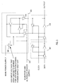
- FIG. 3 is an embodiment that highlights a register having a master portion 302, a slave portion 304, and a data retention portion 306 that is used in a power savings mode.
- the register illustrates the use of resource sharing of scan path 202 to allow the alternative power supply delivery channel to provide power to the data retention portion 306 when wireless communications device 10 is not operating in the test mode.
- scan path 202 delivers the original scan select signal in the test mode that selects the scan input of the registers for scan shifting, but highlighted in this figure is the use of scan path 202 to deliver the alternative power supply to the register when wireless communications device 10 is not operating in the test mode.
- the inverters/buffers located in master portion 302 and slave portion 304 are powered by the main power supply, whereas the inverters/buffers located in data retention portion 306 are powered by the alternative power supply delivered by scan path 202.
- the master portion 302 latches a value received at the DATA input in accordance with the CLOCK signal.
- the latched value from master portion 302 is passed to the slave portion 304 upon the appropriate transition of the CLOCK signal.
- the register is able to capture a DATA value in master portion 302 that is latched and stored in slave portion 304.
- wireless communications device 10 enters the power savings mode, the main power supply to master portion 302 and slave portion 304 is switched off.
- the inverters/buffers in master portion 302 and slave portion 304 are not powered.
- the data retention portion 306 is powered using the alternate power supply received on scan path 202 to retain the data value transferred from slave portion 304 upon entering the power savings mode.
- data retention portion 306 restores the data value to the slave portion 304 of the register prior to switching on the main power supply to master portion 302 and slave portion 304.
- the alternative power supply delivered to the combinatorial logic via scan path 202 allows the main power supply to shut down in the power savings mode to conserve power.
- the embodiment illustrated in the figure is an implementation choice for a retention logic design, but other latch circuits and retention logic circuits are anticipated.
- Scan path 202 is first turned on transitioning to a high potential to power up the retention portion 306.
- Data stored in slave portion 304 may be maintained in the slave portion until the main power is switched off.
- a high input voltage trip point inverter 308 detects that the main power supply is being shut off.
- trip point inverter 308 enables carlier isolation of the power regimes, i.e., the alternate power supply found in data retention portion 306 from the main power supply found in master portion 302 and slave portion 304.
- Trip point inverter 308 also has a high input voltage trip point to enable late detection of the main power switching on to ensure that slave portion 304 is able to retain the data value from the data retention portion 306 before tri-stating buffer 310.
- the proper sequence includes providing the alternative power supply to data retention portion 306 on scan path 202 prior to shutting off the main power supply to slave portion 304.
- the alternative power supply is provided to data retention portion 306 until the main power is restored and able to sustain the data value in slave portion 304 (but before the main power reaches a normal operational voltage level).
- Embodiments of the present invention allow the sharing of an existing test signal routing trace with an alternative power supply delivery to portions of the registers.
- Embodiments of the present invention allow silicon debugging by shifting the register value out in the middle of an operation, then resuming the operation after the scan shift operation.
Landscapes
- Engineering & Computer Science (AREA)
- Power Engineering (AREA)
- General Engineering & Computer Science (AREA)
- Physics & Mathematics (AREA)
- General Physics & Mathematics (AREA)
- Tests Of Electronic Circuits (AREA)
- Power Sources (AREA)
- Transceivers (AREA)
- Maintenance And Management Of Digital Transmission (AREA)
- Semiconductor Integrated Circuits (AREA)
Claims (10)
- Schaltung umfassend:ein Register, das mit einem Testsignal-Leitungsweg verbunden ist und mindestens einen ersten Abschnitt (302, 304) und einen zweiten Abschnitt (306) aufweist, wobei vom ersten oder zweiten Abschnitt einer (302, 304) abzuschalten ist, während die Hauptenergieversorgung abgeschaltet ist, undeine kombinatorische Logik, die mit dem Testsignal-Leitungsweg verbunden ist und dazu dient, während eines Testmodus über den Testsignal-Leitungsweg ein Testsignal zur Verfügung zu stellen,gekennzeichnet durch:einen Hocheingangsspannungs-Schaltpunkt-Inverter (308) mit Früh- und Späterfassung, um zu erfassen, ob eine Hauptenergieversorgung abgeschaltet oder angeschaltet wird,wobei die kombinatorische Logik (200) eingerichtet ist, in Antwort auf die Erfassung durch den Hocheingangsspannungs-Schaltpunkt-Inverter (308), dass die Hauptenergieversorgung abgeschaltet wird, dem Register über den Testsignal-Leitungsweg eine alternative Energieversorgung zur Verfügung zu stellen, und wobeivom ersten oder zweiten Registerabschnitt der andere (306) eingerichtet ist, durch den Testsignal-Leitungsweg (202) von der alternativen Energieversorgung mit Energie versorgt zu werden, während die Hauptenergieversorgung abgeschaltet ist.
- Schaltung nach Anspruch 1, wobei das Register einen Master/Slave-Abschnitt (302, 304), der zur Energieversorgung durch die Hauptenergieversorgung eingerichtet ist, und einen Niedrigenergie-Datenhalteabschnitt (306) aufweist, der mit dem Testsignal-Leitungsweg verbunden ist, um die alternative Energieversorgung anzunehmen.
- Schaltung nach Anspruch 2, wobei der Master/Slave-Abschnitt (302, 304) des Registers eingerichtet ist, einen Datenwert an den Niedrigenergie-Datenhalteabschnitt zu übertragen, wenn der Hocheingangsspannungs-Schaltpunkt-Inverter (308) erfasst, dass die Hauptenergieversorgung abgeschaltet oder angeschaltet wird.
- Schaltung nach Anspruch 3, wobei der Niedrigenergie-Datenhalteabschnitt (306) des Registers eingerichtet ist, den Datenwert an den Master/Slave-Abschnitt (302, 304) zu übertragen, wenn die Hauptenergieversorgung wiederhergestellt ist.
- Schaltung nach Anspruch 2, wobei ein Ausgang des Hocheingangsspannungs-Schaltpunkt-Inverters (308) tri-state gesetzt wird, um die alternative Energieversorgung von der Hauptenergieversorgung zu isolieren.
- Verfahren zum gemeinsamen Nutzen eines Scanpfads für zwei Zwecke, umfassend:Bereitstellen eines Auswahlsignals an einem Scaneingang eines Registers zum Scan-Schieben während eines Testmodus, wobei das Auswahlsignal über einen mit dem Scaneingang des Registers verbundenen Scanpfad (202) bereitgestellt wird,gekennzeichnet durchBereitstellen eines alternativen Energiepotenzials am Register über den Scanpfad, wenn das Register nicht im Testmodus betrieben wird,wobei das Register mindestens einen ersten Abschnitt (302, 304) und einen zweiten Abschnitt (306) umfassen soll und vom ersten oder zweiten Abschnitt einer (302, 304) während eines Niedrigenergiemodus abgeschaltet werden soll und vom ersten oder zweiten Abschnitt der andere (306) während des Niedrigenergiemodus über den Scanpfad (202) mittels des alternativen Energiepotenzials mit Energie versorgt werden soll.
- Verfahren nach Anspruch 6, weiterhin umfassend:Versorgen eines Master/Slave-Abschnitts (302, 304) des Registers mit Energie von einem Hauptenergiepotenzial, undVersorgen eines Niedrigenergie-Datenhalteabschnitts (306) des Registers über den Scanpfad (202) mit Energie von dem alternativen Energiepotenzial.
- Verfahren nach Anspruch 7, weiterhin umfassend:Verwenden eines Schaltpunkt-Inverters (308), um zu erfassen, dass das dem Register zugeführte Hauptenergiepotenzial abgeschaltet wird, und um unter Verwendung des Scanpfads (202) das alternative Energiepotenzial für das Register freizugeben.
- Verfahren nach Anspruch 8, weiterhin umfassend: Übertragen eines Datenwerts vom Master/Slave-Abschnitt des Registers (302, 304) an den Niedrigenergie-Datenhalteabschnitt (306), wenn der Schaltpunkt-Inverter erfasst, dass das Hauptenergiepotenzial abgeschaltet wird.
- Verfahren nach Anspruch 9, weiterhin umfassend: Übertragen des Datenwerts vom Niedrigenergie-Datenhalteabschnitt (306) des Registers an den Master/Slave-Abschnitt (302, 304), wenn das Hauptenergiepotenzial wiederhergestellt ist.
Applications Claiming Priority (2)
| Application Number | Priority Date | Filing Date | Title |
|---|---|---|---|
| US11/726,765 US7644328B2 (en) | 2007-03-22 | 2007-03-22 | Sharing routing of a test signal with an alternative power supply to combinatorial logic for low power design |
| PCT/US2008/057529 WO2008118717A1 (en) | 2007-03-22 | 2008-03-19 | Sharing routing of a test signal with an alternative power supply to combinatorial logic for low power design |
Publications (3)
| Publication Number | Publication Date |
|---|---|
| EP2143111A1 EP2143111A1 (de) | 2010-01-13 |
| EP2143111A4 EP2143111A4 (de) | 2010-08-25 |
| EP2143111B1 true EP2143111B1 (de) | 2013-04-24 |
Family
ID=39788924
Family Applications (1)
| Application Number | Title | Priority Date | Filing Date |
|---|---|---|---|
| EP08744081.4A Not-in-force EP2143111B1 (de) | 2007-03-22 | 2008-03-19 | Geteiltes routing eines testsignals mit einer alternativen stromversorgung in eine kombinatorische logik für niedrigleistungsdesign |
Country Status (6)
| Country | Link |
|---|---|
| US (1) | US7644328B2 (de) |
| EP (1) | EP2143111B1 (de) |
| JP (1) | JP4874407B2 (de) |
| CN (1) | CN101636794B (de) |
| TW (1) | TWI400932B (de) |
| WO (1) | WO2008118717A1 (de) |
Families Citing this family (5)
| Publication number | Priority date | Publication date | Assignee | Title |
|---|---|---|---|---|
| US8407540B2 (en) * | 2009-07-06 | 2013-03-26 | Arm Limited | Low overhead circuit and method for predicting timing errors |
| CN102543209B (zh) * | 2010-12-31 | 2015-09-30 | 深圳市朗科科技股份有限公司 | 多通道闪存控制器的纠错装置、方法及多通道闪存控制器 |
| US9372811B2 (en) * | 2012-12-13 | 2016-06-21 | Arm Limited | Retention priority based cache replacement policy |
| CN105204999B (zh) * | 2015-10-08 | 2017-11-21 | 浪潮电子信息产业股份有限公司 | 一种实现自动化测试的方法 |
| CN112100957B (zh) * | 2020-11-17 | 2021-02-02 | 芯华章科技股份有限公司 | 用于调试逻辑系统设计的方法、仿真器、存储介质 |
Family Cites Families (22)
| Publication number | Priority date | Publication date | Assignee | Title |
|---|---|---|---|---|
| JPS63299548A (ja) * | 1987-05-29 | 1988-12-07 | Seiichi Miyazaki | デ−タ伝送装置 |
| US5157781A (en) * | 1990-01-02 | 1992-10-20 | Motorola, Inc. | Data processor test architecture |
| JPH05284080A (ja) * | 1992-04-03 | 1993-10-29 | Toshiba Corp | 無線電話装置 |
| JPH0946267A (ja) * | 1995-07-27 | 1997-02-14 | Nec Kansai Ltd | 無線通信機用高周波機器 |
| US5621340A (en) * | 1995-08-02 | 1997-04-15 | Rambus Inc. | Differential comparator for amplifying small swing signals to a full swing output |
| US5675540A (en) * | 1996-01-22 | 1997-10-07 | Micron Quantum Devices, Inc. | Non-volatile memory system having internal data verification test mode |
| JP3228875B2 (ja) * | 1996-06-27 | 2001-11-12 | 株式会社日立製作所 | 信号配線の接続テスト方法、テスト装置及びバウンダリスキャン対応のic |
| US6052006A (en) * | 1998-05-27 | 2000-04-18 | Advanced Micro Devices, Inc. | Current mirror triggered power-on-reset circuit |
| KR100625753B1 (ko) * | 1999-02-16 | 2006-09-20 | 후지쯔 가부시끼가이샤 | 테스트 모드 입력 회로를 구비한 반도체 장치 |
| US6437623B1 (en) * | 2001-02-13 | 2002-08-20 | International Business Machines Corporation | Data retention registers |
| US20030188241A1 (en) * | 2002-03-29 | 2003-10-02 | International Business Machines Corporation | CMOS low leakage power-down data retention mechanism |
| US6744291B2 (en) * | 2002-08-30 | 2004-06-01 | Atmel Corporation | Power-on reset circuit |
| JP2004279266A (ja) * | 2003-03-17 | 2004-10-07 | Toshiba Corp | ロジック回路およびその設計方法並びにテスト方法 |
| US6965261B2 (en) * | 2003-11-13 | 2005-11-15 | Texas Instruments Incorporated | Ultra low-power data retention latch |
| TWI235599B (en) * | 2004-01-16 | 2005-07-01 | Sunplus Technology Co Ltd | Device and method for transmitting hidden signal in boundary scan testing interface |
| US7227383B2 (en) * | 2004-02-19 | 2007-06-05 | Mosaid Delaware, Inc. | Low leakage and data retention circuitry |
| US7486153B2 (en) * | 2004-04-13 | 2009-02-03 | Nxp, B.V. | Circuit and method for controlling an oscillation loop |
| JP4408061B2 (ja) * | 2004-06-14 | 2010-02-03 | 株式会社図書館流通センター | Icタグを用いた図書館システムにおけるダイポール型アンテナによるicタグスキャンシステム |
| US7154317B2 (en) * | 2005-01-11 | 2006-12-26 | Arm Limited | Latch circuit including a data retention latch |
| KR100630740B1 (ko) * | 2005-03-03 | 2006-10-02 | 삼성전자주식회사 | 스캔 기능을 갖는 고속 펄스 기반의 리텐션 플립플롭 |
| US7123068B1 (en) * | 2005-04-01 | 2006-10-17 | Freescale Semiconductor, Inc. | Flip-flop circuit having low power data retention |
| WO2006138583A2 (en) * | 2005-06-15 | 2006-12-28 | Texas Instruments Incorporated | Sequential scan test of interface between ic modules that operate at different frequencies |
-
2007
- 2007-03-22 US US11/726,765 patent/US7644328B2/en not_active Expired - Fee Related
-
2008
- 2008-03-19 EP EP08744081.4A patent/EP2143111B1/de not_active Not-in-force
- 2008-03-19 WO PCT/US2008/057529 patent/WO2008118717A1/en not_active Ceased
- 2008-03-19 CN CN200880009001.5A patent/CN101636794B/zh not_active Expired - Fee Related
- 2008-03-19 JP JP2009554718A patent/JP4874407B2/ja not_active Expired - Fee Related
- 2008-03-21 TW TW097110031A patent/TWI400932B/zh not_active IP Right Cessation
Also Published As
| Publication number | Publication date |
|---|---|
| US7644328B2 (en) | 2010-01-05 |
| JP2010521937A (ja) | 2010-06-24 |
| WO2008118717A1 (en) | 2008-10-02 |
| EP2143111A1 (de) | 2010-01-13 |
| CN101636794A (zh) | 2010-01-27 |
| TWI400932B (zh) | 2013-07-01 |
| US20080250280A1 (en) | 2008-10-09 |
| JP4874407B2 (ja) | 2012-02-15 |
| CN101636794B (zh) | 2014-04-23 |
| EP2143111A4 (de) | 2010-08-25 |
| TW200843464A (en) | 2008-11-01 |
Similar Documents
| Publication | Publication Date | Title |
|---|---|---|
| US6639454B2 (en) | Multiple circuit blocks with interblock control and power conservation | |
| US6794914B2 (en) | Non-volatile multi-threshold CMOS latch with leakage control | |
| EP1195902B1 (de) | Integrierte Halbleiterschaltung mit reduziertem Leckstrom | |
| US8289060B2 (en) | Pulsed state retention power gating flip-flop | |
| TWI546656B (zh) | 電源控制電路 | |
| US8363504B2 (en) | Device and method for state retention power gating | |
| US20100153759A1 (en) | Power gating technique to reduce power in functional and test modes | |
| US7644328B2 (en) | Sharing routing of a test signal with an alternative power supply to combinatorial logic for low power design | |
| WO2015069490A9 (en) | Methodology for testing integrated circuits | |
| JP5462703B2 (ja) | 順序回路におけるリーク電流の低減システム | |
| US20050050416A1 (en) | Scan chain modification for reduced leakage | |
| US7992024B2 (en) | Firewall/isolation cells for ultra low power products | |
| WO2006103484A1 (en) | System and method for reducing power consumption | |
| US10401931B2 (en) | Power delivery architecture to increase performance of computing systems when docked | |
| US20080155170A1 (en) | Utilization of scan structures and on-chip memory for retaining block state information during power down |
Legal Events
| Date | Code | Title | Description |
|---|---|---|---|
| PUAI | Public reference made under article 153(3) epc to a published international application that has entered the european phase |
Free format text: ORIGINAL CODE: 0009012 |
|
| 17P | Request for examination filed |
Effective date: 20090924 |
|
| AK | Designated contracting states |
Kind code of ref document: A1 Designated state(s): AT BE BG CH CY CZ DE DK EE ES FI FR GB GR HR HU IE IS IT LI LT LU LV MC MT NL NO PL PT RO SE SI SK TR |
|
| DAX | Request for extension of the european patent (deleted) | ||
| A4 | Supplementary search report drawn up and despatched |
Effective date: 20100726 |
|
| RIC1 | Information provided on ipc code assigned before grant |
Ipc: H03K 3/037 20060101AFI20100720BHEP Ipc: G11C 29/00 20060101ALI20100720BHEP Ipc: G01R 31/3185 20060101ALI20100720BHEP |
|
| 17Q | First examination report despatched |
Effective date: 20100806 |
|
| REG | Reference to a national code |
Ref country code: DE Ref legal event code: R079 Ref document number: 602008024091 Country of ref document: DE Free format text: PREVIOUS MAIN CLASS: G11C0029100000 Ipc: G11C0019280000 |
|
| RIC1 | Information provided on ipc code assigned before grant |
Ipc: G01R 31/3185 20060101ALI20120903BHEP Ipc: G11C 29/48 20060101ALI20120903BHEP Ipc: G11C 5/14 20060101ALI20120903BHEP Ipc: G11C 19/28 20060101AFI20120903BHEP |
|
| GRAP | Despatch of communication of intention to grant a patent |
Free format text: ORIGINAL CODE: EPIDOSNIGR1 |
|
| GRAS | Grant fee paid |
Free format text: ORIGINAL CODE: EPIDOSNIGR3 |
|
| GRAA | (expected) grant |
Free format text: ORIGINAL CODE: 0009210 |
|
| AK | Designated contracting states |
Kind code of ref document: B1 Designated state(s): AT BE BG CH CY CZ DE DK EE ES FI FR GB GR HR HU IE IS IT LI LT LU LV MC MT NL NO PL PT RO SE SI SK TR |
|
| REG | Reference to a national code |
Ref country code: GB Ref legal event code: FG4D |
|
| REG | Reference to a national code |
Ref country code: CH Ref legal event code: EP |
|
| REG | Reference to a national code |
Ref country code: AT Ref legal event code: REF Ref document number: 609045 Country of ref document: AT Kind code of ref document: T Effective date: 20130515 |
|
| REG | Reference to a national code |
Ref country code: IE Ref legal event code: FG4D |
|
| REG | Reference to a national code |
Ref country code: DE Ref legal event code: R096 Ref document number: 602008024091 Country of ref document: DE Effective date: 20130627 |
|
| REG | Reference to a national code |
Ref country code: AT Ref legal event code: MK05 Ref document number: 609045 Country of ref document: AT Kind code of ref document: T Effective date: 20130424 |
|
| REG | Reference to a national code |
Ref country code: LT Ref legal event code: MG4D |
|
| REG | Reference to a national code |
Ref country code: NL Ref legal event code: VDEP Effective date: 20130424 |
|
| PG25 | Lapsed in a contracting state [announced via postgrant information from national office to epo] |
Ref country code: PT Free format text: LAPSE BECAUSE OF FAILURE TO SUBMIT A TRANSLATION OF THE DESCRIPTION OR TO PAY THE FEE WITHIN THE PRESCRIBED TIME-LIMIT Effective date: 20130826 Ref country code: LT Free format text: LAPSE BECAUSE OF FAILURE TO SUBMIT A TRANSLATION OF THE DESCRIPTION OR TO PAY THE FEE WITHIN THE PRESCRIBED TIME-LIMIT Effective date: 20130424 Ref country code: FI Free format text: LAPSE BECAUSE OF FAILURE TO SUBMIT A TRANSLATION OF THE DESCRIPTION OR TO PAY THE FEE WITHIN THE PRESCRIBED TIME-LIMIT Effective date: 20130424 Ref country code: AT Free format text: LAPSE BECAUSE OF FAILURE TO SUBMIT A TRANSLATION OF THE DESCRIPTION OR TO PAY THE FEE WITHIN THE PRESCRIBED TIME-LIMIT Effective date: 20130424 Ref country code: BE Free format text: LAPSE BECAUSE OF FAILURE TO SUBMIT A TRANSLATION OF THE DESCRIPTION OR TO PAY THE FEE WITHIN THE PRESCRIBED TIME-LIMIT Effective date: 20130424 Ref country code: GR Free format text: LAPSE BECAUSE OF FAILURE TO SUBMIT A TRANSLATION OF THE DESCRIPTION OR TO PAY THE FEE WITHIN THE PRESCRIBED TIME-LIMIT Effective date: 20130725 Ref country code: ES Free format text: LAPSE BECAUSE OF FAILURE TO SUBMIT A TRANSLATION OF THE DESCRIPTION OR TO PAY THE FEE WITHIN THE PRESCRIBED TIME-LIMIT Effective date: 20130804 Ref country code: SE Free format text: LAPSE BECAUSE OF FAILURE TO SUBMIT A TRANSLATION OF THE DESCRIPTION OR TO PAY THE FEE WITHIN THE PRESCRIBED TIME-LIMIT Effective date: 20130424 Ref country code: NO Free format text: LAPSE BECAUSE OF FAILURE TO SUBMIT A TRANSLATION OF THE DESCRIPTION OR TO PAY THE FEE WITHIN THE PRESCRIBED TIME-LIMIT Effective date: 20130724 Ref country code: SI Free format text: LAPSE BECAUSE OF FAILURE TO SUBMIT A TRANSLATION OF THE DESCRIPTION OR TO PAY THE FEE WITHIN THE PRESCRIBED TIME-LIMIT Effective date: 20130424 Ref country code: IS Free format text: LAPSE BECAUSE OF FAILURE TO SUBMIT A TRANSLATION OF THE DESCRIPTION OR TO PAY THE FEE WITHIN THE PRESCRIBED TIME-LIMIT Effective date: 20130824 |
|
| PG25 | Lapsed in a contracting state [announced via postgrant information from national office to epo] |
Ref country code: CY Free format text: LAPSE BECAUSE OF FAILURE TO SUBMIT A TRANSLATION OF THE DESCRIPTION OR TO PAY THE FEE WITHIN THE PRESCRIBED TIME-LIMIT Effective date: 20130424 Ref country code: LV Free format text: LAPSE BECAUSE OF FAILURE TO SUBMIT A TRANSLATION OF THE DESCRIPTION OR TO PAY THE FEE WITHIN THE PRESCRIBED TIME-LIMIT Effective date: 20130424 Ref country code: BG Free format text: LAPSE BECAUSE OF FAILURE TO SUBMIT A TRANSLATION OF THE DESCRIPTION OR TO PAY THE FEE WITHIN THE PRESCRIBED TIME-LIMIT Effective date: 20130724 Ref country code: HR Free format text: LAPSE BECAUSE OF FAILURE TO SUBMIT A TRANSLATION OF THE DESCRIPTION OR TO PAY THE FEE WITHIN THE PRESCRIBED TIME-LIMIT Effective date: 20130424 Ref country code: PL Free format text: LAPSE BECAUSE OF FAILURE TO SUBMIT A TRANSLATION OF THE DESCRIPTION OR TO PAY THE FEE WITHIN THE PRESCRIBED TIME-LIMIT Effective date: 20130424 |
|
| PG25 | Lapsed in a contracting state [announced via postgrant information from national office to epo] |
Ref country code: EE Free format text: LAPSE BECAUSE OF FAILURE TO SUBMIT A TRANSLATION OF THE DESCRIPTION OR TO PAY THE FEE WITHIN THE PRESCRIBED TIME-LIMIT Effective date: 20130424 Ref country code: SK Free format text: LAPSE BECAUSE OF FAILURE TO SUBMIT A TRANSLATION OF THE DESCRIPTION OR TO PAY THE FEE WITHIN THE PRESCRIBED TIME-LIMIT Effective date: 20130424 Ref country code: DK Free format text: LAPSE BECAUSE OF FAILURE TO SUBMIT A TRANSLATION OF THE DESCRIPTION OR TO PAY THE FEE WITHIN THE PRESCRIBED TIME-LIMIT Effective date: 20130424 Ref country code: CZ Free format text: LAPSE BECAUSE OF FAILURE TO SUBMIT A TRANSLATION OF THE DESCRIPTION OR TO PAY THE FEE WITHIN THE PRESCRIBED TIME-LIMIT Effective date: 20130424 |
|
| PG25 | Lapsed in a contracting state [announced via postgrant information from national office to epo] |
Ref country code: NL Free format text: LAPSE BECAUSE OF FAILURE TO SUBMIT A TRANSLATION OF THE DESCRIPTION OR TO PAY THE FEE WITHIN THE PRESCRIBED TIME-LIMIT Effective date: 20130424 Ref country code: IT Free format text: LAPSE BECAUSE OF FAILURE TO SUBMIT A TRANSLATION OF THE DESCRIPTION OR TO PAY THE FEE WITHIN THE PRESCRIBED TIME-LIMIT Effective date: 20130424 Ref country code: RO Free format text: LAPSE BECAUSE OF FAILURE TO SUBMIT A TRANSLATION OF THE DESCRIPTION OR TO PAY THE FEE WITHIN THE PRESCRIBED TIME-LIMIT Effective date: 20130424 |
|
| PLBE | No opposition filed within time limit |
Free format text: ORIGINAL CODE: 0009261 |
|
| STAA | Information on the status of an ep patent application or granted ep patent |
Free format text: STATUS: NO OPPOSITION FILED WITHIN TIME LIMIT |
|
| 26N | No opposition filed |
Effective date: 20140127 |
|
| REG | Reference to a national code |
Ref country code: DE Ref legal event code: R097 Ref document number: 602008024091 Country of ref document: DE Effective date: 20140127 |
|
| PG25 | Lapsed in a contracting state [announced via postgrant information from national office to epo] |
Ref country code: LU Free format text: LAPSE BECAUSE OF FAILURE TO SUBMIT A TRANSLATION OF THE DESCRIPTION OR TO PAY THE FEE WITHIN THE PRESCRIBED TIME-LIMIT Effective date: 20140319 |
|
| REG | Reference to a national code |
Ref country code: CH Ref legal event code: PL |
|
| REG | Reference to a national code |
Ref country code: FR Ref legal event code: ST Effective date: 20141128 |
|
| REG | Reference to a national code |
Ref country code: IE Ref legal event code: MM4A |
|
| PG25 | Lapsed in a contracting state [announced via postgrant information from national office to epo] |
Ref country code: FR Free format text: LAPSE BECAUSE OF NON-PAYMENT OF DUE FEES Effective date: 20140331 Ref country code: LI Free format text: LAPSE BECAUSE OF NON-PAYMENT OF DUE FEES Effective date: 20140331 Ref country code: IE Free format text: LAPSE BECAUSE OF NON-PAYMENT OF DUE FEES Effective date: 20140319 Ref country code: CH Free format text: LAPSE BECAUSE OF NON-PAYMENT OF DUE FEES Effective date: 20140331 |
|
| PG25 | Lapsed in a contracting state [announced via postgrant information from national office to epo] |
Ref country code: MT Free format text: LAPSE BECAUSE OF FAILURE TO SUBMIT A TRANSLATION OF THE DESCRIPTION OR TO PAY THE FEE WITHIN THE PRESCRIBED TIME-LIMIT Effective date: 20130424 |
|
| PG25 | Lapsed in a contracting state [announced via postgrant information from national office to epo] |
Ref country code: MC Free format text: LAPSE BECAUSE OF FAILURE TO SUBMIT A TRANSLATION OF THE DESCRIPTION OR TO PAY THE FEE WITHIN THE PRESCRIBED TIME-LIMIT Effective date: 20130424 |
|
| PG25 | Lapsed in a contracting state [announced via postgrant information from national office to epo] |
Ref country code: HU Free format text: LAPSE BECAUSE OF FAILURE TO SUBMIT A TRANSLATION OF THE DESCRIPTION OR TO PAY THE FEE WITHIN THE PRESCRIBED TIME-LIMIT; INVALID AB INITIO Effective date: 20080319 Ref country code: TR Free format text: LAPSE BECAUSE OF FAILURE TO SUBMIT A TRANSLATION OF THE DESCRIPTION OR TO PAY THE FEE WITHIN THE PRESCRIBED TIME-LIMIT Effective date: 20130424 |
|
| PGFP | Annual fee paid to national office [announced via postgrant information from national office to epo] |
Ref country code: DE Payment date: 20200303 Year of fee payment: 13 Ref country code: GB Payment date: 20200311 Year of fee payment: 13 |
|
| REG | Reference to a national code |
Ref country code: DE Ref legal event code: R119 Ref document number: 602008024091 Country of ref document: DE |
|
| GBPC | Gb: european patent ceased through non-payment of renewal fee |
Effective date: 20210319 |
|
| PG25 | Lapsed in a contracting state [announced via postgrant information from national office to epo] |
Ref country code: GB Free format text: LAPSE BECAUSE OF NON-PAYMENT OF DUE FEES Effective date: 20210319 Ref country code: DE Free format text: LAPSE BECAUSE OF NON-PAYMENT OF DUE FEES Effective date: 20211001 |