EP2141511A2 - Radiation detector using gas amplication and method for manufacturing the same - Google Patents
Radiation detector using gas amplication and method for manufacturing the same Download PDFInfo
- Publication number
- EP2141511A2 EP2141511A2 EP09163506A EP09163506A EP2141511A2 EP 2141511 A2 EP2141511 A2 EP 2141511A2 EP 09163506 A EP09163506 A EP 09163506A EP 09163506 A EP09163506 A EP 09163506A EP 2141511 A2 EP2141511 A2 EP 2141511A2
- Authority
- EP
- European Patent Office
- Prior art keywords
- electrode pattern
- convex portions
- electrode
- insulating member
- solder material
- Prior art date
- Legal status (The legal status is an assumption and is not a legal conclusion. Google has not performed a legal analysis and makes no representation as to the accuracy of the status listed.)
- Granted
Links
- 230000005855 radiation Effects 0.000 title claims abstract description 67
- 238000004519 manufacturing process Methods 0.000 title claims description 26
- 238000000034 method Methods 0.000 title claims description 10
- 239000000463 material Substances 0.000 claims abstract description 96
- 229910000679 solder Inorganic materials 0.000 claims abstract description 94
- 230000003321 amplification Effects 0.000 claims abstract description 14
- 238000003199 nucleic acid amplification method Methods 0.000 claims abstract description 14
- 238000007747 plating Methods 0.000 claims description 22
- 239000011248 coating agent Substances 0.000 claims description 8
- 238000000576 coating method Methods 0.000 claims description 8
- 238000005530 etching Methods 0.000 claims description 4
- 230000001678 irradiating effect Effects 0.000 claims description 3
- 238000010891 electric arc Methods 0.000 description 18
- 230000005684 electric field Effects 0.000 description 14
- 230000035945 sensitivity Effects 0.000 description 13
- 238000001514 detection method Methods 0.000 description 10
- 230000015572 biosynthetic process Effects 0.000 description 6
- 239000000758 substrate Substances 0.000 description 5
- CURLTUGMZLYLDI-UHFFFAOYSA-N Carbon dioxide Chemical compound O=C=O CURLTUGMZLYLDI-UHFFFAOYSA-N 0.000 description 4
- VNWKTOKETHGBQD-UHFFFAOYSA-N methane Chemical compound C VNWKTOKETHGBQD-UHFFFAOYSA-N 0.000 description 4
- RYGMFSIKBFXOCR-UHFFFAOYSA-N Copper Chemical compound [Cu] RYGMFSIKBFXOCR-UHFFFAOYSA-N 0.000 description 2
- PXHVJJICTQNCMI-UHFFFAOYSA-N Nickel Chemical compound [Ni] PXHVJJICTQNCMI-UHFFFAOYSA-N 0.000 description 2
- ATJFFYVFTNAWJD-UHFFFAOYSA-N Tin Chemical compound [Sn] ATJFFYVFTNAWJD-UHFFFAOYSA-N 0.000 description 2
- 229910002092 carbon dioxide Inorganic materials 0.000 description 2
- 239000001569 carbon dioxide Substances 0.000 description 2
- 239000004020 conductor Substances 0.000 description 2
- 229910052802 copper Inorganic materials 0.000 description 2
- 239000010949 copper Substances 0.000 description 2
- 230000003247 decreasing effect Effects 0.000 description 2
- 230000000694 effects Effects 0.000 description 2
- 150000002500 ions Chemical class 0.000 description 2
- 239000011347 resin Substances 0.000 description 2
- 229920005989 resin Polymers 0.000 description 2
- 229920001187 thermosetting polymer Polymers 0.000 description 2
- 229910017944 Ag—Cu Inorganic materials 0.000 description 1
- 229910020220 Pb—Sn Inorganic materials 0.000 description 1
- 239000004642 Polyimide Substances 0.000 description 1
- BQCADISMDOOEFD-UHFFFAOYSA-N Silver Chemical compound [Ag] BQCADISMDOOEFD-UHFFFAOYSA-N 0.000 description 1
- 229910020830 Sn-Bi Inorganic materials 0.000 description 1
- 229910020888 Sn-Cu Inorganic materials 0.000 description 1
- 229910020994 Sn-Zn Inorganic materials 0.000 description 1
- 229910018728 Sn—Bi Inorganic materials 0.000 description 1
- 229910019204 Sn—Cu Inorganic materials 0.000 description 1
- 229910009069 Sn—Zn Inorganic materials 0.000 description 1
- 230000002378 acidificating effect Effects 0.000 description 1
- 229910052782 aluminium Inorganic materials 0.000 description 1
- XAGFODPZIPBFFR-UHFFFAOYSA-N aluminium Chemical compound [Al] XAGFODPZIPBFFR-UHFFFAOYSA-N 0.000 description 1
- 230000002547 anomalous effect Effects 0.000 description 1
- 238000007664 blowing Methods 0.000 description 1
- 230000015556 catabolic process Effects 0.000 description 1
- 239000013078 crystal Substances 0.000 description 1
- 230000007547 defect Effects 0.000 description 1
- 230000001419 dependent effect Effects 0.000 description 1
- 230000000994 depressogenic effect Effects 0.000 description 1
- 230000003292 diminished effect Effects 0.000 description 1
- 238000007772 electroless plating Methods 0.000 description 1
- PCHJSUWPFVWCPO-UHFFFAOYSA-N gold Chemical compound [Au] PCHJSUWPFVWCPO-UHFFFAOYSA-N 0.000 description 1
- 229910052737 gold Inorganic materials 0.000 description 1
- 239000010931 gold Substances 0.000 description 1
- 238000010438 heat treatment Methods 0.000 description 1
- 238000002844 melting Methods 0.000 description 1
- 230000008018 melting Effects 0.000 description 1
- 230000004048 modification Effects 0.000 description 1
- 238000012986 modification Methods 0.000 description 1
- 229910052759 nickel Inorganic materials 0.000 description 1
- 229920001721 polyimide Polymers 0.000 description 1
- 230000002265 prevention Effects 0.000 description 1
- 229910052709 silver Inorganic materials 0.000 description 1
- 239000004332 silver Substances 0.000 description 1
Images


Classifications
-
- G—PHYSICS
- G01—MEASURING; TESTING
- G01T—MEASUREMENT OF NUCLEAR OR X-RADIATION
- G01T1/00—Measuring X-radiation, gamma radiation, corpuscular radiation, or cosmic radiation
- G01T1/16—Measuring radiation intensity
- G01T1/185—Measuring radiation intensity with ionisation chamber arrangements
-
- Y—GENERAL TAGGING OF NEW TECHNOLOGICAL DEVELOPMENTS; GENERAL TAGGING OF CROSS-SECTIONAL TECHNOLOGIES SPANNING OVER SEVERAL SECTIONS OF THE IPC; TECHNICAL SUBJECTS COVERED BY FORMER USPC CROSS-REFERENCE ART COLLECTIONS [XRACs] AND DIGESTS
- Y10—TECHNICAL SUBJECTS COVERED BY FORMER USPC
- Y10T—TECHNICAL SUBJECTS COVERED BY FORMER US CLASSIFICATION
- Y10T29/00—Metal working
- Y10T29/49—Method of mechanical manufacture
- Y10T29/49002—Electrical device making
- Y10T29/49117—Conductor or circuit manufacturing
- Y10T29/49124—On flat or curved insulated base, e.g., printed circuit, etc.
- Y10T29/49155—Manufacturing circuit on or in base
- Y10T29/49156—Manufacturing circuit on or in base with selective destruction of conductive paths
Definitions
- the present invention relates to a radiation detector with a pixel electrode using gas amplification and a method for manufacturing the radiation detector.
- a pixel radiation detector would be employed as a radiation detector using gas amplification.
- a strip cathode electrode is formed on the main surface of a double-sided printed substrate and a strip anode electrode is formed on the rear surface of the same printed substrate while openings are formed in the strip cathode electrode at a constant pitch and columnar anode electrodes are protruded at the centers of the respective openings, the columnar electrodes being electrically connected with the strip anode electrode.
- the columnar electrodes constitute the pixel electrode of the pixel radiation detector.
- the radiation detector is disposed in an atmosphere containing He gas and methane gas. Then, a voltage of 600 V is applied between the pixel electrode and the strip cathode electrode, for example.
- the gas is ionized to generate electrons. Since a large voltage is applied between the strip cathode electrode and the pixel electrode such that an electric field with a high intensity is generated due to the configuration of point electrode of the pixel electrode (i.e., the shape anisotropy of the pixel electrode) , electron avalanche amplification is brought about. On the other hand, the positive ions generated by the electron avalanche amplification are drifted to the corresponding approximate edges of the strip cathode electrode from the pixel electrode (i.e., the columnar electrodes).
- the intensity of the electric field to be generated is increased so that the electron avalanche amplification is brought about remarkably.
- the detection sensitivity of the radiation can be also increased.
- a large voltage is applied to the pixel electrode, particularly, arc discharge occurs between the pixel electrode and the edges exposing to the corresponding openings of the strip cathode electrode so as to damage the strip cathode electrode and the pixel electrode.
- the arc discharge occurs so that the radiation detector can not function so that the detection sensitivity of the radiation detector is enhanced.
- the pixel electrode i.e., the columnar electrodes
- enhance the intensity of the electric field to be generated instead of to control the voltage to be applied to the pixel electrode.
- the pixel electrode is configured such that the through holes formed in the printed substrate are embedded by means of via-fill plating, it is required to narrow the through holes in order to narrow the pixel electrode.
- the via-fill plating can not be uniformly carried out for the through holes so that the pixel electrode can not be also formed uniformly. In this case, anomalous discharge and dielectric breakdown disadvantageously occur. Therefore, the narrowing of the pixel electrode is restricted spontaneously in dependence on the forming method.
- the voltage to be applied to the pixel electrode can not be sufficiently developed while the narrowing of the pixel electrode can not be sufficiently realized, so that the detection sensitivity of the pixel radiation detector can not be sufficiently enhanced.
- the present invention relates to a radiation detector using gas amplification, including: a first electrode pattern which is formed on a first surface of an insulating member and has a plurality of circular openings; and a second electrode pattern which is formed on a second surface of the insulating member opposite to the first surface thereof and has convex portions of which respective forefronts are exposed to centers of the openings of the first electrode pattern; wherein a predetermined electric potential is set between the first electrode pattern and the second electrode pattern; wherein edges of the first electrode pattern exposed to the openings are shaped in respective continuous first curved surfaces by covering the edges thereof with a first solder material.
- the present invention also relates to a method for manufacturing a radiation detector using gas amplification, comprising the steps of : forming a first electrode layer on a first surface of an insulating member and forming a second electrode layer on a second surface of the insulating member opposite to the second surface thereof; conducting a first treatment including resist coating, exposing, developing and etching for the first electrode layer to form a plurality of openings for processing at the first electrode layer; irradiating an energy beam onto the insulating member via the plurality of openings for processing formed at the first electrode layer or conducting a second treatment including resist coating, exposing and developing when the insulating member is a photosensitive insulating member to form through holes at the insulating member in a thickness direction of the insulating member; conducting via-fill plating into the through holes to form metallic plating layers so as to embed the through holes; conducting the first treatment for the first electrode layer to form a plurality of circular openings such that the metallic plating members are disposed at centers of the circular openings, respectively
- the inventors studied intensely so as to achieve the object of the present invention. As a result, the inventors found out the following fact.
- a voltage of e.g. , 500 V to 700 V is applied between the pixel electrode made of the convex portions of the second electrode pattern and the strip cathode electrode made of the first electrode pattern, the thus generated electric field is concentrated onto the rectangular edges of the strip cathode electrode which is exposed to the corresponding openings so that arc discharge occurs between the pixel electrode and the strip cathode electrode.
- the first solder material is formed on the first electrode pattern constituting the strip cathode electrode and reflowed so as to cover the edges exposing to the corresponding openings of the first electrode pattern and thus, shape the edges thereof in respective continuous first curved surfaces. Therefore, if a large voltage is applied between the first electrode pattern and the convex portions of the second electrode pattern, that is, between the pixel electrode and the strip cathode electrode, the thus generated electric field can not be locally concentrated because the edges of the first electrode pattern are shaped so as to have the respective curved surfaces.
- the radiation detector can exhibit a high detection sensitivity due to the application of the large voltage therebetween.
- a second solder material is formed and reflowed on the convex portions of the second electrode such that the convex portions of the second electrode pattern are shaped in respective continuous second curved surfaces by covering the convex portions with the second solder material.
- the electric field is likely to be concentrated onto the protrusions of the pixel electrode so that arc discharge is likely to occur between the protrusions of the pixel electrode and the edges of the strip cathode electrodes.
- the surface state of the pixel electrode i.e., the protrusions thereof
- the surface state of the pixel electrode can be shaped in a continuous curved surface by covering the convex portions of the second electrode pattern with a solder material so that the local electric concentration of the electric field for the pixel electrode can be prevented.
- the radiation detector can exhibit a high detection sensitivity due to the high voltage to be applied.
- continuous first curved surface and “continuous second curved surface” mean that the surface state is smooth without local deformation such as protrusion and depressed portion from the starting point of the surface to the ending point thereof.
- the edges of the first electrode pattern as the strip cathode electrode are shaped in curved surfaces respectively and/or the convex portions of the second electrode pattern as the pixel electrode are shaped in hemispherical surfaces respectively, the curved surfaces being curved outward from the corresponding edges of the first electrode pattern and the hemispherical surfaces being curved outward, the curvatures of the curved surfaces and the hemispherical surfaces become large, so that the electric concentration for the edges of the first electrode pattern and/or the convex portions of the second electrode pattern can be prevented, thereby suppressing the arc discharge at the edges thereof and/or the convex portions thereof effectively and efficiently.
- the radiation detector can absolutely exhibit a high detection sensitivity dependent on the amplitude of the voltage to be applied.
- the electric concentration of the electric field on the protrusions and the like can be suppressed by covering the convex portions of the second electrode pattern as the pixel electrode with a solder material even though the edges of the first electrode pattern are not covered with a solder material, so that the arc discharge between the convex portions of the second electrode pattern as the pixel electrode and the edges of the first electrode pattern as the strip cathode electrode can be suppressed.
- a new pixel radiation detector which has a sufficiently higher detection sensitivity and a method for manufacturing the new pixel radiation detector.
- Fig. 1 is a plan view schematically showing the structure of the radiation detector according to an embodiment of the present invention.
- Fig. 2 is a perspective view enlargedly showing the pixel radiation detector of the radiation detector shown in Fig. 1 .
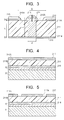
- Fig. 3 is a cross sectional view enlargedly showing the area around the pixel electrode of the pixel radiation detector.
- Fig. 4 is a cross sectional view showing one step of the manufacturing method according to an embodiment of the present invention.
- Fig. 5 is also a cross sectional view showing one step of the manufacturing method according to an embodiment of the present invention.
- Fig. 6 is also a cross sectional view showing one step of the manufacturing method according to an embodiment of the present invention.
- Fig. 7 is also a cross sectional view showing one step of the manufacturing method according to an embodiment of the present invention.
- Fig. 8 is also a cross sectional view showing one step of the manufacturing method according to an embodiment of the present invention.
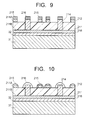
- Fig. 9 is also a cross sectional view showing one step of the manufacturing method according to an embodiment of the present invention.
- Fig. 10 is also a cross sectional view showing one step of the manufacturing method according to an embodiment of the present invention.
- Fig. 1 is a plan view schematically showing the structure of the radiation detector according to an embodiment of the present invention.
- Fig. 2 is a perspective view enlargedly showing the pixel radiation detector of the radiation detector shown in Fig. 1 .
- Fig. 3 is a cross sectional view enlargedly showing the area around the pixel electrode of the pixel radiation detector.
- a radiation detector 10 in this embodiment includes a pixel radiation detector 20 and a current detecting circuit (not shown).
- the pixel radiation detector 20 includes a detecting panel 21 and an electrode plate 22 which is provided above the detecting panel 21 so as to be opposite thereto.
- the detecting panel 21 includes a first electrode pattern 212 with a plurality of circular openings 212A which is formed on the main surface 211A of an insulating member 211 and a second electrode pattern 213 formed on the rear surface 211B of the insulating member 211.
- the second electrode pattern 213 includes convex portions 214 which are formed through the insulating member 211 and of which the forefronts are exposed almost at the centers of the openings 212A of the first electrode pattern 212, respectively.
- the convex portions 214 constitute a pixel electrode.
- a first solder material 215 is formed on the first electrode pattern 212 and melted through the reflow thereof so that the edges of the first solder material 215 exposing to the corresponding openings 212A can be shaped in respective curved surfaces, the curved surfaces being curved outward from the edges of the first electrode pattern 212 exposing to the corresponding openings 212A.
- a second solder material is formed over the convex portions 214 of the second electrode pattern 213 and melted through the reflow thereof so that the top surfaces of the convex portions can be shaped in respective hemispherical surfaces, the hemispherical surfaces being curved outward.
- the curvature of the first solder material 215 at each edge 215A is preferably set so as to satisfy the relation of 0.3 ⁇ r/t2 ⁇ 1.25 if the curvature radius of the curvature of the first solder material 215 at each edge 215A is defined as "r” and the thickness of the first electrode pattern 212 is defined as "t2".
- the curvature of the second solder material 216 is preferably set so as to satisfy the relation of 0.07 ⁇ R/d ⁇ 0.25 if the curvature radius of the curvature of the second solder material 216 is defined as "R" and the diameter of each of the convex portions 214 is defined as "d”.
- the first solder material 215 at each edge 215A and the second solder material 216 at each convex portion 214 are shaped so as to have the respective loose curved (spherical) surfaces, so that arc discharge due to the electric field concentration can be effectively suppressed, as will be described below.
- the detecting panel 21 of the pixel radiation detector 20 shown in Fig. 2 eight openings 212A are formed at the first electrode pattern 211A in double row such that four openings 212A are arranged per row and in parallel. Moreover, the forefronts of the convex portions 214 are protruded from the corresponding openings 212A (the insulating portions located between the edges of the first electrode pattern (strip cathode electrode) exposing to the corresponding openings 212A and the pixel electrode (convex portions) such that eight detecting electrode can be formed.
- the number of the detecting electrode and the arrangement may be determined as occasion demands.
- the second electrode pattern 213 are also patterned in strip so as to be almost orthogonal to the arrangement direction of the first electrode pattern 212.
- the second electrode pattern 213 may be patterned in any direction not parallel to the arrangement direction of the first electrode pattern 212.
- the thickness "t1" of the insulating member 211 may be set within a range of 20 ⁇ m to 100 ⁇ m, for example.
- the thickness "t2" of the first electrode pattern 212 and the thickness “t3" of the second electrode pattern 213 may be set within a range of 5 ⁇ m to 18 ⁇ m, respectively.
- the height “L” of the convex portion 214 may be set to the summation of the thickness "t1" of the insulating member 211 and the thickness "t2" of the first electrode pattern 212.
- the diameter “D” of the opening 212A may be set within a range of 80 ⁇ m to 300 ⁇ m.
- the diameter "d" of the convex portion 214 may be set within a range of 15 ⁇ m to 70 ⁇ m.
- the curvature radius "r" of the first solder material 215 may be set within a range of 5 ⁇ m to 30 ⁇ m
- the curvature radius "R” of the second solder material 216 may be set within a range of 5 ⁇ m to 30 ⁇ m.
- the first electrode pattern 212 and the second electrode pattern 213 may be made of an electrically conductive material such as copper, gold, silver, nickel and aluminum.
- the insulating member 211 may be made of a thermosetting resin film or sheet.
- the first solder material 215 and the second solder material 216 may be made of a high-temperature Pb-free solder material such as a Sn-Cu or Sn-Ag-Cu based Pb-free solder material, a medium-temperature Pb-free solder material such as a Sn-Zn based Pb-free solder material or a Sn-Bi based Pb-free solder material in addition to a normal Pb-Sn based solder material.
- a high-temperature Pb-free solder material such as a Sn-Cu or Sn-Ag-Cu based Pb-free solder material
- a medium-temperature Pb-free solder material such as a Sn-Zn based Pb-free solder material or a Sn-Bi based Pb-free solder material in addition to a normal Pb-Sn based solder material.
- the first solder material 215 may be made of the same solder material as the second solder material 216.
- the first solder material 215 may be made of a different solder material from the second solder material 216. In the latter case, however, since the number of step for forming the solder materials is increased in the total manufacturing process for the intended radiation detector 10, the total number of step for manufacturing the radiation detector 10 is also increased. In this point view, the former case (the first solder material 215 is made of the same solder material as the second solder material 216) is preferable.
- a predetermined voltage e.g., within a range of 500 V to 700 V is applied between the first electrode pattern 212 and the second electrode pattern 213.
- the first electrode pattern 212 may be set as a cathode electrode and the second electrode pattern 213 may be set as an anode electrode.
- the first electrode pattern 212 may be set as an anode electrode and the second electrode pattern 213 may be set as a cathode electrode.
- the first electrode pattern 212 is set as a cathode electrode and the second electrode pattern 213 is set as an anode electrode. Therefore, the preferable example will be described hereinafter.
- a predetermined gas e.g., a mixed gas of He gas and methane gas is charged between the detecting panel 21 and the electrode plate 22.
- the electrode plate 22 is biased to a predetermined electric potential.
- the radiation collides with the atoms or molecules of the charged gas so that the charged gas (i.e., the atoms or molecules) is ionized to generate electrons.
- the thus generated electrons are introduced to the detecting panel 21 subject to the electric potential of the electrode plate 22 of the pixel radiation detector 20 so as to bring about the electron avalanche also subject to the high intensity electric field generated between the first electrode pattern 212 and the convex portions 214 of the second electrode pattern 213, the high intensity electric field being generated by the large voltage applied between the first electrode pattern 212 and the convex portions 214 of the second electrode pattern 213.
- the newly generated electrons are charged to the convex portions 214.
- the positive ions generated by the electron avalanche are drifted from the convex portions 214 to the corresponding edges of the first electrode pattern 212 in the vicinity of the convex portions 214.
- the input position of the radiation in the pixel radiation detector 20 can be specified by detecting the position of the charged convex portions 214, that is, the charged position of the pixel electrode with the electric charge detecting circuit (not shown) . In this way, the input radiation can be detected.
- the edges of the first electrode pattern 212 are covered with the first solder material 215 so as to have the respective curved surfaces (spherical surfaces) , the electric field can not be locally concentrated to the edges of the first electrode pattern 212.
- the large voltage is applied between the first electrode pattern 212 and the convex portions 214 of the second electrode pattern 213, that is, between the strip cathode electrode and the pixel electrode, no arc discharge can occur therebetween. Therefore, the radiation detector 20 can exhibit a high detecting sensitivity due to the application of the large voltage.
- the convex portions 214 of the second electrode pattern 213 are covered with the second solder material 216 so as to have the respective curved surfaces (spherical surfaces), the surface nonuniformity due to some protrusion formed on the surface of the second electrode pattern 213 can be diminished by the second solder material 216 even though the surface state of the second electrode pattern 213 becomes nonuniform due to the formation of the protrusions. Therefore, the arc discharge originated from the surface nonuniformity of the convex portions 214 of the second electrode pattern 213 can be prevented so that the radiation detector 20 can exhibit a high detecting sensitivity due to the application of the large voltage.
- the surface nonuniformity of the convex portions 214 of the second electrode pattern 213 is originated from the defects generated through the manufacturing process thereof, the surface nonuniformity can not be formed if the convex portions 214 of the second electrode pattern 213 are formed ideally. In this case, therefore, no arc discharge due to the surface nonuniformity occurs.
- the edges of the first electrode pattern 212 (located at the insulating portions between the strip cathode electrode and the pixel electrode) become rectangular as the first electrode pattern 212 is formed ideally so that arc discharge is likely to occur by the electric concentration of the electric field onto the edges thereof. Therefore, the edges of the first electrode pattern 212 firstly contribute to the occurrence of the arc discharge and the surface uniformity of the convex portions 214 of the second electrode pattern 213 secondly contribute the occurrence of the arc discharge.
- Figs. 4 to 10 relate to the steps of the manufacturing method.
- Figs. 4 to 10 are cross sectional views relating to the pixel radiation detector under manufacture, taken on line P-P.
- a first electrode layer 217 and a second electrode layer 218 are formed on the main surface 211A and the rear surface 211B of the insulating member 211.
- the insulating member 211 may be made of a thermosetting resin film or sheet, for example.
- the first electrode layer 217 and the second electrode layer 218 are made of an electrically conductive material such as copper.
- the second electrode layer 218 is adhered with a supporting substrate 31 made of, e.g., polyimide via a prepreg 32.
- the supporting substrate 31 and the prepreg 32 may be omitted.
- a first treatment including a set of subsequent resist coating, exposing, developing and etching is carried out for the first electrode layer 217 so that a plurality of openings 217A for processing are formed and simultaneously, the first electrode layer 217 is formed in strip shape.
- an energy beam is irradiated onto the insulating member 211 via the openings 217A for processing of the first electrode layer 217 to form through holes 211H in the thickness direction of the insulating member 211.
- a laser beam may be employed, for example.
- the carbon dioxide gas laser processes only the insulating member 211 and does not process the second electrode layer 218 due to the wavelength characteristics.
- a second treatment including a set of subsequent resist coating, exposing, and developing is carried out for the insulating member 211. In this case, the exposed portions of the insulating member 211 are melted and removed by the developing to form the through holes 211H.
- via-fill plating is carried out for the through holes 211H so that the through holes 211H are embedded by metallic plating layers 214.
- the first treatment is carried out for the first electrode layer 217 again so that the circular openings 212 are formed under the condition that the metallic plating layers 214 are disposed at the centers of the corresponding openings 212.
- the first electrode pattern 212 is formed and the second electrode pattern 213 made of the second electrode layer 218 and having the convex portions 214 made of the metallic plating layers 214 is formed.
- the first solder material 215 is formed over the first electrode pattern 212 and the second solder material 216 is formed on the convex portions 214 of the second electrode pattern 213.
- the first solder material 215 and the second solder material 216 are reflowed to be melted so that the first solder material 215 is formed at the edges of the first electrode pattern 212 in curved surface shape and the second solder material 216 is formed at the convex portions 214 in hemispherical surface shape, the curved surfaces at the edges of the first electrode pattern 212 being curved outward from the edges thereof and the hemispherical surfaces at the convex portions 214 being curved outward.
- HAL treatment may be employed in the formation of the first solder material 215 on the first electrode pattern 212 and the formation of the second solder material 216 on the convex portions 214 of the second electrode pattern 213.
- the HAL treatment is conducted using a plating apparatus for plating a solder called as hot air leveler.
- the laminated body shown in Fig. 8 is immersed in a solder bath containing a heated and melted solder material so that the solder materials are formed on the first electrode pattern 212 and the convex portions 214.
- the laminated body is pulled up from the solder bath, a hot air is blown to the laminated body such that the blowing direction of the hot air is orthogonal to the surfaces in the sides of the first electrode pattern 212 and the convex portions 214.
- the surface of the solder layer formed on the first electrode pattern 212 and the like can be smoothed and uniform in thickness.
- the first solder material 215 can be formed on the first electrode pattern 212 and the second solder material 216 can be formed on the convex portions 214.
- the first solder material 215 and the second solder material 216 are reflowed to be melted so that the first solder material 215 is formed at the edges of the first electrode pattern 212 in curved surface shape and the second solder material 216 is formed at the convex portions 214 in hemispherical surface shape, the curved surfaces at the edges of the first electrode pattern 212 being curved outward from the edges thereof and the hemispherical surfaces at the convex portions 214 being curved outward, as described above.
- the reflow of the solder materials causes the prevention of the occurrence of whisker crystal by the heating accompanied by the reflow of the solder materials in addition to the formation of the outwardly curved surfaces of the solder materials.
- the laminated body shown in Fig. 8 is immersed in an acidic tin plating bath, for example so that tin material is deposited as the solder materials on the first electrode pattern 212 and the convex portions 214 of the second electrode pattern 213.
- the first solder material 215 may be formed on the first electrode pattern 212 and the second solder material 216 may be formed on the convex portions 214 of the second electrode pattern 213.
- the detecting panel 21 is formed. Then, the electrode plate 22 is provided so as to be opposite to the detecting panel 21 and the mixed gas is charged while the casing is conducted to form the intended radiation detector as shown in Fig. 1 .
- the first solder material 215 is formed so as to have the curved surfaces at the edges of the first electrode pattern 212 and the second solder material 216 is formed so as to have the hemispherical surfaces at the convex portions 214 of the second electrode pattern 213.
- the first solder material 215 may be formed so as to have any shaped surfaces at the edges of the first electrode pattern 212 and the second solder material 216 may be formed so as to have any shaped surfaces at the convex portions 214 of the second electrode pattern 213.
- the first solder material 215 and the second solder material 216 are prepared and formed on both of the first electrode pattern 212 and the convex portions 214, but one solder material is prepared and formed either of the first electrode pattern 212 and the convex portions 214.
- the first solder material 215 is formed on the first electrode pattern 212, the primary arc discharge due to the edges of the first electrode pattern 212 can be prevented.
- the second solder material 216 is formed on the convex portions 214 of the second electrode pattern 213, the secondary arc discharge due to the surface uniformity of the second electrode pattern 213 can be prevented.
- the solder materials are employed such that the shapes of the edges of the first electrode pattern exposing to the corresponding openings are rendered in the respective curved surfaces and the shapes of the convex portions of the second electrode pattern are rendered in the respective curved surfaces(hemispherical surfaces) through the reflow of the solder materials.
- any material may be employed only if the material can have a melting point much lower than the material making the electrode and can be shaped so as to have a curved surface through the reflow thereof.
- solder materials are selected only because the solder materials are in existence and commercially available. Therefore, only if the above-described effect/function can be exhibited, another material may be employed which is available at present or in the future.
Landscapes
- Physics & Mathematics (AREA)
- Health & Medical Sciences (AREA)
- Life Sciences & Earth Sciences (AREA)
- General Physics & Mathematics (AREA)
- High Energy & Nuclear Physics (AREA)
- Molecular Biology (AREA)
- Spectroscopy & Molecular Physics (AREA)
- Measurement Of Radiation (AREA)
- Electron Tubes For Measurement (AREA)
Abstract
Description
- This application is based upon and claims the benefit of priorities from the prior Japanese Patent Application No.
2008-163205 filed on June 23, 2008 2009-138019 filed on June 9, 2009 - The present invention relates to a radiation detector with a pixel electrode using gas amplification and a method for manufacturing the radiation detector.
- Conventionally, a pixel radiation detector would be employed as a radiation detector using gas amplification. In the conventional pixel radiation detector, a strip cathode electrode is formed on the main surface of a double-sided printed substrate and a strip anode electrode is formed on the rear surface of the same printed substrate while openings are formed in the strip cathode electrode at a constant pitch and columnar anode electrodes are protruded at the centers of the respective openings, the columnar electrodes being electrically connected with the strip anode electrode. In this case, the columnar electrodes constitute the pixel electrode of the pixel radiation detector.
- Here, the radiation detector is disposed in an atmosphere containing He gas and methane gas. Then, a voltage of 600 V is applied between the pixel electrode and the strip cathode electrode, for example.
- In the radiation detector, when a given radiation is input into the detector, the gas is ionized to generate electrons. Since a large voltage is applied between the strip cathode electrode and the pixel electrode such that an electric field with a high intensity is generated due to the configuration of point electrode of the pixel electrode (i.e., the shape anisotropy of the pixel electrode) , electron avalanche amplification is brought about. On the other hand, the positive ions generated by the electron avalanche amplification are drifted to the corresponding approximate edges of the strip cathode electrode from the pixel electrode (i.e., the columnar electrodes).
- As a result, the holes and electrons are charged to the corresponding strip cathode electrode and pixel electrode (columnar electrodes). Therefore, when the charging positions of the strip cathode electrode and the pixel electrode (i.e., columnar electrodes) are detected, the input position of the radiation in the detector can be specified and thus, the radiation can be detected (Reference 1).
[Reference 1]JP-A 2002-006047 - In the radiation detector, as the voltage to be applied to the pixel electrode is increased, the intensity of the electric field to be generated is increased so that the electron avalanche amplification is brought about remarkably. In this case, since the amounts of charge at the strip cathode electrode and the pixel electrode (i.e., columnar electrodes) are increased, the detection sensitivity of the radiation can be also increased. On the other hand, if a large voltage is applied to the pixel electrode, particularly, arc discharge occurs between the pixel electrode and the edges exposing to the corresponding openings of the strip cathode electrode so as to damage the strip cathode electrode and the pixel electrode.
- In this way, even though the voltage to be applied to the pixel electrode is increased in order to enhance the detection sensitivity of the radiation detector, the arc discharge occurs so that the radiation detector can not function so that the detection sensitivity of the radiation detector is enhanced.
- In contrast, when the voltage to be applied to the pixel electrode is decreased, the arc discharge is unlikely to occur while the electron avalanche amplification is reduced so that the detection sensitivity of the radiation detector for the radiation is decreased.
- In this point of view, such an attempt is made to narrow the pixel electrode (i.e., the columnar electrodes) and enhance the intensity of the electric field to be generated instead of to control the voltage to be applied to the pixel electrode. However, since the pixel electrode is configured such that the through holes formed in the printed substrate are embedded by means of via-fill plating, it is required to narrow the through holes in order to narrow the pixel electrode.
- In contrast, when the through holes are narrowed, the via-fill plating can not be uniformly carried out for the through holes so that the pixel electrode can not be also formed uniformly. In this case, anomalous discharge and dielectric breakdown disadvantageously occur. Therefore, the narrowing of the pixel electrode is restricted spontaneously in dependence on the forming method.
- As a result, as of now, the voltage to be applied to the pixel electrode can not be sufficiently developed while the narrowing of the pixel electrode can not be sufficiently realized, so that the detection sensitivity of the pixel radiation detector can not be sufficiently enhanced.
- It is an object to provide a new pixel radiation detector which has a sufficiently higher detection sensitivity and a method for manufacturing the new pixel radiation detector.
- In order to achieve the above object, the present invention relates to a radiation detector using gas amplification, including: a first electrode pattern which is formed on a first surface of an insulating member and has a plurality of circular openings; and a second electrode pattern which is formed on a second surface of the insulating member opposite to the first surface thereof and has convex portions of which respective forefronts are exposed to centers of the openings of the first electrode pattern; wherein a predetermined electric potential is set between the first electrode pattern and the second electrode pattern; wherein edges of the first electrode pattern exposed to the openings are shaped in respective continuous first curved surfaces by covering the edges thereof with a first solder material.
- The present invention also relates to a method for manufacturing a radiation detector using gas amplification, comprising the steps of : forming a first electrode layer on a first surface of an insulating member and forming a second electrode layer on a second surface of the insulating member opposite to the second surface thereof; conducting a first treatment including resist coating, exposing, developing and etching for the first electrode layer to form a plurality of openings for processing at the first electrode layer; irradiating an energy beam onto the insulating member via the plurality of openings for processing formed at the first electrode layer or conducting a second treatment including resist coating, exposing and developing when the insulating member is a photosensitive insulating member to form through holes at the insulating member in a thickness direction of the insulating member; conducting via-fill plating into the through holes to form metallic plating layers so as to embed the through holes; conducting the first treatment for the first electrode layer to form a plurality of circular openings such that the metallic plating members are disposed at centers of the circular openings, respectively, and to form a first electrode pattern while forming a second electrode pattern made of convex portions of the metallic plating layers and the second electrode layer; and forming and reflowing a first solder material on the first electrode pattern such that edges of the first electrode pattern exposing to the openings are shaped in respective continuous first curved surfaces by covering the edges thereof with the first solder material.
- The inventors studied intensely so as to achieve the object of the present invention. As a result, the inventors found out the following fact. In a conventional radiation detector, if a voltage of e.g. , 500 V to 700 V is applied between the pixel electrode made of the convex portions of the second electrode pattern and the strip cathode electrode made of the first electrode pattern, the thus generated electric field is concentrated onto the rectangular edges of the strip cathode electrode which is exposed to the corresponding openings so that arc discharge occurs between the pixel electrode and the strip cathode electrode.
- In the present invention, therefore, the first solder material is formed on the first electrode pattern constituting the strip cathode electrode and reflowed so as to cover the edges exposing to the corresponding openings of the first electrode pattern and thus, shape the edges thereof in respective continuous first curved surfaces. Therefore, if a large voltage is applied between the first electrode pattern and the convex portions of the second electrode pattern, that is, between the pixel electrode and the strip cathode electrode, the thus generated electric field can not be locally concentrated because the edges of the first electrode pattern are shaped so as to have the respective curved surfaces.
- As a result, if a large voltage is applied between the edges of the first electrode pattern and the convex portions of the second electrode pattern, that is, between the pixel electrode and the strip cathode electrode, the occurrence of arc discharge therebetween can be prevented. Therefore, the radiation detector can exhibit a high detection sensitivity due to the application of the large voltage therebetween.
- In an aspect of the present invention, a second solder material is formed and reflowed on the convex portions of the second electrode such that the convex portions of the second electrode pattern are shaped in respective continuous second curved surfaces by covering the convex portions with the second solder material. As described above, when a large voltage is applied between the pixel electrode made of the convex portions of the second electrode pattern and the strip cathode electrode made of the first electrode pattern, the arc discharge firstly occurs by the electric concentration of the electric field originated from the large voltage onto the edges of the strip cathode electrode.
- However, in the case where the surface state of the pixel electrode is nonuniform because some protrusions are formed on the pixel electrode, the electric field is likely to be concentrated onto the protrusions of the pixel electrode so that arc discharge is likely to occur between the protrusions of the pixel electrode and the edges of the strip cathode electrodes.
- According to the aspect of the present invention, therefore, the surface state of the pixel electrode (i.e., the protrusions thereof) can be shaped in a continuous curved surface by covering the convex portions of the second electrode pattern with a solder material so that the local electric concentration of the electric field for the pixel electrode can be prevented. As a result, the radiation detector can exhibit a high detection sensitivity due to the high voltage to be applied.
- In the present invention, the wordings "continuous first curved surface" and "continuous second curved surface" mean that the surface state is smooth without local deformation such as protrusion and depressed portion from the starting point of the surface to the ending point thereof.
- Moreover, since the edges of the first electrode pattern as the strip cathode electrode are shaped in curved surfaces respectively and/or the convex portions of the second electrode pattern as the pixel electrode are shaped in hemispherical surfaces respectively, the curved surfaces being curved outward from the corresponding edges of the first electrode pattern and the hemispherical surfaces being curved outward, the curvatures of the curved surfaces and the hemispherical surfaces become large, so that the electric concentration for the edges of the first electrode pattern and/or the convex portions of the second electrode pattern can be prevented, thereby suppressing the arc discharge at the edges thereof and/or the convex portions thereof effectively and efficiently. As a result, the radiation detector can absolutely exhibit a high detection sensitivity dependent on the amplitude of the voltage to be applied.
- In the case where the surface state of the pixel electrode is nonuniform such that some protrusions and the like are formed on the surface of the pixel electrode, as described above, the electric concentration of the electric field on the protrusions and the like can be suppressed by covering the convex portions of the second electrode pattern as the pixel electrode with a solder material even though the edges of the first electrode pattern are not covered with a solder material, so that the arc discharge between the convex portions of the second electrode pattern as the pixel electrode and the edges of the first electrode pattern as the strip cathode electrode can be suppressed.
- As described above, according to the present invention can be provided a new pixel radiation detector which has a sufficiently higher detection sensitivity and a method for manufacturing the new pixel radiation detector.
-
Fig. 1 is a plan view schematically showing the structure of the radiation detector according to an embodiment of the present invention. -
Fig. 2 is a perspective view enlargedly showing the pixel radiation detector of the radiation detector shown inFig. 1 . -
Fig. 3 is a cross sectional view enlargedly showing the area around the pixel electrode of the pixel radiation detector. -
Fig. 4 is a cross sectional view showing one step of the manufacturing method according to an embodiment of the present invention. -
Fig. 5 is also a cross sectional view showing one step of the manufacturing method according to an embodiment of the present invention. -
Fig. 6 is also a cross sectional view showing one step of the manufacturing method according to an embodiment of the present invention. -
Fig. 7 is also a cross sectional view showing one step of the manufacturing method according to an embodiment of the present invention. -
Fig. 8 is also a cross sectional view showing one step of the manufacturing method according to an embodiment of the present invention. -
Fig. 9 is also a cross sectional view showing one step of the manufacturing method according to an embodiment of the present invention. -
Fig. 10 is also a cross sectional view showing one step of the manufacturing method according to an embodiment of the present invention. - Hereinafter, the present invention will be described in detail with reference to the drawings.
-
Fig. 1 is a plan view schematically showing the structure of the radiation detector according to an embodiment of the present invention.Fig. 2 is a perspective view enlargedly showing the pixel radiation detector of the radiation detector shown inFig. 1 .Fig. 3 is a cross sectional view enlargedly showing the area around the pixel electrode of the pixel radiation detector. - As shown in
Fig. 1 , aradiation detector 10 in this embodiment includes apixel radiation detector 20 and a current detecting circuit (not shown). As shown inFig. 2 , thepixel radiation detector 20 includes a detectingpanel 21 and anelectrode plate 22 which is provided above the detectingpanel 21 so as to be opposite thereto. - As shown in
Fig. 2 , the detectingpanel 21 includes afirst electrode pattern 212 with a plurality ofcircular openings 212A which is formed on themain surface 211A of an insulatingmember 211 and asecond electrode pattern 213 formed on therear surface 211B of the insulatingmember 211. Thesecond electrode pattern 213 includesconvex portions 214 which are formed through the insulatingmember 211 and of which the forefronts are exposed almost at the centers of theopenings 212A of thefirst electrode pattern 212, respectively. Here, theconvex portions 214 constitute a pixel electrode. - Moreover, a
first solder material 215 is formed on thefirst electrode pattern 212 and melted through the reflow thereof so that the edges of thefirst solder material 215 exposing to the correspondingopenings 212A can be shaped in respective curved surfaces, the curved surfaces being curved outward from the edges of thefirst electrode pattern 212 exposing to the correspondingopenings 212A. Moreover, a second solder material is formed over theconvex portions 214 of thesecond electrode pattern 213 and melted through the reflow thereof so that the top surfaces of the convex portions can be shaped in respective hemispherical surfaces, the hemispherical surfaces being curved outward. - The curvature of the
first solder material 215 at eachedge 215A is preferably set so as to satisfy the relation of 0.3≤r/t2≤1.25 if the curvature radius of the curvature of thefirst solder material 215 at eachedge 215A is defined as "r" and the thickness of thefirst electrode pattern 212 is defined as "t2". The curvature of thesecond solder material 216 is preferably set so as to satisfy the relation of 0.07≤R/d≤0.25 if the curvature radius of the curvature of thesecond solder material 216 is defined as "R" and the diameter of each of theconvex portions 214 is defined as "d". - If the above relations are satisfied, the
first solder material 215 at eachedge 215A and thesecond solder material 216 at eachconvex portion 214 are shaped so as to have the respective loose curved (spherical) surfaces, so that arc discharge due to the electric field concentration can be effectively suppressed, as will be described below. - For simplification, in the detecting
panel 21 of thepixel radiation detector 20 shown inFig. 2 , eightopenings 212A are formed at thefirst electrode pattern 211A in double row such that fouropenings 212A are arranged per row and in parallel. Moreover, the forefronts of theconvex portions 214 are protruded from the correspondingopenings 212A (the insulating portions located between the edges of the first electrode pattern (strip cathode electrode) exposing to the correspondingopenings 212A and the pixel electrode (convex portions) such that eight detecting electrode can be formed. However, the number of the detecting electrode and the arrangement (the number and arrangement of theopenings 212A of thefirst electrode pattern 212 and theconvex portions 214 of the second electron pattern 213) may be determined as occasion demands. - Not particularly shown, the
second electrode pattern 213 are also patterned in strip so as to be almost orthogonal to the arrangement direction of thefirst electrode pattern 212. Here, thesecond electrode pattern 213 may be patterned in any direction not parallel to the arrangement direction of thefirst electrode pattern 212. - The thickness "t1" of the insulating
member 211 may be set within a range of 20 µm to 100 µm, for example. The thickness "t2" of thefirst electrode pattern 212 and the thickness "t3" of thesecond electrode pattern 213 may be set within a range of 5 µm to 18 µm, respectively. The height "L" of theconvex portion 214 may be set to the summation of the thickness "t1" of the insulatingmember 211 and the thickness "t2" of thefirst electrode pattern 212. The diameter "D" of theopening 212A may be set within a range of 80 µm to 300 µm. The diameter "d" of theconvex portion 214 may be set within a range of 15 µm to 70 µm. - In this case, the curvature radius "r" of the
first solder material 215 may be set within a range of 5 µm to 30 µm, and the curvature radius "R" of thesecond solder material 216 may be set within a range of 5 µm to 30 µm. - The
first electrode pattern 212 and thesecond electrode pattern 213 may be made of an electrically conductive material such as copper, gold, silver, nickel and aluminum. The insulatingmember 211 may be made of a thermosetting resin film or sheet. - The
first solder material 215 and thesecond solder material 216 may be made of a high-temperature Pb-free solder material such as a Sn-Cu or Sn-Ag-Cu based Pb-free solder material, a medium-temperature Pb-free solder material such as a Sn-Zn based Pb-free solder material or a Sn-Bi based Pb-free solder material in addition to a normal Pb-Sn based solder material. - The
first solder material 215 may be made of the same solder material as thesecond solder material 216. Alternatively, thefirst solder material 215 may be made of a different solder material from thesecond solder material 216. In the latter case, however, since the number of step for forming the solder materials is increased in the total manufacturing process for the intendedradiation detector 10, the total number of step for manufacturing theradiation detector 10 is also increased. In this point view, the former case (thefirst solder material 215 is made of the same solder material as the second solder material 216) is preferable. - A predetermined voltage, e.g., within a range of 500 V to 700 V is applied between the
first electrode pattern 212 and thesecond electrode pattern 213. In this case, thefirst electrode pattern 212 may be set as a cathode electrode and thesecond electrode pattern 213 may be set as an anode electrode. Alternatively, thefirst electrode pattern 212 may be set as an anode electrode and thesecond electrode pattern 213 may be set as a cathode electrode. - In order to bring about the electron avalanche amplification as will described below, since the shapes, constituting the point electrodes, of the
convex portions 214 of thesecond electrode pattern 213 are very important, it is desired that thefirst electrode pattern 212 is set as a cathode electrode and thesecond electrode pattern 213 is set as an anode electrode. Therefore, the preferable example will be described hereinafter. - A predetermined gas, e.g., a mixed gas of He gas and methane gas is charged between the detecting
panel 21 and theelectrode plate 22. Theelectrode plate 22 is biased to a predetermined electric potential. - When a radiation is input into the
radiation detector 10 shown inFig. 1 , the radiation collides with the atoms or molecules of the charged gas so that the charged gas (i.e., the atoms or molecules) is ionized to generate electrons. The thus generated electrons are introduced to the detectingpanel 21 subject to the electric potential of theelectrode plate 22 of thepixel radiation detector 20 so as to bring about the electron avalanche also subject to the high intensity electric field generated between thefirst electrode pattern 212 and theconvex portions 214 of thesecond electrode pattern 213, the high intensity electric field being generated by the large voltage applied between thefirst electrode pattern 212 and theconvex portions 214 of thesecond electrode pattern 213. As the result of the electron avalanche, the newly generated electrons are charged to theconvex portions 214. On the other hand, the positive ions generated by the electron avalanche are drifted from theconvex portions 214 to the corresponding edges of thefirst electrode pattern 212 in the vicinity of theconvex portions 214. - Accordingly, since the holes and electrons are charged to the
first electrode pattern 212 and theconvex portions 214 of thesecond electrode pattern 213, respectively, the input position of the radiation in thepixel radiation detector 20 can be specified by detecting the position of the chargedconvex portions 214, that is, the charged position of the pixel electrode with the electric charge detecting circuit (not shown) . In this way, the input radiation can be detected. - On the other hand, since the edges of the
first electrode pattern 212 are covered with thefirst solder material 215 so as to have the respective curved surfaces (spherical surfaces) , the electric field can not be locally concentrated to the edges of thefirst electrode pattern 212. As a result, even though the large voltage is applied between thefirst electrode pattern 212 and theconvex portions 214 of thesecond electrode pattern 213, that is, between the strip cathode electrode and the pixel electrode, no arc discharge can occur therebetween. Therefore, theradiation detector 20 can exhibit a high detecting sensitivity due to the application of the large voltage. - Moreover, since the
convex portions 214 of thesecond electrode pattern 213 are covered with thesecond solder material 216 so as to have the respective curved surfaces (spherical surfaces), the surface nonuniformity due to some protrusion formed on the surface of thesecond electrode pattern 213 can be diminished by thesecond solder material 216 even though the surface state of thesecond electrode pattern 213 becomes nonuniform due to the formation of the protrusions. Therefore, the arc discharge originated from the surface nonuniformity of theconvex portions 214 of thesecond electrode pattern 213 can be prevented so that theradiation detector 20 can exhibit a high detecting sensitivity due to the application of the large voltage. - Here, since the surface nonuniformity of the
convex portions 214 of thesecond electrode pattern 213 is originated from the defects generated through the manufacturing process thereof, the surface nonuniformity can not be formed if theconvex portions 214 of thesecond electrode pattern 213 are formed ideally. In this case, therefore, no arc discharge due to the surface nonuniformity occurs. - On the other hand, the edges of the first electrode pattern 212 (located at the insulating portions between the strip cathode electrode and the pixel electrode) become rectangular as the
first electrode pattern 212 is formed ideally so that arc discharge is likely to occur by the electric concentration of the electric field onto the edges thereof. Therefore, the edges of thefirst electrode pattern 212 firstly contribute to the occurrence of the arc discharge and the surface uniformity of theconvex portions 214 of thesecond electrode pattern 213 secondly contribute the occurrence of the arc discharge. - In this point of view, in the operation of the
radiation detector 20 at high detecting sensitivity, to diminish the edges of thefirst electrode pattern 212 with thefirst solder material 215 is of first importance and to diminish the surface nonuniformity of theconvex portions 214 of thesecond electrode pattern 213 with the second solder material is of less importance. - Then, the manufacturing method of the radiation detector of an embodiment of the present invention will be described.
Figs. 4 to 10 relate to the steps of the manufacturing method.Figs. 4 to 10 are cross sectional views relating to the pixel radiation detector under manufacture, taken on line P-P. - First of all, as shown in
Fig. 4 , afirst electrode layer 217 and asecond electrode layer 218 are formed on themain surface 211A and therear surface 211B of the insulatingmember 211. The insulatingmember 211 may be made of a thermosetting resin film or sheet, for example. Thefirst electrode layer 217 and thesecond electrode layer 218 are made of an electrically conductive material such as copper. Then, thesecond electrode layer 218 is adhered with a supportingsubstrate 31 made of, e.g., polyimide via aprepreg 32. - In the case where the insulating
member 211 is thick enough to have a large mechanical strength capable of bearing the subsequent manufacturing steps as will described below, the supportingsubstrate 31 and theprepreg 32 may be omitted. - As shown in
Fig. 5 , then, a first treatment including a set of subsequent resist coating, exposing, developing and etching is carried out for thefirst electrode layer 217 so that a plurality ofopenings 217A for processing are formed and simultaneously, thefirst electrode layer 217 is formed in strip shape. - As shown in
Fig. 6 , an energy beam is irradiated onto the insulatingmember 211 via theopenings 217A for processing of thefirst electrode layer 217 to form throughholes 211H in the thickness direction of the insulatingmember 211. As the energy beam, a laser beam may be employed, for example. In this case, it is preferable to use a carbon dioxide gas laser. The carbon dioxide gas laser processes only the insulatingmember 211 and does not process thesecond electrode layer 218 due to the wavelength characteristics. In the case where the insulatingmember 211 is a positive photosensitive material, a second treatment including a set of subsequent resist coating, exposing, and developing is carried out for the insulatingmember 211. In this case, the exposed portions of the insulatingmember 211 are melted and removed by the developing to form the throughholes 211H. - As shown in
Fig. 7 , then, via-fill plating is carried out for the throughholes 211H so that the throughholes 211H are embedded by metallic plating layers 214. As shown inFig. 8 , then, the first treatment is carried out for thefirst electrode layer 217 again so that thecircular openings 212 are formed under the condition that the metallic plating layers 214 are disposed at the centers of the correspondingopenings 212. As a result, thefirst electrode pattern 212 is formed and thesecond electrode pattern 213 made of thesecond electrode layer 218 and having theconvex portions 214 made of the metallic plating layers 214 is formed. - As shown in
Fig. 9 , then, thefirst solder material 215 is formed over thefirst electrode pattern 212 and thesecond solder material 216 is formed on theconvex portions 214 of thesecond electrode pattern 213. As shown inFig. 10 , thefirst solder material 215 and thesecond solder material 216 are reflowed to be melted so that thefirst solder material 215 is formed at the edges of thefirst electrode pattern 212 in curved surface shape and thesecond solder material 216 is formed at theconvex portions 214 in hemispherical surface shape, the curved surfaces at the edges of thefirst electrode pattern 212 being curved outward from the edges thereof and the hemispherical surfaces at theconvex portions 214 being curved outward. - As shown in
Fig. 9 , in the formation of thefirst solder material 215 on thefirst electrode pattern 212 and the formation of thesecond solder material 216 on theconvex portions 214 of thesecond electrode pattern 213, HAL treatment may be employed. The HAL treatment is conducted using a plating apparatus for plating a solder called as hot air leveler. In this case, the laminated body shown inFig. 8 is immersed in a solder bath containing a heated and melted solder material so that the solder materials are formed on thefirst electrode pattern 212 and theconvex portions 214. - Thereafter, when the laminated body is pulled up from the solder bath, a hot air is blown to the laminated body such that the blowing direction of the hot air is orthogonal to the surfaces in the sides of the
first electrode pattern 212 and theconvex portions 214. In this case, the surface of the solder layer formed on thefirst electrode pattern 212 and the like can be smoothed and uniform in thickness. As a result, as shown inFig. 9 , thefirst solder material 215 can be formed on thefirst electrode pattern 212 and thesecond solder material 216 can be formed on theconvex portions 214. - In
Fig. 10 , thefirst solder material 215 and thesecond solder material 216 are reflowed to be melted so that thefirst solder material 215 is formed at the edges of thefirst electrode pattern 212 in curved surface shape and thesecond solder material 216 is formed at theconvex portions 214 in hemispherical surface shape, the curved surfaces at the edges of thefirst electrode pattern 212 being curved outward from the edges thereof and the hemispherical surfaces at theconvex portions 214 being curved outward, as described above. In this case, the reflow of the solder materials causes the prevention of the occurrence of whisker crystal by the heating accompanied by the reflow of the solder materials in addition to the formation of the outwardly curved surfaces of the solder materials. - Moreover, in the formation of the
first solder material 215 on thefirst electrode pattern 212 and the formation of thesecond solder material 216 on theconvex portions 214 of thesecond electrode pattern 213, electroless plating may be carried out instead of the use of HAL treatment. Concretely, the laminated body shown inFig. 8 is immersed in an acidic tin plating bath, for example so that tin material is deposited as the solder materials on thefirst electrode pattern 212 and theconvex portions 214 of thesecond electrode pattern 213. In this way, as shown inFig. 9 , thefirst solder material 215 may be formed on thefirst electrode pattern 212 and thesecond solder material 216 may be formed on theconvex portions 214 of thesecond electrode pattern 213. - According to the manufacturing process as described above, the detecting
panel 21 is formed. Then, theelectrode plate 22 is provided so as to be opposite to the detectingpanel 21 and the mixed gas is charged while the casing is conducted to form the intended radiation detector as shown inFig. 1 . - Although the present invention was described in detail with reference to the above examples, this invention is not limited to the above disclosure and every kind of variation and modification may be made without departing from the scope of the present invention.
- For example, in those embodiments, the
first solder material 215 is formed so as to have the curved surfaces at the edges of thefirst electrode pattern 212 and thesecond solder material 216 is formed so as to have the hemispherical surfaces at theconvex portions 214 of thesecond electrode pattern 213. However, only if the above-described effect/function can be exhibited, thefirst solder material 215 may be formed so as to have any shaped surfaces at the edges of thefirst electrode pattern 212 and thesecond solder material 216 may be formed so as to have any shaped surfaces at theconvex portions 214 of thesecond electrode pattern 213. - In those embodiments, the
first solder material 215 and thesecond solder material 216 are prepared and formed on both of thefirst electrode pattern 212 and theconvex portions 214, but one solder material is prepared and formed either of thefirst electrode pattern 212 and theconvex portions 214. When thefirst solder material 215 is formed on thefirst electrode pattern 212, the primary arc discharge due to the edges of thefirst electrode pattern 212 can be prevented. When thesecond solder material 216 is formed on theconvex portions 214 of thesecond electrode pattern 213, the secondary arc discharge due to the surface uniformity of thesecond electrode pattern 213 can be prevented. - In the present invention, the solder materials are employed such that the shapes of the edges of the first electrode pattern exposing to the corresponding openings are rendered in the respective curved surfaces and the shapes of the convex portions of the second electrode pattern are rendered in the respective curved surfaces(hemispherical surfaces) through the reflow of the solder materials. However, any material may be employed only if the material can have a melting point much lower than the material making the electrode and can be shaped so as to have a curved surface through the reflow thereof.
- Namely, the solder materials are selected only because the solder materials are in existence and commercially available. Therefore, only if the above-described effect/function can be exhibited, another material may be employed which is available at present or in the future.
Claims (13)
- A radiation detector (10) using gas amplification, characterized in that it comprises:a first electrode pattern (212) which is formed on a first surface of an insulating member (211) and has a plurality of circular openings; anda second electrode pattern (213) which is formed on a second surface of said insulating member opposite to said first surface thereof and has convex portions (214) of which respective forefronts are exposed to centers of said openings of said first electrode pattern (212),wherein a predetermined electric potential is set between said first electrode pattern (212) and said second electrode pattern (213); and
wherein edges of said first electrode pattern (212) exposing to said openings are shaped in respective continuous first curved surfaces by covering said edges thereof with a first solder material (215). - The radiation detector (10) as set forth in claim 1,
wherein said convex portions (214) of said second electrode pattern (213) are shaped in respective continuous second curved surfaces by covering said convex portions with a second solder material (216). - The radiation detector (10) as set forth in claim 1 or 2,
wherein each of said first curved surfaces is shaped so as to be curved outward from the corresponding one of said edges of said first electrode pattern (212). - The radiation detector (10) as set forth in claim 2 or 3,
wherein each of said second curved surfaces is shaped in hemisphere so as to be curved outward. - The radiation detector (10) as set forth in any one of claims 1 to 4,
wherein said convex portions (214) of said second electrode pattern (213) are formed by means of via-fill plating. - A radiation detector (10) using gas amplification, characterized in that it comprises:a first electrode pattern (212) which is formed on a first surface of an insulating member (211) and has a plurality of circular openings; anda second electrode pattern (213) which is formed on a second surface of said insulating member opposite to said first surface thereof and has convex portions (214) of which respective forefronts are exposed to centers of said openings of said first electrode pattern (212),wherein a predetermined electric potential is set between said first electrode pattern (212) and said second electrode pattern (213); and
wherein said convex portions (214) of said second electrode pattern (213) are shaped in respective continuous curved surfaces by covering said convex portions thereof with a solder material. - The radiation detector (10) as set forth in claim 6,
wherein each of said curved surfaces is shaped in hemisphere so as to be curved outward. - A method for manufacturing a radiation detector (10) using gas amplification, characterized in that it comprises the steps of:forming a first electrode layer (217) on a first surface of an insulating member and forming a second electrode layer (218) on a second surface of said insulating member opposite to said second surface thereof;conducting a first treatment including resist coating, exposing, developing and etching for said first electrode layer (217) to form a plurality of openings (217A) for processing at said first electrode layer;irradiating an energy beam onto said insulating member via said plurality of openings (217A) for processing formed at said first electrode layer (217) or conducting a second treatment including resist coating, exposing and developing when said insulating member is a photosensitive insulating member to form through holes (211H) at said insulating member in a thickness direction of said insulating member;conducting via-fill plating into said through holes (211H) to form metallic plating layers (214) so as to embed said through holes;conducting said first treatment for said first electrode layer (217) to form a plurality of circular openings (212) such that said metallic plating members (214) are disposed at centers of said circular openings, respectively, and to form a first electrode pattern (212) while forming a second electrode pattern (213) made of convex portions of said metallic plating layers and said second electrode layer (218); andforming and reflowing a first solder material (215) on said first electrode pattern (212) such that edges of said first electrode pattern exposing to said openings are shaped in respective continuous first curved surfaces by covering said edges thereof with said first solder material (215).
- The manufacturing method as set forth in claim 8,
further comprising the step of forming and reflowing a second solder material (216) on said convex portions of said second electrode pattern (213) such that said convex portions (214) of said second electrode pattern (213) are shaped in respective continuous second curved surfaces by covering said convex portions (214) with said second solder material (216). - The manufacturing method as set forth in claim 8 or 9,
wherein each of said first curved surfaces is shaped so as to be curved outward from the corresponding one of said edges of said first electrode pattern (212). - The manufacturing method as set forth in any one of claims 8 to 10,
wherein each of said second curved surfaces is shaped in hemisphere so as to be curved outward. - A method for manufacturing a radiation detector (10) using gas amplification, characterized in that it comprises the steps of:forming a first electrode layer (217) on a first surface of an insulating member and forming a second electrode layer (218) on a second surface of said insulating member opposite to said second surface thereof;conducting a first treatment including resist coating, exposing, developing and etching for said first electrode layer (217) to form a plurality of openings (217A) for processing at said first electrode layer;irradiating an energy beam onto said insulating member via said plurality of openings (217A) for processing formed at said first electrode layer (217) or conducting a second treatment including resist coating, exposing and developing when said insulating member is a photosensitive insulating member to form through holes (211H) at said insulating member in a thickness direction of said insulating member;conducting via-fill plating into said through holes (211H) to form metallic plating layers (214) so as to embed said through holes;conducting said first treatment for said first electrode layer (217) to form a plurality of circular openings (212) such that said metallic plating members (214) are disposed at centers of said circular openings, respectively, and to form a first electrode pattern (212) while forming a second electrode pattern (213) made of convex portions of said metallic plating layers and said second electrode layer (218); andforming and reflowing a solder material (215) on said convex portions of said second electrode pattern (213) such that said convex portions are shaped in respective continuous curved surfaces by covering said convex portions with said solder material.
- The manufacturing method as set forth in claim 12,
wherein each of said curved surfaces is shaped in hemisphere so as to be curved outward.
Applications Claiming Priority (2)
| Application Number | Priority Date | Filing Date | Title |
|---|---|---|---|
| JP2008163205 | 2008-06-23 | ||
| JP2009138019A JP5471051B2 (en) | 2008-06-23 | 2009-06-09 | Radiation detector using gas amplification and method for manufacturing radiation detector |
Publications (3)
| Publication Number | Publication Date |
|---|---|
| EP2141511A2 true EP2141511A2 (en) | 2010-01-06 |
| EP2141511A3 EP2141511A3 (en) | 2015-01-21 |
| EP2141511B1 EP2141511B1 (en) | 2017-10-11 |
Family
ID=41350627
Family Applications (1)
| Application Number | Title | Priority Date | Filing Date |
|---|---|---|---|
| EP09163506.0A Not-in-force EP2141511B1 (en) | 2008-06-23 | 2009-06-23 | Radiation detector using gas amplication and method for manufacturing the same |
Country Status (3)
| Country | Link |
|---|---|
| US (2) | US8207505B2 (en) |
| EP (1) | EP2141511B1 (en) |
| JP (1) | JP5471051B2 (en) |
Cited By (2)
| Publication number | Priority date | Publication date | Assignee | Title |
|---|---|---|---|---|
| CN108140534A (en) * | 2015-10-08 | 2018-06-08 | 大日本印刷株式会社 | detection element |
| EP3385755A4 (en) * | 2015-12-03 | 2019-07-17 | Dai Nippon Printing Co., Ltd. | RADIATION DETECTION ELEMENT AND RADIATION DETECTION DEVICE |
Families Citing this family (11)
| Publication number | Priority date | Publication date | Assignee | Title |
|---|---|---|---|---|
| JP5533033B2 (en) * | 2010-03-01 | 2014-06-25 | パナソニック株式会社 | Lead acid battery |
| WO2011143506A1 (en) * | 2010-05-13 | 2011-11-17 | Lacy Jeffrey L | Sealed boron coated straw detectors |
| JP5569842B2 (en) * | 2010-08-04 | 2014-08-13 | 日立アロカメディカル株式会社 | Radiation detector and radiation detection apparatus |
| US8916828B2 (en) | 2011-09-06 | 2014-12-23 | Saint-Global Ceramics & Plastics, Inc. | Radiation detection apparatus and method of using same |
| JP6156028B2 (en) * | 2013-09-30 | 2017-07-05 | 大日本印刷株式会社 | Radiation detector using gas amplification and manufacturing method thereof |
| JP6665858B2 (en) * | 2015-04-13 | 2020-03-13 | 大日本印刷株式会社 | Radiation detector using gas amplification, method for manufacturing radiation detector using gas amplification, and radiation detection method using radiation detector using gas amplification |
| JP6610135B2 (en) * | 2015-09-30 | 2019-11-27 | 大日本印刷株式会社 | Radiation detector controller |
| JP6733677B2 (en) * | 2015-09-30 | 2020-08-05 | 大日本印刷株式会社 | Nuclear medicine inspection apparatus and nuclear medicine inspection method |
| JP6645528B2 (en) * | 2018-02-28 | 2020-02-14 | 大日本印刷株式会社 | Detection element, method for manufacturing detection element, and detection apparatus |
| JP6747487B2 (en) * | 2018-10-26 | 2020-08-26 | 大日本印刷株式会社 | Radiation detector |
| JP7060199B2 (en) * | 2019-06-28 | 2022-04-26 | 株式会社オリジン | Manufacturing method of high-voltage power supply component mounting board and jig set for manufacturing high-voltage power supply component mounting board |
Citations (2)
| Publication number | Priority date | Publication date | Assignee | Title |
|---|---|---|---|---|
| JP2008163205A (en) | 2006-12-28 | 2008-07-17 | Catalysts & Chem Ind Co Ltd | Paint for forming transparent film and substrate with transparent film |
| JP2009138019A (en) | 2007-12-03 | 2009-06-25 | Momentive Performance Materials Japan Kk | Silicone rubber composition for ACF pressure bonding sheet |
Family Cites Families (13)
| Publication number | Priority date | Publication date | Assignee | Title |
|---|---|---|---|---|
| JPH10224070A (en) * | 1997-02-07 | 1998-08-21 | Nec Eng Ltd | Discharge prevention type electronic device and cap used for it |
| JPH1145680A (en) * | 1997-07-29 | 1999-02-16 | Toshiba Corp | Gas electron amplification element and gas electron amplification detector |
| JP2000068028A (en) * | 1998-08-20 | 2000-03-03 | Funai Electric Co Ltd | Discharge gap device |
| JP2000321358A (en) * | 1999-03-10 | 2000-11-24 | Toshiba Corp | Detection element for gas ionized charge-multiplied radiation detector and method of manufacturing the same, gas ionized charge-multiplied radiation detector, method of manufacturing the same, and radiation detector |
| JP2001284846A (en) * | 2000-03-30 | 2001-10-12 | Nec Corp | Soldering metal fitting and connection structure using it |
| JP3354551B2 (en) | 2000-06-27 | 2002-12-09 | 科学技術振興事業団 | Particle beam image detector using gas amplification with pixel electrodes |
| JP2002090465A (en) * | 2000-09-12 | 2002-03-27 | Toshiba Corp | Manufacturing method of radiation detector |
| JP2005055372A (en) * | 2003-08-07 | 2005-03-03 | Japan Atom Energy Res Inst | Multi-dimensional position detection type radiation sensor element with micro via electrode structure |
| JP4387265B2 (en) * | 2004-07-29 | 2009-12-16 | 株式会社タムラ製作所 | Method for manufacturing protruding electrode |
| JP4391391B2 (en) * | 2004-11-12 | 2009-12-24 | 大日本印刷株式会社 | Manufacturing method of radiation detector |
| JP4765506B2 (en) * | 2005-09-16 | 2011-09-07 | 大日本印刷株式会社 | Radiation detection panel manufacturing method, radiation detection panel |
| JP2008041408A (en) * | 2006-08-04 | 2008-02-21 | Sony Corp | Discharge gap apparatus and discharge gap forming method |
| JP5540471B2 (en) * | 2008-04-28 | 2014-07-02 | 大日本印刷株式会社 | Radiation detector using gas amplification |
-
2009
- 2009-06-09 JP JP2009138019A patent/JP5471051B2/en active Active
- 2009-06-22 US US12/489,235 patent/US8207505B2/en active Active
- 2009-06-23 EP EP09163506.0A patent/EP2141511B1/en not_active Not-in-force
-
2012
- 2012-05-25 US US13/480,504 patent/US8304742B2/en not_active Expired - Fee Related
Patent Citations (2)
| Publication number | Priority date | Publication date | Assignee | Title |
|---|---|---|---|---|
| JP2008163205A (en) | 2006-12-28 | 2008-07-17 | Catalysts & Chem Ind Co Ltd | Paint for forming transparent film and substrate with transparent film |
| JP2009138019A (en) | 2007-12-03 | 2009-06-25 | Momentive Performance Materials Japan Kk | Silicone rubber composition for ACF pressure bonding sheet |
Cited By (5)
| Publication number | Priority date | Publication date | Assignee | Title |
|---|---|---|---|---|
| CN108140534A (en) * | 2015-10-08 | 2018-06-08 | 大日本印刷株式会社 | detection element |
| EP3361492A4 (en) * | 2015-10-08 | 2019-06-05 | Dai Nippon Printing Co., Ltd. | DETECTION ELEMENT |
| CN108140534B (en) * | 2015-10-08 | 2020-07-07 | 大日本印刷株式会社 | Detection element |
| US10712453B2 (en) | 2015-10-08 | 2020-07-14 | Dai Nippon Printing Co., Ltd. | Detection element |
| EP3385755A4 (en) * | 2015-12-03 | 2019-07-17 | Dai Nippon Printing Co., Ltd. | RADIATION DETECTION ELEMENT AND RADIATION DETECTION DEVICE |
Also Published As
| Publication number | Publication date |
|---|---|
| JP5471051B2 (en) | 2014-04-16 |
| US8207505B2 (en) | 2012-06-26 |
| JP2010032499A (en) | 2010-02-12 |
| US20090321652A1 (en) | 2009-12-31 |
| EP2141511B1 (en) | 2017-10-11 |
| US20120227260A1 (en) | 2012-09-13 |
| US8304742B2 (en) | 2012-11-06 |
| EP2141511A3 (en) | 2015-01-21 |
Similar Documents
| Publication | Publication Date | Title |
|---|---|---|
| EP2141511B1 (en) | Radiation detector using gas amplication and method for manufacturing the same | |
| US4058432A (en) | Process for producing a thin metal structure with a self-supporting frame | |
| US20050253772A1 (en) | Method for forming radio frequency antenna | |
| JP5540471B2 (en) | Radiation detector using gas amplification | |
| US6659328B2 (en) | Method and apparatus for deposition of solder paste for surface mount components on a printed wiring board | |
| JP2012013483A (en) | Radioactive ray detector using gas amplification and manufacturing method for the same | |
| JP2020026553A (en) | Evaporation mask and method of manufacturing evaporation mask | |
| US20250318046A1 (en) | Printed circuit board and method of manufacturing same | |
| JP2020020587A (en) | Sample support, sample ionization method, and mass spectrometry method | |
| JP7858628B2 (en) | Electromagnetic shielding film and shielded printed circuit board | |
| JP4391391B2 (en) | Manufacturing method of radiation detector | |
| US20050202346A1 (en) | Plating method | |
| KR101198005B1 (en) | Electroplating apparatus | |
| JP2013011623A (en) | Manufacturing method of radiation detector using gas amplification | |
| US20050141670A1 (en) | X-ray generating device | |
| JP6156028B2 (en) | Radiation detector using gas amplification and manufacturing method thereof | |
| US6734618B2 (en) | Vacuum fluorescent display with rib grid | |
| JP4673170B2 (en) | Device for multi-electron beam drawing apparatus and manufacturing method thereof | |
| JP2010074046A (en) | Charged particle beam-drawing method and charged particle beam-drawing device | |
| JP4196993B2 (en) | Electronic component frequency adjusting device and electronic component frequency adjusting method using the same | |
| US20060292727A1 (en) | Photomask plasma etching apparatus, etching method, and photomask forming method | |
| KR100751631B1 (en) | Method of manufacturing electromagnetic shielding material and electromagnetic shielding material thereby | |
| JP2017191108A (en) | Radiation detector using gas amplification and method for manufacturing the radiation detector | |
| JP7558384B2 (en) | Electromagnetic wave shielding film | |
| US6998222B2 (en) | Producing an electrically-conductive structure on a non-planar surface |
Legal Events
| Date | Code | Title | Description |
|---|---|---|---|
| PUAI | Public reference made under article 153(3) epc to a published international application that has entered the european phase |
Free format text: ORIGINAL CODE: 0009012 |
|
| AK | Designated contracting states |
Kind code of ref document: A2 Designated state(s): AT BE BG CH CY CZ DE DK EE ES FI FR GB GR HR HU IE IS IT LI LT LU LV MC MK MT NL NO PL PT RO SE SI SK TR |
|
| PUAL | Search report despatched |
Free format text: ORIGINAL CODE: 0009013 |
|
| AK | Designated contracting states |
Kind code of ref document: A3 Designated state(s): AT BE BG CH CY CZ DE DK EE ES FI FR GB GR HR HU IE IS IT LI LT LU LV MC MK MT NL NO PL PT RO SE SI SK TR |
|
| AX | Request for extension of the european patent |
Extension state: AL BA RS |
|
| RIC1 | Information provided on ipc code assigned before grant |
Ipc: G01T 1/185 20060101AFI20141215BHEP |
|
| 17P | Request for examination filed |
Effective date: 20150720 |
|
| RBV | Designated contracting states (corrected) |
Designated state(s): AT BE BG CH CY CZ DE DK EE ES FI FR GB GR HR HU IE IS IT LI LT LU LV MC MK MT NL NO PL PT RO SE SI SK TR |
|
| GRAP | Despatch of communication of intention to grant a patent |
Free format text: ORIGINAL CODE: EPIDOSNIGR1 |
|
| INTG | Intention to grant announced |
Effective date: 20170424 |
|
| GRAS | Grant fee paid |
Free format text: ORIGINAL CODE: EPIDOSNIGR3 |
|
| GRAJ | Information related to disapproval of communication of intention to grant by the applicant or resumption of examination proceedings by the epo deleted |
Free format text: ORIGINAL CODE: EPIDOSDIGR1 |
|
| GRAL | Information related to payment of fee for publishing/printing deleted |
Free format text: ORIGINAL CODE: EPIDOSDIGR3 |
|
| GRAR | Information related to intention to grant a patent recorded |
Free format text: ORIGINAL CODE: EPIDOSNIGR71 |
|
| GRAA | (expected) grant |
Free format text: ORIGINAL CODE: 0009210 |
|
| INTC | Intention to grant announced (deleted) | ||
| AK | Designated contracting states |
Kind code of ref document: B1 Designated state(s): AT BE BG CH CY CZ DE DK EE ES FI FR GB GR HR HU IE IS IT LI LT LU LV MC MK MT NL NO PL PT RO SE SI SK TR |
|
| INTG | Intention to grant announced |
Effective date: 20170904 |
|
| REG | Reference to a national code |
Ref country code: GB Ref legal event code: FG4D |
|
| REG | Reference to a national code |
Ref country code: CH Ref legal event code: EP |
|
| REG | Reference to a national code |
Ref country code: IE Ref legal event code: FG4D |
|
| REG | Reference to a national code |
Ref country code: AT Ref legal event code: REF Ref document number: 936534 Country of ref document: AT Kind code of ref document: T Effective date: 20171115 |
|
| REG | Reference to a national code |
Ref country code: DE Ref legal event code: R096 Ref document number: 602009048769 Country of ref document: DE |
|
| REG | Reference to a national code |
Ref country code: NL Ref legal event code: FP |
|
| REG | Reference to a national code |
Ref country code: LT Ref legal event code: MG4D |
|
| REG | Reference to a national code |
Ref country code: AT Ref legal event code: MK05 Ref document number: 936534 Country of ref document: AT Kind code of ref document: T Effective date: 20171011 |
|
| PG25 | Lapsed in a contracting state [announced via postgrant information from national office to epo] |
Ref country code: LT Free format text: LAPSE BECAUSE OF FAILURE TO SUBMIT A TRANSLATION OF THE DESCRIPTION OR TO PAY THE FEE WITHIN THE PRESCRIBED TIME-LIMIT Effective date: 20171011 Ref country code: NO Free format text: LAPSE BECAUSE OF FAILURE TO SUBMIT A TRANSLATION OF THE DESCRIPTION OR TO PAY THE FEE WITHIN THE PRESCRIBED TIME-LIMIT Effective date: 20180111 Ref country code: FI Free format text: LAPSE BECAUSE OF FAILURE TO SUBMIT A TRANSLATION OF THE DESCRIPTION OR TO PAY THE FEE WITHIN THE PRESCRIBED TIME-LIMIT Effective date: 20171011 Ref country code: ES Free format text: LAPSE BECAUSE OF FAILURE TO SUBMIT A TRANSLATION OF THE DESCRIPTION OR TO PAY THE FEE WITHIN THE PRESCRIBED TIME-LIMIT Effective date: 20171011 Ref country code: SE Free format text: LAPSE BECAUSE OF FAILURE TO SUBMIT A TRANSLATION OF THE DESCRIPTION OR TO PAY THE FEE WITHIN THE PRESCRIBED TIME-LIMIT Effective date: 20171011 |
|
| PG25 | Lapsed in a contracting state [announced via postgrant information from national office to epo] |
Ref country code: BG Free format text: LAPSE BECAUSE OF FAILURE TO SUBMIT A TRANSLATION OF THE DESCRIPTION OR TO PAY THE FEE WITHIN THE PRESCRIBED TIME-LIMIT Effective date: 20180111 Ref country code: AT Free format text: LAPSE BECAUSE OF FAILURE TO SUBMIT A TRANSLATION OF THE DESCRIPTION OR TO PAY THE FEE WITHIN THE PRESCRIBED TIME-LIMIT Effective date: 20171011 Ref country code: HR Free format text: LAPSE BECAUSE OF FAILURE TO SUBMIT A TRANSLATION OF THE DESCRIPTION OR TO PAY THE FEE WITHIN THE PRESCRIBED TIME-LIMIT Effective date: 20171011 Ref country code: GR Free format text: LAPSE BECAUSE OF FAILURE TO SUBMIT A TRANSLATION OF THE DESCRIPTION OR TO PAY THE FEE WITHIN THE PRESCRIBED TIME-LIMIT Effective date: 20180112 Ref country code: LV Free format text: LAPSE BECAUSE OF FAILURE TO SUBMIT A TRANSLATION OF THE DESCRIPTION OR TO PAY THE FEE WITHIN THE PRESCRIBED TIME-LIMIT Effective date: 20171011 Ref country code: IS Free format text: LAPSE BECAUSE OF FAILURE TO SUBMIT A TRANSLATION OF THE DESCRIPTION OR TO PAY THE FEE WITHIN THE PRESCRIBED TIME-LIMIT Effective date: 20180211 |
|
| REG | Reference to a national code |
Ref country code: DE Ref legal event code: R097 Ref document number: 602009048769 Country of ref document: DE |
|
| PG25 | Lapsed in a contracting state [announced via postgrant information from national office to epo] |
Ref country code: EE Free format text: LAPSE BECAUSE OF FAILURE TO SUBMIT A TRANSLATION OF THE DESCRIPTION OR TO PAY THE FEE WITHIN THE PRESCRIBED TIME-LIMIT Effective date: 20171011 Ref country code: DK Free format text: LAPSE BECAUSE OF FAILURE TO SUBMIT A TRANSLATION OF THE DESCRIPTION OR TO PAY THE FEE WITHIN THE PRESCRIBED TIME-LIMIT Effective date: 20171011 Ref country code: CZ Free format text: LAPSE BECAUSE OF FAILURE TO SUBMIT A TRANSLATION OF THE DESCRIPTION OR TO PAY THE FEE WITHIN THE PRESCRIBED TIME-LIMIT Effective date: 20171011 Ref country code: SK Free format text: LAPSE BECAUSE OF FAILURE TO SUBMIT A TRANSLATION OF THE DESCRIPTION OR TO PAY THE FEE WITHIN THE PRESCRIBED TIME-LIMIT Effective date: 20171011 |
|
| PLBE | No opposition filed within time limit |
Free format text: ORIGINAL CODE: 0009261 |
|
| STAA | Information on the status of an ep patent application or granted ep patent |
Free format text: STATUS: NO OPPOSITION FILED WITHIN TIME LIMIT |
|
| PG25 | Lapsed in a contracting state [announced via postgrant information from national office to epo] |
Ref country code: PL Free format text: LAPSE BECAUSE OF FAILURE TO SUBMIT A TRANSLATION OF THE DESCRIPTION OR TO PAY THE FEE WITHIN THE PRESCRIBED TIME-LIMIT Effective date: 20171011 Ref country code: RO Free format text: LAPSE BECAUSE OF FAILURE TO SUBMIT A TRANSLATION OF THE DESCRIPTION OR TO PAY THE FEE WITHIN THE PRESCRIBED TIME-LIMIT Effective date: 20171011 Ref country code: IT Free format text: LAPSE BECAUSE OF FAILURE TO SUBMIT A TRANSLATION OF THE DESCRIPTION OR TO PAY THE FEE WITHIN THE PRESCRIBED TIME-LIMIT Effective date: 20171011 |
|
| 26N | No opposition filed |
Effective date: 20180712 |
|
| PG25 | Lapsed in a contracting state [announced via postgrant information from national office to epo] |
Ref country code: SI Free format text: LAPSE BECAUSE OF FAILURE TO SUBMIT A TRANSLATION OF THE DESCRIPTION OR TO PAY THE FEE WITHIN THE PRESCRIBED TIME-LIMIT Effective date: 20171011 |
|
| REG | Reference to a national code |
Ref country code: CH Ref legal event code: PL |
|
| GBPC | Gb: european patent ceased through non-payment of renewal fee |
Effective date: 20180623 |
|
| REG | Reference to a national code |
Ref country code: BE Ref legal event code: MM Effective date: 20180630 |
|
| REG | Reference to a national code |
Ref country code: IE Ref legal event code: MM4A |
|
| PG25 | Lapsed in a contracting state [announced via postgrant information from national office to epo] |
Ref country code: MC Free format text: LAPSE BECAUSE OF FAILURE TO SUBMIT A TRANSLATION OF THE DESCRIPTION OR TO PAY THE FEE WITHIN THE PRESCRIBED TIME-LIMIT Effective date: 20171011 Ref country code: LU Free format text: LAPSE BECAUSE OF NON-PAYMENT OF DUE FEES Effective date: 20180623 |
|
| PG25 | Lapsed in a contracting state [announced via postgrant information from national office to epo] |
Ref country code: LI Free format text: LAPSE BECAUSE OF NON-PAYMENT OF DUE FEES Effective date: 20180630 Ref country code: IE Free format text: LAPSE BECAUSE OF NON-PAYMENT OF DUE FEES Effective date: 20180623 Ref country code: GB Free format text: LAPSE BECAUSE OF NON-PAYMENT OF DUE FEES Effective date: 20180623 Ref country code: FR Free format text: LAPSE BECAUSE OF NON-PAYMENT OF DUE FEES Effective date: 20180630 Ref country code: CH Free format text: LAPSE BECAUSE OF NON-PAYMENT OF DUE FEES Effective date: 20180630 |
|
| PG25 | Lapsed in a contracting state [announced via postgrant information from national office to epo] |
Ref country code: BE Free format text: LAPSE BECAUSE OF NON-PAYMENT OF DUE FEES Effective date: 20180630 |
|
| PG25 | Lapsed in a contracting state [announced via postgrant information from national office to epo] |
Ref country code: MT Free format text: LAPSE BECAUSE OF NON-PAYMENT OF DUE FEES Effective date: 20180623 |
|
| PG25 | Lapsed in a contracting state [announced via postgrant information from national office to epo] |
Ref country code: TR Free format text: LAPSE BECAUSE OF FAILURE TO SUBMIT A TRANSLATION OF THE DESCRIPTION OR TO PAY THE FEE WITHIN THE PRESCRIBED TIME-LIMIT Effective date: 20171011 |
|
| PG25 | Lapsed in a contracting state [announced via postgrant information from national office to epo] |
Ref country code: HU Free format text: LAPSE BECAUSE OF FAILURE TO SUBMIT A TRANSLATION OF THE DESCRIPTION OR TO PAY THE FEE WITHIN THE PRESCRIBED TIME-LIMIT; INVALID AB INITIO Effective date: 20090623 Ref country code: PT Free format text: LAPSE BECAUSE OF FAILURE TO SUBMIT A TRANSLATION OF THE DESCRIPTION OR TO PAY THE FEE WITHIN THE PRESCRIBED TIME-LIMIT Effective date: 20171011 |
|
| PG25 | Lapsed in a contracting state [announced via postgrant information from national office to epo] |
Ref country code: CY Free format text: LAPSE BECAUSE OF FAILURE TO SUBMIT A TRANSLATION OF THE DESCRIPTION OR TO PAY THE FEE WITHIN THE PRESCRIBED TIME-LIMIT Effective date: 20171011 Ref country code: MK Free format text: LAPSE BECAUSE OF NON-PAYMENT OF DUE FEES Effective date: 20171011 |
|
| REG | Reference to a national code |
Ref country code: DE Ref legal event code: R082 Ref document number: 602009048769 Country of ref document: DE Representative=s name: CBDL PATENTANWAELTE GBR, DE |
|
| P01 | Opt-out of the competence of the unified patent court (upc) registered |
Effective date: 20230524 |
|
| PGFP | Annual fee paid to national office [announced via postgrant information from national office to epo] |
Ref country code: NL Payment date: 20230620 Year of fee payment: 15 Ref country code: DE Payment date: 20230620 Year of fee payment: 15 |
|
| REG | Reference to a national code |
Ref country code: DE Ref legal event code: R119 Ref document number: 602009048769 Country of ref document: DE |
|
| REG | Reference to a national code |
Ref country code: NL Ref legal event code: MM Effective date: 20240701 |
|
| PG25 | Lapsed in a contracting state [announced via postgrant information from national office to epo] |
Ref country code: NL Free format text: LAPSE BECAUSE OF NON-PAYMENT OF DUE FEES Effective date: 20240701 |
|
| PG25 | Lapsed in a contracting state [announced via postgrant information from national office to epo] |
Ref country code: NL Free format text: LAPSE BECAUSE OF NON-PAYMENT OF DUE FEES Effective date: 20240701 |
|
| PG25 | Lapsed in a contracting state [announced via postgrant information from national office to epo] |
Ref country code: DE Free format text: LAPSE BECAUSE OF NON-PAYMENT OF DUE FEES Effective date: 20250101 |