US7790359B2 - Plating method - Google Patents
Plating method Download PDFInfo
- Publication number
- US7790359B2 US7790359B2 US11/072,724 US7272405A US7790359B2 US 7790359 B2 US7790359 B2 US 7790359B2 US 7272405 A US7272405 A US 7272405A US 7790359 B2 US7790359 B2 US 7790359B2
- Authority
- US
- United States
- Prior art keywords
- plating
- resist layer
- negative resist
- semiconductor wafer
- jig
- Prior art date
- Legal status (The legal status is an assumption and is not a legal conclusion. Google has not performed a legal analysis and makes no representation as to the accuracy of the status listed.)
- Active, expires
Links
- 0 CC(C)*(C)C1C(C(C)C(C(CC(*)C2)C3C)C(C4C5C6C4C4C6C6C4C4C6C6C4C4C6C6C4C4C6C6C4C4C6C6C4C4C6C6C4C4C6C6C7C8C9C%10C%11C%12C%13C%14C%15C%16C%17C%18C%19C%20C%21C%19C%18C%17C%16C%15C%14C%13C%12C%11C%10C9C8C7C46)C2C%20C%21C3C(C)C5*(C(C2**2)C#N)([N+]*2)[N+]([O-])=O)N2C1C Chemical compound CC(C)*(C)C1C(C(C)C(C(CC(*)C2)C3C)C(C4C5C6C4C4C6C6C4C4C6C6C4C4C6C6C4C4C6C6C4C4C6C6C4C4C6C6C4C4C6C6C7C8C9C%10C%11C%12C%13C%14C%15C%16C%17C%18C%19C%20C%21C%19C%18C%17C%16C%15C%14C%13C%12C%11C%10C9C8C7C46)C2C%20C%21C3C(C)C5*(C(C2**2)C#N)([N+]*2)[N+]([O-])=O)N2C1C 0.000 description 1
Images


Classifications
-
- C—CHEMISTRY; METALLURGY
- C25—ELECTROLYTIC OR ELECTROPHORETIC PROCESSES; APPARATUS THEREFOR
- C25D—PROCESSES FOR THE ELECTROLYTIC OR ELECTROPHORETIC PRODUCTION OF COATINGS; ELECTROFORMING; APPARATUS THEREFOR
- C25D5/00—Electroplating characterised by the process; Pretreatment or after-treatment of workpieces
- C25D5/02—Electroplating of selected surface areas
- C25D5/022—Electroplating of selected surface areas using masking means
-
- C—CHEMISTRY; METALLURGY
- C25—ELECTROLYTIC OR ELECTROPHORETIC PROCESSES; APPARATUS THEREFOR
- C25D—PROCESSES FOR THE ELECTROLYTIC OR ELECTROPHORETIC PRODUCTION OF COATINGS; ELECTROFORMING; APPARATUS THEREFOR
- C25D7/00—Electroplating characterised by the article coated
- C25D7/12—Semiconductors
- C25D7/123—Semiconductors first coated with a seed layer or a conductive layer
-
- G—PHYSICS
- G03—PHOTOGRAPHY; CINEMATOGRAPHY; ANALOGOUS TECHNIQUES USING WAVES OTHER THAN OPTICAL WAVES; ELECTROGRAPHY; HOLOGRAPHY
- G03F—PHOTOMECHANICAL PRODUCTION OF TEXTURED OR PATTERNED SURFACES, e.g. FOR PRINTING, FOR PROCESSING OF SEMICONDUCTOR DEVICES; MATERIALS THEREFOR; ORIGINALS THEREFOR; APPARATUS SPECIALLY ADAPTED THEREFOR
- G03F7/00—Photomechanical, e.g. photolithographic, production of textured or patterned surfaces, e.g. printing surfaces; Materials therefor, e.g. comprising photoresists; Apparatus specially adapted therefor
- G03F7/20—Exposure; Apparatus therefor
- G03F7/2022—Multi-step exposure, e.g. hybrid; backside exposure; blanket exposure, e.g. for image reversal; edge exposure, e.g. for edge bead removal; corrective exposure
- G03F7/203—Multi-step exposure, e.g. hybrid; backside exposure; blanket exposure, e.g. for image reversal; edge exposure, e.g. for edge bead removal; corrective exposure comprising an imagewise exposure to electromagnetic radiation or corpuscular radiation
-
- H—ELECTRICITY
- H10—SEMICONDUCTOR DEVICES; ELECTRIC SOLID-STATE DEVICES NOT OTHERWISE PROVIDED FOR
- H10P—GENERIC PROCESSES OR APPARATUS FOR THE MANUFACTURE OR TREATMENT OF DEVICES COVERED BY CLASS H10
- H10P14/00—Formation of materials, e.g. in the shape of layers or pillars
- H10P14/40—Formation of materials, e.g. in the shape of layers or pillars of conductive or resistive materials
- H10P14/46—Formation of materials, e.g. in the shape of layers or pillars of conductive or resistive materials using a liquid
- H10P14/47—Electrolytic deposition, i.e. electroplating; Electroless plating
-
- H—ELECTRICITY
- H10—SEMICONDUCTOR DEVICES; ELECTRIC SOLID-STATE DEVICES NOT OTHERWISE PROVIDED FOR
- H10P—GENERIC PROCESSES OR APPARATUS FOR THE MANUFACTURE OR TREATMENT OF DEVICES COVERED BY CLASS H10
- H10P76/00—Manufacture or treatment of masks on semiconductor bodies, e.g. by lithography or photolithography
- H10P76/20—Manufacture or treatment of masks on semiconductor bodies, e.g. by lithography or photolithography of masks comprising organic materials
- H10P76/202—Manufacture or treatment of masks on semiconductor bodies, e.g. by lithography or photolithography of masks comprising organic materials for lift-off processes
-
- H—ELECTRICITY
- H10—SEMICONDUCTOR DEVICES; ELECTRIC SOLID-STATE DEVICES NOT OTHERWISE PROVIDED FOR
- H10W—GENERIC PACKAGES, INTERCONNECTIONS, CONNECTORS OR OTHER CONSTRUCTIONAL DETAILS OF DEVICES COVERED BY CLASS H10
- H10W20/00—Interconnections in chips, wafers or substrates
- H10W20/01—Manufacture or treatment
- H10W20/031—Manufacture or treatment of conductive parts of the interconnections
- H10W20/063—Manufacture or treatment of conductive parts of the interconnections by forming conductive members before forming protective insulating material
Definitions
- the present invention relates to a method of forming a rerouting pattern by plating on a semiconductor wafer.
- conductive posts for example, copper posts
- rerouting patterns are formed by plating on a surface of a semiconductor chip cut out from a semiconductor wafer. Also, in the process of forming a semiconductor product having bumps, the conductive posts or the rerouting patterns are formed. Prior to the plating treatment, plating electrodes (electric power feeding layer) are formed on the semiconductor wafer.
- plating electrodes electrical power feeding layer
- Japanese Laid Open Patent Application No. 2003-031768 discloses background art of this technology.
- FIG. 1 through FIG. 6 illustrate the process of forming rerouting patterns in the related art.
- FIG. 1 is a top view of a semiconductor substrate.
- FIG. 2 is a cross-sectional view of the semiconductor substrate in FIG. 1 along the line AA′.
- a conductive layer is formed. Specifically, as illustrated in FIG. 1 and FIG. 2 , a conductive layer 610 is formed on a semiconductor wafer 600 by sputtering. Alternatively, an insulating layer formed from polyimide or epoxy may be disposed on the semiconductor wafer 600 , and the conductive layer 610 may be deposited on the insulating layer.
- FIG. 3 is a top view of the semiconductor substrate for explaining the process of forming rerouting patterns continued from FIG. 1 .
- FIG. 4 is a cross-sectional view of the semiconductor substrate in FIG. 3 along the line AA′.
- a resist layer is formed. Specifically, as illustrated in FIG. 3 and FIG. 4 , a negative resist layer 620 is formed on the conductive layer 610 . Further, after the step two and before a subsequent step three (described below), a protection film (not illustrated) is disposed on the resist layer 620 to protect the resist layer 620 .
- the resist layer 620 may be either a negative one or a positive one. Below, it is assumed that the resist layer 620 is a negative resist layer.
- FIG. 5 is a top view of the semiconductor substrate for explaining the process of forming rerouting patterns continued from FIG. 3 .
- step three exposure is carried out. Specifically, as illustrated in FIG. 5 , a reticle pattern (not illustrated) is disposed at a specified position above the negative resist layer 620 , and a projection lithography stepper (not illustrated) emits ultraviolet rays onto the negative resist layer 620 through the reticle pattern to expose the negative resist layer 620 . After that, the protection film on the negative resist layer 620 is removed.
- each cell 700 indicates an area exposed by the projection lithography stepper at one time (referred to as “unit exposure area” below).
- the projection lithography stepper exposes the cells 700 one by one by using a reticle having a reticle pattern corresponding to the shape of the plating electrodes to be formed (plating pattern).
- FIG. 6 is an enlarged perspective view of the semiconductor substrate for explaining the process of forming rerouting patterns continued from FIG. 5 .
- developing is executed on the semiconductor substrate after the exposure step as shown in FIG. 5 .
- the conductive layer 610 is formed on the semiconductor wafer 600 , and the resist layer 620 (dotted portion) is formed on the conductive layer 610 .
- plating patterns (rerouting patterns) 650 are formed in the resist layer 620 .
- the resist layer 620 is a negative resist layer
- the exposed portions of the resist layer 620 become insoluble or hardly soluble in the developing solution, and the un-exposed portions are removed by developing, resulting in the plating patterns 650 .
- the conductive layer 610 is exposed.
- the semiconductor wafer 600 having the plating patterns 650 is mounted on a plating jig, as disclosed in Japanese Laid-Open Patent Application No. 8-170198 (FIG. 1 and FIG. 2), and Japanese Laid-Open Patent Application No. 11-204459 (FIG. 1)
- the semiconductor wafer 600 is immersed into a plating tank filled with a plating solution and is plated by electro-plating (for example, copper plating).
- electro-plating for example, copper plating
- sealing rubber is arranged in the plating jig, and the sealing rubber is disposed on the periphery of the semiconductor wafer 600 to be liquid-tight. In this way, the plating solution only contacts the plating position of the semiconductor wafer 600 , and does not leak out to the back side of the semiconductor wafer 600 .
- a specified conductive metal material for example, copper
- a specified conductive metal material for example, copper
- the negative resist layer 620 is removed, and rerouting patterns corresponding to the plating patterns 650 are formed on the semiconductor wafer 600 .
- the resist layer is formed by coating a negative to a positive liquid resist.
- DFR dry film resist
- FIG. 7 is an enlarged perspective view of the semiconductor substrate mounted on a plating jig. For convenience of illustration and explanation, only a sealing rubber 635 of the plating jig is shown in FIG. 7 .
- the plating solution contacts the inner side of the sealing rubber 635 , and the sealing rubber 635 is arranged so that the plating solution does not leak out to the outside of the sealing rubber 635 .
- the cells 700 of the semiconductor wafer 600 are exposes one by one using a reticle.
- the cells 700 extend out of the semiconductor wafer 600 ; as a result, these patterns of the reticle cannot be exposed.
- a groove-like plating pattern 650 at the edge of the semiconductor wafer 600 is in communication with outside through a communication portion 651 , in other words, an opening is present on the side surface of the negative or positive resist layer 620 . Consequently, in the plating step, the plating solution flows into the communication portion 651 from the inner side 652 of the plating pattern 650 , and due to this, in spite of the presence of the sealing rubber 635 , the plating solution leaks out to the outside of the sealing rubber 635 .
- a thin negative or positive resist layer 620 for example, less than 10 ⁇ m
- the sealing rubber 635 when the sealing rubber 635 is pressed on the resist layer 620 , the resist layer 620 bends because the resist layer 620 is made from a flexible resin.
- the sealing rubber 635 seals the resist layer 620 , the capillary phenomenon occurs, and the sealing rubber 635 is elastically deformed when entering the plating pattern 650 . Due to these facts, plating solution leakage does not occur when the resist layer 620 is thin.
- a more specific object of the present invention is to provide a plating method able to reliably prevent leakage of a plating solution.
- the present invention provides a plating method comprising the steps of forming a conductive layer on a semiconductor wafer; forming a negative resist layer on the conductive layer; exposing a center portion of the negative resist layer; exposing a peripheral region of the negative resist layer after the step of exposing the center portion of the negative resist layer; developing the exposed negative resist layer to form a predetermined plating pattern; and performing plating on the plating pattern.
- the peripheral region of the negative resist layer is exposed. Therefore, after the step of developing, the negative resist layer remains in the peripheral region. As a result, the plating pattern formed on the negative resist layer is not in the peripheral region, and the negative resist layer remains in the peripheral region functions as a dam to prevent leakage of a plating solution in the plating step.
- the negative resist layer is thicker than 10 ⁇ m.
- the present invention even when the negative resist layer is thicker than 10 ⁇ m, and the obtained plating pattern is thick, it is possible to prevent leakage of the plating solution in the plating step.
- the negative resist layer is formed from a dry film resist.
- the negative resist layer when the negative resist layer is formed from a dry film resist, it is possible to easily deposit a negative resist layer thicker than 10 ⁇ m on the semiconductor wafer.
- a sealing plating jig is used.
- a sealing plating jig is used in the step of performing plating, it is possible to prevent leakage of the plating solution in the plating step more effectively.
- a projection lithography stepper is used to expose the negative resist layer one unit region at a time.
- FIG. 1 is a top view of a semiconductor substrate for illustrating the process of forming rerouting patterns in the related art
- FIG. 2 is a cross-sectional view of the semiconductor substrate in FIG. 1 along the line AA′;
- FIG. 3 is a top view of the semiconductor substrate for explaining the process of forming rerouting patterns continued from FIG. 1 ;
- FIG. 4 is a cross-sectional view of the semiconductor substrate in FIG. 3 along the line AA′;
- FIG. 5 is a top view of the semiconductor substrate for explaining the process of forming rerouting patterns continued from FIG. 3 ;
- FIG. 6 is an enlarged perspective view of the semiconductor substrate for explaining the process of forming rerouting patterns continued from FIG. 5 ;
- FIG. 7 is an enlarged perspective view of the semiconductor substrate mounted on a plating jig
- FIG. 8 is a top view of a semiconductor substrate for explaining a plating method according to an embodiment of the present invention.
- FIG. 9 is a cross-sectional view of the semiconductor substrate in FIG. 8 along the line AA′;
- FIG. 10 is a top view of the semiconductor substrate for explaining the plating method of forming the rerouting patterns continued from FIG. 1 according to the embodiment of the present invention
- FIG. 11 is a cross-sectional view of the semiconductor substrate in FIG. 3 along the line AA′;
- FIG. 12 is a top view of the semiconductor substrate for explaining the plating method of forming rerouting patterns continued from FIG. 11 according to the embodiment of the present invention.
- FIG. 13 is a top view of the semiconductor substrate for explaining the plating method of forming the routing patterns continued from FIG. 12 according to the embodiment of the present invention
- FIG. 14 is a cross-sectional view of the semiconductor substrate in FIG. 13 along the line AA′;
- FIG. 15 is an enlarged perspective view of the peripheral portion of the semiconductor substrate after step five is finished according to the embodiment of the present invention.
- FIG. 16A and FIG. 16B are a plan view and a cross-sectional side view, respectively, of the mask jig 161 in the plating jig 160 used in the plating method according to the embodiment of the present invention;
- FIG. 17A and FIG. 17B are a plan view and a cross-sectional side view, respectively, of a rear lid jig 162 in the plating jig 160 used in the plating method according to an embodiment of the present invention
- FIG. 18 is a cross-sectional side view illustrating a method of assembling the plating jig 160 used in the plating method according to the embodiment of the present invention.
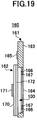
- FIG. 19 is a cross-sectional side view illustrating the plating jig 160 with the semiconductor wafer 100 being mounted therein;
- FIG. 20 is a schematic view illustrating a plating device and the plating method according to the embodiment of the present invention.
- FIG. 21 is an enlarged perspective view of the semiconductor wafer 100 mounted on a plating jig 160 .
- a plating method of forming rerouting pattern on a semiconductor wafer for example, in a Super Chip-Size Package (Super CSP) semiconductor product.
- Super CSP Super Chip-Size Package
- FIG. 8 is a top view of a semiconductor substrate for explaining a plating method according to an embodiment of the present invention.
- FIG. 9 is a cross-sectional view of the semiconductor substrate in FIG. 8 along the line AA′.
- a conductive layer is formed.
- a conductive layer 110 for example, copper
- a semiconductor wafer 100 for example, a silicon wafer having a diameter of 8 inches (20.32 cm).
- the conductive layer 110 may be formed by sputtering, in which ions are sputtered onto the surface of the semiconductor wafer 100 acting as a target by using glow discharge in an environment of argon gas or other discharging gases.
- an insulating layer formed from polyimide or epoxy may be disposed on the semiconductor wafer 100 , and the conductive layer 110 may be deposited on the insulating layer.
- FIG. 10 is a top view of the semiconductor substrate for explaining the plating method of forming the rerouting patterns continued from FIG. 8 according to the embodiment of the present invention.
- FIG. 11 is a cross-sectional view of the semiconductor substrate in FIG. 10 along the line AA′.
- step two a resist layer is formed. Specifically, as illustrated in FIG. 10 and FIG. 11 , a negative resist layer 120 is formed on the conductive layer 110 .
- the resist layer 120 may be either a negative one or a positive one. In the present embodiment, it is assumed that the resist layer 120 is a negative resist layer.
- the negative resist layer 120 has a characteristic in that the portion of the negative resist layer 120 irradiated by ultraviolet rays becomes insoluble or hardly soluble in a developing solution, and remains on the surface of the conductive layer 110 after being developed.
- the negative resist layer 120 is formed by pasting a dry film resist (DFR) on the conductive layer 110 . In this case, it is easy to form the negative resist layer 120 thicker than 10 ⁇ m. Further, it is also easy to remove the negative resist layer 120 after the plating treatment.
- DFR dry film resist
- a 30 ⁇ m thick dry film resist (DFR) is used as the negative resist layer 120 .
- DFR dry film resist
- FIG. 12 is a top view of the semiconductor substrate for explaining the plating method of forming rerouting patterns continued from FIG. 11 according to the embodiment of the present invention.
- step three the first exposure is carried out.
- a protection film 130 which allows transmission of light for exposure, is applied on the negative resist layer 120 to protect the negative resist layer 120 .
- the protection film 130 is formed by PET (Poly Ethylene Terephthalate).
- ink is printed on the protection film 130 , which is above a power feeding electrode on the conductive layer 110 , to form a light shielding layer 145 .
- a reticle pattern (not illustrated) is disposed at a specified position above the negative resist layer 120 , and a projection lithography stepper (not illustrated) emits ultraviolet rays onto the negative resist layer 120 to expose the negative resist layer 120 .
- each cell 200 indicates an area exposed by the projection lithography stepper at one time (referred to as “unit exposure area” below).
- the projection lithography stepper exposes the cells 200 one by one. As described with reference to FIG. 5 , at the edge of the semiconductor wafer 100 , the cells 200 extend out of the semiconductor wafer 100 , thus, these patterns of the reticle cannot be exposed.
- the negative resist layer 120 is exposed through the reticle, and portions of the negative resist layer 120 irradiated by the ultraviolet rays through the reticle becomes insoluble or hardly soluble in the developing solution. But, portions of the negative resist layer 120 shielded by the reticle are not exposed and remains soluble in the developing solution, namely, portions of the negative resist layer 120 corresponding to positions where the plating pattern 150 is to be formed, and portions of the negative resist layer 120 corresponding to positions of a power feeding electrode 115 for supplying electric power during electro-plating and where the light shielding layer 145 is formed presently remains soluble to the developing solution.
- FIG. 13 is a top view of the semiconductor substrate for explaining the plating method of forming the routing patterns continued from FIG. 12 according to the embodiment of the present invention.
- FIG. 14 is a cross-sectional view of the semiconductor substrate in FIG. 13 along the line AA′.
- step four the second exposure is carried out. Specifically, in the second exposure, light for exposure, such as ultraviolet rays, is irradiated onto the peripheral portion of the negative resist layer 120 . In this process, the second exposure is executed with the light shielding layer 145 being present. In addition, the second exposure is performed with focused light from a laser diode.
- light for exposure such as ultraviolet rays
- the exposed region is indicated by meshes in FIG. 13 , and this region is referred to as “peripheral exposure region 140 ”.
- the peripheral exposure region 140 corresponds to a ring-shaped portion at the edge of the negative resist layer 120 on the semiconductor wafer 100 .
- portions of the negative resist layer 120 irradiated by the ultraviolet rays become insoluble or hardly soluble in the developing solution. That is, by step four, the peripheral portion of the negative resist layer 120 (the peripheral exposure region 140 ) become insoluble or hardly soluble in the developing solution, forming a ring-shaped portion. But the portion of the negative resist layer 120 corresponding to the light shielding layer 145 remains soluble to the developing solution.
- the width of the peripheral exposure region 140 along the radial direction of the semiconductor wafer 100 may be set to be 3 mm to 4 mm.
- step five of the plating method according to the present embodiment is executed to perform developing.
- step five the protection film 130 , which is pasted on the negative resist layer 120 , is removed. Then, the semiconductor wafer 100 is immersed into the developing solution for developing.
- the exposed portions of the negative resist layer 120 in step three (first exposure) and step four (second exposure) are insoluble or hardly soluble in the developing solution, and remain on the conductive layer 110 even after developing. Meanwhile, the un-exposed portions of the negative resist layer 120 in step three and step four are soluble in the developing solution, and are removed in the developing step.
- These unexposed portions include the portions of the negative resist layer 120 corresponding to positions where the plating pattern 150 is to be formed, and the portion of the negative resist layer 120 corresponding to positions of the power feeding electrode 115 .
- FIG. 15 is an enlarged perspective view of the peripheral portion of the semiconductor substrate after step five is finished according to the embodiment of the pre sent invention.
- plural plating patterns 150 are formed in the negative resist layer 120 .
- the peripheral exposure region 140 is formed to have a ring shape at the edge of the negative resist layer 120 .
- the power feeding electrode 115 is formed at specified positions. The power feeding electrode 115 is formed at outer edge of the peripheral exposure region 140 , and has a width less than the width of the peripheral exposure region 140 .
- the peripheral exposure region 140 Because of presence of the peripheral exposure region 140 , even the groove-like plating pattern 150 A at the edge of the semiconductor wafer 100 is not in communication with the outside. That is, the portion, where the communication portion 651 is formed otherwise in the related art, is included in the peripheral exposure region 140 in the present embodiment, and this portion is not developed and is not removed. That is, the peripheral exposure region 140 functions as a dam to prevent the plating pattern 150 A from being in communication with the outside.
- step six of the plating method according to the present embodiment is executed to perform plating.
- the semiconductor wafer 100 having the plating patterns 150 is mounted on a plating jig 160 .
- the plating jig 160 roughly includes a mask jig 161 and a rear lid jig 162 .
- FIG. 16A and FIG. 16B are a plan view and a cross-sectional side view, respectively, of the mask jig 161 in the plating jig 160 used in the plating method according to the embodiment of the present invention.
- the mask jig 161 has mask body 163 , in which an opening 164 is formed at a position slightly lower than the center.
- the mask body 163 is formed from a resin.
- External connection terminals 165 are arranged above the mask body 163 , and a sealing rubber 167 and power feeding terminals 166 are arranged surrounding the opening 164 with the sealing rubber 167 and the power feeding terminals 166 being in ring shapes.
- the external connection terminals 165 and the power feeding terminals 166 are electrically connected.
- the power feeding terminals 166 are arranged on the outer side of the sealing rubber 167 .
- plural screw holes 168 are formed at positions on the outer side of the opening 164 .
- screws (not-illustrated) are screwed into these screw holes 168 .
- FIG. 17A and FIG. 17B are a plan view and a cross-sectional side view, respectively, of a rear lid jig 162 in the plating jig 160 used in the plating method according to an embodiment of the present invention.
- the rear lid jig 162 includes a lid body 170 and fixing frames 171 .
- the lid body 170 is disk-shaped, and the size thereof is set to be larger than the diameter of the semiconductor wafer 100 .
- a rear sealing rubber 172 is arranged on the back side of the body 170 .
- the rear sealing rubber 172 has a sufficiently large area so that it touches the whole rear surface of the semiconductor wafer 100 when mounting the semiconductor wafer 100 in a way described below. Further, penetration holes 173 are formed at ends of plural fixing frames 171 (in the present embodiment, there are two fixing frames 171 ).
- FIG. 19 is a cross-sectional side view illustrating the plating jig 160 with the semiconductor wafer 100 being mounted therein.
- the semiconductor wafer 100 In order to mount the semiconductor wafer 100 on the plating jig 160 , first, the semiconductor wafer 100 should be mounted on the mask jig 161 .
- the surface of the semiconductor wafer 100 with the negative resist layer 120 is arranged to face the sealing rubber 167 .
- the sealing rubber 167 is positioned so that the whole sealing rubber 167 can touch the semiconductor wafer 100
- the power feeding electrodes 115 formed on the semiconductor wafer 100 are positioned so as to be connected with the power feeding terminals 166 .
- not-illustrated screws are used to fix the rear lid jig 162 to face the mask jig 161 on which the semiconductor wafer 100 is mounted.
- the rear sealing rubber 172 on the back side of the body 170 is arranged to touch the whole rear surface of the semiconductor wafer 100 .
- the semiconductor wafer 100 is mounted on the plating jig 160 .
- the plating treatment is executed on the semiconductor wafer 100 .
- FIG. 20 is a schematic view illustrating a plating device and the plating method according to the embodiment of the present invention.
- a plating device 180 for plating the semiconductor wafer 100 includes a plating tank 181 , a power supply, a cathode 184 , and an anode 185 .
- a plating solution 182 includes copper ions, and the anode 185 is made from copper.
- the cathode 184 is connected to the external connection terminals 165 of the plating jig 160 . Hence, the cathode 184 is electrically connected with the conductive layer 110 through the external connection terminals 165 , the power feeding terminals 166 , and the power feeding electrodes 115 (as a part of the conductive layer 110 ). In addition, the conductive layer 110 is exposed at the positions where the plating pattern 150 of the negative resist layer 120 is formed. Hence, copper ions are deposited on the conductive layer 110 which has negative polarity, and the rerouting pattern is formed in the plating pattern 150 .
- FIG. 21 is an enlarged perspective view of the semiconductor wafer 100 mounted on a plating jig 160 .
- FIG. 21 illustrates an enlarged peripheral portion of the semiconductor wafer 100 mounted on a plating jig 160 .
- a sealing rubber 167 of the plating jig is shown in FIG. 21 .
- step four the second exposure step
- the peripheral portion of the negative resist layer 120 is exposed, hence, the peripheral exposure region 140 is formed in a ring shape at the edge of the negative resist layer 120 on the semiconductor wafer 100 .
- the peripheral exposure region 140 functions as a dam, and the outer side of the plating pattern 150 A at the edge of the semiconductor wafer 100 is blocked by the peripheral exposure region 140 , and the inner side 152 of the plating pattern 150 A at the edge of the semiconductor wafer 100 is blocked by the peripheral exposure region 140 ,
- the contacting position of the sealing rubber 167 on the semiconductor wafer is not set on the inner side of the peripheral exposure region 140 .
- the sealing rubber 167 is on the peripheral exposure region 140 , and on the inner side of the power feeding electrodes 115 .
- the plating solution 182 it is possible to prevent the plating solution 182 from eroding the power feeding terminal 166 , which forms the plating jig 160 , in addition, it is also possible to prevent adhesion of the plating solution 182 to the back surface of the semiconductor wafer 100 . Further, even when the negative resist layer 120 is a DFR thicker than 10 ⁇ m, because of the presence of the peripheral exposure region 140 , it is possible to reliably prevent leakage of the plating solution 182 in the plating step.
- the thickness of the negative resist layer 120 is set to be 30 ⁇ m. It is found that even when the thickness of the negative resist layer 120 is from 35 ⁇ m to 40 ⁇ m, it is possible to reliably prevent leakage of the plating solution 182 in the plating step.
- the negative resist layer 120 and the peripheral exposure region 140 are removed.
- the semiconductor wafer 100 is formed to include routing patterns having shapes in correspondence to the shape of the plating pattern 150 .
- the present invention is described while taking formation of the rerouting patterns as an example.
- the present invention is not limited to rerouting patterns; it is applicable to formation of conductive posts, bumps, or the like by electrolytic plating.
Landscapes
- Chemical & Material Sciences (AREA)
- Engineering & Computer Science (AREA)
- Chemical Kinetics & Catalysis (AREA)
- Electrochemistry (AREA)
- Materials Engineering (AREA)
- Metallurgy (AREA)
- Organic Chemistry (AREA)
- Physics & Mathematics (AREA)
- General Physics & Mathematics (AREA)
- Electromagnetism (AREA)
- Electroplating Methods And Accessories (AREA)
- Electrodes Of Semiconductors (AREA)
- Internal Circuitry In Semiconductor Integrated Circuit Devices (AREA)
Abstract
Description
Claims (4)
Applications Claiming Priority (2)
| Application Number | Priority Date | Filing Date | Title |
|---|---|---|---|
| JP2004069421A JP3715637B2 (en) | 2004-03-11 | 2004-03-11 | Plating method |
| JP2004-069421 | 2004-03-11 |
Publications (2)
| Publication Number | Publication Date |
|---|---|
| US20050202346A1 US20050202346A1 (en) | 2005-09-15 |
| US7790359B2 true US7790359B2 (en) | 2010-09-07 |
Family
ID=34918491
Family Applications (1)
| Application Number | Title | Priority Date | Filing Date |
|---|---|---|---|
| US11/072,724 Active 2027-11-16 US7790359B2 (en) | 2004-03-11 | 2005-03-04 | Plating method |
Country Status (5)
| Country | Link |
|---|---|
| US (1) | US7790359B2 (en) |
| JP (1) | JP3715637B2 (en) |
| KR (1) | KR20060043811A (en) |
| CN (1) | CN100533686C (en) |
| TW (1) | TW200536063A (en) |
Families Citing this family (11)
| Publication number | Priority date | Publication date | Assignee | Title |
|---|---|---|---|---|
| JP2007299960A (en) * | 2006-04-28 | 2007-11-15 | Toshiba Corp | Semiconductor device and manufacturing method thereof |
| JP5247998B2 (en) * | 2006-08-11 | 2013-07-24 | 株式会社テラミクロス | Manufacturing method of semiconductor device |
| JP2009266995A (en) * | 2008-04-24 | 2009-11-12 | Casio Comput Co Ltd | Manufacturing method of semiconductor device |
| US20120261254A1 (en) * | 2011-04-15 | 2012-10-18 | Reid Jonathan D | Method and apparatus for filling interconnect structures |
| JP5782398B2 (en) | 2012-03-27 | 2015-09-24 | 株式会社荏原製作所 | Plating method and plating apparatus |
| CN102707566A (en) * | 2012-05-22 | 2012-10-03 | 上海宏力半导体制造有限公司 | Photo-etching method |
| JP6328582B2 (en) * | 2014-03-31 | 2018-05-23 | 株式会社荏原製作所 | Plating apparatus and method for determining electrical resistance of electrical contacts of substrate holder |
| CN105575880B (en) * | 2014-10-09 | 2018-10-23 | 中芯国际集成电路制造(上海)有限公司 | A kind of production method of semiconductor devices |
| CN104538287B (en) * | 2014-11-24 | 2017-08-11 | 通富微电子股份有限公司 | Semiconductor manufacturing electroplate jig photoresistance method for forming area in sealing contact |
| US10014170B2 (en) | 2015-05-14 | 2018-07-03 | Lam Research Corporation | Apparatus and method for electrodeposition of metals with the use of an ionically resistive ionically permeable element having spatially tailored resistivity |
| CN106773537B (en) * | 2016-11-21 | 2018-06-26 | 中国电子科技集团公司第十一研究所 | Surface photolithography and wet etching method of a kind of substrate |
Citations (6)
| Publication number | Priority date | Publication date | Assignee | Title |
|---|---|---|---|---|
| JPH08170198A (en) | 1994-12-15 | 1996-07-02 | Nippondenso Co Ltd | Plating jig for semiconductor wafer |
| JPH11204459A (en) | 1998-01-09 | 1999-07-30 | Ebara Corp | Plating tool for semiconductor wafer |
| JP2001156093A (en) * | 1999-11-26 | 2001-06-08 | Casio Comput Co Ltd | Method for manufacturing semiconductor device |
| JP2003031768A (en) | 2001-07-19 | 2003-01-31 | Nec Corp | Semiconductor device and method of manufacturing the same |
| US6550136B1 (en) * | 1999-03-01 | 2003-04-22 | Sumitomo Metal Mining Co., Ltd | Method of fabricating printed wiring board |
| US20030091940A1 (en) * | 2001-11-09 | 2003-05-15 | Mitsubishi Denki Kabushiki Kaisha | Pattern forming method and method of fabricating device |
-
2004
- 2004-03-11 JP JP2004069421A patent/JP3715637B2/en not_active Expired - Fee Related
-
2005
- 2005-03-04 US US11/072,724 patent/US7790359B2/en active Active
- 2005-03-08 TW TW094106931A patent/TW200536063A/en unknown
- 2005-03-10 KR KR1020050019919A patent/KR20060043811A/en not_active Withdrawn
- 2005-03-11 CN CNB200510054563XA patent/CN100533686C/en not_active Expired - Fee Related
Patent Citations (6)
| Publication number | Priority date | Publication date | Assignee | Title |
|---|---|---|---|---|
| JPH08170198A (en) | 1994-12-15 | 1996-07-02 | Nippondenso Co Ltd | Plating jig for semiconductor wafer |
| JPH11204459A (en) | 1998-01-09 | 1999-07-30 | Ebara Corp | Plating tool for semiconductor wafer |
| US6550136B1 (en) * | 1999-03-01 | 2003-04-22 | Sumitomo Metal Mining Co., Ltd | Method of fabricating printed wiring board |
| JP2001156093A (en) * | 1999-11-26 | 2001-06-08 | Casio Comput Co Ltd | Method for manufacturing semiconductor device |
| JP2003031768A (en) | 2001-07-19 | 2003-01-31 | Nec Corp | Semiconductor device and method of manufacturing the same |
| US20030091940A1 (en) * | 2001-11-09 | 2003-05-15 | Mitsubishi Denki Kabushiki Kaisha | Pattern forming method and method of fabricating device |
Also Published As
| Publication number | Publication date |
|---|---|
| JP3715637B2 (en) | 2005-11-09 |
| US20050202346A1 (en) | 2005-09-15 |
| TW200536063A (en) | 2005-11-01 |
| KR20060043811A (en) | 2006-05-15 |
| CN1667802A (en) | 2005-09-14 |
| CN100533686C (en) | 2009-08-26 |
| JP2005256090A (en) | 2005-09-22 |
Similar Documents
| Publication | Publication Date | Title |
|---|---|---|
| US7790359B2 (en) | Plating method | |
| US5019535A (en) | Die attachment method using nonconductive adhesive for use in high density interconnected assemblies | |
| EP2141511B1 (en) | Radiation detector using gas amplication and method for manufacturing the same | |
| US4689874A (en) | Process for fabricating a thin-film solar battery | |
| JP2009527922A (en) | Method for manufacturing segmented contacts for radiation detectors using direct photolithography | |
| KR20160089515A (en) | Direct current superposition freeze | |
| TW202108826A (en) | Substrate holder and plating device | |
| CN109904212B (en) | Organic light-emitting display panel and manufacturing method thereof | |
| US6140155A (en) | Method of manufacturing semiconductor device using dry photoresist film | |
| CN113347799A (en) | Preparation method of MiniLED board | |
| JP2008502156A (en) | Semiconductor device with reduced contact resistance | |
| US20040253802A1 (en) | Method of plating electrode formation | |
| CN101460017A (en) | Thru-hole electroplating method for printed circuit board | |
| JP5247998B2 (en) | Manufacturing method of semiconductor device | |
| KR100246585B1 (en) | B.g.a semiconductor lead frame and fabrication method of it | |
| US12487520B2 (en) | Multi-layer photoresist systems and methods for manufacturing electrochemical deposition printheads | |
| JPH0226016A (en) | Lithography of circuit pattern | |
| CN121174665A (en) | Manufacturing method of battery piece structure | |
| JP7274353B2 (en) | Substrate plating method | |
| JPH01283825A (en) | positive photoresist | |
| US20060073704A1 (en) | Method of forming bump that may reduce possibility of losing contact pad material | |
| JP4087741B2 (en) | Tape carrier, semiconductor module, and method of manufacturing semiconductor module | |
| CN117604584A (en) | Thick metal layered electroplating structure and method thereof | |
| WO2024099415A1 (en) | Battery cell preparation method and battery cell | |
| CN121174664A (en) | Heterojunction battery piece manufacturing method |
Legal Events
| Date | Code | Title | Description |
|---|---|---|---|
| AS | Assignment |
Owner name: SHINKO ELECTRIC INDUSTRIES CO., LTD., JAPAN Free format text: ASSIGNMENT OF ASSIGNORS INTEREST;ASSIGNOR:YAMANO, TAKAHARU;REEL/FRAME:016362/0641 Effective date: 20050228 |
|
| STCF | Information on status: patent grant |
Free format text: PATENTED CASE |
|
| FEPP | Fee payment procedure |
Free format text: PAYOR NUMBER ASSIGNED (ORIGINAL EVENT CODE: ASPN); ENTITY STATUS OF PATENT OWNER: LARGE ENTITY |
|
| FPAY | Fee payment |
Year of fee payment: 4 |
|
| MAFP | Maintenance fee payment |
Free format text: PAYMENT OF MAINTENANCE FEE, 8TH YEAR, LARGE ENTITY (ORIGINAL EVENT CODE: M1552) Year of fee payment: 8 |
|
| MAFP | Maintenance fee payment |
Free format text: PAYMENT OF MAINTENANCE FEE, 12TH YEAR, LARGE ENTITY (ORIGINAL EVENT CODE: M1553); ENTITY STATUS OF PATENT OWNER: LARGE ENTITY Year of fee payment: 12 |