CN100533686C - Plating method - Google Patents
Plating method Download PDFInfo
- Publication number
- CN100533686C CN100533686C CNB200510054563XA CN200510054563A CN100533686C CN 100533686 C CN100533686 C CN 100533686C CN B200510054563X A CNB200510054563X A CN B200510054563XA CN 200510054563 A CN200510054563 A CN 200510054563A CN 100533686 C CN100533686 C CN 100533686C
- Authority
- CN
- China
- Prior art keywords
- resist layer
- negative resist
- semiconductor chip
- electroplating
- pattern
- Prior art date
- Legal status (The legal status is an assumption and is not a legal conclusion. Google has not performed a legal analysis and makes no representation as to the accuracy of the status listed.)
- Active
Links
Images


Classifications
-
- C—CHEMISTRY; METALLURGY
- C25—ELECTROLYTIC OR ELECTROPHORETIC PROCESSES; APPARATUS THEREFOR
- C25D—PROCESSES FOR THE ELECTROLYTIC OR ELECTROPHORETIC PRODUCTION OF COATINGS; ELECTROFORMING; APPARATUS THEREFOR
- C25D5/00—Electroplating characterised by the process; Pretreatment or after-treatment of workpieces
- C25D5/02—Electroplating of selected surface areas
- C25D5/022—Electroplating of selected surface areas using masking means
-
- C—CHEMISTRY; METALLURGY
- C25—ELECTROLYTIC OR ELECTROPHORETIC PROCESSES; APPARATUS THEREFOR
- C25D—PROCESSES FOR THE ELECTROLYTIC OR ELECTROPHORETIC PRODUCTION OF COATINGS; ELECTROFORMING; APPARATUS THEREFOR
- C25D7/00—Electroplating characterised by the article coated
- C25D7/12—Semiconductors
- C25D7/123—Semiconductors first coated with a seed layer or a conductive layer
-
- G—PHYSICS
- G03—PHOTOGRAPHY; CINEMATOGRAPHY; ANALOGOUS TECHNIQUES USING WAVES OTHER THAN OPTICAL WAVES; ELECTROGRAPHY; HOLOGRAPHY
- G03F—PHOTOMECHANICAL PRODUCTION OF TEXTURED OR PATTERNED SURFACES, e.g. FOR PRINTING, FOR PROCESSING OF SEMICONDUCTOR DEVICES; MATERIALS THEREFOR; ORIGINALS THEREFOR; APPARATUS SPECIALLY ADAPTED THEREFOR
- G03F7/00—Photomechanical, e.g. photolithographic, production of textured or patterned surfaces, e.g. printing surfaces; Materials therefor, e.g. comprising photoresists; Apparatus specially adapted therefor
- G03F7/20—Exposure; Apparatus therefor
- G03F7/2022—Multi-step exposure, e.g. hybrid; backside exposure; blanket exposure, e.g. for image reversal; edge exposure, e.g. for edge bead removal; corrective exposure
- G03F7/203—Multi-step exposure, e.g. hybrid; backside exposure; blanket exposure, e.g. for image reversal; edge exposure, e.g. for edge bead removal; corrective exposure comprising an imagewise exposure to electromagnetic radiation or corpuscular radiation
-
- H—ELECTRICITY
- H01—ELECTRIC ELEMENTS
- H01L—SEMICONDUCTOR DEVICES NOT COVERED BY CLASS H10
- H01L21/00—Processes or apparatus adapted for the manufacture or treatment of semiconductor or solid state devices or of parts thereof
- H01L21/02—Manufacture or treatment of semiconductor devices or of parts thereof
- H01L21/04—Manufacture or treatment of semiconductor devices or of parts thereof the devices having at least one potential-jump barrier or surface barrier, e.g. PN junction, depletion layer or carrier concentration layer
- H01L21/18—Manufacture or treatment of semiconductor devices or of parts thereof the devices having at least one potential-jump barrier or surface barrier, e.g. PN junction, depletion layer or carrier concentration layer the devices having semiconductor bodies comprising elements of Group IV of the Periodic System or AIIIBV compounds with or without impurities, e.g. doping materials
- H01L21/28—Manufacture of electrodes on semiconductor bodies using processes or apparatus not provided for in groups H01L21/20 - H01L21/268
- H01L21/283—Deposition of conductive or insulating materials for electrodes conducting electric current
- H01L21/288—Deposition of conductive or insulating materials for electrodes conducting electric current from a liquid, e.g. electrolytic deposition
-
- H—ELECTRICITY
- H01—ELECTRIC ELEMENTS
- H01L—SEMICONDUCTOR DEVICES NOT COVERED BY CLASS H10
- H01L21/00—Processes or apparatus adapted for the manufacture or treatment of semiconductor or solid state devices or of parts thereof
- H01L21/02—Manufacture or treatment of semiconductor devices or of parts thereof
- H01L21/027—Making masks on semiconductor bodies for further photolithographic processing not provided for in group H01L21/18 or H01L21/34
- H01L21/0271—Making masks on semiconductor bodies for further photolithographic processing not provided for in group H01L21/18 or H01L21/34 comprising organic layers
- H01L21/0272—Making masks on semiconductor bodies for further photolithographic processing not provided for in group H01L21/18 or H01L21/34 comprising organic layers for lift-off processes
-
- H—ELECTRICITY
- H01—ELECTRIC ELEMENTS
- H01L—SEMICONDUCTOR DEVICES NOT COVERED BY CLASS H10
- H01L21/00—Processes or apparatus adapted for the manufacture or treatment of semiconductor or solid state devices or of parts thereof
- H01L21/02—Manufacture or treatment of semiconductor devices or of parts thereof
- H01L21/04—Manufacture or treatment of semiconductor devices or of parts thereof the devices having at least one potential-jump barrier or surface barrier, e.g. PN junction, depletion layer or carrier concentration layer
- H01L21/18—Manufacture or treatment of semiconductor devices or of parts thereof the devices having at least one potential-jump barrier or surface barrier, e.g. PN junction, depletion layer or carrier concentration layer the devices having semiconductor bodies comprising elements of Group IV of the Periodic System or AIIIBV compounds with or without impurities, e.g. doping materials
- H01L21/28—Manufacture of electrodes on semiconductor bodies using processes or apparatus not provided for in groups H01L21/20 - H01L21/268
- H01L21/283—Deposition of conductive or insulating materials for electrodes conducting electric current
- H01L21/288—Deposition of conductive or insulating materials for electrodes conducting electric current from a liquid, e.g. electrolytic deposition
- H01L21/2885—Deposition of conductive or insulating materials for electrodes conducting electric current from a liquid, e.g. electrolytic deposition using an external electrical current, i.e. electro-deposition
-
- H—ELECTRICITY
- H01—ELECTRIC ELEMENTS
- H01L—SEMICONDUCTOR DEVICES NOT COVERED BY CLASS H10
- H01L21/00—Processes or apparatus adapted for the manufacture or treatment of semiconductor or solid state devices or of parts thereof
- H01L21/70—Manufacture or treatment of devices consisting of a plurality of solid state components formed in or on a common substrate or of parts thereof; Manufacture of integrated circuit devices or of parts thereof
- H01L21/71—Manufacture of specific parts of devices defined in group H01L21/70
- H01L21/768—Applying interconnections to be used for carrying current between separate components within a device comprising conductors and dielectrics
- H01L21/76838—Applying interconnections to be used for carrying current between separate components within a device comprising conductors and dielectrics characterised by the formation and the after-treatment of the conductors
- H01L21/76885—By forming conductive members before deposition of protective insulating material, e.g. pillars, studs
Abstract
A method of forming an electrode on a semiconductor wafer by plating is disclosed that is able to reliably prevent leakage of a plating solution during the plating process. The plating method comprises the steps of forming a conductive layer on a semiconductor wafer; forming a negative resist layer on the conductive layer; exposing a center portion of the negative resist layer; exposing a peripheral region of the negative resist layer after the step of exposing the center portion of the negative resist layer; developing the exposed negative resist layer to form a predetermined plating pattern; and performing plating on the plating pattern.
Description
Technical field
The present invention relates to by forming the rewiring method of patterning at the enterprising electroplating of semiconductor chip.
Background technology
In semiconductor product, for example, in superchip-size encapsulation (Super CSP) product, form conductive pole (for example, copper post) or rewiring pattern by surperficial enterprising electroplating at the semiconductor chip that from semiconductor chip, downcuts.In addition, in the process that forms lobed semiconductor product, form conductive pole or rewiring pattern.Before carrying out electroplating processes, on semiconductor chip, form electroplated electrode (power feed layer).
For example, Japanese Laid-Open Patent Application No.2003-031768 (the 5th page Fig. 1) has illustrated this technique background technology.
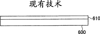
Fig. 1 has shown the process of the formation rewiring pattern in the correlation technique to Fig. 6.
Fig. 1 is the top view of Semiconductor substrate.
Fig. 2 is that Semiconductor substrate among Fig. 1 is along the profile of line AA '.
In step 1, form conductive layer.Specifically, as depicted in figs. 1 and 2, form conductive layer 610 on the semiconductor chip 600 by being injected in.Perhaps, on semiconductor chip 600, can provide the insulating barrier that forms by polyimides or epoxy resin, can depositing conducting layer 610 on insulating barrier.
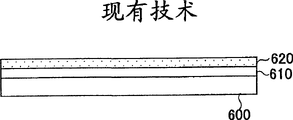
Fig. 3 is used to illustrate the top view of formation from the Semiconductor substrate of the process of the rewiring pattern of Fig. 1 continuation.
Fig. 4 is that Semiconductor substrate among Fig. 3 is along the profile of line AA '.
In step 2, form resist layer.Specifically, as shown in Figure 3 and Figure 4, on conductive layer 610, form negative resist layer 620.Then, after step 2 and before, on resist layer 620, provide the diaphragm (not shown), with protection resist layer 620 in step 3 subsequently (as described below).Here, resist layer 620 can be born, and also can be positive.Below, suppose that resist layer 620 is negative resist layers.
Fig. 5 is used to illustrate the top view of formation from the Semiconductor substrate of the process of the rewiring pattern of Fig. 3 continuation.
In step 3, expose.Specifically, as shown in Figure 5, the assigned address above negative resist layer 620 forms cross line chart (not shown), and projection photoetching steeper (not shown) is sent ultraviolet ray by the cross line chart to negative resist layer 620, so that 620 exposures of negative resist layer.Then, remove the diaphragm of bearing on the resist layer 620.
In grid regions shown in Figure 5, each unit 700 is all represented by the zone of projection photoetching steeper single exposure (below abbreviate " unit exposure " as).Projection photoetching steeper has the cross hairs of the cross line chart (electroplating figure) corresponding to the shape of the electroplated electrode that will form by use, makes unit 700 exposures one by one.
Fig. 6 is used to illustrate the enlarged perspective of formation from the Semiconductor substrate of the process of the rewiring pattern of Fig. 5 continuation.In Fig. 6, after step of exposure as shown in Figure 5, on Semiconductor substrate, develop.
As shown in Figure 6, on semiconductor chip 600, form conductive layer 610, and on conductive layer 610, form resist layer 620 (dotted portion).
Because step of exposure and development step form plated pattern (rewiring pattern) in resist layer 620.In this example, because resist layer 620 is negative resist layers, therefore, it is soluble or solvable hardly in developer solution that the exposed portion of resist layer 620 becomes, and removes unexposed part by development, thereby produce plated pattern 650.In the position that forms plated pattern 650, conductive layer 610 is exposed.
After the semiconductor chip 600 with plated pattern 650 is installed on the electroplating clamp, illustrated as Japanese Laid-Open Patent Application No.8-170198 (Fig. 1 and Fig. 2) and Japanese Laid-Open Patent Application No.11-204459 (Fig. 1), semiconductor chip 600 immersions are filled in the electroplating bath of electroplate liquid, the electroplating (for example, copper facing) of going forward side by side.In this process, caulking gum is provided in electroplating clamp, caulking gum is positioned at the periphery of semiconductor chip 600, so that prevent the liquid infiltration.So, the plating position of an electroplate liquid contact semiconductor sheet 600 can not leak into the back side of semiconductor chip 600.
In above-mentioned electroplating process, in plated pattern 650, plated the conductive metallic material (for example, copper) of appointment; Therefore, in plated pattern 650, form the rewiring pattern.Next, remove negative resist layer 620, on semiconductor chip 600, form rewiring pattern corresponding to plated pattern 650.
Recently, in order to improve the electrical characteristics of rewiring pattern, the someone advises increasing the thickness of the rewiring pattern that forms on semiconductor chip 600.In correlation technique, form resist layer by spraying negativity liquid resist layer in positivity liquid resist layer.Yet, utilize the method, can only form thin resist layer less than 10 μ m, be difficult to increase the thickness of rewiring pattern.Therefore, recently, the someone advises using dry film photoresist (DFR) to increase the thickness of rewiring pattern.
Yet, when used thickness in above-mentioned electroplating process surpasses the dry film resist layer of 10 μ m,, also being difficult to prevent the seepage of electroplate liquid even used caulking gum, electroplate liquid can leak into semiconductor chip 600 and the periphery and the back side.
Fig. 7 is the enlarged perspective of the Semiconductor substrate of installing on electroplating clamp.For convenience of description, the caulking gum 635 that in Fig. 7, has only shown electroplating clamp.In Fig. 7, the interior side contacts of electroplate liquid and caulking gum 635, the position of caulking gum 635 is such, so that electroplate liquid can not leak into the outside of caulking gum 635.
However, as described with reference to figure 5, in step of exposure, the unit 700 of semiconductor chip 600 also is to use cross hairs to expose one by one.In this process, at the edge of semiconductor chip 600, unit 700 extends to semiconductor chip 600 outsides; As a result, these patterns of cross hairs can not be exposed.
Please see Figure the edge of the semiconductor chip 600 in 7, the plated pattern that is similar to groove 650 of the edge of semiconductor chip 600 is communicated with the outside by connected component 651, in other words, and in hole of side surface existence of negativity or positive resist layer 620.Therefore, in plating step, electroplate liquid flows into connected component 651 from the inboard 652 of plated pattern 650, and therefore, although caulking gum 635 is provided, electroplate liquid also can leak into the outside of caulking gum 635.
Simultaneously, for thin negative or positive resist layer 620 (for example, less than 2.0 μ m), when pressing caulking gum 635 on resist layer 620, resist layer 620 bendings are because resist layer 620 is made by barras.In addition, when 635 pairs of resist layers 620 of caulking gum seal, capillarity can take place, when entering plated pattern 650, strain can take place in caulking gum 635.Because electroplate liquid seepage phenomenon when resist layer 620 is relatively thinner, can not take place in these facts.
Summary of the invention
Correspondingly, general objects of the present invention is the one or more problems that solve correlation technique.
More specific purpose of the present invention provides the electro-plating method that can prevent the electroplate liquid seepage reliably.
The invention provides the electro-plating method that comprises the following steps: on semiconductor chip, form conductive layer; On conductive layer, form negative resist layer; Core exposure with negative resist layer; After will bearing the core step of exposing of resist layer, will bear the peripheral region exposure of resist layer; The negative resist layer of exposure is developed to form predetermined plated pattern; And at the enterprising electroplating of plated pattern.
According to the present invention, after the core of negative resist layer is exposed, with the peripheral region exposure of negative resist layer.Therefore, after development step, negative resist layer still is in the peripheral region.As a result, around in the zone, negative resist layer still is not in the peripheral region plated pattern that forms on negative resist layer, as a baffle plate, to prevent electroplate liquid seepage in plating step.
In an embodiment, the thickness of negative resist layer is greater than 10 μ m.
According to the present invention, though the thickness of negative resist layer greater than 10 μ m, and the plated pattern that is obtained is thicker, also can prevent electroplate liquid seepage in plating step.
In an embodiment, negative resist layer is formed by dry film photoresist.
According to the present invention, when negative resist layer is formed by dry film photoresist, can be like a cork on semiconductor chip deposit thickness greater than the negative resist layer of 10 μ m.
In an embodiment, in the step of electroplating, used the sealing electroplating clamp.
According to the present invention,, therefore, can in plating step, prevent the electroplate liquid seepage more effectively owing in the step of electroplating, used the sealing electroplating clamp.
In an embodiment, in will bearing the core step of exposing of resist layer, used projection photoetching steeper, will bear the resist layer exposure with next unit area ground.
By the following detailed description of with reference to the accompanying drawings preferred embodiment being carried out, these targets of the present invention and other targets, characteristics, aspect and advantage will become apparent.
Description of drawings
Fig. 1 is the top view of Semiconductor substrate that shows the process of the formation rewiring pattern in the correlation technique;
Fig. 2 is that Semiconductor substrate among Fig. 1 is along the profile of line AA ';
Fig. 3 is used to illustrate the top view of formation from the Semiconductor substrate of the process of the rewiring pattern of Fig. 1 continuation;
Fig. 4 is that Semiconductor substrate among Fig. 3 is along the profile of line AA ';
Fig. 5 is used to illustrate the top view of formation from the Semiconductor substrate of the process of the rewiring pattern of Fig. 3 continuation;
Fig. 6 is used to illustrate the enlarged perspective of formation from the Semiconductor substrate of the process of the rewiring pattern of Fig. 5 continuation;
Fig. 7 is the enlarged perspective of the Semiconductor substrate of installing on electroplating clamp;
Fig. 8 is used to illustrate the top view of the Semiconductor substrate of electro-plating method according to an embodiment of the invention;
Fig. 9 is that Semiconductor substrate among Fig. 8 is along the profile of line AA ';
Figure 10 is the top view that is used to illustrate the Semiconductor substrate of the electro-plating method that forms the rewiring pattern that continues from Fig. 1 according to an embodiment of the invention;
Figure 11 is that Semiconductor substrate among Fig. 3 is along the profile of line AA ';
Figure 12 is the top view that is used to illustrate the Semiconductor substrate of the electro-plating method that forms the rewiring pattern that continues from Figure 11 according to an embodiment of the invention;
Figure 13 is the top view that is used to illustrate the Semiconductor substrate of the electro-plating method that forms the wiring pattern that continues from Figure 12 according to an embodiment of the invention;
Figure 14 is that Semiconductor substrate among Figure 13 is along the profile of line AA ';
Figure 15 finishes the enlarged perspective of the periphery of Semiconductor substrate afterwards in step 5 according to an embodiment of the invention;
Figure 16 A and Figure 16 B are respectively the plane graph and the side cross-sectional view of the shielding anchor clamps 161 in the electroplating clamp 160 that uses in electro-plating method according to an embodiment of the invention;
Figure 17 A and Figure 17 B are respectively the plane graph and the side cross-sectional view of the bonnet anchor clamps 162 in the electroplating clamp 160 that uses in electro-plating method according to an embodiment of the invention;
Figure 18 is the side cross-sectional view that shows the method for the assembling electroplating clamp 160 that uses in the electro-plating method according to an embodiment of the invention;
Figure 19 is the side cross-sectional view that shows the electroplating clamp 160 that semiconductor chip 100 wherein has been installed;
Figure 20 shows the schematic representation of electroplating device and electro-plating method according to an embodiment of the invention; And
Figure 21 is the enlarged perspective of the semiconductor chip 100 of installation on electroplating clamp 160.
Embodiment
The preferred embodiments of the present invention are described below with reference to the accompanying drawings.
Specifically, putting up with the electro-plating method that forms the rewiring pattern on the big or small semiconductor chip that encapsulates in (super CSP) semiconductor product of superchip is described.
Fig. 8 is used to illustrate the top view of the Semiconductor substrate of electro-plating method according to an embodiment of the invention.
Fig. 9 is that Semiconductor substrate among Fig. 8 is along the profile of line AA '.
In step 1,, form conductive layer as Fig. 8 and shown in Figure 9.Specifically, on semiconductor chip 100, for example, diameter is on the silicon chip of 8 inches (20.32cm), and deposition is used to form the conductive layer 110 (for example, copper) of rewiring pattern.
Can form conductive layer 110 by spraying, in course of injection, in the environment of argon gas or other exhausts,, ion is ejected on the surface of the semiconductor chip 100 that serves as target by using glow discharge.
Perhaps, on semiconductor chip 100, can provide the insulating barrier that forms by polyimides or epoxy resin, can depositing conducting layer 110 on insulating barrier.
Figure 10 is the top view that is used to illustrate the Semiconductor substrate of the electro-plating method that forms the rewiring pattern that continues from Fig. 8 according to an embodiment of the invention.
Figure 11 is that Semiconductor substrate among Figure 10 is along the profile of line AA '.
In step 2, form resist layer.Specifically, as shown in Figure 10 and Figure 11, on conductive layer 110, form negative resist layer 120.
Here, resist layer 120 can be born, and also can be positive.In the present embodiment, suppose that resist layer 120 is negative resist layers.
Negative resist layer 120 has such feature: the part by ultraviolet irradiation of negative resist layer 120 becomes soluble or solvable hardly in developer solution, still can rest on the surface of conductive layer 110 after developing.
Form negative resist layer 120 by on conductive layer 110, pasting dry film photoresist (DFR).In the case, be easy to form the negative resist layer 120 of thickness greater than 10 μ m.In addition, after carrying out electroplating processes, also remove negative resist layer 120 easily.
In the present embodiment, used thickness is the negative resist layer 120 of dry film photoresist (DFR) conduct of 30 μ m.Utilize so thick negative resist layer 120, can form rewiring pattern with low resistance and good electrical characteristics.
Figure 12 is the top view that is used to illustrate the Semiconductor substrate of the electro-plating method that forms the rewiring pattern that continues from Figure 11 according to an embodiment of the invention.
In step 3, as shown in figure 12, carry out the exposure first time.Specifically, at negative resist layer 120 coating protective films 130, to protect negative resist layer 120, this diaphragm allows transmittance, so that expose.For example, form diaphragm 130 with PET (many Polyethyleneglycol Terephthalate).
Next, marking ink on diaphragm 130, this diaphragm 130 is higher than the power feed electrode on the conductive layer 110, to form light shielding layer 145.
Then, assigned address forms cross line chart (not shown) above negative resist layer 120, and projection photoetching steeper (not shown) is sent ultraviolet ray to negative resist layer 120, so that 120 exposures of negative resist layer.
In grid regions shown in Figure 12, each unit 200 is all represented by the zone of projection photoetching steeper single exposure (below abbreviate " unit exposure " as).Projection photoetching steeper exposes to unit 200 one by one.As described with reference to figure 5, at the edge of semiconductor chip 100, unit 200 extends to the outside of semiconductor chip 100, and so, these patterns of cross hairs can not be exposed.
By light shining on the negative resist layer 120 with projection photoetching steeper, negative resist layer 120 is exposed by cross hairs, and the cross hairs that passes through of negative resist layer 120 is become soluble or solvable hardly in developer solution by the part of ultraviolet irradiation.But, the part that is shielded by cross hairs of negative resist layer 120 can not exposed, and still dissolve in developer solution, promptly, those parts of negative resist layer 120 corresponding to the position that will form plated pattern 150, and negative resist layer 120 still dissolve in developer solution corresponding to the position of the power feed electrode 115 that during electroplating, is used to provide power supply and those parts of having formed the position of light shielding layer 145 at present.
Figure 13 is the top view that is used to illustrate the Semiconductor substrate of the electro-plating method that forms the wiring pattern that continues from Figure 12 according to an embodiment of the invention.
Figure 14 is that Semiconductor substrate among Figure 13 is along the profile of line AA '.
In step 4,, carry out the exposure second time as Figure 13 and shown in Figure 14.Specifically, in exposure for the second time, the illumination that is used to expose such as ultraviolet ray is mapped to the periphery of bearing resist layer 120.In this process, when carrying out exposing the second time, there is light shielding layer 145 to exist.In addition, the focused light that utilizes laser diode to send carries out the exposure second time.
In step 4, the zone that is exposed represents that by the grid among Figure 13 this zone is called as " peripheral exposure area 140 ".Peripheral exposure area 140 is corresponding to the annulus of negative resist layer 120 edges on the semiconductor chip 100.
As mentioned above, the part by ultraviolet irradiation of negative resist layer 120 becomes soluble or solvable hardly in developer solution.That is, by step 4, the periphery (peripheral exposure area 140) of negative resist layer 120 becomes soluble or solvable hardly in developer solution, has formed annulus.But the part corresponding to light shielding layer 145 of negative resist layer 120 still dissolves in developer solution.
For example, the width radially along semiconductor chip 100 of peripheral exposure area 140 can be set to 3mm to 4mm.
After step 4 is finished, carry out step 5, to develop according to the electro-plating method of present embodiment.
In step 5, remove the diaphragm 130 that sticks on the negative resist layer 120.Then, semiconductor chip 100 is immersed in the developer solution develops.
As mentioned above, the exposed portion of the negative resist layer 120 in step 3 (exposure for the first time) and the step 4 (exposure for the second time) is soluble or solvable hardly in developer solution, even still is retained on the conductive layer 110 after developing.Simultaneously, the unexposed portion of the negative resist layer 120 in step 3 and the step 4 dissolves in developer solution, and removes in development step.These unexposed parts comprise those parts corresponding to the position that will form plated pattern 150 of negative against corrosion 120, and those parts corresponding to the position of power feed electrode 115 of negative resist layer 120.
Figure 15 finishes the enlarged perspective of the periphery of Semiconductor substrate afterwards in step 5 according to an embodiment of the invention.
As shown in figure 15, by development treatment, a plurality of plated patterns 150 in negative resist layer 120, have been formed.In addition, form peripheral exposure area 140, have the shape of ring with edge at negative resist layer 120.In addition, also form power feed electrode 115 at assigned address.Outward flange in peripheral exposure area 140 forms power feed electrode 115, and its width is less than the width of peripheral exposure area 140.
Because the existence of peripheral exposure area 140, even be positioned at being similar to groove plated pattern 150A and also can not being communicated with of semiconductor chip frontside edge with the outside.That is, otherwise in correlation technique, form the part of connected component 651, comprise that this part can not be developed in the peripheral exposure area 140 in the present embodiment, can and not remove.That is, peripheral exposure area 140 prevents that as a baffle plate plated pattern 150A is communicated with the outside.
After step 5 is finished, carry out step 6, to electroplate according to the electro-plating method of present embodiment.In step 6, at first, the semiconductor chip 100 that will have plated pattern 150 is installed in the electroplating clamp 160.Electroplating clamp 160 roughly comprises shielding anchor clamps 161 and bonnet anchor clamps 162.
Figure 16 A and Figure 16 B are respectively the plane graph and the side cross-sectional view of the shielding anchor clamps 161 in the electroplating clamp 160 that uses in electro-plating method according to an embodiment of the invention.
Shown in Figure 16 A and Figure 16 B, shielding anchor clamps 161 have shield 163, wherein, have formed a hole 164 in the position lower slightly than the center.For example, shield 163 is formed by resin.External connection terminals 165 is provided above shield 163, in the hole 164 around caulking gum 167 and power feed terminal 166 be provided, caulking gum 167 and power feed terminal 166 form annular.
Can switch between external connection terminals 165 and the power feed terminal 166.In addition, power feed terminal 166 is positioned at the outside of caulking gum 167.
In addition, the position in 164 the outside has formed a plurality of screw holes 168 in the hole.After fixing bonnet anchor clamps 162, the bolt (not shown) is screwed in these screw holes 168.
Figure 17 A and Figure 17 B are respectively the plane graph and the side cross-sectional view of the bonnet anchor clamps 162 in the electroplating clamp 160 that uses in electro-plating method according to an embodiment of the invention.
Shown in Figure 17 A and Figure 17 B, bonnet anchor clamps 162 comprise lid body 170 and fixed frame 171.Lid body 170 is discoidal, and its size is set to larger than the diameter of semiconductor chip 100.In addition, provide back caulking gum 172 at the back side of lid body 170.
Back caulking gum 172 has enough big area, so that it can touch the whole back side of semiconductor chip 100 when in the manner as described below semiconductor chip 100 being installed.In addition, the end at a plurality of fixed frames 171 has formed through hole 173 (in the present embodiment, two fixed frames 171 being arranged).
Next, the process of semiconductor chip 100 just being installed with reference to Figure 18 and Figure 19 on electroplating clamp 160 is described.
Figure 18 is the side cross-sectional view that shows the method for the assembling electroplating clamp 160 that uses in the electro-plating method according to an embodiment of the invention.
Figure 19 is the side cross-sectional view that shows the electroplating clamp 160 that semiconductor chip 100 wherein has been installed.
For semiconductor chip 100 is installed on electroplating clamp 160, at first, semiconductor chip 100 should be installed on the shielding anchor clamps 161.
When on shielding anchor clamps 161 semiconductor chip 100 being installed, the surface of semiconductor chip 100 with negative resist layer 120 is towards caulking gum 167.In addition, in this process, the position of caulking gum 167 is such, so that whole caulking gum 167 can touch semiconductor chip 100, the position of the power feed electrode 115 that forms on semiconductor chip 100 is such, so that be connected with power feed terminal 166.
Next, use the bolt that does not show that bonnet anchor clamps 162 are fixing, so that towards the shielding anchor clamps 161 that semiconductor chip 100 has been installed in the above.In this step, the back caulking gum 172 at the back side of lid body 170 contacts with the whole back side of semiconductor chip 100.
So, as shown in figure 19, semiconductor chip 100 is installed on electroplating clamp 160.
When on electroplating clamp as implied above 160, semiconductor chip 100 being installed, on semiconductor chip 100, carry out electroplating processes.
Figure 20 shows the schematic representation of electroplating device and electro-plating method according to an embodiment of the invention.
In Figure 20, the electroplating device 180 that is used for that semiconductor chip 100 is electroplated comprises electroplating bath 181, power supply, negative electrode 184 and anode 185.Here, as example, copper-plated process has been described.Therefore, electroplate liquid 182 comprises copper ion, and anode 185 is formed by copper.
Figure 21 is the enlarged perspective of the semiconductor chip 100 of installation on electroplating clamp 160.
Figure 21 is presented at the amplification periphery of the semiconductor chip of installing on the electroplating clamp 160 100.For convenience of description, the caulking gum 167 that in Figure 21, has only shown electroplating clamp.
In the present embodiment, as mentioned above, in step 4 (step of exposure for the second time), with the periphery exposure of negative resist layer 120, therefore, the edge of the negative resist layer 120 on semiconductor chip 100 forms the peripheral exposure area 140 of annular.Peripheral exposure area 140 is as a baffle plate, and the outside of the plated pattern 150A at semiconductor chip frontside edge place is by 140 blocking-up of peripheral exposure area, and the inboard 152 of the plated pattern 150A at semiconductor chip frontside edge place is by 140 blocking-up of peripheral exposure area.
In addition, the contact position of the caulking gum on the semiconductor chip 167 is not fixed in the inboard of peripheral exposure area 140.Specifically, caulking gum 167 is positioned on the peripheral exposure area 140, is positioned at the inboard of power feed electrode 115.
Because such configuration as shown in figure 21, is immersed in the electroplate liquid 182 even the electroplating clamp 160 of semiconductor chip 100 will be installed, electroplate liquid 182 also can not leak into the outside of caulking gum 167 by plated pattern 150A.
Therefore, can prevent that electroplate liquid 182 corrosion from having constituted the power feed terminal 166 of electroplating clamp 160, in addition, can also prevent that electroplate liquid 182 is attached to the back side of semiconductor chip 100.In addition, even negative resist layer 120 is thickness DFR greater than 10 μ m,, also can prevent electroplate liquid 182 seepage in plating step reliably owing to there is peripheral exposure area 140.
For example, in the present embodiment, the thickness of negative resist layer 120 is set to 30 μ m.Can find, though the thickness of negative resist layer 120 from 35 μ m to 40 μ m, also can prevent electroplate liquid 182 seepage in plating step reliably.
At completing steps 6 (plating) afterwards, remove negative resist layer 120 and peripheral exposure area 140.So, semiconductor chip 100 comprises the wiring pattern that has corresponding to the shape of plated pattern 150.
Be referenced as the specific embodiment that the purpose of illustration selects present invention is described although be, obviously, the present invention is not limited only to these embodiment, and under the situation that does not depart from basic conception of the present invention and scope, those people that are proficient in present technique can carry out many modifications.
For example, hereinbefore, be to adopt the formation of rewiring pattern to come as example that present invention is described.Yet the present invention is not limited only to the rewiring pattern; It also is applicable to the situation that forms conductive pole, projection or the like by metallide.
According to the present invention, can prevent the seepage of electroplate liquid reliably by the plated pattern in the plating step.
Present patent application is based on the Japanese priority patent application No.2004-069421 that proposed on March 11st, 2004, at this full content of having quoted this application as a reference.
Claims (5)
1. an electro-plating method comprises the following steps:
On semiconductor chip, form conductive layer;
On conductive layer, form negative resist layer;
Core exposure with negative resist layer;
After will bearing the core step of exposing of resist layer, will bear the peripheral region exposure of resist layer;
The negative resist layer of exposure is developed to form predetermined plated pattern;
After development step, the plated pattern that forms on negative resist layer is not around in the zone; And
At the enterprising electroplating of plated pattern.
2. method according to claim 1, wherein, the thickness of negative resist layer is greater than 10 μ m.
3. method according to claim 2, wherein, negative resist layer is formed by dry film photoresist.
4. method according to claim 1 wherein, in the step of electroplating, has been used the sealing electroplating clamp.
5. method according to claim 1 wherein, in will bearing the core step of exposing of resist layer, has been used projection photoetching steeper, will bear the resist layer exposure with next unit area ground.
Applications Claiming Priority (2)
| Application Number | Priority Date | Filing Date | Title |
|---|---|---|---|
| JP2004069421A JP3715637B2 (en) | 2004-03-11 | 2004-03-11 | Plating method |
| JP2004069421 | 2004-03-11 |
Publications (2)
| Publication Number | Publication Date |
|---|---|
| CN1667802A CN1667802A (en) | 2005-09-14 |
| CN100533686C true CN100533686C (en) | 2009-08-26 |
Family
ID=34918491
Family Applications (1)
| Application Number | Title | Priority Date | Filing Date |
|---|---|---|---|
| CNB200510054563XA Active CN100533686C (en) | 2004-03-11 | 2005-03-11 | Plating method |
Country Status (5)
| Country | Link |
|---|---|
| US (1) | US7790359B2 (en) |
| JP (1) | JP3715637B2 (en) |
| KR (1) | KR20060043811A (en) |
| CN (1) | CN100533686C (en) |
| TW (1) | TW200536063A (en) |
Families Citing this family (11)
| Publication number | Priority date | Publication date | Assignee | Title |
|---|---|---|---|---|
| JP2007299960A (en) * | 2006-04-28 | 2007-11-15 | Toshiba Corp | Semiconductor device and its manufacturing method |
| JP5247998B2 (en) * | 2006-08-11 | 2013-07-24 | 株式会社テラミクロス | Manufacturing method of semiconductor device |
| JP2009266995A (en) * | 2008-04-24 | 2009-11-12 | Casio Comput Co Ltd | Manufacturing method of semiconductor device |
| US8575028B2 (en) * | 2011-04-15 | 2013-11-05 | Novellus Systems, Inc. | Method and apparatus for filling interconnect structures |
| JP5782398B2 (en) | 2012-03-27 | 2015-09-24 | 株式会社荏原製作所 | Plating method and plating apparatus |
| CN102707566A (en) * | 2012-05-22 | 2012-10-03 | 上海宏力半导体制造有限公司 | Photo-etching method |
| JP6328582B2 (en) * | 2014-03-31 | 2018-05-23 | 株式会社荏原製作所 | Plating apparatus and method for determining electrical resistance of electrical contacts of substrate holder |
| CN105575880B (en) * | 2014-10-09 | 2018-10-23 | 中芯国际集成电路制造(上海)有限公司 | A kind of production method of semiconductor devices |
| CN104538287B (en) * | 2014-11-24 | 2017-08-11 | 通富微电子股份有限公司 | Semiconductor manufacturing electroplate jig photoresistance method for forming area in sealing contact |
| US10014170B2 (en) | 2015-05-14 | 2018-07-03 | Lam Research Corporation | Apparatus and method for electrodeposition of metals with the use of an ionically resistive ionically permeable element having spatially tailored resistivity |
| CN106773537B (en) * | 2016-11-21 | 2018-06-26 | 中国电子科技集团公司第十一研究所 | The photomask surface and wet etching method of a kind of substrate |
Family Cites Families (6)
| Publication number | Priority date | Publication date | Assignee | Title |
|---|---|---|---|---|
| JP3391125B2 (en) | 1994-12-15 | 2003-03-31 | 株式会社デンソー | Plating jig for semiconductor wafer |
| JP4037504B2 (en) | 1998-01-09 | 2008-01-23 | 株式会社荏原製作所 | Semiconductor wafer plating jig |
| JP3415089B2 (en) * | 1999-03-01 | 2003-06-09 | 住友金属鉱山株式会社 | Manufacturing method of printed wiring board |
| JP3430290B2 (en) * | 1999-11-26 | 2003-07-28 | カシオ計算機株式会社 | Method for manufacturing semiconductor device |
| JP4649792B2 (en) | 2001-07-19 | 2011-03-16 | 日本電気株式会社 | Semiconductor device |
| JP2003151875A (en) * | 2001-11-09 | 2003-05-23 | Mitsubishi Electric Corp | Pattern forming method and method of manufacturing device |
-
2004
- 2004-03-11 JP JP2004069421A patent/JP3715637B2/en not_active Expired - Lifetime
-
2005
- 2005-03-04 US US11/072,724 patent/US7790359B2/en active Active
- 2005-03-08 TW TW094106931A patent/TW200536063A/en unknown
- 2005-03-10 KR KR1020050019919A patent/KR20060043811A/en not_active Application Discontinuation
- 2005-03-11 CN CNB200510054563XA patent/CN100533686C/en active Active
Also Published As
| Publication number | Publication date |
|---|---|
| US20050202346A1 (en) | 2005-09-15 |
| KR20060043811A (en) | 2006-05-15 |
| JP2005256090A (en) | 2005-09-22 |
| CN1667802A (en) | 2005-09-14 |
| JP3715637B2 (en) | 2005-11-09 |
| TW200536063A (en) | 2005-11-01 |
| US7790359B2 (en) | 2010-09-07 |
Similar Documents
| Publication | Publication Date | Title |
|---|---|---|
| CN100533686C (en) | Plating method | |
| JP4777644B2 (en) | Semiconductor device and manufacturing method thereof | |
| CN101916722B (en) | Method for preventing metallic coatings at edges of wafers from peeling | |
| CN102446774A (en) | Method of manufacturing a base plate for mounting semiconductor elements | |
| CN1203735C (en) | Method for producing severe tolerance imbedded elements for printing circuit board | |
| CN101201545A (en) | Pholithography and wafer forming by the same | |
| JP5247998B2 (en) | Manufacturing method of semiconductor device | |
| CN103456715B (en) | Intermediary base material and preparation method thereof | |
| CN102548243B (en) | Make the method for circuit board salient point, system and circuit board | |
| CN107666771A (en) | Circuit board structure | |
| CN103140042B (en) | The surface treatment method of printed circuit board (PCB) electroless plating wire | |
| JP2000114412A (en) | Manufacture of circuit board | |
| JP2003023009A (en) | Semiconductor device and method of manufacturing the same | |
| JP2005005453A (en) | Printed wiring board and its manufacturing method | |
| TWI222198B (en) | Fine pitch gold bump fabrication process and its package article | |
| CN112291941B (en) | Printed circuit board and preparation method thereof | |
| TWI700022B (en) | Metal etchback process for circuit board and metal-etchback-treated circuit board | |
| JP4971960B2 (en) | Manufacturing method of semiconductor device | |
| KR20100054394A (en) | Circuit board used for ball grid array package and method for manufacturing the same | |
| JP3816982B2 (en) | Photo via formation method | |
| TW494550B (en) | Manufacture method of annular cathode electrode contact region for tin bump manufacture process | |
| JP2001345538A (en) | Method of manufacturing printed wiring board | |
| JP3785267B2 (en) | Method of forming metal film on insulating material, method of conducting through hole using the same, and method of manufacturing contact probe | |
| TW444259B (en) | Fabricating process of thin ball grid array substrate | |
| JPH1051107A (en) | Manufacture of printed-wiring board, photosensitive composition and dry film photoresist |
Legal Events
| Date | Code | Title | Description |
|---|---|---|---|
| C06 | Publication | ||
| PB01 | Publication | ||
| C10 | Entry into substantive examination | ||
| SE01 | Entry into force of request for substantive examination | ||
| C14 | Grant of patent or utility model | ||
| GR01 | Patent grant |