EP2126978B1 - Agencement de doigts de contact et de plages de soudure de cellule solaire pour une efficacité renforcée - Google Patents
Agencement de doigts de contact et de plages de soudure de cellule solaire pour une efficacité renforcée Download PDFInfo
- Publication number
- EP2126978B1 EP2126978B1 EP08705535.6A EP08705535A EP2126978B1 EP 2126978 B1 EP2126978 B1 EP 2126978B1 EP 08705535 A EP08705535 A EP 08705535A EP 2126978 B1 EP2126978 B1 EP 2126978B1
- Authority
- EP
- European Patent Office
- Prior art keywords
- metal contact
- contact fingers
- solar cell
- solder pad
- negative
- Prior art date
- Legal status (The legal status is an assumption and is not a legal conclusion. Google has not performed a legal analysis and makes no representation as to the accuracy of the status listed.)
- Active
Links
- 229910000679 solder Inorganic materials 0.000 title claims description 70
- 239000002184 metal Substances 0.000 claims description 111
- 238000009792 diffusion process Methods 0.000 claims description 23
- 238000000034 method Methods 0.000 claims description 9
- 230000005855 radiation Effects 0.000 claims description 8
- 210000004027 cell Anatomy 0.000 description 77
- 239000004065 semiconductor Substances 0.000 description 3
- XUIMIQQOPSSXEZ-UHFFFAOYSA-N Silicon Chemical compound [Si] XUIMIQQOPSSXEZ-UHFFFAOYSA-N 0.000 description 1
- 238000005457 optimization Methods 0.000 description 1
- 229910052710 silicon Inorganic materials 0.000 description 1
- 239000010703 silicon Substances 0.000 description 1
- 239000000758 substrate Substances 0.000 description 1
Images


Classifications
-
- H—ELECTRICITY
- H01—ELECTRIC ELEMENTS
- H01L—SEMICONDUCTOR DEVICES NOT COVERED BY CLASS H10
- H01L31/00—Semiconductor devices sensitive to infrared radiation, light, electromagnetic radiation of shorter wavelength or corpuscular radiation and specially adapted either for the conversion of the energy of such radiation into electrical energy or for the control of electrical energy by such radiation; Processes or apparatus specially adapted for the manufacture or treatment thereof or of parts thereof; Details thereof
- H01L31/04—Semiconductor devices sensitive to infrared radiation, light, electromagnetic radiation of shorter wavelength or corpuscular radiation and specially adapted either for the conversion of the energy of such radiation into electrical energy or for the control of electrical energy by such radiation; Processes or apparatus specially adapted for the manufacture or treatment thereof or of parts thereof; Details thereof adapted as photovoltaic [PV] conversion devices
-
- H—ELECTRICITY
- H01—ELECTRIC ELEMENTS
- H01L—SEMICONDUCTOR DEVICES NOT COVERED BY CLASS H10
- H01L31/00—Semiconductor devices sensitive to infrared radiation, light, electromagnetic radiation of shorter wavelength or corpuscular radiation and specially adapted either for the conversion of the energy of such radiation into electrical energy or for the control of electrical energy by such radiation; Processes or apparatus specially adapted for the manufacture or treatment thereof or of parts thereof; Details thereof
- H01L31/02—Details
- H01L31/0224—Electrodes
- H01L31/022408—Electrodes for devices characterised by at least one potential jump barrier or surface barrier
- H01L31/022425—Electrodes for devices characterised by at least one potential jump barrier or surface barrier for solar cells
- H01L31/022441—Electrode arrangements specially adapted for back-contact solar cells
-
- H—ELECTRICITY
- H01—ELECTRIC ELEMENTS
- H01L—SEMICONDUCTOR DEVICES NOT COVERED BY CLASS H10
- H01L31/00—Semiconductor devices sensitive to infrared radiation, light, electromagnetic radiation of shorter wavelength or corpuscular radiation and specially adapted either for the conversion of the energy of such radiation into electrical energy or for the control of electrical energy by such radiation; Processes or apparatus specially adapted for the manufacture or treatment thereof or of parts thereof; Details thereof
- H01L31/02—Details
- H01L31/0224—Electrodes
- H01L31/022408—Electrodes for devices characterised by at least one potential jump barrier or surface barrier
- H01L31/022425—Electrodes for devices characterised by at least one potential jump barrier or surface barrier for solar cells
- H01L31/022433—Particular geometry of the grid contacts
-
- H—ELECTRICITY
- H01—ELECTRIC ELEMENTS
- H01L—SEMICONDUCTOR DEVICES NOT COVERED BY CLASS H10
- H01L31/00—Semiconductor devices sensitive to infrared radiation, light, electromagnetic radiation of shorter wavelength or corpuscular radiation and specially adapted either for the conversion of the energy of such radiation into electrical energy or for the control of electrical energy by such radiation; Processes or apparatus specially adapted for the manufacture or treatment thereof or of parts thereof; Details thereof
- H01L31/02—Details
- H01L31/0224—Electrodes
-
- H—ELECTRICITY
- H01—ELECTRIC ELEMENTS
- H01L—SEMICONDUCTOR DEVICES NOT COVERED BY CLASS H10
- H01L31/00—Semiconductor devices sensitive to infrared radiation, light, electromagnetic radiation of shorter wavelength or corpuscular radiation and specially adapted either for the conversion of the energy of such radiation into electrical energy or for the control of electrical energy by such radiation; Processes or apparatus specially adapted for the manufacture or treatment thereof or of parts thereof; Details thereof
- H01L31/04—Semiconductor devices sensitive to infrared radiation, light, electromagnetic radiation of shorter wavelength or corpuscular radiation and specially adapted either for the conversion of the energy of such radiation into electrical energy or for the control of electrical energy by such radiation; Processes or apparatus specially adapted for the manufacture or treatment thereof or of parts thereof; Details thereof adapted as photovoltaic [PV] conversion devices
- H01L31/042—PV modules or arrays of single PV cells
-
- H—ELECTRICITY
- H01—ELECTRIC ELEMENTS
- H01L—SEMICONDUCTOR DEVICES NOT COVERED BY CLASS H10
- H01L31/00—Semiconductor devices sensitive to infrared radiation, light, electromagnetic radiation of shorter wavelength or corpuscular radiation and specially adapted either for the conversion of the energy of such radiation into electrical energy or for the control of electrical energy by such radiation; Processes or apparatus specially adapted for the manufacture or treatment thereof or of parts thereof; Details thereof
- H01L31/18—Processes or apparatus specially adapted for the manufacture or treatment of these devices or of parts thereof
-
- Y—GENERAL TAGGING OF NEW TECHNOLOGICAL DEVELOPMENTS; GENERAL TAGGING OF CROSS-SECTIONAL TECHNOLOGIES SPANNING OVER SEVERAL SECTIONS OF THE IPC; TECHNICAL SUBJECTS COVERED BY FORMER USPC CROSS-REFERENCE ART COLLECTIONS [XRACs] AND DIGESTS
- Y02—TECHNOLOGIES OR APPLICATIONS FOR MITIGATION OR ADAPTATION AGAINST CLIMATE CHANGE
- Y02E—REDUCTION OF GREENHOUSE GAS [GHG] EMISSIONS, RELATED TO ENERGY GENERATION, TRANSMISSION OR DISTRIBUTION
- Y02E10/00—Energy generation through renewable energy sources
- Y02E10/50—Photovoltaic [PV] energy
Definitions
- the present invention relates generally to solar cells and more particularly but not exclusively to solar cell interconnect structures.
- WO 02/23639 A1 relates to a photovoltaic component with a doped wafer, a light-receiving side, an electric bonding side and a semiconductor structure.
- Solar cells are well known devices for converting solar radiation to electrical energy. They may be fabricated on a semiconductor wafer using semiconductor processing technology. Generally speaking, a solar cell may be fabricated by forming P-type and N-type diffusion regions in a silicon substrate. Solar radiation impinging on the solar cell creates electrons and holes that migrate to the diffusion regions, thereby creating voltage differentials between the diffusion regions. In a backside junction solar cell, both the diffusion regions and the metal contact fingers coupled to them are on the backside of the solar cell. The contact fingers allow an external electrical circuit to be coupled to and be powered by the solar cell.
- Efficiency is an important characteristic of a solar cell as it is directly related to the solar cell's capability to generate power. Accordingly, techniques for increasing the efficiency of solar cells are generally desirable.
- the present invention provides improved solar cell contact fingers and solder pad arrangements that allow for higher efficiency compared to conventional solar cells.
- a method of arranging contact structures on a solar cell is defined in claim 1.
- a solar cell is defined in claim 6.
- a solar cell in one embodiment, includes negative metal contact fingers electrically connected to N-type diffusion regions of the solar cell and positive metal contact fingers electrically connected to P-type diffusion regions of the solar cell. Both the N-type and P-type diffusion regions are on the backside of the solar cell.
- the solar cell includes a front side that faces the sun during normal operation.
- the negative and positive metal contact fingers may be interdigitated.
- the metal contact fingers may be arranged to point to and collectively cover portions of a perimeter of a solder pad.
- the negative metal contact fingers may be arranged to point to and collectively cover two or three sides of a solder pad.
- FIG. 1 shows a backside of an example conventional solar cell 100.
- the solar cell 100 includes a plurality of solder pads 102 (i.e., 102-1, 102-2,...) and bus bars 101 (i.e., 101-1, 101-2,...) on each edge portion.
- the solder pads 102 and bus bars 101 have been generally marked with dashed lines.
- the solder pads 102-1, 102-2, and 102-3 are on the negative polarity edge portion of the solar cell 100, while the solder pads 102-4, 102-5, and 102-6 are on the positive polarity edge portion.
- the solder pads 102 provide a surface on which an interconnect lead electrically connecting the solar cell 102 to another solar cell may be attached.
- the bus bars 101 electrically connect metal contact fingers of a particular polarity to their closest corresponding solder pad 102 on a particular edge portion.
- FIG. 2 shows a magnified view of the lower left side of the solar cell 100 of FIG. 1 .
- FIG. 2 also labels the metal contact fingers 201 and 202.
- Metal contact fingers 201 electrically connect the P-type diffusion regions of the solar cell 100 to the solder pads 102 and bus bars 101 on the positive edge portion.
- Metal contact fingers 202 electrically connect the N-type diffusion regions of the solar cell 100 to the solder pads 102 and bus bars 101 on the negative edge portion. Only one metal contact finger 201 and metal contact finger 202 has been labeled to avoid cluttering the figure.
- the metal contact fingers 201 and 202 are arranged such that they point towards the edge portion of the solar cell 100.
- the bus bar 101 is arranged to occupy an increasingly larger area, hence the tapered bus bars 101 of the solar cell 100. This design feature is further explained with reference to FIG. 3 .
- FIG. 3 schematically shows metal contact fingers 303 and 304 having ends that are oriented toward an edge portion 306.
- the metal contact fingers 303 electrically connect to a bus bar 301, which in turn terminates to a solder pad (not shown).
- the metal contact fingers 304 electrically connect to a solder pad on the other edge portion (not shown) of the solar cell.
- Each metal contact finger 303 has a width "W".
- the bus bar 301 is tapered to have an increasing width as measured from the edge portion 306. In FIG. 3 , the bus bar 301 widens left to right from a width of W to 4 W (i.e., four times the width W ).
- the inventor discovered that there is very little solar radiation collection on regions of the solar cell 100 occupied by the bus bars 101.
- the inventor also discovered that efficiency of a solar cell can be enhanced by interdigitating metal contact fingers on areas previously occupied by bus bars. One way of doing so is to orient the metal contact fingers such that their ends point to and collectively cover substantial portions of a perimeter of a solder pad. Embodiments of the present invention are now described beginning with FIG. 4 .
- FIG. 4 schematically shows a solar cell contact arrangement in accordance with an embodiment of the present invention.
- metal contact fingers 413 and 414 are interdigitated, with the metal contact fingers 413 being electrically connected to N-type diffusion regions on the backside of the solar cell and the metal contact fingers 414 being electrically connected to P-type diffusion regions also on the backside of the solar cell.
- the metal contact fingers 414 electrically connect to solder pads (not shown) on the other side of the solar cell opposite to an edge 416.
- Each metal contact finger 413 has a width "W" in the example of FIG. 4 . Ends of some of the metal contact fingers 413 have been generally bounded by dashed lines 418 for ease of illustration.
- the metal contact fingers 413 may be arranged to have their ends point towards the solder pad 410. More particularly, in the example of FIG. 4 , the metal contact fingers 413 end on a perimeter 417 of the solder pad 410. This removes the bus bar that predominantly has a single polarity contact, with one that is interdigitated with positive and negative contacts. Put another way, the conventional bus bar has been eliminated to reclaim more of the solar cell surface for solar radiation collection.
- the metal contact fingers 413 are arranged to have their ends surround three sides of a rectangular solder pad 410, which is equivalent to surrounding about 75% of the perimeter 417 in FIG. 4 .
- the ends of the metal contact fingers 413 are arranged such that they point towards and surround as much of the perimeter of 417 as possible or at least 50% of the solder pad 410.
- the solder pad 410 does not necessarily have to be rectangular.
- the ends of the metal contact fingers 413 may be configured to point to and surround the perimeter of the solder pad within a 180° radius, 90° radius, etc.
- Each metal contact finger 413 preferably terminates on the perimeter of the solar pad 410. However, for optimization purposes, two metal contact fingers may end on the same contact finger, which in turn ends directly on the solder pad 410.
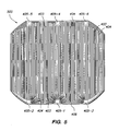
- FIG. 5 shows a backside view of a solar cell 500 in accordance with an embodiment of the present invention.
- the solar cell 500 includes a plurality of solder pads 405 (i.e., 405-1, 405-2,...) on opposing edges of the solar cell.
- the solder pads 405 have been generally marked with dashed lines.
- the solder pads 405-1, 405-2, and 405-3 are on the negative edge portion of the solar cell 500, while the solder pads 405-4, 405-5, and 405-6 are on the positive edge portion.
- the solder pads 405 provide a surface on which an interconnect lead electrically connecting the solar cell 500 to another solar cell may be attached.
- Metal contact fingers 404 electrically connect the P-type diffusion regions of the solar cell 500 to the solder pads 405 on the positive edge portion.
- Metal contact fingers 403 electrically connect the N-type diffusion regions of the solar cell 500 to the solder pads 405 on the negative edge portion.
- a solder pad 405 may only connect to a metal contact finger for the same polarity. Only a few of the metal contact fingers 403 and 404 have been labeled in the interest of clarity.
- FIG. 6 shows a magnified view of the negative edge portion of the solar cell 500, which is at the bottom of FIG. 5 .
- the metal contact fingers 403 and 404 and solder pads 405 are laid out using the principles previously described with reference to FIG. 4 .
- the metal contact fingers 403 are arranged such that their ends are oriented to point towards and surround the perimeter of the solder pad 405, covering 75% (three sides) for the solder pad 405-1 and 50% (two sides) for the solder pads 405-2 and 405-3. Note that what was previously occupied by bus bars 101-1 and 101-2 in the solar cell 100 of FIG. 1 has now been occupied by interdigitated metal contact fingers 403 and 404, with the metal contact fingers leading to the solder pad 405-1.
- some pairs of metal contact fingers 403 join or branch in together to share a contact finger that electrically connects to and terminates on a solder pad 405.
- Preferably three or less metal contact fingers may join together to a single metal contact finger that leads towards and terminates on a solder pad 405. Joining more than three metal contact fingers would result in the shared metal contact finger having a width greater than three times the width of a single metal contact finger. This may result in unacceptable efficiency penalty, depending on the width of each metal contact finger.
- FIG. 7 shows a magnified view of the positive edge portion of the solar cell 500, which is at the top of FIG. 5 . Similar to metal contact fingers 403, some metal contact fingers 404 join together at a single metal contact finger that electrically connects to and terminates on a solder pad 405. In the example of FIG. 7 , because the areas occupied by the P-type metal contacts and diffusion regions are generally more than the N-type metal contacts and diffusion regions, three metal contact fingers 404 may share the same metal contact finger that terminates on the solder pad 405.
- the metal contact fingers 404 bend at about 90° angle to lead into corresponding solder pad 405 (e.g., 405-4), while the metal contact fingers 403 bend at an angle greater than 90° to lead into corresponding solder pad 405 (e.g., solder pad 405-1).
- the metal contact fingers 404 may thus be thought of as having a right angle bend, whereas the metal contact fingers 403 may be thought of as being formed like spokes of a wheel.
- either the positive (i.e., metal contact fingers 404) or the negative (i.e., metal contact fingers 403) metal contact fingers may have the right angle or spoke configuration, and both positive and negative metal contact fingers may have the same configuration.
- two or three metal contact fingers may branch out from a single metal contact finger that leads towards and directly terminates on a corresponding solder pad.
- FIG. 8 shows a cross-section view of the solar cell 500 in accordance with an embodiment of the present invention.
- the solar cell 500 is a backside junction solar cell in that its N-type diffusion regions 703 and P-type diffusion regions 704 are on the backside 706 of the solar cell.
- the front side 707 of the solar cell 500 faces the sun to collect solar radiation.
- the metal contact fingers 403 electrically connect to the N-type diffusion regions 703 and the metal contact fingers 404 (only one is shown for clarity of illustration) electrically connect to the P-type diffusion regions 704 on the backside 706.
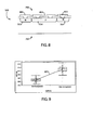
- FIG. 9 shows plots illustrating the efficiency of solar cells with the metal contact fingers and solder pads arranged as per the solar cell 500 (labeled as "new arrangement") compared to a solar cell with metal contact fingers and solder pads arranged as per the solar cell 100 (labeled as "old arrangement”).
- the vertical axis represents efficiency and the horizontal axis indicates plots for the new and old arrangements.
- a line 803 points to the average efficiencies of the solar cells 100 and 500.
- the average efficiency of the solar cells 500 is higher than that of the solar cells 100. In the study, it has been found that the average efficiency of the solar cells 500 is about 21.2%, whereas the average efficiency of the solar cells 100 is about 20.6%.
Claims (12)
- Procédé d'agencement de structures de contact sur une pile solaire, le procédé comprenant :l'entrelacement d'une pluralité de doigts de contact métalliques négatifs (403, 413) avec une pluralité de doigts de contact métalliques positifs (404, 414), les doigts de contact métalliques négatifs (403, 413) étant connectés électriquement à des régions de diffusion de type N sur une face arrière d'une pile solaire, les doigts de contact métalliques positifs (404, 414) étant connectés électriquement à des régions de diffusion de type P sur la face arrière de la pile solaire, la pile solaire incluant une face avant qui fait face au soleil pendant le fonctionnement normal ; etcaractérisé parla mise en place des doigts de contact métalliques négatifs (403, 413) de façon à avoir leurs extrémités pointant en direction de, et entourant collectivement, au moins 50 % d'un périmètre (417) d'au moins une première pastille de soudure (405-1, 405-2, 405-3, 410), la première pastille de soudure (405-1, 405-2, 405-3, 410) étant connectée électriquement aux doigts de contact métalliques négatifs (403, 413), mais pas aux doigts de contact métalliques positifs (404, 414) ; etla mise en place des doigts de contact métalliques positifs (404, 414) de façon à avoir leurs extrémités pointant en direction de, et couvrant collectivement, au moins 50 % d'un périmètre d'une deuxième pastille de soudure (405-4, 405-5, 405-6), la deuxième pastille de soudure (405-4, 405-5, 405-6) étant connectée électriquement aux doigts de contact métalliques positifs (404, 414), mais pas aux doigts de contact métalliques négatifs (403, 413).
- Procédé selon la revendication 1, dans lequel il n'y a aucun doigt de contact métalliques dont une largeur est supérieure à deux fois celle d'un des doigts de contact métalliques négatifs (403, 413) et qui mène à, et se termine sur, la première pastille de soudure.
- Procédé selon la revendication 1 ou 2, dans lequel les doigts de contact métalliques négatifs (403, 413) se terminent sur la première pastille de soudure (405-1, 405-2, 405-3, 410).
- Procédé selon l'une quelconque des revendications 1 à 3, dans lequel les doigts de contact métalliques négatifs (403, 413) pointent en direction de, et entourent collectivement, trois côtés du périmètre de la première pastille de soudure (405-1, 405-2, 405-3, 410).
- Procédé selon l'une quelconque des revendications 1 à 4, dans lequel les doigts de contact métalliques négatifs (403, 413) pointent en direction de, et entourent collectivement, 75 % du périmètre de la première pastille de soudure (405-1, 405-2, 405-3, 410).
- Pile solaire comprenant :une pluralité de doigts de contact métalliques positifs (404, 414), chacun des doigts de contact métalliques positifs (404, 414) étant couplé à une ou plusieurs régions de diffusion de type P sur une face arrière de la pile solaire, une face avant de la pile solaire faisant face au soleil pendant le fonctionnement normal pour collecter le rayonnement solaire ;une pluralité de doigts de contact métalliques négatifs (403, 413), chacun des doigts de contact métalliques négatifs (403, 413) étant couplé à une ou plusieurs régions de diffusion de type N sur la face arrière de la pile solaire, les doigts de contact métalliques négatifs (403, 413) étant entrelacés avec les doigts de contact métalliques positifs (404, 414) ; etcaractérisé parau moins une première pastille de soudure (405-1, 405-2, 405-3, 410) connectée électriquement aux doigts de contact métalliques négatifs (403, 413), mais pas aux doigts de contact métalliques positifs (404, 414), les doigts de contact métalliques négatifs (403, 413) possédant des extrémités pointant vers, et entourant collectivement, au moins 50 % d'un périmètre (417) de la première pastille de soudure (405-1, 405-2, 405-3, 410) ; etune deuxième pastille de soudure (405-4, 405-5, 405-6) connectée électriquement aux doigts de contact métalliques positifs, mais pas aux doigts de contact métalliques négatifs sur une partie de bord de la pile solaire opposée à l'endroit où se trouve la première pastille de soudure (405-1, 405-2, 405-3, 410).
- Pile solaire selon la revendication 6, dans laquelle il n'y a aucun doigt de contact métallique possédant une largeur supérieure à deux fois celle d'un des doigts de contact métalliques négatifs menant à, et se terminant sur, la première pastille de soudure (405-1, 405-2, 405-3, 410).
- Pile solaire selon la revendication 6 ou 7, dans laquelle les doigts de contact métalliques négatifs (403, 413) se terminent sur la première pastille de soudure (405-1, 405-2, 405-3, 410).
- Pile solaire selon l'une quelconque des revendications 6 à 8, dans laquelle au moins deux des doigts de contact métalliques négatifs (403, 413) partagent un autre doigt de contact métallique qui pointe vers, et se termine sur, la première pastille de soudure (405-1, 405-2, 405-3, 410).
- Pile solaire selon l'une quelconque des revendications 6 à 9, dans laquelle les doigts de contact métalliques négatifs (403, 413) sont disposés pour se plier en direction de la première pastille de soudure (405-1, 405-2, 405-3, 410) au moins sur des extrémités opposées de la première pastille de soudure (405-1, 405-2, 405-3, 410).
- Pile solaire selon l'une quelconque des revendications 6 à 10, dans laquelle les doigts de contact métalliques positifs (404, 414) sont disposés pour se plier en direction de la deuxième pastille de soudure (405-4, 405-5, 405-6).
- Pile solaire selon la revendication 11, dans laquelle les doigts de contact métalliques positifs (404, 414) se plient selon un angle de 90°.
Priority Applications (1)
| Application Number | Priority Date | Filing Date | Title |
|---|---|---|---|
| EP16179295.7A EP3096354B1 (fr) | 2007-03-16 | 2008-01-09 | Doigts de contact de cellule solaire et agencement de plage d'accueil pour une efficacité améliorée |
Applications Claiming Priority (2)
| Application Number | Priority Date | Filing Date | Title |
|---|---|---|---|
| US11/725,023 US7804022B2 (en) | 2007-03-16 | 2007-03-16 | Solar cell contact fingers and solder pad arrangement for enhanced efficiency |
| PCT/US2008/000335 WO2008115309A2 (fr) | 2007-03-16 | 2008-01-09 | Agencement de doigts de contact et de plages de soudure de cellule solaire pour une efficacité renforcée |
Related Child Applications (2)
| Application Number | Title | Priority Date | Filing Date |
|---|---|---|---|
| EP16179295.7A Division-Into EP3096354B1 (fr) | 2007-03-16 | 2008-01-09 | Doigts de contact de cellule solaire et agencement de plage d'accueil pour une efficacité améliorée |
| EP16179295.7A Division EP3096354B1 (fr) | 2007-03-16 | 2008-01-09 | Doigts de contact de cellule solaire et agencement de plage d'accueil pour une efficacité améliorée |
Publications (3)
| Publication Number | Publication Date |
|---|---|
| EP2126978A2 EP2126978A2 (fr) | 2009-12-02 |
| EP2126978A4 EP2126978A4 (fr) | 2014-08-20 |
| EP2126978B1 true EP2126978B1 (fr) | 2016-08-24 |
Family
ID=39761438
Family Applications (2)
| Application Number | Title | Priority Date | Filing Date |
|---|---|---|---|
| EP08705535.6A Active EP2126978B1 (fr) | 2007-03-16 | 2008-01-09 | Agencement de doigts de contact et de plages de soudure de cellule solaire pour une efficacité renforcée |
| EP16179295.7A Active EP3096354B1 (fr) | 2007-03-16 | 2008-01-09 | Doigts de contact de cellule solaire et agencement de plage d'accueil pour une efficacité améliorée |
Family Applications After (1)
| Application Number | Title | Priority Date | Filing Date |
|---|---|---|---|
| EP16179295.7A Active EP3096354B1 (fr) | 2007-03-16 | 2008-01-09 | Doigts de contact de cellule solaire et agencement de plage d'accueil pour une efficacité améliorée |
Country Status (7)
| Country | Link |
|---|---|
| US (1) | US7804022B2 (fr) |
| EP (2) | EP2126978B1 (fr) |
| JP (2) | JP5317209B2 (fr) |
| KR (1) | KR101462699B1 (fr) |
| CN (4) | CN101689554A (fr) |
| AU (1) | AU2008227171B2 (fr) |
| WO (1) | WO2008115309A2 (fr) |
Families Citing this family (38)
| Publication number | Priority date | Publication date | Assignee | Title |
|---|---|---|---|---|
| JP5687837B2 (ja) * | 2007-02-16 | 2015-03-25 | ナノグラム・コーポレイションNanoGram Corporation | 太陽電池構造体、光起電モジュール及びこれらに対応する方法 |
| DE102008043750A1 (de) * | 2008-11-14 | 2010-05-20 | Q-Cells Se | Verfahren zur Makierung/Codierung einer Solarzelle und Solarzelle |
| US20100294349A1 (en) * | 2009-05-20 | 2010-11-25 | Uma Srinivasan | Back contact solar cells with effective and efficient designs and corresponding patterning processes |
| US20120211050A1 (en) * | 2009-12-25 | 2012-08-23 | Mitsubishi Electric Corporation | Solar battery module |
| KR101109087B1 (ko) * | 2009-12-31 | 2012-01-31 | 주식회사 효성 | 효율 개선된 태양전지 및 그의 연결방법 |
| US8383235B2 (en) * | 2010-02-04 | 2013-02-26 | The Procter & Gamble Company | Fibrous structures |
| US8912083B2 (en) | 2011-01-31 | 2014-12-16 | Nanogram Corporation | Silicon substrates with doped surface contacts formed from doped silicon inks and corresponding processes |
| CN103503157A (zh) * | 2011-04-26 | 2014-01-08 | 松下电器产业株式会社 | 太阳能电池单元、接合结构体、及太阳能电池单元的制造方法 |
| WO2013031297A1 (fr) * | 2011-08-31 | 2013-03-07 | 三洋電機株式会社 | Procédé de fabrication de module de piles solaires |
| EP2568063A1 (fr) | 2011-09-09 | 2013-03-13 | Rohm and Haas Electronic Materials LLC | Procédé d'électrodéposition de cuivre à faible contrainte interne |
| JP6048837B2 (ja) * | 2011-09-15 | 2016-12-21 | パナソニックIpマネジメント株式会社 | 太陽電池モジュール |
| US9553225B2 (en) | 2012-04-11 | 2017-01-24 | Schneider Electric USA, Inc. | Tapered trunking system with distributed combiner |
| US9306085B2 (en) * | 2012-08-22 | 2016-04-05 | Sunpower Corporation | Radially arranged metal contact fingers for solar cells |
| US8936709B2 (en) | 2013-03-13 | 2015-01-20 | Gtat Corporation | Adaptable free-standing metallic article for semiconductors |
| JP6141223B2 (ja) | 2013-06-14 | 2017-06-07 | 三菱電機株式会社 | 受光素子モジュールおよびその製造方法 |
| US9437756B2 (en) * | 2013-09-27 | 2016-09-06 | Sunpower Corporation | Metallization of solar cells using metal foils |
| US9865757B2 (en) | 2014-04-23 | 2018-01-09 | Helion Concepts, Inc. | Method for quick self interconnection of photovoltaic cell arrays and panels |
| US10249775B2 (en) | 2014-06-11 | 2019-04-02 | Shin-Etsu Chemical Co., Ltd. | Solar cell and method for producing solar cell |
| GB2530583A (en) * | 2014-09-29 | 2016-03-30 | Rec Solar Pte Ltd | Solar cell with specific front surface electrode design |
| JP6199839B2 (ja) | 2014-09-30 | 2017-09-20 | 信越化学工業株式会社 | 太陽電池及びその製造方法 |
| KR101772542B1 (ko) | 2015-04-30 | 2017-08-29 | 엘지전자 주식회사 | 태양 전지 및 이를 포함하는 태양 전지 패널 |
| US10535790B2 (en) | 2015-06-25 | 2020-01-14 | Sunpower Corporation | One-dimensional metallization for solar cells |
| US10573763B2 (en) * | 2015-12-29 | 2020-02-25 | Sunpower Corporation | Solar cell having a plurality of sub-cells coupled by a metallization structure having a metal bridge |
| US11025193B2 (en) | 2016-08-16 | 2021-06-01 | Helion Concepts, Inc. | Compact, low-profile, multiply configurable solar photovoltaic module with concealed connectors |
| USD822890S1 (en) | 2016-09-07 | 2018-07-10 | Felxtronics Ap, Llc | Lighting apparatus |
| US20180309003A1 (en) | 2017-04-24 | 2018-10-25 | Helion Concepts, Inc. | Lightweight solar panels with solar cell structural protection |
| US10775030B2 (en) | 2017-05-05 | 2020-09-15 | Flex Ltd. | Light fixture device including rotatable light modules |
| USD872319S1 (en) | 2017-08-09 | 2020-01-07 | Flex Ltd. | Lighting module LED light board |
| USD862777S1 (en) | 2017-08-09 | 2019-10-08 | Flex Ltd. | Lighting module wide distribution lens |
| USD832494S1 (en) | 2017-08-09 | 2018-10-30 | Flex Ltd. | Lighting module heatsink |
| USD833061S1 (en) | 2017-08-09 | 2018-11-06 | Flex Ltd. | Lighting module locking endcap |
| USD846793S1 (en) | 2017-08-09 | 2019-04-23 | Flex Ltd. | Lighting module locking mechanism |
| USD877964S1 (en) | 2017-08-09 | 2020-03-10 | Flex Ltd. | Lighting module |
| USD832495S1 (en) | 2017-08-18 | 2018-10-30 | Flex Ltd. | Lighting module locking mechanism |
| USD862778S1 (en) | 2017-08-22 | 2019-10-08 | Flex Ltd | Lighting module lens |
| USD888323S1 (en) | 2017-09-07 | 2020-06-23 | Flex Ltd | Lighting module wire guard |
| KR102393953B1 (ko) | 2017-12-07 | 2022-05-03 | 현대에너지솔루션(주) | 에지 수집전극을 구비하는 태양전지 및 이를 포함하는 태양전지 모듈 |
| US20200105951A1 (en) * | 2018-09-28 | 2020-04-02 | Sunpower Corporation | Solar cell with wraparound finger |
Family Cites Families (24)
| Publication number | Priority date | Publication date | Assignee | Title |
|---|---|---|---|---|
| JPS5563884A (en) * | 1978-11-08 | 1980-05-14 | Agency Of Ind Science & Technol | Light-condensation solar battery |
| JPS577976A (en) * | 1980-06-17 | 1982-01-16 | Matsushita Electric Ind Co Ltd | Photo electromotive force element |
| JPS6141266Y2 (fr) * | 1981-04-30 | 1986-11-25 | ||
| US4478879A (en) * | 1983-02-10 | 1984-10-23 | The United States Of America As Represented By The Administrator Of The National Aeronautics And Space Administration | Screen printed interdigitated back contact solar cell |
| JPS59172779A (ja) * | 1983-03-23 | 1984-09-29 | Toshiba Corp | 太陽電池 |
| US4933022A (en) * | 1988-11-14 | 1990-06-12 | Board Of Trustees Of The Leland Stanford Univ. & Electric Power Research Institute | Solar cell having interdigitated contacts and internal bypass diodes |
| US4927770A (en) | 1988-11-14 | 1990-05-22 | Electric Power Research Inst. Corp. Of District Of Columbia | Method of fabricating back surface point contact solar cells |
| US5053083A (en) | 1989-05-08 | 1991-10-01 | The Board Of Trustees Of The Leland Stanford Junior University | Bilevel contact solar cells |
| DE19525720C2 (de) * | 1995-07-14 | 1998-06-10 | Siemens Solar Gmbh | Herstellungsverfahren für eine Solarzelle ohne Vorderseitenmetallisierung |
| US5641362A (en) * | 1995-11-22 | 1997-06-24 | Ebara Solar, Inc. | Structure and fabrication process for an aluminum alloy junction self-aligned back contact silicon solar cell |
| JP3070489B2 (ja) * | 1996-10-09 | 2000-07-31 | トヨタ自動車株式会社 | 集光型太陽電池素子 |
| NL1010635C2 (nl) | 1998-11-23 | 2000-05-24 | Stichting Energie | Werkwijze voor het vervaardigen van een metallisatiepatroon op een fotovoltaïsche cel. |
| RU2179352C1 (ru) * | 2000-05-19 | 2002-02-10 | Закрытое акционерное общество "ОКБ завода "Красное знамя" | Полупроводниковый фотоэлектрический преобразователь |
| DE10045249A1 (de) * | 2000-09-13 | 2002-04-04 | Siemens Ag | Photovoltaisches Bauelement und Verfahren zum Herstellen des Bauelements |
| US7388147B2 (en) * | 2003-04-10 | 2008-06-17 | Sunpower Corporation | Metal contact structure for solar cell and method of manufacture |
| CN1224111C (zh) * | 2003-07-04 | 2005-10-19 | 清华大学 | 硅纳米线阵列太阳能转换装置 |
| JP2005191186A (ja) * | 2003-12-25 | 2005-07-14 | Sekisui Jushi Co Ltd | 太陽電池モジュール |
| US20050172996A1 (en) * | 2004-02-05 | 2005-08-11 | Advent Solar, Inc. | Contact fabrication of emitter wrap-through back contact silicon solar cells |
| US20060060238A1 (en) * | 2004-02-05 | 2006-03-23 | Advent Solar, Inc. | Process and fabrication methods for emitter wrap through back contact solar cells |
| US7390961B2 (en) * | 2004-06-04 | 2008-06-24 | Sunpower Corporation | Interconnection of solar cells in a solar cell module |
| JP4519080B2 (ja) * | 2006-02-07 | 2010-08-04 | シャープ株式会社 | 太陽電池、太陽電池ストリングおよび太陽電池モジュール |
| US7842963B2 (en) * | 2006-10-18 | 2010-11-30 | Koninklijke Philips Electronics N.V. | Electrical contacts for a semiconductor light emitting apparatus |
| US7704352B2 (en) * | 2006-12-01 | 2010-04-27 | Applied Materials, Inc. | High-aspect ratio anode and apparatus for high-speed electroplating on a solar cell substrate |
| WO2008080160A1 (fr) * | 2006-12-22 | 2008-07-03 | Advent Solar, Inc. | Technologies d'interconnexion pour cellules et modules solaires à contact arrière |
-
2007
- 2007-03-16 US US11/725,023 patent/US7804022B2/en active Active
-
2008
- 2008-01-09 EP EP08705535.6A patent/EP2126978B1/fr active Active
- 2008-01-09 CN CN200880007713A patent/CN101689554A/zh active Pending
- 2008-01-09 EP EP16179295.7A patent/EP3096354B1/fr active Active
- 2008-01-09 WO PCT/US2008/000335 patent/WO2008115309A2/fr active Application Filing
- 2008-01-09 AU AU2008227171A patent/AU2008227171B2/en active Active
- 2008-01-09 CN CN201510323445.8A patent/CN104934488B/zh active Active
- 2008-01-09 CN CN201410111206.1A patent/CN104022165B/zh active Active
- 2008-01-09 JP JP2009553571A patent/JP5317209B2/ja active Active
- 2008-01-09 CN CN201110020824.1A patent/CN102117845B/zh active Active
- 2008-01-09 KR KR1020097021048A patent/KR101462699B1/ko active IP Right Grant
-
2013
- 2013-07-04 JP JP2013140804A patent/JP5692664B2/ja active Active
Also Published As
| Publication number | Publication date |
|---|---|
| KR20090123947A (ko) | 2009-12-02 |
| CN104022165A (zh) | 2014-09-03 |
| CN104934488A (zh) | 2015-09-23 |
| WO2008115309A2 (fr) | 2008-09-25 |
| JP2013239725A (ja) | 2013-11-28 |
| JP5317209B2 (ja) | 2013-10-16 |
| US20080223437A1 (en) | 2008-09-18 |
| AU2008227171A1 (en) | 2008-09-25 |
| CN104022165B (zh) | 2016-08-31 |
| CN102117845B (zh) | 2014-02-26 |
| JP5692664B2 (ja) | 2015-04-01 |
| AU2008227171B2 (en) | 2013-08-15 |
| WO2008115309A3 (fr) | 2009-12-23 |
| EP2126978A4 (fr) | 2014-08-20 |
| CN102117845A (zh) | 2011-07-06 |
| KR101462699B1 (ko) | 2014-11-18 |
| CN104934488B (zh) | 2017-09-08 |
| EP3096354B1 (fr) | 2020-03-04 |
| JP2010521811A (ja) | 2010-06-24 |
| US7804022B2 (en) | 2010-09-28 |
| EP3096354A1 (fr) | 2016-11-23 |
| EP2126978A2 (fr) | 2009-12-02 |
| CN101689554A (zh) | 2010-03-31 |
Similar Documents
| Publication | Publication Date | Title |
|---|---|---|
| EP2126978B1 (fr) | Agencement de doigts de contact et de plages de soudure de cellule solaire pour une efficacité renforcée | |
| US7498508B2 (en) | High voltage solar cell and solar cell module | |
| US9960292B2 (en) | Radially arranged metal contact fingers for solar cells | |
| US20150007865A1 (en) | Photovoltaic module | |
| KR20110122176A (ko) | 태양전지 모듈 | |
| JP2014017277A (ja) | 太陽電池及び太陽電池モジュール | |
| KR101231314B1 (ko) | 태양전지 모듈 | |
| KR101542003B1 (ko) | 태양 전지 모듈 | |
| WO2017093527A1 (fr) | Interconnexion de cellule solaire à contact arrière, panneau solaire doté d'une telle interconnexion | |
| KR20190056550A (ko) | Mwt형 양면수광 태양전지 및 와이어 인터커넥터를 이용한 태양전지 모듈 | |
| US10056514B2 (en) | Back side contact layer for PV module with by-pass configuration | |
| KR101358513B1 (ko) | 도금전극을 가지는 태양전지의 접착력 개선 구조 및 그 방법 | |
| KR101231441B1 (ko) | 태양전지 모듈 | |
| US20210313479A1 (en) | High Power Density Solar Module and Methods of Fabrication | |
| JP2013229359A (ja) | 太陽電池パネル、太陽電池モジュールおよび太陽光発電システム | |
| KR101231361B1 (ko) | 태양전지 모듈 | |
| KR101231277B1 (ko) | 태양전지 모듈 | |
| KR101218523B1 (ko) | 태양전지 모듈 | |
| CN112652667A (zh) | 一种易于加工的太阳能电池组件 |
Legal Events
| Date | Code | Title | Description |
|---|---|---|---|
| PUAI | Public reference made under article 153(3) epc to a published international application that has entered the european phase |
Free format text: ORIGINAL CODE: 0009012 |
|
| 17P | Request for examination filed |
Effective date: 20091002 |
|
| AK | Designated contracting states |
Kind code of ref document: A2 Designated state(s): AT BE BG CH CY CZ DE DK EE ES FI FR GB GR HR HU IE IS IT LI LT LU LV MC MT NL NO PL PT RO SE SI SK TR |
|
| R17D | Deferred search report published (corrected) |
Effective date: 20091223 |
|
| RIC1 | Information provided on ipc code assigned before grant |
Ipc: H01L 31/0248 20060101ALI20100301BHEP Ipc: H01L 27/142 20060101AFI20100301BHEP |
|
| DAX | Request for extension of the european patent (deleted) | ||
| REG | Reference to a national code |
Ref country code: DE Ref legal event code: R079 Ref document number: 602008045846 Country of ref document: DE Free format text: PREVIOUS MAIN CLASS: H01L0031000000 Ipc: H01L0027142000 |
|
| A4 | Supplementary search report drawn up and despatched |
Effective date: 20140723 |
|
| RIC1 | Information provided on ipc code assigned before grant |
Ipc: H01L 27/142 20140101AFI20140717BHEP Ipc: H01L 31/0248 20060101ALI20140717BHEP |
|
| 17Q | First examination report despatched |
Effective date: 20150619 |
|
| GRAP | Despatch of communication of intention to grant a patent |
Free format text: ORIGINAL CODE: EPIDOSNIGR1 |
|
| INTG | Intention to grant announced |
Effective date: 20160224 |
|
| GRAS | Grant fee paid |
Free format text: ORIGINAL CODE: EPIDOSNIGR3 |
|
| GRAA | (expected) grant |
Free format text: ORIGINAL CODE: 0009210 |
|
| RAP1 | Party data changed (applicant data changed or rights of an application transferred) |
Owner name: SUNPOWER CORPORATION |
|
| AK | Designated contracting states |
Kind code of ref document: B1 Designated state(s): AT BE BG CH CY CZ DE DK EE ES FI FR GB GR HR HU IE IS IT LI LT LU LV MC MT NL NO PL PT RO SE SI SK TR |
|
| REG | Reference to a national code |
Ref country code: GB Ref legal event code: FG4D |
|
| REG | Reference to a national code |
Ref country code: CH Ref legal event code: EP |
|
| REG | Reference to a national code |
Ref country code: AT Ref legal event code: REF Ref document number: 823754 Country of ref document: AT Kind code of ref document: T Effective date: 20160915 |
|
| REG | Reference to a national code |
Ref country code: IE Ref legal event code: FG4D |
|
| REG | Reference to a national code |
Ref country code: DE Ref legal event code: R096 Ref document number: 602008045846 Country of ref document: DE |
|
| REG | Reference to a national code |
Ref country code: NL Ref legal event code: FP |
|
| REG | Reference to a national code |
Ref country code: FR Ref legal event code: PLFP Year of fee payment: 10 |
|
| REG | Reference to a national code |
Ref country code: LT Ref legal event code: MG4D |
|
| REG | Reference to a national code |
Ref country code: AT Ref legal event code: MK05 Ref document number: 823754 Country of ref document: AT Kind code of ref document: T Effective date: 20160824 |
|
| PG25 | Lapsed in a contracting state [announced via postgrant information from national office to epo] |
Ref country code: LT Free format text: LAPSE BECAUSE OF FAILURE TO SUBMIT A TRANSLATION OF THE DESCRIPTION OR TO PAY THE FEE WITHIN THE PRESCRIBED TIME-LIMIT Effective date: 20160824 Ref country code: HR Free format text: LAPSE BECAUSE OF FAILURE TO SUBMIT A TRANSLATION OF THE DESCRIPTION OR TO PAY THE FEE WITHIN THE PRESCRIBED TIME-LIMIT Effective date: 20160824 Ref country code: NO Free format text: LAPSE BECAUSE OF FAILURE TO SUBMIT A TRANSLATION OF THE DESCRIPTION OR TO PAY THE FEE WITHIN THE PRESCRIBED TIME-LIMIT Effective date: 20161124 Ref country code: FI Free format text: LAPSE BECAUSE OF FAILURE TO SUBMIT A TRANSLATION OF THE DESCRIPTION OR TO PAY THE FEE WITHIN THE PRESCRIBED TIME-LIMIT Effective date: 20160824 |
|
| PG25 | Lapsed in a contracting state [announced via postgrant information from national office to epo] |
Ref country code: GR Free format text: LAPSE BECAUSE OF FAILURE TO SUBMIT A TRANSLATION OF THE DESCRIPTION OR TO PAY THE FEE WITHIN THE PRESCRIBED TIME-LIMIT Effective date: 20161125 Ref country code: LV Free format text: LAPSE BECAUSE OF FAILURE TO SUBMIT A TRANSLATION OF THE DESCRIPTION OR TO PAY THE FEE WITHIN THE PRESCRIBED TIME-LIMIT Effective date: 20160824 Ref country code: AT Free format text: LAPSE BECAUSE OF FAILURE TO SUBMIT A TRANSLATION OF THE DESCRIPTION OR TO PAY THE FEE WITHIN THE PRESCRIBED TIME-LIMIT Effective date: 20160824 Ref country code: SE Free format text: LAPSE BECAUSE OF FAILURE TO SUBMIT A TRANSLATION OF THE DESCRIPTION OR TO PAY THE FEE WITHIN THE PRESCRIBED TIME-LIMIT Effective date: 20160824 Ref country code: ES Free format text: LAPSE BECAUSE OF FAILURE TO SUBMIT A TRANSLATION OF THE DESCRIPTION OR TO PAY THE FEE WITHIN THE PRESCRIBED TIME-LIMIT Effective date: 20160824 Ref country code: PT Free format text: LAPSE BECAUSE OF FAILURE TO SUBMIT A TRANSLATION OF THE DESCRIPTION OR TO PAY THE FEE WITHIN THE PRESCRIBED TIME-LIMIT Effective date: 20161226 |
|
| PG25 | Lapsed in a contracting state [announced via postgrant information from national office to epo] |
Ref country code: RO Free format text: LAPSE BECAUSE OF FAILURE TO SUBMIT A TRANSLATION OF THE DESCRIPTION OR TO PAY THE FEE WITHIN THE PRESCRIBED TIME-LIMIT Effective date: 20160824 Ref country code: EE Free format text: LAPSE BECAUSE OF FAILURE TO SUBMIT A TRANSLATION OF THE DESCRIPTION OR TO PAY THE FEE WITHIN THE PRESCRIBED TIME-LIMIT Effective date: 20160824 |
|
| REG | Reference to a national code |
Ref country code: DE Ref legal event code: R097 Ref document number: 602008045846 Country of ref document: DE |
|
| PG25 | Lapsed in a contracting state [announced via postgrant information from national office to epo] |
Ref country code: CZ Free format text: LAPSE BECAUSE OF FAILURE TO SUBMIT A TRANSLATION OF THE DESCRIPTION OR TO PAY THE FEE WITHIN THE PRESCRIBED TIME-LIMIT Effective date: 20160824 Ref country code: SK Free format text: LAPSE BECAUSE OF FAILURE TO SUBMIT A TRANSLATION OF THE DESCRIPTION OR TO PAY THE FEE WITHIN THE PRESCRIBED TIME-LIMIT Effective date: 20160824 Ref country code: PL Free format text: LAPSE BECAUSE OF FAILURE TO SUBMIT A TRANSLATION OF THE DESCRIPTION OR TO PAY THE FEE WITHIN THE PRESCRIBED TIME-LIMIT Effective date: 20160824 Ref country code: BG Free format text: LAPSE BECAUSE OF FAILURE TO SUBMIT A TRANSLATION OF THE DESCRIPTION OR TO PAY THE FEE WITHIN THE PRESCRIBED TIME-LIMIT Effective date: 20161124 Ref country code: BE Free format text: LAPSE BECAUSE OF FAILURE TO SUBMIT A TRANSLATION OF THE DESCRIPTION OR TO PAY THE FEE WITHIN THE PRESCRIBED TIME-LIMIT Effective date: 20160824 Ref country code: DK Free format text: LAPSE BECAUSE OF FAILURE TO SUBMIT A TRANSLATION OF THE DESCRIPTION OR TO PAY THE FEE WITHIN THE PRESCRIBED TIME-LIMIT Effective date: 20160824 |
|
| PLBE | No opposition filed within time limit |
Free format text: ORIGINAL CODE: 0009261 |
|
| STAA | Information on the status of an ep patent application or granted ep patent |
Free format text: STATUS: NO OPPOSITION FILED WITHIN TIME LIMIT |
|
| 26N | No opposition filed |
Effective date: 20170526 |
|
| PG25 | Lapsed in a contracting state [announced via postgrant information from national office to epo] |
Ref country code: SI Free format text: LAPSE BECAUSE OF FAILURE TO SUBMIT A TRANSLATION OF THE DESCRIPTION OR TO PAY THE FEE WITHIN THE PRESCRIBED TIME-LIMIT Effective date: 20160824 |
|
| REG | Reference to a national code |
Ref country code: CH Ref legal event code: PL |
|
| GBPC | Gb: european patent ceased through non-payment of renewal fee |
Effective date: 20170109 |
|
| PG25 | Lapsed in a contracting state [announced via postgrant information from national office to epo] |
Ref country code: MC Free format text: LAPSE BECAUSE OF FAILURE TO SUBMIT A TRANSLATION OF THE DESCRIPTION OR TO PAY THE FEE WITHIN THE PRESCRIBED TIME-LIMIT Effective date: 20160824 |
|
| PG25 | Lapsed in a contracting state [announced via postgrant information from national office to epo] |
Ref country code: LI Free format text: LAPSE BECAUSE OF NON-PAYMENT OF DUE FEES Effective date: 20170131 Ref country code: CH Free format text: LAPSE BECAUSE OF NON-PAYMENT OF DUE FEES Effective date: 20170131 |
|
| REG | Reference to a national code |
Ref country code: IE Ref legal event code: MM4A |
|
| PG25 | Lapsed in a contracting state [announced via postgrant information from national office to epo] |
Ref country code: LU Free format text: LAPSE BECAUSE OF NON-PAYMENT OF DUE FEES Effective date: 20170109 Ref country code: GB Free format text: LAPSE BECAUSE OF NON-PAYMENT OF DUE FEES Effective date: 20170109 |
|
| REG | Reference to a national code |
Ref country code: FR Ref legal event code: PLFP Year of fee payment: 11 |
|
| PG25 | Lapsed in a contracting state [announced via postgrant information from national office to epo] |
Ref country code: IE Free format text: LAPSE BECAUSE OF NON-PAYMENT OF DUE FEES Effective date: 20170109 |
|
| PG25 | Lapsed in a contracting state [announced via postgrant information from national office to epo] |
Ref country code: MT Free format text: LAPSE BECAUSE OF NON-PAYMENT OF DUE FEES Effective date: 20170109 |
|
| PG25 | Lapsed in a contracting state [announced via postgrant information from national office to epo] |
Ref country code: HU Free format text: LAPSE BECAUSE OF FAILURE TO SUBMIT A TRANSLATION OF THE DESCRIPTION OR TO PAY THE FEE WITHIN THE PRESCRIBED TIME-LIMIT; INVALID AB INITIO Effective date: 20080109 |
|
| PG25 | Lapsed in a contracting state [announced via postgrant information from national office to epo] |
Ref country code: CY Free format text: LAPSE BECAUSE OF NON-PAYMENT OF DUE FEES Effective date: 20160824 |
|
| PG25 | Lapsed in a contracting state [announced via postgrant information from national office to epo] |
Ref country code: TR Free format text: LAPSE BECAUSE OF FAILURE TO SUBMIT A TRANSLATION OF THE DESCRIPTION OR TO PAY THE FEE WITHIN THE PRESCRIBED TIME-LIMIT Effective date: 20160824 |
|
| PG25 | Lapsed in a contracting state [announced via postgrant information from national office to epo] |
Ref country code: IS Free format text: LAPSE BECAUSE OF FAILURE TO SUBMIT A TRANSLATION OF THE DESCRIPTION OR TO PAY THE FEE WITHIN THE PRESCRIBED TIME-LIMIT Effective date: 20161224 |
|
| REG | Reference to a national code |
Ref country code: DE Ref legal event code: R082 Ref document number: 602008045846 Country of ref document: DE Representative=s name: KRAUS & LEDERER PARTGMBB, DE Ref country code: DE Ref legal event code: R082 Ref document number: 602008045846 Country of ref document: DE Representative=s name: LEDERER & KELLER PATENTANWAELTE PARTNERSCHAFT , DE |
|
| REG | Reference to a national code |
Ref country code: DE Ref legal event code: R081 Ref document number: 602008045846 Country of ref document: DE Owner name: MAXEON SOLAR PTE. LTD., SG Free format text: FORMER OWNER: SUNPOWER CORPORATION, SAN JOSE, CALIF., US |
|
| REG | Reference to a national code |
Ref country code: NL Ref legal event code: PD Owner name: MAXEON SOLAR PTE. LTD.; SG Free format text: DETAILS ASSIGNMENT: CHANGE OF OWNER(S), ASSIGNMENT; FORMER OWNER NAME: SUNPOWER CORPORATION Effective date: 20220527 |
|
| PGFP | Annual fee paid to national office [announced via postgrant information from national office to epo] |
Ref country code: IT Payment date: 20230103 Year of fee payment: 16 |
|
| REG | Reference to a national code |
Ref country code: DE Ref legal event code: R082 Ref document number: 602008045846 Country of ref document: DE Representative=s name: KRAUS & LEDERER PARTGMBB, DE |
|
| PGFP | Annual fee paid to national office [announced via postgrant information from national office to epo] |
Ref country code: NL Payment date: 20231219 Year of fee payment: 17 Ref country code: FR Payment date: 20231219 Year of fee payment: 17 |
|
| PGFP | Annual fee paid to national office [announced via postgrant information from national office to epo] |
Ref country code: DE Payment date: 20231219 Year of fee payment: 17 |