EP2119225B1 - Image sensor with variable resolution and sensitivity - Google Patents
Image sensor with variable resolution and sensitivity Download PDFInfo
- Publication number
- EP2119225B1 EP2119225B1 EP08725830A EP08725830A EP2119225B1 EP 2119225 B1 EP2119225 B1 EP 2119225B1 EP 08725830 A EP08725830 A EP 08725830A EP 08725830 A EP08725830 A EP 08725830A EP 2119225 B1 EP2119225 B1 EP 2119225B1
- Authority
- EP
- European Patent Office
- Prior art keywords
- charge
- row
- gates
- shift register
- horizontal shift
- Prior art date
- Legal status (The legal status is an assumption and is not a legal conclusion. Google has not performed a legal analysis and makes no representation as to the accuracy of the status listed.)
- Not-in-force
Links
- 230000035945 sensitivity Effects 0.000 title description 7
- 230000007704 transition Effects 0.000 claims description 18
- 238000000034 method Methods 0.000 claims description 12
- 238000010586 diagram Methods 0.000 description 6
- 239000003086 colorant Substances 0.000 description 4
- 230000008569 process Effects 0.000 description 3
- 238000003491 array Methods 0.000 description 2
- 230000008901 benefit Effects 0.000 description 2
- 230000000694 effects Effects 0.000 description 2
- 230000003287 optical effect Effects 0.000 description 2
- 238000010276 construction Methods 0.000 description 1
- 230000003247 decreasing effect Effects 0.000 description 1
- 230000007547 defect Effects 0.000 description 1
- 235000021384 green leafy vegetables Nutrition 0.000 description 1
- 230000006872 improvement Effects 0.000 description 1
- 238000004519 manufacturing process Methods 0.000 description 1
- 239000000203 mixture Substances 0.000 description 1
- 230000009467 reduction Effects 0.000 description 1
Images


Classifications
-
- H—ELECTRICITY
- H04—ELECTRIC COMMUNICATION TECHNIQUE
- H04N—PICTORIAL COMMUNICATION, e.g. TELEVISION
- H04N25/00—Circuitry of solid-state image sensors [SSIS]; Control thereof
- H04N25/70—SSIS architectures; Circuits associated therewith
- H04N25/71—Charge-coupled device [CCD] sensors; Charge-transfer registers specially adapted for CCD sensors
-
- H—ELECTRICITY
- H04—ELECTRIC COMMUNICATION TECHNIQUE
- H04N—PICTORIAL COMMUNICATION, e.g. TELEVISION
- H04N25/00—Circuitry of solid-state image sensors [SSIS]; Control thereof
- H04N25/40—Extracting pixel data from image sensors by controlling scanning circuits, e.g. by modifying the number of pixels sampled or to be sampled
- H04N25/44—Extracting pixel data from image sensors by controlling scanning circuits, e.g. by modifying the number of pixels sampled or to be sampled by partially reading an SSIS array
- H04N25/447—Extracting pixel data from image sensors by controlling scanning circuits, e.g. by modifying the number of pixels sampled or to be sampled by partially reading an SSIS array by preserving the colour pattern with or without loss of information
-
- H—ELECTRICITY
- H04—ELECTRIC COMMUNICATION TECHNIQUE
- H04N—PICTORIAL COMMUNICATION, e.g. TELEVISION
- H04N25/00—Circuitry of solid-state image sensors [SSIS]; Control thereof
- H04N25/40—Extracting pixel data from image sensors by controlling scanning circuits, e.g. by modifying the number of pixels sampled or to be sampled
- H04N25/46—Extracting pixel data from image sensors by controlling scanning circuits, e.g. by modifying the number of pixels sampled or to be sampled by combining or binning pixels
-
- H—ELECTRICITY
- H10—SEMICONDUCTOR DEVICES; ELECTRIC SOLID-STATE DEVICES NOT OTHERWISE PROVIDED FOR
- H10F—INORGANIC SEMICONDUCTOR DEVICES SENSITIVE TO INFRARED RADIATION, LIGHT, ELECTROMAGNETIC RADIATION OF SHORTER WAVELENGTH OR CORPUSCULAR RADIATION
- H10F39/00—Integrated devices, or assemblies of multiple devices, comprising at least one element covered by group H10F30/00, e.g. radiation detectors comprising photodiode arrays
- H10F39/10—Integrated devices
- H10F39/12—Image sensors
- H10F39/15—Charge-coupled device [CCD] image sensors
- H10F39/153—Two-dimensional or three-dimensional array CCD image sensors
Definitions
- the invention relates generally to the field of color CCD image sensors and, more particularly, to such image sensors having variable resolution with reduced noise.
- An image sensor with a higher frame rate enables the ability to capture multiple images within a close time period and is particularly useful in scenes with object movement.
- resolution is generally improved by decreasing pixel size.
- sensitivity is generally improved by increasing pixel size.
- resolution and sensitivity are inversely proportional for a given optical size.
- higher resolution negatively impacts frame rate given fixed pixel readout rates.
- What is desired is an effective method for trading off resolution for improved sensitivity and frame rate on a color image sensor with the typical color arrangement of a Bayer color filter array.
- the term sqrt(S) is the photon shot noise. This relationship assumes that all pixels have the same signal level and other noise sources, such as dark current shot noise, clocking noise, off-chip electronics and analog-to-digital (ADC) noise, are negligible compared to the sensor amplifier noise. This is commonly the case for a well-constructed camera system.
- the improvement in SNR reduces the resolution by a factor of 1/n but frame rate remains unchanged.
- signals are added from adjacent pixels of the same color type within the sensor.
- SNR on nS nS + ⁇ 2
- the US Patent Application Publication US 2004 /01 50 733 A1 by Nagajoshi discloses a device and a method of transferring and mixing charge in a CCD image sensor.
- the method uses a vertical last stage associated with each column.
- the system is only equipped to read one column of a plurality of columns constituting a mixture group in a time.
- the present invention includes a charge-coupled device image sensor comprising: (a) a two-dimensional array of pixels having a plurality of rows and columns, the two-dimensional array comprising: (i) a plurality of gates arranged as a charge-coupled device; wherein each pixel in the array includes two gates with one gate configured to be clocked by one timing signal and the other gate to be clocked by another timing signal; (ii) a transition region, electrically connected to the array, having a first and second row of gates in which the second row of gates is electrically mated into a plurality of first and second pairs of horizontally adjacent gates in which first mated pairs of horizontally adjacent gates are clocked by a second common timing signal and second mated pairs of horizontally adjacent gates are clocked by a third common timing signal; wherein the first row of gates are all clocked
- the present invention has the advantage of color pixel binning without the cost inefficiencies of additional structures and without the time-consuming process of additional clocking cycles into and out of additional structures.
- common timing signal means the gate is driven by a signal having the same electrical timing and same electrical voltage levels.
- the common timing signal may come from either one or two or more physical input lines as long as they include the same electrical timing and electrical voltage levels.
- a true two-phase image sensor architecture in which one pixel 10 (indicated by the dashed line) includes two gates, as is well known in the art.
- a true two-phase image sensor see US Patent 4,613,402 .
- CCD i.e., NMOS structure
- one gate is at a high voltage and one gate is at a low voltage, then all the signal of a pixel will be contained under the gate that is at a high voltage.
- the voltages are reversed for a p-channel CCD (i.e., PMOS structure).
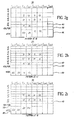
- the image sensor 5 of the present invention includes the array of pixels 20, a transition region 30 electrically connected to it, and a horizontal shift register 80 electrically connected to the transition region 30.
- the transition region 30 includes a first portion 40 consisting of a line or row of gates (clocked by the common timing signal labeled as V1L) and a second portion 50 also consisting of a line or row of gates in which a first mated pairs of gates 60 (see dashed line) are clocked by the common timing signal labeled as V2A and the second mated pairs of gates 70 (see solid line) are clocked by the common timing signal labeled as V2B.
- the array of pixels preferably includes a color filter spanning and covering the array for permitting electronic color representations of an image to be captured.
- a Bayer color filter array is preferably used although other color filter arrays may also be used.
- the Bayer color filter includes a repeating 2 x 2 array color pattern of:
- first portion 40 of the transition region is clocked by a first common timing signal and the second portion 50 includes a first mated pair 60 clocked by a second common timing signal and a second mated pair 70 clocked by a third common timing signal.
- a horizontal charge-coupled device (HCCD) 80 also referred to as a horizontal shift register, is electrically connected to the second portion 50 of the transition region for receiving signals from the second portion 50. It is noted that the HCCD 80 can shift charge bi-directionally.
- a plurality of lateral overflow channels 90 are connected to the HCCD 80 and coupled to a lateral overflow drain 100 for removing charge from the HCCD that exceeds its capacity. See US Patents 5,130,774 and 6,624,453 for further details on the construction and operation of lateral overflow drains.
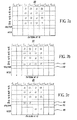
- the array 20 is shown having an image signal in only a portion of the array (a 4 x 4 array of pixels) for clarity of understanding. It is well known and to be understood that each pixel includes a signal therein. The below described operation is to be performed for all the pixels of the array in the same manner.
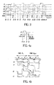
- a timing diagram for Figs. 2a - 2r is shown respectively in Fig. 3 .
- This timing diagram facilitates understanding of the timing and more specifically the "common timing signal.”
- the image is captured in the array of pixels 20 as shown in Fig. 2a (only 16 pixels with the image signal are shown for clarity) and the last row of signal or charge is transferred to the first portion 40 of the transition region as shown in Fig. 2b .
- the second mated pair 70 of Gr and R colors in the first portion 40 are then shifted into the second portion 50 and the HCCD 80 and eventually into only the HCCD 80.
- the V1L gate 40 is sized appropriately to hold the full capacity of one pixel while the voltage applied to the V1L gate is at the low voltage level.
- the second mated pair 70 of Gr and R charge in the HCCD 80 is shifted left until it respectively aligns with the first mated pair 60 of Gr and R charge remaining in the first portion 40.
- the Gr and R charges in the first portion 40 are shifted down into the second portion 50 and HCCD 80 so that they are binned or combined together (2Gr and 2R), and all the other lines in the array are also shifted down in the pixel array 20 into the next gate V2.
- the combined charge is then shifted entirely into the HCCD 80 and the next line of charge from the array is shifted into the first portion 40.
- the second mated pair 70 of B and Gb charges are shifted into the second portion 50 and the corresponding HCCD 80.
- all the B and Gb charge is shifted into the HCCD 80 and shifted left so that the B and Gb charge are aligned with the same color in the first portion.
- the first mated pair 60 of B and Gb charge in the first portion 40 is shifted into the second portion 50 and HCCD 80 so that B and Gb are combined.
- the combined B and Gb charge (2B and 2Gb) is shifted entirely into the HCCD 80 as shown in 2j, and the next line of charge from the pixel array 20 is shifted into the first portion 40 while the charge in the HCCD 80 is shifted right so that the Gr and R in the HCCD 80 is aligned with the same color in the first portion 40.
- the first mated pair 60 of Gr and R charge in the first portion 40 is shifted into the second portion 50 and the HCCD 80 so that the 2Gr and 2R charge is respectively combined with a Gr and R to form a combined 3Gr and 3R charge.
- the 3Gr and 3R charge is shifted entirely into the HCCD 80 and all the charge in the HCCD 80 is shifted to the right so that the Gr and R charge are again aligned with the second mated pair 70 of Gr and R charge in the first portion 40.
- the second mated pair 70 of Gr and R charge in the first portion 40 is shifted into the corresponding second portion 50 and HCCD 80 so that the 3Gr and 3R charge is combined with a Gr and R charge for forming a 4Gr and 4R charge.
- the 4Gr and 4R charge is shifted entirely into the HCCD 80, and all the charge in the HCCD 80 is shifted left so that the 2B and 2Gb in the HCCD 80 is aligned with the second mated pair 70 of B and Gb charge in the first portion 40.
- the second mated pair 70 of B and Gb charge in the first portion 40 is shifted into the corresponding second portion 50 and HCCD 80 so that the B and Gb are combined for forming a 3B and 3Gb charge.
- the second mated pair 70 of B and Gb charge in the second portion 50 is shifted entirely into the HCCD 80 and all the charge in the HCCD 80 is shifted left so that the B and Gb charges in the first portion 40 are aligned with the same colors in the HCCD 80.
- the first mated pair 60 of B and Gb charge is then shifted into the second portion 50 and HCCD 80 so that 4B and 4Gb are formed as shown in Fig. 2q .
- the charge in the second portion 50 is shifted entirely into the HCCD 80 and the charge in the HCCD 80 can then be shifted out of the HCCD 80 for processing as is well known in the art.
- FIG. 3 there is shown the timing diagram for the image sensor 5 (V1 and V2), transitions regions 30 (V1L, V2A and V2B) and HCCD 80 (Hclks) for performing on-chip pixel binning.
- the simplified Hclks timing pattern is used to represent the operation of all phases of the HCCD 80.
- the notation L2 represents shifting pixels in the HCCD 80 left two columns relative to the pixel array 20.
- R2 represents shifting pixels in the HCCD 80 right two columns relative to the pixel array 20.
- Fig. 4a illustrates the true two-phase clocking method of the image sensor 5 (discussed hereinabove) and applies to the charge transfer of the array of pixels 20 and transition region 30 while in full resolution readout.
Landscapes
- Engineering & Computer Science (AREA)
- Multimedia (AREA)
- Signal Processing (AREA)
- Solid State Image Pick-Up Elements (AREA)
- Transforming Light Signals Into Electric Signals (AREA)
Applications Claiming Priority (2)
| Application Number | Priority Date | Filing Date | Title |
|---|---|---|---|
| US11/680,078 US7893981B2 (en) | 2007-02-28 | 2007-02-28 | Image sensor with variable resolution and sensitivity |
| PCT/US2008/002237 WO2008106035A1 (en) | 2007-02-28 | 2008-02-20 | Image sensor with variable resolution and sensitivity |
Publications (2)
| Publication Number | Publication Date |
|---|---|
| EP2119225A1 EP2119225A1 (en) | 2009-11-18 |
| EP2119225B1 true EP2119225B1 (en) | 2012-10-24 |
Family
ID=39336237
Family Applications (1)
| Application Number | Title | Priority Date | Filing Date |
|---|---|---|---|
| EP08725830A Not-in-force EP2119225B1 (en) | 2007-02-28 | 2008-02-20 | Image sensor with variable resolution and sensitivity |
Country Status (4)
| Country | Link |
|---|---|
| US (1) | US7893981B2 (enExample) |
| EP (1) | EP2119225B1 (enExample) |
| JP (1) | JP2010520662A (enExample) |
| WO (1) | WO2008106035A1 (enExample) |
Families Citing this family (8)
| Publication number | Priority date | Publication date | Assignee | Title |
|---|---|---|---|---|
| US7965326B2 (en) * | 2006-09-27 | 2011-06-21 | Fujifilm Corporation | Semiconductor element, method of driving semiconductor element and solid imaging apparatus |
| US7948534B2 (en) * | 2008-10-22 | 2011-05-24 | Eastman Kodak Company | Charge-coupled device image sensor with vertical binning of same-color pixels |
| US8164669B2 (en) * | 2008-12-19 | 2012-04-24 | Truesense Imaging, Inc. | Charge-coupled device image sensor with efficient binning of same-color pixels |
| US8749686B2 (en) | 2011-04-29 | 2014-06-10 | Truesense Imaging, Inc. | CCD image sensors and methods |
| US8724003B2 (en) | 2012-08-14 | 2014-05-13 | Truesense Imaging, Inc. | Multimode interline CCD imaging methods |
| RU2612191C1 (ru) * | 2016-02-05 | 2017-03-03 | Акционерное общество "Научно-исследовательский институт телевидения" | Видеосистема на кристалле с адаптацией к сюжету |
| EP3229172A1 (en) * | 2016-04-04 | 2017-10-11 | Conti Temic microelectronic GmbH | Driver assistance system with variable image resolution |
| RU2683241C1 (ru) * | 2018-03-02 | 2019-03-27 | Вячеслав Михайлович Смелков | Способ управления поэлементным переносом зарядовых пакетов в "кольцевом" фотоприёмнике на ПЗС для панорамного телевизионно-компьютерного наблюдения |
Family Cites Families (19)
| Publication number | Priority date | Publication date | Assignee | Title |
|---|---|---|---|---|
| US4599657A (en) * | 1981-12-29 | 1986-07-08 | Canon Kabushiki Kaisha | Image pick-up device |
| US4613402A (en) * | 1985-07-01 | 1986-09-23 | Eastman Kodak Company | Method of making edge-aligned implants and electrodes therefor |
| US5130774A (en) * | 1990-07-12 | 1992-07-14 | Eastman Kodak Company | Antiblooming structure for solid-state image sensor |
| JP3511772B2 (ja) * | 1995-12-21 | 2004-03-29 | ソニー株式会社 | 固体撮像素子、固体撮像素子の駆動方法、カメラ装置及びカメラシステム |
| KR100192328B1 (ko) * | 1996-04-03 | 1999-06-15 | 구본준 | 양방향 수평전하 전송소자 |
| JPH11234569A (ja) * | 1998-02-13 | 1999-08-27 | Sony Corp | 固体撮像装置の駆動方法及び固体撮像素子、並びにカメラ |
| JP4140077B2 (ja) * | 1998-02-18 | 2008-08-27 | ソニー株式会社 | 固体撮像素子の駆動方法及び固体撮像素子、並びにカメラ |
| KR100344505B1 (ko) * | 1998-11-30 | 2002-07-24 | 가부시끼가이샤 도시바 | 고체 이미징 장치 |
| US6624453B2 (en) * | 2001-08-31 | 2003-09-23 | Eastman Kodak Company | Lateral overflow drain, anti-blooming structure for CCD devices having improved breakdown voltage |
| JP3848650B2 (ja) * | 2002-11-12 | 2006-11-22 | 松下電器産業株式会社 | 固体撮像素子およびこれを備えたカメラ |
| JP4212095B2 (ja) * | 2003-07-15 | 2009-01-21 | シャープ株式会社 | 固体撮像装置およびその駆動方法 |
| JP4658470B2 (ja) * | 2003-11-28 | 2011-03-23 | パナソニック株式会社 | 固体撮像素子、固体撮像装置及びカメラ |
| US20050280726A1 (en) * | 2004-06-18 | 2005-12-22 | Eastman Kodak Company | Image sensor for still or video photography |
| US7538807B2 (en) * | 2004-11-23 | 2009-05-26 | Dalsa Corporation | Method and apparatus for in a multi-pixel pick-up element reducing a pixel-based resolution and/or effecting anti-aliasing through selectively combining selective primary pixel outputs to combined secondary pixel outputs |
| US7379107B2 (en) * | 2004-12-10 | 2008-05-27 | Eastman Kodak Company | Image sensor for still or video photography |
| JP4457961B2 (ja) * | 2005-04-28 | 2010-04-28 | ソニー株式会社 | 固体撮像素子 |
| US7750964B2 (en) * | 2005-09-30 | 2010-07-06 | Sony Corporation | Method and apparatus for driving a semiconductor device including driving of signal charges within and outside an effective transfer period |
| JP4833722B2 (ja) * | 2006-04-25 | 2011-12-07 | パナソニック株式会社 | 撮像装置、固体撮像装置および撮像装置の駆動方法 |
| US7948534B2 (en) * | 2008-10-22 | 2011-05-24 | Eastman Kodak Company | Charge-coupled device image sensor with vertical binning of same-color pixels |
-
2007
- 2007-02-28 US US11/680,078 patent/US7893981B2/en not_active Expired - Fee Related
-
2008
- 2008-02-20 WO PCT/US2008/002237 patent/WO2008106035A1/en not_active Ceased
- 2008-02-20 EP EP08725830A patent/EP2119225B1/en not_active Not-in-force
- 2008-02-20 JP JP2009551679A patent/JP2010520662A/ja active Pending
Also Published As
| Publication number | Publication date |
|---|---|
| EP2119225A1 (en) | 2009-11-18 |
| WO2008106035A1 (en) | 2008-09-04 |
| US7893981B2 (en) | 2011-02-22 |
| JP2010520662A (ja) | 2010-06-10 |
| US20080204585A1 (en) | 2008-08-28 |
Similar Documents
| Publication | Publication Date | Title |
|---|---|---|
| EP2119225B1 (en) | Image sensor with variable resolution and sensitivity | |
| KR100979197B1 (ko) | 고체촬상장치 | |
| US8717471B2 (en) | Solid-state imaging device applied to CMOS image sensor | |
| EP2338283B1 (en) | Image sensor with vertical binning of pixels | |
| JP2007531351A (ja) | 電荷ビニング型イメージセンサ | |
| US7379107B2 (en) | Image sensor for still or video photography | |
| US20100208116A1 (en) | Color ccd linear image sensor | |
| JP2009521842A (ja) | 静止画またはビデオ撮影用画像センサ | |
| US10616535B1 (en) | Sub-sampled color channel readout wiring for vertical detector pixel sensors | |
| KR101293385B1 (ko) | Cmos 이미지 센서 및 이를 포함하는 디지털 카메라 | |
| KR100671922B1 (ko) | 촬상 장치 및 촬상 장치의 제어 장치 | |
| EP1708483B1 (en) | Solid state imaging apparatus and driving method of the solid state imaging apparatus | |
| EP1874044B1 (en) | Solid state imaging device | |
| JP4303950B2 (ja) | 電荷転送素子の駆動方法及び固体撮像素子の駆動方法 | |
| JP4371851B2 (ja) | 撮像装置及び撮像装置の制御装置 | |
| JP2000197065A (ja) | カラーccd固体撮像素子とその駆動方法 | |
| JP2001157119A (ja) | 固体撮像装置の駆動方法 | |
| JPH09129861A (ja) | 固体撮像素子 | |
| CN101010938A (zh) | 用于静态或视频摄影的图像传感器 | |
| JP2008098834A (ja) | 撮像素子 | |
| JP2005252409A (ja) | 撮像装置及び撮像装置の制御装置 | |
| JPS61127279A (ja) | 固体イメ−ジセンサ | |
| JP2004146955A (ja) | 固体撮像素子及びその駆動方法 |
Legal Events
| Date | Code | Title | Description |
|---|---|---|---|
| PUAI | Public reference made under article 153(3) epc to a published international application that has entered the european phase |
Free format text: ORIGINAL CODE: 0009012 |
|
| 17P | Request for examination filed |
Effective date: 20090810 |
|
| AK | Designated contracting states |
Kind code of ref document: A1 Designated state(s): AT BE BG CH CY CZ DE DK EE ES FI FR GB GR HR HU IE IS IT LI LT LU LV MC MT NL NO PL PT RO SE SI SK TR |
|
| DAX | Request for extension of the european patent (deleted) | ||
| RAP1 | Party data changed (applicant data changed or rights of an application transferred) |
Owner name: TRUESENCE IMAGING, INC. |
|
| RAP1 | Party data changed (applicant data changed or rights of an application transferred) |
Owner name: TRUESENSE IMAGING, INC. |
|
| 17Q | First examination report despatched |
Effective date: 20120224 |
|
| GRAP | Despatch of communication of intention to grant a patent |
Free format text: ORIGINAL CODE: EPIDOSNIGR1 |
|
| RIC1 | Information provided on ipc code assigned before grant |
Ipc: H04N 5/335 20110101AFI20120511BHEP |
|
| GRAS | Grant fee paid |
Free format text: ORIGINAL CODE: EPIDOSNIGR3 |
|
| GRAA | (expected) grant |
Free format text: ORIGINAL CODE: 0009210 |
|
| AK | Designated contracting states |
Kind code of ref document: B1 Designated state(s): AT BE BG CH CY CZ DE DK EE ES FI FR GB GR HR HU IE IS IT LI LT LU LV MC MT NL NO PL PT RO SE SI SK TR |
|
| REG | Reference to a national code |
Ref country code: GB Ref legal event code: FG4D |
|
| REG | Reference to a national code |
Ref country code: CH Ref legal event code: EP |
|
| REG | Reference to a national code |
Ref country code: AT Ref legal event code: REF Ref document number: 581436 Country of ref document: AT Kind code of ref document: T Effective date: 20121115 |
|
| REG | Reference to a national code |
Ref country code: IE Ref legal event code: FG4D |
|
| REG | Reference to a national code |
Ref country code: DE Ref legal event code: R096 Ref document number: 602008019594 Country of ref document: DE Effective date: 20121220 |
|
| REG | Reference to a national code |
Ref country code: AT Ref legal event code: MK05 Ref document number: 581436 Country of ref document: AT Kind code of ref document: T Effective date: 20121024 |
|
| REG | Reference to a national code |
Ref country code: NL Ref legal event code: VDEP Effective date: 20121024 |
|
| PG25 | Lapsed in a contracting state [announced via postgrant information from national office to epo] |
Ref country code: SE Free format text: LAPSE BECAUSE OF FAILURE TO SUBMIT A TRANSLATION OF THE DESCRIPTION OR TO PAY THE FEE WITHIN THE PRESCRIBED TIME-LIMIT Effective date: 20121024 Ref country code: IS Free format text: LAPSE BECAUSE OF FAILURE TO SUBMIT A TRANSLATION OF THE DESCRIPTION OR TO PAY THE FEE WITHIN THE PRESCRIBED TIME-LIMIT Effective date: 20130224 Ref country code: NO Free format text: LAPSE BECAUSE OF FAILURE TO SUBMIT A TRANSLATION OF THE DESCRIPTION OR TO PAY THE FEE WITHIN THE PRESCRIBED TIME-LIMIT Effective date: 20130124 Ref country code: NL Free format text: LAPSE BECAUSE OF FAILURE TO SUBMIT A TRANSLATION OF THE DESCRIPTION OR TO PAY THE FEE WITHIN THE PRESCRIBED TIME-LIMIT Effective date: 20121024 Ref country code: FI Free format text: LAPSE BECAUSE OF FAILURE TO SUBMIT A TRANSLATION OF THE DESCRIPTION OR TO PAY THE FEE WITHIN THE PRESCRIBED TIME-LIMIT Effective date: 20121024 Ref country code: ES Free format text: LAPSE BECAUSE OF FAILURE TO SUBMIT A TRANSLATION OF THE DESCRIPTION OR TO PAY THE FEE WITHIN THE PRESCRIBED TIME-LIMIT Effective date: 20130204 Ref country code: HR Free format text: LAPSE BECAUSE OF FAILURE TO SUBMIT A TRANSLATION OF THE DESCRIPTION OR TO PAY THE FEE WITHIN THE PRESCRIBED TIME-LIMIT Effective date: 20121024 |
|
| PG25 | Lapsed in a contracting state [announced via postgrant information from national office to epo] |
Ref country code: PT Free format text: LAPSE BECAUSE OF FAILURE TO SUBMIT A TRANSLATION OF THE DESCRIPTION OR TO PAY THE FEE WITHIN THE PRESCRIBED TIME-LIMIT Effective date: 20130225 Ref country code: LV Free format text: LAPSE BECAUSE OF FAILURE TO SUBMIT A TRANSLATION OF THE DESCRIPTION OR TO PAY THE FEE WITHIN THE PRESCRIBED TIME-LIMIT Effective date: 20121024 Ref country code: GR Free format text: LAPSE BECAUSE OF FAILURE TO SUBMIT A TRANSLATION OF THE DESCRIPTION OR TO PAY THE FEE WITHIN THE PRESCRIBED TIME-LIMIT Effective date: 20130125 Ref country code: CY Free format text: LAPSE BECAUSE OF FAILURE TO SUBMIT A TRANSLATION OF THE DESCRIPTION OR TO PAY THE FEE WITHIN THE PRESCRIBED TIME-LIMIT Effective date: 20121024 Ref country code: SI Free format text: LAPSE BECAUSE OF FAILURE TO SUBMIT A TRANSLATION OF THE DESCRIPTION OR TO PAY THE FEE WITHIN THE PRESCRIBED TIME-LIMIT Effective date: 20121024 Ref country code: PL Free format text: LAPSE BECAUSE OF FAILURE TO SUBMIT A TRANSLATION OF THE DESCRIPTION OR TO PAY THE FEE WITHIN THE PRESCRIBED TIME-LIMIT Effective date: 20121024 Ref country code: BE Free format text: LAPSE BECAUSE OF FAILURE TO SUBMIT A TRANSLATION OF THE DESCRIPTION OR TO PAY THE FEE WITHIN THE PRESCRIBED TIME-LIMIT Effective date: 20121024 |
|
| PG25 | Lapsed in a contracting state [announced via postgrant information from national office to epo] |
Ref country code: AT Free format text: LAPSE BECAUSE OF FAILURE TO SUBMIT A TRANSLATION OF THE DESCRIPTION OR TO PAY THE FEE WITHIN THE PRESCRIBED TIME-LIMIT Effective date: 20121024 |
|
| PG25 | Lapsed in a contracting state [announced via postgrant information from national office to epo] |
Ref country code: DK Free format text: LAPSE BECAUSE OF FAILURE TO SUBMIT A TRANSLATION OF THE DESCRIPTION OR TO PAY THE FEE WITHIN THE PRESCRIBED TIME-LIMIT Effective date: 20121024 Ref country code: BG Free format text: LAPSE BECAUSE OF FAILURE TO SUBMIT A TRANSLATION OF THE DESCRIPTION OR TO PAY THE FEE WITHIN THE PRESCRIBED TIME-LIMIT Effective date: 20130124 Ref country code: EE Free format text: LAPSE BECAUSE OF FAILURE TO SUBMIT A TRANSLATION OF THE DESCRIPTION OR TO PAY THE FEE WITHIN THE PRESCRIBED TIME-LIMIT Effective date: 20121024 Ref country code: CZ Free format text: LAPSE BECAUSE OF FAILURE TO SUBMIT A TRANSLATION OF THE DESCRIPTION OR TO PAY THE FEE WITHIN THE PRESCRIBED TIME-LIMIT Effective date: 20121024 Ref country code: SK Free format text: LAPSE BECAUSE OF FAILURE TO SUBMIT A TRANSLATION OF THE DESCRIPTION OR TO PAY THE FEE WITHIN THE PRESCRIBED TIME-LIMIT Effective date: 20121024 |
|
| PG25 | Lapsed in a contracting state [announced via postgrant information from national office to epo] |
Ref country code: IT Free format text: LAPSE BECAUSE OF FAILURE TO SUBMIT A TRANSLATION OF THE DESCRIPTION OR TO PAY THE FEE WITHIN THE PRESCRIBED TIME-LIMIT Effective date: 20121024 Ref country code: RO Free format text: LAPSE BECAUSE OF FAILURE TO SUBMIT A TRANSLATION OF THE DESCRIPTION OR TO PAY THE FEE WITHIN THE PRESCRIBED TIME-LIMIT Effective date: 20121024 |
|
| PLBE | No opposition filed within time limit |
Free format text: ORIGINAL CODE: 0009261 |
|
| STAA | Information on the status of an ep patent application or granted ep patent |
Free format text: STATUS: NO OPPOSITION FILED WITHIN TIME LIMIT |
|
| PG25 | Lapsed in a contracting state [announced via postgrant information from national office to epo] |
Ref country code: MC Free format text: LAPSE BECAUSE OF NON-PAYMENT OF DUE FEES Effective date: 20130228 |
|
| REG | Reference to a national code |
Ref country code: CH Ref legal event code: PL |
|
| 26N | No opposition filed |
Effective date: 20130725 |
|
| PG25 | Lapsed in a contracting state [announced via postgrant information from national office to epo] |
Ref country code: CH Free format text: LAPSE BECAUSE OF NON-PAYMENT OF DUE FEES Effective date: 20130228 Ref country code: LI Free format text: LAPSE BECAUSE OF NON-PAYMENT OF DUE FEES Effective date: 20130228 |
|
| REG | Reference to a national code |
Ref country code: FR Ref legal event code: ST Effective date: 20131031 |
|
| REG | Reference to a national code |
Ref country code: DE Ref legal event code: R097 Ref document number: 602008019594 Country of ref document: DE Effective date: 20130725 |
|
| REG | Reference to a national code |
Ref country code: IE Ref legal event code: MM4A |
|
| PG25 | Lapsed in a contracting state [announced via postgrant information from national office to epo] |
Ref country code: IE Free format text: LAPSE BECAUSE OF NON-PAYMENT OF DUE FEES Effective date: 20130220 Ref country code: FR Free format text: LAPSE BECAUSE OF NON-PAYMENT OF DUE FEES Effective date: 20130228 |
|
| PG25 | Lapsed in a contracting state [announced via postgrant information from national office to epo] |
Ref country code: LT Free format text: LAPSE BECAUSE OF FAILURE TO SUBMIT A TRANSLATION OF THE DESCRIPTION OR TO PAY THE FEE WITHIN THE PRESCRIBED TIME-LIMIT Effective date: 20121024 Ref country code: MT Free format text: LAPSE BECAUSE OF FAILURE TO SUBMIT A TRANSLATION OF THE DESCRIPTION OR TO PAY THE FEE WITHIN THE PRESCRIBED TIME-LIMIT Effective date: 20121024 |
|
| REG | Reference to a national code |
Ref country code: GB Ref legal event code: 732E Free format text: REGISTERED BETWEEN 20140904 AND 20140910 |
|
| REG | Reference to a national code |
Ref country code: DE Ref legal event code: R082 Ref document number: 602008019594 Country of ref document: DE Representative=s name: MEYER & PARTNER GBR, DE |
|
| REG | Reference to a national code |
Ref country code: DE Ref legal event code: R082 Ref document number: 602008019594 Country of ref document: DE Representative=s name: MEYER & PARTNER GBR, DE Effective date: 20141121 Ref country code: DE Ref legal event code: R081 Ref document number: 602008019594 Country of ref document: DE Owner name: SEMICONDUCTOR COMPONENTS INDUSTRIES, LLC (N. D, US Free format text: FORMER OWNER: TRUESENSE IMAGING, INC, WILMINGTON, DEL., US Effective date: 20141121 |
|
| PG25 | Lapsed in a contracting state [announced via postgrant information from national office to epo] |
Ref country code: TR Free format text: LAPSE BECAUSE OF FAILURE TO SUBMIT A TRANSLATION OF THE DESCRIPTION OR TO PAY THE FEE WITHIN THE PRESCRIBED TIME-LIMIT Effective date: 20121024 |
|
| PG25 | Lapsed in a contracting state [announced via postgrant information from national office to epo] |
Ref country code: LU Free format text: LAPSE BECAUSE OF NON-PAYMENT OF DUE FEES Effective date: 20130220 Ref country code: HU Free format text: LAPSE BECAUSE OF FAILURE TO SUBMIT A TRANSLATION OF THE DESCRIPTION OR TO PAY THE FEE WITHIN THE PRESCRIBED TIME-LIMIT; INVALID AB INITIO Effective date: 20080220 |
|
| PGFP | Annual fee paid to national office [announced via postgrant information from national office to epo] |
Ref country code: DE Payment date: 20210120 Year of fee payment: 14 Ref country code: GB Payment date: 20210120 Year of fee payment: 14 |
|
| REG | Reference to a national code |
Ref country code: DE Ref legal event code: R119 Ref document number: 602008019594 Country of ref document: DE |
|
| GBPC | Gb: european patent ceased through non-payment of renewal fee |
Effective date: 20220220 |
|
| PG25 | Lapsed in a contracting state [announced via postgrant information from national office to epo] |
Ref country code: GB Free format text: LAPSE BECAUSE OF NON-PAYMENT OF DUE FEES Effective date: 20220220 Ref country code: DE Free format text: LAPSE BECAUSE OF NON-PAYMENT OF DUE FEES Effective date: 20220901 |