EP2107745A1 - Verfahren und System zur Bitpolarisierungscodierung - Google Patents
Verfahren und System zur Bitpolarisierungscodierung Download PDFInfo
- Publication number
- EP2107745A1 EP2107745A1 EP09157010A EP09157010A EP2107745A1 EP 2107745 A1 EP2107745 A1 EP 2107745A1 EP 09157010 A EP09157010 A EP 09157010A EP 09157010 A EP09157010 A EP 09157010A EP 2107745 A1 EP2107745 A1 EP 2107745A1
- Authority
- EP
- European Patent Office
- Prior art keywords
- binary bits
- digital code
- digital
- analog signal
- bits
- Prior art date
- Legal status (The legal status is an assumption and is not a legal conclusion. Google has not performed a legal analysis and makes no representation as to the accuracy of the status listed.)
- Granted
Links
Images


Classifications
-
- H—ELECTRICITY
- H03—ELECTRONIC CIRCUITRY
- H03M—CODING; DECODING; CODE CONVERSION IN GENERAL
- H03M1/00—Analogue/digital conversion; Digital/analogue conversion
- H03M1/06—Continuously compensating for, or preventing, undesired influence of physical parameters
- H03M1/08—Continuously compensating for, or preventing, undesired influence of physical parameters of noise
- H03M1/0863—Continuously compensating for, or preventing, undesired influence of physical parameters of noise of switching transients, e.g. glitches
-
- H—ELECTRICITY
- H03—ELECTRONIC CIRCUITRY
- H03M—CODING; DECODING; CODE CONVERSION IN GENERAL
- H03M7/00—Conversion of a code where information is represented by a given sequence or number of digits to a code where the same, similar or subset of information is represented by a different sequence or number of digits
- H03M7/02—Conversion to or from weighted codes, i.e. the weight given to a digit depending on the position of the digit within the block or code word
- H03M7/04—Conversion to or from weighted codes, i.e. the weight given to a digit depending on the position of the digit within the block or code word the radix thereof being two
-
- H—ELECTRICITY
- H03—ELECTRONIC CIRCUITRY
- H03M—CODING; DECODING; CODE CONVERSION IN GENERAL
- H03M7/00—Conversion of a code where information is represented by a given sequence or number of digits to a code where the same, similar or subset of information is represented by a different sequence or number of digits
- H03M7/14—Conversion to or from non-weighted codes
-
- H—ELECTRICITY
- H04—ELECTRIC COMMUNICATION TECHNIQUE
- H04L—TRANSMISSION OF DIGITAL INFORMATION, e.g. TELEGRAPHIC COMMUNICATION
- H04L25/00—Baseband systems
- H04L25/38—Synchronous or start-stop systems, e.g. for Baudot code
- H04L25/40—Transmitting circuits; Receiving circuits
- H04L25/49—Transmitting circuits; Receiving circuits using code conversion at the transmitter; using predistortion; using insertion of idle bits for obtaining a desired frequency spectrum; using three or more amplitude levels ; Baseband coding techniques specific to data transmission systems
- H04L25/4906—Transmitting circuits; Receiving circuits using code conversion at the transmitter; using predistortion; using insertion of idle bits for obtaining a desired frequency spectrum; using three or more amplitude levels ; Baseband coding techniques specific to data transmission systems using binary codes
- H04L25/4915—Transmitting circuits; Receiving circuits using code conversion at the transmitter; using predistortion; using insertion of idle bits for obtaining a desired frequency spectrum; using three or more amplitude levels ; Baseband coding techniques specific to data transmission systems using binary codes using pattern inversion or substitution
Definitions
- teachings presented herein relate to electronic circuitry. More specifically, the teachings relate to methods and systems for digital data coding and electronic circuits incorporating the same.
- A/D and D/A converters are widely used in the industry of electronics.
- the analog signal is sampled at discrete points according to a certain frequency. Voltages of the analog signal at such sampled points are measured. Each measured voltage at a sampling point is then coded using a digital code having a plurality of binary bits.
- a digital code can be used to represent the sampled analog value and can be transmitted in a digital means to a destination.
- the digital code can be decoded by a D/A converter to derive an estimated voltage that is similar to the original voltage being coded.
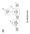
- Fig. 1(a) shows a typical A/D and D/A processing flow. In Fig.
- an A/D converter 110 takes an analog signal A as input and generates a digital code B as an output.
- the digital code B is often processed by a digital signal processor 115 to generate a digital signal C.
- digital signal C is transmitted and received by a receiver 120, which may then apply a D/A process at a D/A converter 130 and produces a recovered analog signal C' based on digital signal C.
- a digital code representing a particular sampled voltage of the analog signal is conventionally determined, by the A/D converter 110 based on a look-up table in accordance with the voltage level of the sample.
- Fig. 1(b) depicts a typical A/D converter 110.
- An analog signal A is sampled first by an analog sampling unit 140 to produce individual analog voltages as an output.
- an A/D look-up unit 150 determines a digital code representing the analog voltage based on a look-up table 160.
- a D/A converter reverses the process to convert a digital code to generate an analog voltage represented by the digital code. This is shown in Fig. 1(c) (Prior Art), where a D/A look-up unit 170 in a D/A converter 130 consults with the look-up table 160 based on a received digital code C to produce an analog voltage. The represented analog voltage is then sent to an analog signal generator 180, which may utilize different analog voltages to produce an estimated analog signal C'.
- Fig. 1(d) shows an exemplary look-up table 160 in which the left column 190 lists various ranges of analog voltages and, correspondingly, the right column 195 provides 14-bit digital codes for different voltage ranges. For instance, for a zero voltage, the digital code is "00 0000 0000 0000". For a voltage between +0.000122v and +0.000244v, the corresponding digital code is "00 0000 0000 0001". For a voltage between -0.000122v and -0.000244, the corresponding digital code is "11 1111 1111 1111", etc.
- a previous solution for reducing digital noise is Gray Coding, as disclosed in U.S. Patent No. 2,632,058 issued to F. Gray .
- This method solves the problem by allowing only one bit changing state between any two adjacent codes.
- a disadvantage of this approach is that its implementation requires complex circuitry for coding and decoding data. Therefore, a solution that both reduces digital noise and is cost effective is needed.
- Fig. 1(a)-(d) Prior Art
- Fig. 1(a)-(d) Prior Art
- Fig. 2 depicts a high level block diagram for bit polarization format coding, according to an embodiment of the present teaching
- Fig. 3 shows a conversion table facilitating transformations from an analog voltage to a digital code and from a digital code to a modified digital code using bit polarization format, according to an embodiment of the present teaching
- Fig. 4 depicts a block diagram 400 incorporating BPF coding in the context of A/D and D/A flow, according to an embodiment of the present teaching.
- Fig. 5(a) - (e) show different exemplary implementations of bit polarization coding according to embodiments of the present teaching.
- FIG. 2 depicts a high level block diagram 200 for bit polarization format coding, according to an embodiment of the present teaching.
- a digital code 205 is a binary code having a plurality of binary bits.
- a digital code can have 14 binary bits, each of which has a state of either 0 or 1.
- Such a binary code may be an output from an A/D converter (not shown).
- BPF bit polarization format
- the modified digital code 215 is derived by inverting a certain portion of the bit state of the digital code 205. For example, substantially one half of the bits in the digital code 205 may be inverted.
- the bit polarization format is for the purpose of balancing the number of bits that change from 0s to 1s and the number of bits that change from 1s to 0s, especially when the analog signal is a small signal.
- a BPF decoder 220 performs a reverse operation to recover the digital code 205 based on the modified digital code 215.
- the BPF coder 210 inverts a certain number of bits
- the BPF decoder 220 applies inversion to the same bits that have been inverted by the BPF coder 210.
- An exemplary BPF coding scheme is to alternate the bits to be inverted, namely alternate bit polarization format or ABPF. This ensures that one half of the bits are inverted when the total number of bits is an even number and a substantially one half of the total number of bits are inverted when the number of bits is an odd number.
- Fig. 3 illustrates an ABPF conversion table for the BPF coder 210 and BPF decoder 220.
- a conversion table facilitates transformations from an analog voltage to a digital code and from a digital code to a modified digital code using bit polarization format, according to an embodiment of the present teaching.
- the left column 190 and the middle column 195 correspond to the left column 190 and right column 195 in Fig. 1(d) .
- the right column 310 in Fig. 3 corresponds to the BPF coding.
- the modified digital code can be derived by inverting every other bit in the given digital code. For instance, for a digital code with all zeros corresponding to analog voltage 0V, the modified digital code is "10 1010 1010 1010".
- the modified digital code is "01 0101 0101 0101".
- the digital codes change from all zeros to all ones, which has the problem discussed herein. With the modified digital codes, about one half of such changes are avoided and, hence, to reduce the digital noise associated with the original digital code.
- Fig. 4 depicts a block diagram 400 incorporating BPF coding in the context of A/D and D/A flow, according to an embodiment of the present teaching.
- the block diagram structure illustrated in Fig. 4 is largely similar to what is shown in Fig. 1 except for the incorporation of the BPF coder 210 and the BPF decoder 220.
- a digital code generated by the A/D converter 110 is modified by the BPF coder 210 to generate a modified digital code according to a pre-determined coding scheme.
- a pre-determined scheme may correspond to what is illustrated in Fig. 3 or can be any coding scheme (some are shown in Fig. 5(a) - (e) ) that is appropriate.
- a receiver 410 in Fig. 4 decodes first, upon receiving the modified digital code, to recover the digital code that has been modified. Such produced digital code is then sent to the D/A converter to produce an estimate A' for the original analog voltage A.
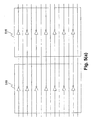
- Fig. 5(a) - (e) show different exemplary bit polarization formats according to embodiments of the present teaching.
- Fig. 5(a) shows an exemplary scheme in which alternate bits are inverted to achieve bit polarization, according to an embodiment of the present teaching.
- the left circuitry 510 represents an exemplary implementation of a BPF coder, having inverters arranged in alternate to achieve alternate bit inversion.
- the outputs of the circuit 510 collectively represent the modified digital code.
- the right circuitry 515 represents an exemplary implementation of a BPF decoder, having inverters arranged in the same configuration as in the BPF coder 510 to recover the original digital code.
- the outputs of the circuitry 515 collectively represent the decoded digital code.
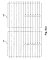
- Fig. 5(b) shows a different exemplary scheme in which about one half of the bits are inverted to achieve bit polarization, according to an embodiment of the present teaching.
- the left circuitry 520 represents an exemplary implementation of a BPF coder, having inverters arranged in the top end portion of the circuitry to invert the first one half of the bits. Such first one half may correspond to the least significant bits or most significant bits of a digital code.
- the right circuitry 525 represents an exemplary implementation of a BPF decoder, having inverters arranged in the same configuration as in the BPF coder 520 to recover the original digital code.
- Fig. 5(c) shows another different exemplary scheme in which about one half of the bits are inverted to achieve bit polarization, according to an embodiment of the present teaching.
- the left circuitry 530 represents an exemplary implementation of a BPF coder, having inverters arranged in bottom end portion of the circuitry to invert the bottom one half of the bits. Such bottom one half may correspond to the most significant bits or least significant bits of a digital code.
- the right circuitry 535 represents an exemplary implementation of a BPF decoder, having inverters arranged in the same configuration as in the BPF coder 530 to recover the original digital code.
- Fig. 5(d) shows yet another different exemplary scheme in which about one half of the bits are inverted to achieve bit polarization, according to an embodiment of the present teaching.
- the left circuitry 540 represents an exemplary implementation of a BPF coder, having inverters corresponding to about one half of the total number of bits of a digital code and arranged in a consecutive manner in any middle portion of the of the circuitry to invert corresponding one half of the bits. By middle portion, it can be anywhere as long as it does not include the least and most significant bits.
- the right circuitry 545 represents an exemplary implementation of a BPF decoder, having inverters arranged in the same configuration as in the BPF coder 540 to recover the original digital code.
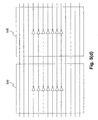
- Fig. 5(e) shows another different exemplary scheme in which about one half of the bits are inverted to achieve bit polarization, according to an embodiment of the present teaching.
- the left circuitry 550 represents an exemplary implementation of a BPF coder, having inverters corresponding to about one half of the total number of bits of a digital code and arranged in a plurality of clusters, each may have a different number of inverters and scattered in non-adjacent portions of the circuitry to invert corresponding one half of the bits.
- the right circuitry 555 represents an exemplary implementation of a BPF decoder, having inverters arranged in the same configuration as in the BPF coder 550 to recover the original digital code.
Landscapes
- Engineering & Computer Science (AREA)
- Theoretical Computer Science (AREA)
- Physics & Mathematics (AREA)
- Spectroscopy & Molecular Physics (AREA)
- Computer Networks & Wireless Communication (AREA)
- Signal Processing (AREA)
- Analogue/Digital Conversion (AREA)
Applications Claiming Priority (1)
| Application Number | Priority Date | Filing Date | Title |
|---|---|---|---|
| US12/078,384 US7656337B2 (en) | 2008-03-31 | 2008-03-31 | Method and system for bit polarization coding |
Publications (2)
| Publication Number | Publication Date |
|---|---|
| EP2107745A1 true EP2107745A1 (de) | 2009-10-07 |
| EP2107745B1 EP2107745B1 (de) | 2014-12-31 |
Family
ID=40790819
Family Applications (1)
| Application Number | Title | Priority Date | Filing Date |
|---|---|---|---|
| EP09157010.1A Active EP2107745B1 (de) | 2008-03-31 | 2009-03-31 | Verfahren und System zur Bitpolarisierungscodierung |
Country Status (4)
| Country | Link |
|---|---|
| US (1) | US7656337B2 (de) |
| EP (1) | EP2107745B1 (de) |
| CN (1) | CN101552607B (de) |
| TW (1) | TWI458265B (de) |
Families Citing this family (9)
| Publication number | Priority date | Publication date | Assignee | Title |
|---|---|---|---|---|
| WO2007135928A1 (ja) | 2006-05-21 | 2007-11-29 | Trigence Semiconductor, Inc. | デジタルアナログ変換装置 |
| JP5552620B2 (ja) | 2008-06-16 | 2014-07-16 | 株式会社 Trigence Semiconductor | デジタルスピーカー駆動装置と集中制御装置とを搭載した自動車 |
| JP5568752B2 (ja) * | 2009-12-09 | 2014-08-13 | 株式会社 Trigence Semiconductor | 選択装置 |
| CN103096217B (zh) * | 2009-12-16 | 2016-09-28 | 株式会社特瑞君思半导体 | 音响系统 |
| CN102164025B (zh) * | 2011-04-15 | 2013-06-05 | 北京邮电大学 | 基于重复编码和信道极化的编码器及其编译码方法 |
| US9083387B2 (en) | 2012-12-18 | 2015-07-14 | Samsung Electronics Co., Ltd. | Communication system with compound coding mechanism and method of operation thereof |
| US8952834B1 (en) * | 2013-02-26 | 2015-02-10 | Kandou Labs, S.A. | Methods and systems for low weight coding |
| US10312947B2 (en) * | 2016-01-21 | 2019-06-04 | Huawei Technologies Co., Ltd. | Concatenated and sliding-window polar coding |
| US10069510B2 (en) | 2016-11-21 | 2018-09-04 | Samsung Electronics Co., Ltd. | System and method for maximal code polarization |
Citations (5)
| Publication number | Priority date | Publication date | Assignee | Title |
|---|---|---|---|---|
| JPS55133158A (en) | 1979-04-04 | 1980-10-16 | Nec Corp | Pulse code communication system |
| EP0845779A2 (de) * | 1996-11-27 | 1998-06-03 | Sony United Kingdom Limited | Speicherung und Übertragung von 1-bit Daten |
| GB2319938A (en) | 1994-09-15 | 1998-06-03 | Sony Uk Ltd | Digital audio processing |
| US5830064A (en) | 1996-06-21 | 1998-11-03 | Pear, Inc. | Apparatus and method for distinguishing events which collectively exceed chance expectations and thereby controlling an output |
| US20040108945A1 (en) | 2002-11-20 | 2004-06-10 | Nec Electronics Corporation | Encoder, decoder, and data transfer system |
Family Cites Families (8)
| Publication number | Priority date | Publication date | Assignee | Title |
|---|---|---|---|---|
| JPS5875950A (ja) * | 1981-10-31 | 1983-05-07 | Sony Corp | 2値データの伝送方法 |
| KR0170259B1 (ko) * | 1993-07-26 | 1999-03-30 | 김광호 | 신호처리방법 및 장치 |
| US6229897B1 (en) * | 1997-10-30 | 2001-05-08 | Transcrypt International, Inc. | Apparatus and method of secured analog voice communication |
| KR100384886B1 (ko) * | 2000-10-10 | 2003-05-22 | 주식회사 케이티 | 니블 반전 부호 활용 방법 및 그 장치 |
| JP2002202760A (ja) * | 2000-12-27 | 2002-07-19 | Nec Corp | 液晶表示装置の駆動方法及び駆動回路 |
| DE10145722A1 (de) * | 2001-09-17 | 2003-04-24 | Infineon Technologies Ag | Konzept zur sicheren Datenkommunikation zwischen elektronischen Bausteinen |
| US20050047512A1 (en) * | 2003-08-28 | 2005-03-03 | Neff Robert M. R. | System and method using self-synchronized scrambling for reducing coherent interference |
| US7501963B1 (en) * | 2007-10-17 | 2009-03-10 | Micron Technology, Inc. | Balanced data bus inversion |
-
2008
- 2008-03-31 US US12/078,384 patent/US7656337B2/en active Active
-
2009
- 2009-03-31 CN CN200910133302.5A patent/CN101552607B/zh not_active Expired - Fee Related
- 2009-03-31 TW TW098110727A patent/TWI458265B/zh active
- 2009-03-31 EP EP09157010.1A patent/EP2107745B1/de active Active
Patent Citations (5)
| Publication number | Priority date | Publication date | Assignee | Title |
|---|---|---|---|---|
| JPS55133158A (en) | 1979-04-04 | 1980-10-16 | Nec Corp | Pulse code communication system |
| GB2319938A (en) | 1994-09-15 | 1998-06-03 | Sony Uk Ltd | Digital audio processing |
| US5830064A (en) | 1996-06-21 | 1998-11-03 | Pear, Inc. | Apparatus and method for distinguishing events which collectively exceed chance expectations and thereby controlling an output |
| EP0845779A2 (de) * | 1996-11-27 | 1998-06-03 | Sony United Kingdom Limited | Speicherung und Übertragung von 1-bit Daten |
| US20040108945A1 (en) | 2002-11-20 | 2004-06-10 | Nec Electronics Corporation | Encoder, decoder, and data transfer system |
Also Published As
| Publication number | Publication date |
|---|---|
| US7656337B2 (en) | 2010-02-02 |
| TWI458265B (zh) | 2014-10-21 |
| EP2107745B1 (de) | 2014-12-31 |
| CN101552607B (zh) | 2014-10-01 |
| CN101552607A (zh) | 2009-10-07 |
| US20090243905A1 (en) | 2009-10-01 |
| TW200950348A (en) | 2009-12-01 |
Similar Documents
| Publication | Publication Date | Title |
|---|---|---|
| US7656337B2 (en) | Method and system for bit polarization coding | |
| EP0493443B1 (de) | Paralleler ad-wandler mit 2n-1-vergleichern | |
| EP2214315A1 (de) | Verfahren und Vorrichtung zum Kodieren einer Bitfolge | |
| US7817864B2 (en) | Coding apparatus and decoding apparatus | |
| US6433725B1 (en) | High speed analog-to-digital converter | |
| GB2223369A (en) | Analogue-to-digital converters | |
| US7456774B2 (en) | Encoder circuit and A/D conversion circuit | |
| SE9604617L (sv) | Cyklisk analog-digitalomvandling | |
| CN102077468A (zh) | 混合Golomb-Elias Gamma编码方法 | |
| US9331710B1 (en) | Method and apparatus for encoding digital data into an oversampling digital to analog converter | |
| JP2007181023A (ja) | アナログデジタル変換器およびしきい値補正方法 | |
| US20210021279A1 (en) | Time-interleaved digital-to-analog converter with time-domain dynamic element matching and associated method | |
| US7999718B2 (en) | Analog-to-digital converter and electronic system including the same | |
| US9853658B1 (en) | Digital to analog converter circuit and digital to analog conversion method | |
| US7916048B2 (en) | Encoding a gray code sequence for an odd length sequence | |
| US6346906B1 (en) | Thermometric-binary code conversion method, conversion circuit therefor and encoder element circuits used therefor | |
| JPS62108663A (ja) | エントロピ−符号化方式 | |
| US6246724B1 (en) | Signal transfer method | |
| US6816098B2 (en) | High-speed oversampling modulator device | |
| JP4650485B2 (ja) | 復号装置 | |
| Im et al. | Optimal universal lossless compression with side information | |
| Prabhu et al. | Comparison of Source Coding Techniques for the Vehicle to Vehicle Communication | |
| JP5230375B2 (ja) | 画像符号化装置及び画像符号化方法 | |
| JP2009246590A (ja) | A/d変換回路 | |
| JP2789697B2 (ja) | 並列型ad変換器 |
Legal Events
| Date | Code | Title | Description |
|---|---|---|---|
| PUAI | Public reference made under article 153(3) epc to a published international application that has entered the european phase |
Free format text: ORIGINAL CODE: 0009012 |
|
| AK | Designated contracting states |
Kind code of ref document: A1 Designated state(s): AT BE BG CH CY CZ DE DK EE ES FI FR GB GR HR HU IE IS IT LI LT LU LV MC MK MT NL NO PL PT RO SE SI SK TR |
|
| AX | Request for extension of the european patent |
Extension state: AL BA RS |
|
| 17P | Request for examination filed |
Effective date: 20091013 |
|
| 17Q | First examination report despatched |
Effective date: 20091105 |
|
| AKX | Designation fees paid |
Designated state(s): AT BE BG CH CY CZ DE DK EE ES FI FR GB GR HR HU IE IS IT LI LT LU LV MC MK MT NL NO PL PT RO SE SI SK TR |
|
| APBK | Appeal reference recorded |
Free format text: ORIGINAL CODE: EPIDOSNREFNE |
|
| APBN | Date of receipt of notice of appeal recorded |
Free format text: ORIGINAL CODE: EPIDOSNNOA2E |
|
| APBR | Date of receipt of statement of grounds of appeal recorded |
Free format text: ORIGINAL CODE: EPIDOSNNOA3E |
|
| APAF | Appeal reference modified |
Free format text: ORIGINAL CODE: EPIDOSCREFNE |
|
| RAP1 | Party data changed (applicant data changed or rights of an application transferred) |
Owner name: LINEAR TECHNOLOGY CORPORATION |
|
| APBT | Appeal procedure closed |
Free format text: ORIGINAL CODE: EPIDOSNNOA9E |
|
| GRAP | Despatch of communication of intention to grant a patent |
Free format text: ORIGINAL CODE: EPIDOSNIGR1 |
|
| INTG | Intention to grant announced |
Effective date: 20140901 |
|
| RIC1 | Information provided on ipc code assigned before grant |
Ipc: H03M 7/14 20060101ALI20140818BHEP Ipc: H03M 7/04 20060101ALI20140818BHEP Ipc: H04L 25/49 20060101AFI20140818BHEP Ipc: H03M 1/08 20060101ALI20140818BHEP |
|
| GRAS | Grant fee paid |
Free format text: ORIGINAL CODE: EPIDOSNIGR3 |
|
| GRAA | (expected) grant |
Free format text: ORIGINAL CODE: 0009210 |
|
| AK | Designated contracting states |
Kind code of ref document: B1 Designated state(s): AT BE BG CH CY CZ DE DK EE ES FI FR GB GR HR HU IE IS IT LI LT LU LV MC MK MT NL NO PL PT RO SE SI SK TR |
|
| REG | Reference to a national code |
Ref country code: CH Ref legal event code: EP Ref country code: GB Ref legal event code: FG4D |
|
| REG | Reference to a national code |
Ref country code: IE Ref legal event code: FG4D |
|
| REG | Reference to a national code |
Ref country code: AT Ref legal event code: REF Ref document number: 704946 Country of ref document: AT Kind code of ref document: T Effective date: 20150215 |
|
| REG | Reference to a national code |
Ref country code: DE Ref legal event code: R096 Ref document number: 602009028639 Country of ref document: DE Effective date: 20150219 |
|
| REG | Reference to a national code |
Ref country code: NL Ref legal event code: T3 |
|
| PG25 | Lapsed in a contracting state [announced via postgrant information from national office to epo] |
Ref country code: FI Free format text: LAPSE BECAUSE OF FAILURE TO SUBMIT A TRANSLATION OF THE DESCRIPTION OR TO PAY THE FEE WITHIN THE PRESCRIBED TIME-LIMIT Effective date: 20141231 Ref country code: LT Free format text: LAPSE BECAUSE OF FAILURE TO SUBMIT A TRANSLATION OF THE DESCRIPTION OR TO PAY THE FEE WITHIN THE PRESCRIBED TIME-LIMIT Effective date: 20141231 Ref country code: NO Free format text: LAPSE BECAUSE OF FAILURE TO SUBMIT A TRANSLATION OF THE DESCRIPTION OR TO PAY THE FEE WITHIN THE PRESCRIBED TIME-LIMIT Effective date: 20150331 |
|
| REG | Reference to a national code |
Ref country code: LT Ref legal event code: MG4D |
|
| PG25 | Lapsed in a contracting state [announced via postgrant information from national office to epo] |
Ref country code: HR Free format text: LAPSE BECAUSE OF FAILURE TO SUBMIT A TRANSLATION OF THE DESCRIPTION OR TO PAY THE FEE WITHIN THE PRESCRIBED TIME-LIMIT Effective date: 20141231 Ref country code: GR Free format text: LAPSE BECAUSE OF FAILURE TO SUBMIT A TRANSLATION OF THE DESCRIPTION OR TO PAY THE FEE WITHIN THE PRESCRIBED TIME-LIMIT Effective date: 20150401 Ref country code: LV Free format text: LAPSE BECAUSE OF FAILURE TO SUBMIT A TRANSLATION OF THE DESCRIPTION OR TO PAY THE FEE WITHIN THE PRESCRIBED TIME-LIMIT Effective date: 20141231 Ref country code: SE Free format text: LAPSE BECAUSE OF FAILURE TO SUBMIT A TRANSLATION OF THE DESCRIPTION OR TO PAY THE FEE WITHIN THE PRESCRIBED TIME-LIMIT Effective date: 20141231 |
|
| REG | Reference to a national code |
Ref country code: AT Ref legal event code: MK05 Ref document number: 704946 Country of ref document: AT Kind code of ref document: T Effective date: 20141231 |
|
| PG25 | Lapsed in a contracting state [announced via postgrant information from national office to epo] |
Ref country code: RO Free format text: LAPSE BECAUSE OF FAILURE TO SUBMIT A TRANSLATION OF THE DESCRIPTION OR TO PAY THE FEE WITHIN THE PRESCRIBED TIME-LIMIT Effective date: 20141231 Ref country code: SK Free format text: LAPSE BECAUSE OF FAILURE TO SUBMIT A TRANSLATION OF THE DESCRIPTION OR TO PAY THE FEE WITHIN THE PRESCRIBED TIME-LIMIT Effective date: 20141231 Ref country code: ES Free format text: LAPSE BECAUSE OF FAILURE TO SUBMIT A TRANSLATION OF THE DESCRIPTION OR TO PAY THE FEE WITHIN THE PRESCRIBED TIME-LIMIT Effective date: 20141231 Ref country code: CZ Free format text: LAPSE BECAUSE OF FAILURE TO SUBMIT A TRANSLATION OF THE DESCRIPTION OR TO PAY THE FEE WITHIN THE PRESCRIBED TIME-LIMIT Effective date: 20141231 |
|
| PG25 | Lapsed in a contracting state [announced via postgrant information from national office to epo] |
Ref country code: PL Free format text: LAPSE BECAUSE OF FAILURE TO SUBMIT A TRANSLATION OF THE DESCRIPTION OR TO PAY THE FEE WITHIN THE PRESCRIBED TIME-LIMIT Effective date: 20141231 Ref country code: AT Free format text: LAPSE BECAUSE OF FAILURE TO SUBMIT A TRANSLATION OF THE DESCRIPTION OR TO PAY THE FEE WITHIN THE PRESCRIBED TIME-LIMIT Effective date: 20141231 Ref country code: IS Free format text: LAPSE BECAUSE OF FAILURE TO SUBMIT A TRANSLATION OF THE DESCRIPTION OR TO PAY THE FEE WITHIN THE PRESCRIBED TIME-LIMIT Effective date: 20150430 |
|
| REG | Reference to a national code |
Ref country code: DE Ref legal event code: R097 Ref document number: 602009028639 Country of ref document: DE |
|
| PG25 | Lapsed in a contracting state [announced via postgrant information from national office to epo] |
Ref country code: LU Free format text: LAPSE BECAUSE OF FAILURE TO SUBMIT A TRANSLATION OF THE DESCRIPTION OR TO PAY THE FEE WITHIN THE PRESCRIBED TIME-LIMIT Effective date: 20150331 Ref country code: EE Free format text: LAPSE BECAUSE OF FAILURE TO SUBMIT A TRANSLATION OF THE DESCRIPTION OR TO PAY THE FEE WITHIN THE PRESCRIBED TIME-LIMIT Effective date: 20141231 Ref country code: DK Free format text: LAPSE BECAUSE OF FAILURE TO SUBMIT A TRANSLATION OF THE DESCRIPTION OR TO PAY THE FEE WITHIN THE PRESCRIBED TIME-LIMIT Effective date: 20141231 Ref country code: MC Free format text: LAPSE BECAUSE OF FAILURE TO SUBMIT A TRANSLATION OF THE DESCRIPTION OR TO PAY THE FEE WITHIN THE PRESCRIBED TIME-LIMIT Effective date: 20141231 |
|
| REG | Reference to a national code |
Ref country code: CH Ref legal event code: PL |
|
| PLBE | No opposition filed within time limit |
Free format text: ORIGINAL CODE: 0009261 |
|
| STAA | Information on the status of an ep patent application or granted ep patent |
Free format text: STATUS: NO OPPOSITION FILED WITHIN TIME LIMIT |
|
| 26N | No opposition filed |
Effective date: 20151001 |
|
| REG | Reference to a national code |
Ref country code: IE Ref legal event code: MM4A |
|
| PG25 | Lapsed in a contracting state [announced via postgrant information from national office to epo] |
Ref country code: CH Free format text: LAPSE BECAUSE OF NON-PAYMENT OF DUE FEES Effective date: 20150331 Ref country code: LI Free format text: LAPSE BECAUSE OF NON-PAYMENT OF DUE FEES Effective date: 20150331 Ref country code: IE Free format text: LAPSE BECAUSE OF NON-PAYMENT OF DUE FEES Effective date: 20150331 |
|
| PG25 | Lapsed in a contracting state [announced via postgrant information from national office to epo] |
Ref country code: SI Free format text: LAPSE BECAUSE OF FAILURE TO SUBMIT A TRANSLATION OF THE DESCRIPTION OR TO PAY THE FEE WITHIN THE PRESCRIBED TIME-LIMIT Effective date: 20141231 |
|
| REG | Reference to a national code |
Ref country code: FR Ref legal event code: PLFP Year of fee payment: 8 |
|
| PG25 | Lapsed in a contracting state [announced via postgrant information from national office to epo] |
Ref country code: BE Free format text: LAPSE BECAUSE OF FAILURE TO SUBMIT A TRANSLATION OF THE DESCRIPTION OR TO PAY THE FEE WITHIN THE PRESCRIBED TIME-LIMIT Effective date: 20141231 |
|
| PG25 | Lapsed in a contracting state [announced via postgrant information from national office to epo] |
Ref country code: MT Free format text: LAPSE BECAUSE OF FAILURE TO SUBMIT A TRANSLATION OF THE DESCRIPTION OR TO PAY THE FEE WITHIN THE PRESCRIBED TIME-LIMIT Effective date: 20141231 |
|
| REG | Reference to a national code |
Ref country code: FR Ref legal event code: PLFP Year of fee payment: 9 |
|
| PG25 | Lapsed in a contracting state [announced via postgrant information from national office to epo] |
Ref country code: BG Free format text: LAPSE BECAUSE OF FAILURE TO SUBMIT A TRANSLATION OF THE DESCRIPTION OR TO PAY THE FEE WITHIN THE PRESCRIBED TIME-LIMIT Effective date: 20141231 Ref country code: HU Free format text: LAPSE BECAUSE OF FAILURE TO SUBMIT A TRANSLATION OF THE DESCRIPTION OR TO PAY THE FEE WITHIN THE PRESCRIBED TIME-LIMIT; INVALID AB INITIO Effective date: 20090331 |
|
| PG25 | Lapsed in a contracting state [announced via postgrant information from national office to epo] |
Ref country code: CY Free format text: LAPSE BECAUSE OF FAILURE TO SUBMIT A TRANSLATION OF THE DESCRIPTION OR TO PAY THE FEE WITHIN THE PRESCRIBED TIME-LIMIT Effective date: 20141231 |
|
| PG25 | Lapsed in a contracting state [announced via postgrant information from national office to epo] |
Ref country code: PT Free format text: LAPSE BECAUSE OF FAILURE TO SUBMIT A TRANSLATION OF THE DESCRIPTION OR TO PAY THE FEE WITHIN THE PRESCRIBED TIME-LIMIT Effective date: 20150501 |
|
| PG25 | Lapsed in a contracting state [announced via postgrant information from national office to epo] |
Ref country code: TR Free format text: LAPSE BECAUSE OF FAILURE TO SUBMIT A TRANSLATION OF THE DESCRIPTION OR TO PAY THE FEE WITHIN THE PRESCRIBED TIME-LIMIT Effective date: 20141231 |
|
| REG | Reference to a national code |
Ref country code: FR Ref legal event code: PLFP Year of fee payment: 10 |
|
| PG25 | Lapsed in a contracting state [announced via postgrant information from national office to epo] |
Ref country code: MK Free format text: LAPSE BECAUSE OF FAILURE TO SUBMIT A TRANSLATION OF THE DESCRIPTION OR TO PAY THE FEE WITHIN THE PRESCRIBED TIME-LIMIT Effective date: 20141231 |
|
| REG | Reference to a national code |
Ref country code: DE Ref legal event code: R082 Ref document number: 602009028639 Country of ref document: DE Representative=s name: MUELLER-BORE & PARTNER PATENTANWAELTE PARTG MB, DE Ref country code: DE Ref legal event code: R081 Ref document number: 602009028639 Country of ref document: DE Owner name: ANALOG DEVICES INTERNATIONAL UNLIMITED COMPANY, IE Free format text: FORMER OWNER: LINEAR TECHNOLOGY CORP., MILPITAS, CALIF., US Ref country code: DE Ref legal event code: R082 Ref document number: 602009028639 Country of ref document: DE Representative=s name: WITHERS & ROGERS LLP, DE |
|
| REG | Reference to a national code |
Ref country code: DE Ref legal event code: R082 Ref document number: 602009028639 Country of ref document: DE Representative=s name: WITHERS & ROGERS LLP, DE |
|
| REG | Reference to a national code |
Ref country code: GB Ref legal event code: 732E Free format text: REGISTERED BETWEEN 20211202 AND 20211209 |
|
| REG | Reference to a national code |
Ref country code: NL Ref legal event code: PD Owner name: ANALOG DEVICES INTERNATIONAL UNLIMITED COMPANY; IE Free format text: DETAILS ASSIGNMENT: CHANGE OF OWNER(S), ASSIGNMENT; FORMER OWNER NAME: LINEAR TECHNOLOGY LLC Effective date: 20211216 |
|
| PGFP | Annual fee paid to national office [announced via postgrant information from national office to epo] |
Ref country code: IT Payment date: 20220217 Year of fee payment: 14 |
|
| PGFP | Annual fee paid to national office [announced via postgrant information from national office to epo] |
Ref country code: NL Payment date: 20230221 Year of fee payment: 15 |
|
| PGFP | Annual fee paid to national office [announced via postgrant information from national office to epo] |
Ref country code: FR Payment date: 20230222 Year of fee payment: 15 |
|
| PGFP | Annual fee paid to national office [announced via postgrant information from national office to epo] |
Ref country code: GB Payment date: 20230222 Year of fee payment: 15 |
|
| PG25 | Lapsed in a contracting state [announced via postgrant information from national office to epo] |
Ref country code: IT Free format text: LAPSE BECAUSE OF NON-PAYMENT OF DUE FEES Effective date: 20230331 |
|
| REG | Reference to a national code |
Ref country code: NL Ref legal event code: MM Effective date: 20240401 |
|
| GBPC | Gb: european patent ceased through non-payment of renewal fee |
Effective date: 20240331 |
|
| PG25 | Lapsed in a contracting state [announced via postgrant information from national office to epo] |
Ref country code: NL Free format text: LAPSE BECAUSE OF NON-PAYMENT OF DUE FEES Effective date: 20240401 |
|
| PG25 | Lapsed in a contracting state [announced via postgrant information from national office to epo] |
Ref country code: NL Free format text: LAPSE BECAUSE OF NON-PAYMENT OF DUE FEES Effective date: 20240401 |
|
| PG25 | Lapsed in a contracting state [announced via postgrant information from national office to epo] |
Ref country code: GB Free format text: LAPSE BECAUSE OF NON-PAYMENT OF DUE FEES Effective date: 20240331 |
|
| PG25 | Lapsed in a contracting state [announced via postgrant information from national office to epo] |
Ref country code: FR Free format text: LAPSE BECAUSE OF NON-PAYMENT OF DUE FEES Effective date: 20240331 |
|
| PG25 | Lapsed in a contracting state [announced via postgrant information from national office to epo] |
Ref country code: GB Free format text: LAPSE BECAUSE OF NON-PAYMENT OF DUE FEES Effective date: 20240331 Ref country code: FR Free format text: LAPSE BECAUSE OF NON-PAYMENT OF DUE FEES Effective date: 20240331 |
|
| PGFP | Annual fee paid to national office [announced via postgrant information from national office to epo] |
Ref country code: DE Payment date: 20260219 Year of fee payment: 18 |