EP2104241A2 - Drahtloses Kommunikationssystem, drahtloses Kommunikationsverfahren, Übertragungsvorrichtung und Empfangsvorrichtung - Google Patents
Drahtloses Kommunikationssystem, drahtloses Kommunikationsverfahren, Übertragungsvorrichtung und Empfangsvorrichtung Download PDFInfo
- Publication number
- EP2104241A2 EP2104241A2 EP20080171984 EP08171984A EP2104241A2 EP 2104241 A2 EP2104241 A2 EP 2104241A2 EP 20080171984 EP20080171984 EP 20080171984 EP 08171984 A EP08171984 A EP 08171984A EP 2104241 A2 EP2104241 A2 EP 2104241A2
- Authority
- EP
- European Patent Office
- Prior art keywords
- transmission
- signal sequence
- symbol
- signal
- reception
- Prior art date
- Legal status (The legal status is an assumption and is not a legal conclusion. Google has not performed a legal analysis and makes no representation as to the accuracy of the status listed.)
- Withdrawn
Links
Images


Classifications
-
- H—ELECTRICITY
- H04—ELECTRIC COMMUNICATION TECHNIQUE
- H04B—TRANSMISSION
- H04B7/00—Radio transmission systems, i.e. using radiation field
- H04B7/02—Diversity systems; Multi-antenna system, i.e. transmission or reception using multiple antennas
- H04B7/04—Diversity systems; Multi-antenna system, i.e. transmission or reception using multiple antennas using two or more spaced independent antennas
- H04B7/06—Diversity systems; Multi-antenna system, i.e. transmission or reception using multiple antennas using two or more spaced independent antennas at the transmitting station
- H04B7/0613—Diversity systems; Multi-antenna system, i.e. transmission or reception using multiple antennas using two or more spaced independent antennas at the transmitting station using simultaneous transmission
-
- H—ELECTRICITY
- H04—ELECTRIC COMMUNICATION TECHNIQUE
- H04B—TRANSMISSION
- H04B7/00—Radio transmission systems, i.e. using radiation field
- H04B7/02—Diversity systems; Multi-antenna system, i.e. transmission or reception using multiple antennas
- H04B7/04—Diversity systems; Multi-antenna system, i.e. transmission or reception using multiple antennas using two or more spaced independent antennas
- H04B7/08—Diversity systems; Multi-antenna system, i.e. transmission or reception using multiple antennas using two or more spaced independent antennas at the receiving station
-
- H—ELECTRICITY
- H04—ELECTRIC COMMUNICATION TECHNIQUE
- H04B—TRANSMISSION
- H04B7/00—Radio transmission systems, i.e. using radiation field
- H04B7/02—Diversity systems; Multi-antenna system, i.e. transmission or reception using multiple antennas
- H04B7/04—Diversity systems; Multi-antenna system, i.e. transmission or reception using multiple antennas using two or more spaced independent antennas
- H04B7/0413—MIMO systems
Definitions
- the embodiment(s) discussed herein is directed to a wireless communication system, a wireless communication method, a transmission apparatus, and a reception apparatus.
- the embodiment (s) may be employed in the MIMO (Multi-Input Multi-Output) scheme as an example of a wireless communication scheme.
- MIMO Multi-Input Multi-Output
- the diversity scheme is a well-known means for reducing the deterioration of channel quality caused by this fading.
- the diversity scheme includes two types of techniques: the transmission diversity using more than one transmitter antennas; and the reception diversity using more than one receiver antennas.
- multiple antenna technology such as the MIMO technology and the array antenna technology, can be employed.
- Frequency Division Duplex FDD
- TDD Time Division Duplex
- exemplary embodiment(s) uses the following.
- the symbol series (S1y) of the second transmission stream #1 is S/P converted into two symbol series by the second S/P converter 11-1, and the two symbol series are then subj ected to orthogonalization processing performed by the second orthogonalization processor 12-1, thereby being converted into two symbol series being mutually orthogonal, which are then sent from the transmitter antennas #2 and #3.
- the signal component (S10) separated by the symbol separator 52-0 and the signal component (S11) separated by the symbol separator 52-1 are subjected to P/S conversion performed by the second P/S converter 53-1, and the result is output as the reception stream #1 corresponding to the transmission stream #1.
- the result of separation by use of the orthogonal codes #0 and #1 can be expressed by the following formulae (5) through (8).
- the pair of the above formulae (5) and (7) are equivalent to the product of the cannel matrix having the elements of the cannel values h00, h01, h20, and h21 as its elements and the transmission signal vector (S00, S10).
- the pair of the above formulae (6) and (8) are equivalent to the product of the cannel matrix having the elements of the cannel values h10, h11, h30, and h31 as its elements and the transmission vector (S01, S11).
- the pair of the formulae (5) and (7) indicates that separation between the reception symbol S00 and the reception symbol S10 is available by use of the MIMO signal separation scheme; the pair of the formulae (6) and (8) indicates that separation between the reception symbol S01 and the reception symbol S11 is available by use of the same scheme based on the pair of the formulae (5) and (7).
- the number of transmitter antennas is four (#0 through #3); the number of receiver antenna is two (#0 and #1); the number of streams is two (#0 and #1).
- the numbers should by no means be limited to those.
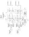
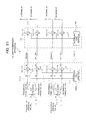
- FIG. 5 is a block diagram illustrating an example of a construction of a Code Division Multiplexing (CDM) transmission apparatus utilizing the orthogonality (orthogonal codes) of the codes as an example of the above described orthogonalization processing.
- FIG. 7 is a diagram illustrating an example of a construction of a CDM reception apparatus 50 that receives a signal sent from the CDM transmission apparatus 10 depicted in FIG. 5 .
- CDM Code Division Multiplexing
- some (transmission unit) of the blocks relating to transmission processing including: DA converters, which convert the transmission signals (symbol series) into analogue signals; frequency converters, which perform frequency conversion (up-conversion) of the analogue signals so as to have radio frequencies; and amplifiers, which amplify the wireless signals so as to have predetermined transmission power, are omitted from the illustration thereof for the sake of convenience.
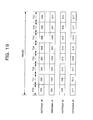
- the transmission stream #0 (S00, S01) is converted by the S/P converter 11-0 into parallel signals and becomes the symbol series #0 and #1;
- the transmission stream #1 (S10, S11) is converted by the S/P converter 11-1 into parallel signals and becomes the symbol series #2 and #3.
- the orthogonal codes can operate also as dispersion codes (channelization codes), and in that case, each of the symbol series # i is subjected to orthogonalization and dispersion (channelization) by means of being multiplied by orthogonal codes.
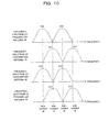
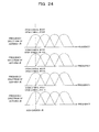
- FIG. 6 is a diagram illustrating an example of a timing chart in a case where the transmission stream is spread with orthogonal coded as described above. As indicated in the items (7) and (8), this FIG. 6 exemplifies a case in which the orthogonal code #0 per CDM symbol has a chip pattern (chip rate) of (+1, +1, +1, +1, 7) and the orthogonal code #1 per CDM symbol has a chip pattern (chip rate) of (+1, -1, +1, -1, ). In this instance, the items (1) through (12) in FIG. 6 correspond to the signals (1) through (12) in FIG. 5 .
- the signals (S00, S01) exemplified in the items (3) and (4) of FIG. 5 and FIG. 6 are multiplied by the orthogonal codes #0 and #1 having the chip pattern exemplified in the items (7) and (8) of FIG. 6 by means of the multipliers 121-0 and 121-1, respectively, thereby being orthogonalized, and becomes the signals exemplified in the items (9) and (10) of FIG. 6 .
- the signals exemplified in the items (9) through (12) of FIG. 5 and FIG. 6 are multiplied by a scrambling code generated by the scrambling code generator 130 by means of the multiplier 131-i, and the resultant signal is sent from the transmitter antenna # i .
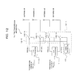
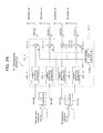
- the CDM reception apparatus 50 depicted in FIG. 7 includes, for example: two receiver antennas #0 and #1; the CDM demodulators 54-0 and 54-1 corresponding to the above receiver antennas #0 and #1, respectively; orthogonal separators 51-0 and 51-1; symbol separators 52-0 and 52-1; and P/S converters 53-0 and 53-1.
- some (reception unit) of the blocks relating to reception processing including: low-noise amplifiers, which perform low-noise amplification of the wireless signals received through the receiver antennas #0 and #1; frequency converters, which perform frequency conversion (down-conversion) of the wireless signals so as to have baseband frequencies; and AD converters, which convert the baseband signals into the digital signals, are omitted from the illustration thereof for the sake of convenience.
- the constructions of the orthogonal separators (decoders) 51-0 and 51-1 can be the same as or similar to those exemplified in FIG. 4 .
- the signal received through the receiver antenna #0 is inversely spread (demodulated) in the CDM demodulator 54-0 by use of the replica (chip pattern) of the above mentioned scrambling code, and the resultant signal is input to the orthogonal separator 51-0 as a reception signal #0 of the chip series exemplified in the item (1) of FIG. 8 .
- the signal received through the reception antenna #1 is inversely spread (demodulated) in the CDM demodulator 54-1 by use of the replica (chip pattern) of the above mentioned scrambling code, and the resultant signal is input to the orthogonal separator 51-1 as the reception signal #1 of the chip series exemplified in the item (2) of FIG. 8 .
- the signal of each chip includes the signal sent from each transmission antenna # i of the CDM transmission apparatus 10. That is, for example, as indicated in the item (3) of FIG. 8 , the chip signal r00 is expressed by the above described formula (1), and the chip signal r01 is expressed by the above describe formula (2). Likewise, as indicated in the item (4) of FIG. 8 , the chip signal r10 is expressed by the above described formula (3), and the chip signal r11 is expressed by the above described formula (4).
- each of these chip signals is multiplied by the replicas of the orthogonal codes #0 and #1 in the orthogonal separators 51-0 and 51-1, and is separated into the signal sent from the transmitter antennas #0 and #2 and the signal sent from the transmitter antennas #1 and #3.
- the chip signals r00 and r01 of the reception signal #0 are multiplied by the replica of the orthogonal code #0 at the chip cycle (+1, +1, +1, +1, ...) exemplified in the item (5) of FIG. 8 and the replica of the orthogonal code #1 at the chip cycle (+1, -1, +1, -1, 7) exemplified in the item (6) of FIG. 8 , respectively, in the multipliers 511-0 and 511-1.
- the chip signals r10 and r11 of the reception signal #1 are multiplied by the replica of the orthogonal code #0 at the chip cycle (+1, +1, +1, +1, ...) exemplified in the item (5) of FIG. 8 and the replica of the orthogonal code #1 at the chip cycle (+1, -1, +1, -1, ...) exemplified in the item (6) of FIG. 8 , respectively, in the multipliers 511-2 and 511-3.
- the symbol separator 52-0 performs MIMO signal separation by symbol unit based on the channel matrix having h00, h01, h20, and h21 as the elements thereof and the transmission signal vector (S00, S10).
- the symbol separator 52-1 performs MIMO signal separation by symbol unit based on the channel matrix having h10, h11, h30, and h31 as the elements thereof and the transmission signal vector (S01, S11).
- the reception symbol S00 and the reception symbol S01 are separated from the pair of the formulae (5) and (7); as exemplified in the items (17) and (18) of FIG. 8 , and the reception symbol S10 and the reception symbol S11 are separated from the pair of the formulae (6) and (8).
- some (transmission unit) of the blocks relating to transmission processing including: DA converters, which convert the transmission signals (symbol series) into the analogue signals; frequency converters, which perform frequency conversion (up-conversion) of the analogue signals so as to have radio frequencies; and amplifiers, which amplify the wireless signals so as to have predetermined transmission power, are omitted from the illustration thereof for the sake of convenience.
- the transmission streams #0 and #1 each are converted into two symbol series in the corresponding S/P converters 11-0 and 11-1, respectively.
- the signal (symbol) series of the transmission stream #0 is S00, S01, S02, ...
- the signal (symbol) series of the transmission stream #1 is S10, S11, S12, ....
- the transmission stream #0 is converted (divided) into the first symbol series S00, S02, ... and the second symbol series S01, S03, ....
- the first symbol series is input to the S/P converter 125-0 of the orthogonalization processor 12-0; the second symbol series is input to the S/P converter 125-1 of the mapping processor 12-0.
- the other transmission stream #1 is converted (divided) into the first symbol series S10, S12, ... and the second symbol series S11, S13, ....
- the first symbol series is input to the S/P converter 125-2 of the mapping processor 12-1; the second symbol series is input to the S/P converter 125-3 of the mapping processor 12-1.
- the mapper 126-i performs symbol mapping to frequencies (sub-carriers) in such a manner that the first symbol series and the second symbol series mutually have an orthogonal characteristic therebetween.
- the transmission symbol S10 (S12) of the transmission stream #1 is mapped to the sub-carrier #0 (#2) of the transmitter antenna #2; the transmission symbol S11 (S13) is mapped to the sub-carrier #0 (#2), which has an orthogonal characteristic in frequency with the sub-carrier #1 (#3).
- the time domain signal is converted into an OFDM symbol, which is then converted into a serial signal by the P/S converter 16-i before being sent from the corresponding transmission antenna # i .
- the OFDM reception apparatus 50 depicted in FIG. 11 includes, for example: two receiver antennas #0 and #1; CP removers 55-0 and 55-1, and Fast Fourier Transformers (FFTs) 56-0 and 56-1 for those receiver antennas #0 and #1, respectively.
- This OFDM reception apparatus 50 further includes: the sub-carrier (frequency) separators serving as examples of the orthogonal separators 51-0 and 51-1; the symbol separators 52-0 and 52-1 the same as or similar to those already described; and the P/S converters 53-0 and 53-1.
- some (reception unit) of the blocks relating to reception processing including: low-noise amplifiers, which perform low-noise amplification of the wireless signals received through the receiver antennas #0 and #1; frequency converters, which perform frequency conversion (down-conversion) of the wireless signals so as to have baseband frequencies; and AD converters, which convert the baseband signals into digital signals, are omitted from the illustration thereof for the sake of convenience.
- the effective symbol series is subjectedto Fast Fourier Transformation (FFT) processing performed in the FFT 56-j, thereby being converted into a frequency domain signal.
- FFT Fast Fourier Transformation
- the orthogonal separator 51-j detects the symbols of the frequency component of each sub-carrier, and separates the symbols into ones mapped to the sub-carriers mutually having an orthogonal characteristic therebetween.
- the symbol separator 52-j uses the MIMO signal separation scheme to perform symbol separation to the pair of the input symbol series.
- the symbol series having been subjected to the symbol separation are converted into a serial signal in the P/S converters 53-0 and 53-1 and is then output as the reception streams #0 and #1 corresponding to the transmission streams #0 and #1.
- FIG. 12 is a block diagram illustrating a construction example of a Time Division Multiplexing(TDM) transmission apparatus utilizing the orthogonality of time as an example of orthogonalization processing
- FIG. 14 is a block diagram illustrating an example of a construction of the TDM reception apparatus 50 that receives the signals sent from the TDM transmission apparatus 10 depicted in FIG. 12 .
- TDM Time Division Multiplexing
- the TDM transmission apparatus 10 depicted in FIG. 12 includes, for example: four antennas #0, #1, #2, and #3; and S/P converters 11-0 and 11-1 for two transmission streams #0 and #1, respectively. Further, this TDM transmission apparatus 10 has TDM processors each used as an example of the above mentioned mapping processors 12-0 and 12-1.
- the TDM processor 12-0 has the TDM switches 128-0 and 128-1 corresponding to the two symbol series obtained by means of S/P conversion of the transmission stream #0 performed by the S/P converter 11-0.
- the TDM processor 12-1 has a timing generator 127 and the TDM switches 128-2 and 128-3 corresponding to the two symbol series obtained by S/P conversion of the transmission stream #1 performed by the S/P converter 11-1.
- the timing generator 127 can be provided for either of the TDM processors 12-0 and 12-1 as the one shared by the TDM processors 12-0 and 12-1. According to the present embodiment, the timing generator 127 is provided, for example, for the TDM processor 12-1. Further, the timing generator 127 can be separately provided for each of the TDM processors 12-0 and 12-1.
- some (transmission unit) of the blocks relating to transmission processing including: DA converters, which convert the transmission signals (symbol series) into analogue signals; frequency converters, which perform frequency conversion (up-conversion) of the analogue signals so as to have radio frequencies; and amplifiers, which amplify the wireless signals so as to have predetermined transmission power, are omitted from the illustration thereof for the sake of convenience.
- each of the transmission streams #0 and #1 is converted into two symbol series in the corresponding S/P converters 11-0 and 11-1.
- the signal (symbol) series of the transmission stream #0 is S00, S01, S02, ...
- the signal (symbol) series of the transmission stream #1 is S10, S11, S12, ....
- the transmission stream #0 is converted into the first symbol series S00, S02, ... and the second symbol series S01, S03, ....
- the first symbol series is input to the TDM switch 128-0 of the orthogonalization processor 12-0; the second symbol series is input to the TDM switch 128-1 of the orthogonalization processor 12-0.
- the other transmission stream #1 is converted into the first symbol series S10, S12, ... and the second symbol series S11, S13, ....
- the first symbol series is input to the TDM switch 128-2 of the orthogonalization processor 12-1; the second symbol series is input to the TDM switch 128-3 of the orthogonalization processor 12-1.
- a switching operation by the TDM switches 128-0 and 128-1 is performed in such a manner that the first transmission symbol series (S00, S02, S04, S06, ...) of the transmission stream #0 is sent with the even-number time slots (TS0, TS2, TS4, TS6, ...) of the transmission stream #0; the second transmission symbol series (S01, S03, S05, S07, ...) of the second transmission stream #0 is sent with the uneven-number TSs (TS1, TS3, TS5, TS7, ...) having an orthogonal characteristic in time with the above even-number of TSs of the transmission antenna #0.
- a switching operation by the TDM switches 128-2 and 128-3 is performed in such a manner that the first transmission symbol series (S10, S12, S14, and S16, ...) of the transmission stream #1 is sent with the even-number TSs (TS0, TS2, TS4, TS6, ...) of the transmitter antenna #2; the second transmission symbol series (S11, S13, S15, and S17, ...) of the second transmission stream #1 is sent with the uneven-number TSs (TS1, TS3, TS5, TS7, ...) of the transmitter antenna #3 having an orthogonal characteristic in time with the above even-number of TSs of the transmission antennas #2.
- the rules (TS allocation rules) in the above described switching control can be appropriately changed to another allocation rules as far as the orthogonal characteristic in time between the first and the second symbol series belonging to the same transmission steam #0 or #1 is maintained.
- the signals received through the receiver antennas #0 and #1 are demodulated by the corresponding TDM signal demodulators 57-0 and 57-1, and then separated by the orthogonal separators 51-0 and 51-1 into the signal received from the transmitter antennas #0 and #2 and the signal received from the transmitter antennas #1 and #3 by means of utilizing the orthogonality in time (TSs with an orthogonal characteristic therebetween).
- the time slot separator 51-j detects the first symbol series (the symbol series sent from the transmitter antennas #0 and #2: S00/S10, S02/S12, S04/S14,S06/S16, ...) sent with the even-number TSs (TS0, TS2, TS4, TS6, ...) and the second symbol series (the symbol series sent from the transmitter antennas #1 and #3: S01/S11, S03/S13, S05/S15, S07/S17, ...) sent with the uneven-number TSs (TS1, TS3, TSS, TS7, ...), and then separates these.
- the pair of the above first symbol series, which are TS detected and separated by each time slot separator 51-j is input to the first symbol separator 52-0; the pair of the above second symbol series, which are TS detected and separated by each time slot separator 51-j, is input to the second symbol separator 52-1.
- the symbol separator 52-j uses the MIMO signal separation scheme to perform symbol separation processing to the input symbol series pair. Then, the symbol series having been subjected to the symbol separation are converted into serial signals by the P/S converters 53-0 and 53-1, and then output as the reception streams #0 and #1 corresponding to the transmission streams #0 and #1.
- FIG. 15 is a block diagram illustrating an example of a construction of an OFDM transmission apparatus 10 utilizing the orthogonality of codes and frequencies as an example of the orthogonalization processing
- FIG. 17 is a block diagram illustrating an example of a construction of an OFDM reception apparatus 50 that receives signals sent from the OFDM transmission apparatus 10 exemplified in FIG. 5 .
- the OFDM transmission apparatus 10 depicted in FIG. 15 includes, for example: four transmitter antennas #0, #1, #2, and #3; the S/P converters 11-0 and 11-1 for the two transmission streams #0 and #1, respectively.
- the OFDM transmission apparatus 10 further includes the mapping processors each used as examples of the orthogonalization processors 12-0 and 12-1.
- the mapping processor 12-0 includes, for example: S/P converters 125-0 and 125-1; multipliers (orthogonal code multipliers) 121-00, 121-01, 121-02, and 121-03; and mappers 126-0 and 126-1.
- the mapping processor 12-1 further includes, for example: an orthogonal code generator 120a; S/P converters 125-2 and 125-3; multipliers (orthogonal code multipliers) 121-10, 121-11, 121-12, and 121-13; and the mappers 126-2 and 126-3.
- the OFDM transmission apparatus 10 further includes the IFFTs 14-0, 14-1, 14-2, and 14-3, the CP adders 15-0, 15-1, 15-2, and 15-3, and the P/S converters 16-0, 16-1, 16-2, and 16-3, the same as or similar to those exemplified in FIG. 9 .
- the orthogonal code generator 120a can be shared by the mapping processors 12-0 and 12-1. In that case, the orthogonal code generator 120a can be provided for either of the mapping processors 12-0 and 12-1.
- FIG. 15 exemplifies a case in which the orthogonal code generator 120a is provided for the orthogonalization processor 12-1.
- the orthogonal code generator 120a can be separately provided for each of the orthogonalization processors 12-0 and 12-1.
- some (transmission unit) of the blocks relating to transmission processing including: DA converters, which convert the transmission signals (symbol series) into analogue signals; frequency converters, which perform frequency conversion (up-conversion) of the analogue signals so as to have radio frequencies; and amplifiers, which amplify the wireless signals so as to predetermined transmission power, are omitted from the illustration thereof for the sake of convenience.
- the transmission streams #0 and #1 each are converted into two symbol series in the corresponding S/P converters 11-0 and 11-1.
- the signal (symbol) series of the transmission stream #0 is S00, S01, S02, ...
- the signal (symbol) series of the transmission stream #1 is S10, S11, S12, ....
- the transmission stream #0 is converted (divided) into the first symbol series S00, S02, ... and the second symbol series S01, S03, ....
- the first symbol series is input to the S/P converter 125-0 of the mapping processor 12-0; the second symbol series is input to the S/P converter 125-1 of the mapping processor 12-0.
- the other transmission stream #1 is converted (divided) into the first symbol series S10, S12, ... and the second symbol series S11 and S13.
- the first symbol series is input to the S/P converter 125-2 of the mapping processor 12-1; the second symbol series is input to the S/P converter 125-3 of the orthogonalization processor 12-1.
- the S/P converter 125-0 performs S/P conversion of the first symbol series belonging to the input transmission stream #0 further to have the number of parallels corresponding to the number of sub-carriers, and then inputs the result to the multipliers 121-00 and 121-01 for each symbol.
- the S/P converter 125-1 performs S/P conversion of the second symbol series belonging to the input transmission stream #0 further to have the number of parallels corresponding to the number of sub-carriers, and then inputs the result to the multipliers 121-02 and 121-03 for each symbol.
- the multipliers 121-00, 121-02, 121-10, and 121-12 multiply the symbols input at the symbol cycles after S/P conversion by one (+1, +1) of the orthogonal codes at the symbol cycles generated by the orthogonal code generator 120a; the remaining multipliers 121-01, 121-03 and 121-11, 121-13 each multiply the above mentioned symbols by the other orthogonal code (+1, -1) of the symbol cycles generated by the orthogonal code generator 120a.
- FIG. 16 indicates an example of the above.
- the mapper 126-0 maps the transmission symbol S00 to each of the sub-carriers #0 and #1 of the transmitter antenna #0
- the mapper 126-1 maps the transmission symbol S01 to each of the sub-carrier #0 of the transmitter antenna #1, and to the sub-carrier #1 of the transmitter antenna #1 as -S01.
- the mapper 126-2 maps the transmission symbol S10 to each of the sub-carriers #0 and #1 of the transmitter antenna #2
- the mapper 126-3 maps the transmission symbol S01 to each of the sub-carrier #0 of the transmitter antenna #3, and to the sub-carrier #1 as -S01.
- mapping example is an example of mapping to adjacent sub-carriers
- each transmission symbol mapped to a sub-carrier by the mapper 126- i is converted into a time domain signal by the IFFT 14- i , and a CP is added thereto for the purpose of reducing the effects of multi-path interference.
- the above mentioned each transmission symbol is converted into a serial signal in the P/S converter 16- i .
- the resultantly obtained serial signal is sent from the corresponding transmitter antenna # i .
- the OFDM reception apparatus 50 depicted in FIG. 17 includes, for example: two receiver antennas #0 and #1; and CP removers 55-0 and 55-1; and FFTs 56-0 and 56-1 for the receiver antennas #0 and #1, respectively.
- This OFDM reception apparatus 50 further includes: inter-sub-carrier (frequency) arithmetic operators used as examples of the above described orthogonal separators 51-0 and 51-1, respectively; and symbol separators 52-0 and 52-1 and P/S converters 53-0 and 53-1 the same as or similar to those already described.
- the OFDM reception apparatus 50 exemplified in FIG. 17 also, some (reception unit) of the blocks relating to reception processing, including: low-noise amplifiers, which perform low-noise amplification of the wireless signals received through the receiver antennas #0 and #1; frequency converters, which perform frequency conversion (down-conversion) of the wireless signals so as to have baseband frequencies; and AD converters, which convert the baseband signals into digital signals, are omitted from the illustration thereof for the sake of convenience.
- low-noise amplifiers which perform low-noise amplification of the wireless signals received through the receiver antennas #0 and #1
- frequency converters which perform frequency conversion (down-conversion) of the wireless signals so as to have baseband frequencies
- AD converters which convert the baseband signals into digital signals
- the FFT 56- j performs FFT processing to the effective symbol series, thereby converting the symbol series into frequency domain signals.
- the inter-sub-carrier arithmetic operator 51-j separates the frequency domain signals into the signals sent from the transmitter antennas #0 and #2 and the signals sent from the transmitter antennas #1 and #3.
- the inter-sub-carrier arithmetic operator 51- j obtains the sum of the symbol mapped to the sub-carrier #0 and the symbol mapped to the sub-carrier #1 at symbol cycles, thereby detecting and separating the symbol series (S00 and S10) each mapped to the sub-carriers #0 and #1 of the transmitter antennas #0 and #2, respectively.
- the inter-sub-carrier arithmetic operator 51-j obtains a difference between the symbol mapped to the sub-carrier #0 and the symbol mapped to the sub-carrier #1, thereby detecting and separating the symbol series (S01 and S11) each mapped to the sub-carriers #0 and #1 of the transmitter antennas #1 and #3, respectively.
- the pair of the symbol series (S00 and S10) from the transmitter antennas #0 and #2 separated by means of obtaining the sum there between in the inter-sub-carrier arithmetic operator 51-j as described above are input to the first symbol separator 52-0; the pair of the symbol series (S01 and S11) from the transmitter antennas #1 and #3 separated by means of obtaining a difference therebetween are input to the second symbol separator 52-1.
- the symbol separator 52-j uses the MIMO signal separation scheme to perform symbol separation of the input symbol series pairs.
- Each of the symbol series having been subjected to the symbol separation is converted into serial signals by the P/S converters 53-0 and 53-1 and the serial signals are then output as the reception streams #0 and #1 corresponding to the transmission streams #0 and #1.
- FIG. 26 is a block diagram illustrating an example of a construction of a transmission apparatus 10 utilizing the orthogonality of time and codes as the orthogonalization processing.
- the transmission apparatus 10 illustrated in FIG. 26 is equivalent to a modified example of the practical example 6 ( FIG. 18 ), and includes, for example: four transmitter antennas #0 through #3; and S/P converters 11-0 and 11-1 for two transmission streams #0 and #1, respectively.
- This transmission apparatus 10 further includes encoders used as examples of the orthogonal processors 12-0 and 12-1.
- the encoder 12-0 includes, for example: the symbol repetition generators 129-0 and 129-1; and the multipliers (orthogonal code multipliers) 120-0 and 121-1.
- the orthogonalization processor 12-1 includes, for example: the symbol repetition generators 129-2 and 129-3; the orthogonal code generator 120d; and the multipliers (orthogonal code multipliers) 121-2 and 121-3.
- the transmission stream #0 is converted into the first symbol series S00, S02, ... and the second symbol series S01, S03, ....
- the first symbol series is input to the first symbol repetition generator 129-0 of the encoder 12-0; the second symbol series is input to the second symbol repetition generator 129-1 of the encoder 12-0.
- the P/S converter 53-0 (53-1) is input with one of the outputs from each of the symbol separators 52-0 and 52-1 as a pair, whereas, in FIG. 28 , the P/S converter 53-0 (53-1) is input with the outputs of the symbol separator 52-0 (52-1) as a pair.
- the orthogonalization processor 12-0 (12-1) multiplies the input two symbol series by the orthogonal codes #0 and #1 such as the Walsh code, thereby performing encoding (orthogonalization) of each of the symbol series.
- the orthogonalization processor 12-0 (12-1) multiplies the orthogonal codes having the code patterns of (+1, +1) and (+1, -1) at the symbol cycle (pattern) before being subjected to the S/P conversion.
- the signals of the symbol series #0 through #3 are sent from the transmitter antennas #0 through #3, and then combined (multiplexed) in space.
- the signals propagated in space are received through the receiver antennas #0 and #1.
- some (transmission unit) of the blocks relating to transmission processing including: DA converters, which convert the transmission signals (symbol series) into analogue signals; frequency converters, which perform frequency conversion (up-conversion) of the analogue signals so as to have radio frequencies; and amplifiers, which amplify the wireless signals so as to have predetermined transmission power, are omitted from the illustration thereof for the sake of convenience.
- some (reception unit) of the blocks relating to reception processing including: low-noise amplifiers, which perform low-noise amplification of the wireless signals received through the receiver antennas #0 and #1; frequency converters, which perform frequency conversion (down-conversion) of the wireless signals so as to have baseband frequencies; and AD converters, which convert the baseband signals into digital signals, are omitted from the illustration thereof for the sake of convenience.
- r ⁇ 00 h ⁇ 00 ⁇ S ⁇ 00 + h ⁇ 10 ⁇ S ⁇ 01 + h ⁇ 20 ⁇ S ⁇ 10 + h ⁇ 30 ⁇ S ⁇ 11
- r ⁇ 01 h ⁇ 00 ⁇ S ⁇ 00 - h ⁇ 10 ⁇ S ⁇ 01 + h ⁇ 20 ⁇ S ⁇ 10 - h ⁇ 30 ⁇ S ⁇ 11
- the signal sequence r00, r11 (r10, r11) of the signal received through the receiver antenna #0 (#1) is multiplied by the replicas (+1, +1) and (+1, -1) of the orthogonal codes #0 and #1 at the symbol cycles generated by the orthogonal code generator 510, and the signals r00 (r10) and the signal r11 (r11) received at different time are added (integrated) together.
- the symbol separator 52-0 to separate symbol S00 sent from the transmitter antenna #0 and symbol S01 sent from the transmitter antenna #2 from the pair of the formulae (13) and (15) by use of an already known MIMO signal separation scheme.
- the technique is applicable with ease to a channel, such as a shared channel and a broadcast channel (hereinafter will be generically called the "shared channel"), performing transmission toward more than one reception apparatus 50.
- channels such as individual channels, through which transmission destined to a specific reception apparatus 50, are applied with another communications scheme such as beam forming due to the MIMO precoding technique.
- the above mentioned channels include a control channel and/or a data channel.
- FIG. 29 illustrates an example of a construction of the transmission apparatus 10
- FIG. 30 illustrates an example of a construction of the corresponding reception apparatus 50.
- these transmission apparatus 10 and the reception apparatus 50 can be used as a transmission system and a reception system of a single wireless apparatus.
- the transmission apparatus 10 is capable of being used in the transmission system of a wireless base station
- the reception apparatus 50 is capable of being used in a wireless terminal (mobile station) that communicates with the wireless base station through a wireless link.
- the number of the transmitter antennas and the number of receiver antennas should by no means be limited to these.
- the symbol series having been subjected to the orthogonalization processing performed by the orthogonalization processors 12-0 and 12-1, as already described in the first (or the second) embodiment, are added (multiplexed)thereto with the transmissionstreams of the individual channels from the beam former 17 in the adder 18-i, and then sent from the transmitter antenna # i toward the reception apparatus 50.
- some (transmission unit) of the blocks relating to transmission processing including: DA converters, which convert the transmission signals (symbol series) into analogue signals; frequency converters, which perform frequency conversion (up-conversion) of the analogue signals so as to have radio frequencies; and amplifiers, which amplify the wireless signals so as to have predetermined transmission power, are omitted from the illustration thereof for the sake of convenience.
- the demodulators 58-0 and 58-1 each demodulate the signals (including the signals of the individual channels and the shared channel) received through the corresponding receiver antennas #0 and #1 by use of the demodulation scheme corresponding to the modulation scheme used in the transmission apparatus 10, and then output the reception symbol series.
- Each of the demodulators 58-0 and 58-1 can be the CDM demodulator or the OFDM demodulator (CP remover, FFT) or the TDM signal demodulator, according to the first (or the second) embodiment.
- transmission due to beam forming is performed for the individual channels, and transceiving by use of the orthogonalization processing and the orthogonal separation processing described above in the first (or the second) embodiment are performed. In this manner, it is possible to select an appropriate communications scheme in accordance with the quality of the channels.
- the invention also provides a computer program or a computer program product for carrying out any of the methods described herein, and a computer readable medium having stored thereon a program for carrying out any of the methods described herein.
- a computer program embodying the invention may be stored on a computer-readable medium, or it could, for example, be in the form of a signal such as a downloadable data signal provided from an Internet website, or it could in any other form.
Applications Claiming Priority (1)
| Application Number | Priority Date | Filing Date | Title |
|---|---|---|---|
| JP2008067847A JP5277673B2 (ja) | 2008-03-17 | 2008-03-17 | 無線通信システム及び無線通信方法並びに送信装置及び受信装置 |
Publications (2)
| Publication Number | Publication Date |
|---|---|
| EP2104241A2 true EP2104241A2 (de) | 2009-09-23 |
| EP2104241A3 EP2104241A3 (de) | 2014-07-02 |
Family
ID=40860533
Family Applications (1)
| Application Number | Title | Priority Date | Filing Date |
|---|---|---|---|
| EP20080171984 Withdrawn EP2104241A3 (de) | 2008-03-17 | 2008-12-17 | Drahtloses Kommunikationssystem, drahtloses Kommunikationsverfahren, Übertragungsvorrichtung und Empfangsvorrichtung |
Country Status (3)
| Country | Link |
|---|---|
| US (1) | US8331474B2 (de) |
| EP (1) | EP2104241A3 (de) |
| JP (1) | JP5277673B2 (de) |
Families Citing this family (8)
| Publication number | Priority date | Publication date | Assignee | Title |
|---|---|---|---|---|
| US8582622B2 (en) | 2008-05-11 | 2013-11-12 | Qualcomm Incorporated | Spread-spectrum coding of data bursts |
| CN102237944A (zh) * | 2010-04-23 | 2011-11-09 | 松下电器产业株式会社 | 码分复用方法及利用该方法的发送设备和接收设备 |
| KR102059379B1 (ko) * | 2012-09-24 | 2019-12-26 | 삼성전자주식회사 | 셀룰러 통신 시스템에서 방송 채널 송수신 방법 및 장치 |
| WO2017014591A1 (en) * | 2015-07-23 | 2017-01-26 | Samsung Electronics Co., Ltd. | Transmitting apparatus, receiving apparatus, and control methods thereof |
| CN106685495A (zh) * | 2015-11-05 | 2017-05-17 | 索尼公司 | 无线通信方法和无线通信设备 |
| US9847802B1 (en) * | 2016-08-16 | 2017-12-19 | Xilinx, Inc. | Reconfiguration of single-band transmit and receive paths to multi-band transmit and receive paths in an integrated circuit |
| WO2019088884A1 (en) * | 2017-10-30 | 2019-05-09 | Telefonaktiebolaget Lm Ericsson (Publ) | Decoding of a signal comprising encoded data symbols |
| JP6723424B1 (ja) | 2019-06-21 | 2020-07-15 | 株式会社横須賀テレコムリサーチパーク | 送受信方法および送受信システム |
Citations (3)
| Publication number | Priority date | Publication date | Assignee | Title |
|---|---|---|---|---|
| WO2004095730A1 (ja) | 2003-04-21 | 2004-11-04 | Mitsubishi Denki Kabushiki Kaisha | 無線通信装置、送信装置、受信装置および無線通信システム |
| JP2005524332A (ja) | 2002-04-30 | 2005-08-11 | モトローラ・インコーポレイテッド | 多重送信多重受信アンテナ・アレイを用いた無線通信 |
| JP2005528038A (ja) | 2002-05-29 | 2005-09-15 | ノキア コーポレイション | データ送信方法及びシステム |
Family Cites Families (16)
| Publication number | Priority date | Publication date | Assignee | Title |
|---|---|---|---|---|
| KR100433901B1 (ko) * | 1998-02-21 | 2004-11-06 | 삼성전자주식회사 | 이동통신시스템의시간스위칭송신다이버시티장치 |
| WO2003023996A1 (en) * | 2001-09-12 | 2003-03-20 | Infineon Technologies Ag | Cdma wireless systems |
| CA2472243C (en) * | 2002-01-04 | 2013-10-08 | Nokia Corporation | High rate transmission diversity transmission and reception |
| US7095709B2 (en) * | 2002-06-24 | 2006-08-22 | Qualcomm, Incorporated | Diversity transmission modes for MIMO OFDM communication systems |
| DE60223367T2 (de) * | 2002-09-05 | 2008-02-14 | Mitsubishi Electric Information Technology Centre Europe B.V. | Verfahren zur Übertragung von einer Basisstation eines MC-CDMA-Telekommunikationssystems zu einer Vielzahl von Benutzern |
| KR100461547B1 (ko) * | 2002-10-22 | 2004-12-16 | 한국전자통신연구원 | 디에스/시디엠에이 미모 안테나 시스템에서 보다 나은수신 다이버시티 이득을 얻기 위한 전송 시스템 |
| US7095790B2 (en) * | 2003-02-25 | 2006-08-22 | Qualcomm, Incorporated | Transmission schemes for multi-antenna communication systems utilizing multi-carrier modulation |
| US7948957B2 (en) * | 2003-06-30 | 2011-05-24 | Nec Corporation | Spread code assigning method in code spread radio communication using a plurality of transmission/reception antennas and code spread radio communication system using the same |
| US7054664B2 (en) * | 2003-10-30 | 2006-05-30 | Lucent Technologies Inc. | Method and apparatus for providing user specific downlink beamforming in a fixed beam network |
| GB2411550B (en) * | 2004-02-27 | 2006-07-12 | Toshiba Res Europ Ltd | Communications system, method and device |
| WO2005096531A1 (en) * | 2004-04-02 | 2005-10-13 | Nortel Networks Limited | Wireless comunication methods, systems, and signal structures |
| US7570696B2 (en) * | 2004-06-25 | 2009-08-04 | Intel Corporation | Multiple input multiple output multicarrier communication system and methods with quantized beamforming feedback |
| US7535821B2 (en) * | 2005-02-02 | 2009-05-19 | Electronics And Telecommunications Research Institute | Method for generating two-dimensional orthogonal variable spreading code and MIMO system using the same |
| US7936740B2 (en) * | 2005-02-17 | 2011-05-03 | Samsung Electronics Co., Ltd. | Radio transmission apparatus and method, radio reception apparatus and method, transmitting and receiving method, and recording medium |
| US7876806B2 (en) * | 2005-03-24 | 2011-01-25 | Interdigital Technology Corporation | Orthogonal frequency division multiplexing-code division multiple access system |
| JP2006287756A (ja) * | 2005-04-01 | 2006-10-19 | Ntt Docomo Inc | 送信装置、送信方法、受信装置及び受信方法 |
-
2008
- 2008-03-17 JP JP2008067847A patent/JP5277673B2/ja not_active Expired - Fee Related
- 2008-12-16 US US12/335,988 patent/US8331474B2/en not_active Expired - Fee Related
- 2008-12-17 EP EP20080171984 patent/EP2104241A3/de not_active Withdrawn
Patent Citations (3)
| Publication number | Priority date | Publication date | Assignee | Title |
|---|---|---|---|---|
| JP2005524332A (ja) | 2002-04-30 | 2005-08-11 | モトローラ・インコーポレイテッド | 多重送信多重受信アンテナ・アレイを用いた無線通信 |
| JP2005528038A (ja) | 2002-05-29 | 2005-09-15 | ノキア コーポレイション | データ送信方法及びシステム |
| WO2004095730A1 (ja) | 2003-04-21 | 2004-11-04 | Mitsubishi Denki Kabushiki Kaisha | 無線通信装置、送信装置、受信装置および無線通信システム |
Non-Patent Citations (1)
| Title |
|---|
| MIRETTE SADEK ET AL: "A Leakage-Based Precoding Scheme for Downlink Multi-User MIMO Channels", IEEE TRANSACTIONS ON WIRELESS COMMUNICATIONS, IEEE SERVICE CENTER, PISCATAWAY, NJ, US, vol. 6, no. 5, 1 May 2007 (2007-05-01), pages 1711 - 1721, XP011181439, ISSN: 1536-1276, DOI: 10.1109/TWC.2007.360373 * |
Also Published As
| Publication number | Publication date |
|---|---|
| EP2104241A3 (de) | 2014-07-02 |
| US20090232244A1 (en) | 2009-09-17 |
| JP2009225147A (ja) | 2009-10-01 |
| JP5277673B2 (ja) | 2013-08-28 |
| US8331474B2 (en) | 2012-12-11 |
Similar Documents
| Publication | Publication Date | Title |
|---|---|---|
| EP2104241A2 (de) | Drahtloses Kommunikationssystem, drahtloses Kommunikationsverfahren, Übertragungsvorrichtung und Empfangsvorrichtung | |
| EP2148483B1 (de) | OFDM-System mit Unterträgergruppen-Phasenverschiebung | |
| EP2898646B1 (de) | Verfahren und vorrichtung zum senden und empfangen eines rundfunkkanals in einem zellularen kommunikationssystem | |
| US20040047284A1 (en) | Transmit diversity framing structure for multipath channels | |
| US20050281241A1 (en) | Legacy compatible spatial multiplexing systems and methods | |
| US20090124210A1 (en) | Radio transmitting apparatus, radio receiving apparatus, wireless communication method, and wireless communication system | |
| KR100606040B1 (ko) | 다중 안테나를 사용하는 광대역 무선 통신 시스템의 프리앰블 생성 방법 및 장치 | |
| EP3609098A1 (de) | Funkkommunikationsvorrichtung und funkkommunikationsverfahren | |
| KR20030021255A (ko) | 멀티캐리어 통신 방법, 멀티캐리어 송신 장치, 멀티캐리어수신 장치 및 멀티캐리어 통신 장치 | |
| US10547360B2 (en) | MIMO communication method, and base station apparatus and terminal | |
| US10931335B2 (en) | MIMO communication method, transmitting device, and receiving device | |
| KR20080106475A (ko) | 무선 수신 장치, 무선 송신 장치, 무선 기지국, 수신 방법,및 송신 방법 | |
| CN101242214B (zh) | 无线多输入多输出通信系统内生成导频的方法 | |
| JPWO2010013468A1 (ja) | 無線通信基地局装置、無線通信端末装置および巡回遅延設定方法 | |
| CN107317612B (zh) | 发送装置、接收装置、发送方法、接收方法以及通信系统 | |
| WO2013080451A1 (ja) | 無線通信システムにおける無線受信装置および無線受信方法 | |
| US9197302B2 (en) | MIMO communication method | |
| US20100091642A1 (en) | Apparatus of cell acquisition in wireless communication system and the method thereof | |
| KR20040036821A (ko) | 다중반송파 코드분할 다중접속에서의 확산/역확산 시스템및 그 방법 | |
| WO2009150991A1 (ja) | 中継装置、通信システムおよび中継方法 | |
| KR20020086167A (ko) | 직교주파수 분할 다중 시스템에서 다중 전송 안테나를사용하는 채널 변복조 장치 및 방법 | |
| EP2779511A2 (de) | MIMO-Kommunikationsverfahren, MIMO-Sendevorrichtung und MIMO-Empfangsvorrichtung | |
| JP2011097411A (ja) | デジタル移動体無線通信方式およびそれに用いられる基地局 | |
| KR101108058B1 (ko) | 다수의 부 반송파를 이용하여 데이터를 송수신하는 방법 |
Legal Events
| Date | Code | Title | Description |
|---|---|---|---|
| PUAI | Public reference made under article 153(3) epc to a published international application that has entered the european phase |
Free format text: ORIGINAL CODE: 0009012 |
|
| AK | Designated contracting states |
Kind code of ref document: A2 Designated state(s): AT BE BG CH CY CZ DE DK EE ES FI FR GB GR HR HU IE IS IT LI LT LU LV MC MT NL NO PL PT RO SE SI SK TR |
|
| AX | Request for extension of the european patent |
Extension state: AL BA MK RS |
|
| RIC1 | Information provided on ipc code assigned before grant |
Ipc: H04B 7/08 20060101ALI20130703BHEP Ipc: H04B 7/06 20060101AFI20130703BHEP |
|
| PUAL | Search report despatched |
Free format text: ORIGINAL CODE: 0009013 |
|
| AK | Designated contracting states |
Kind code of ref document: A3 Designated state(s): AT BE BG CH CY CZ DE DK EE ES FI FR GB GR HR HU IE IS IT LI LT LU LV MC MT NL NO PL PT RO SE SI SK TR |
|
| AX | Request for extension of the european patent |
Extension state: AL BA MK RS |
|
| RIC1 | Information provided on ipc code assigned before grant |
Ipc: H04B 7/08 20060101ALI20140528BHEP Ipc: H04B 7/04 20060101ALI20140528BHEP Ipc: H04B 7/06 20060101AFI20140528BHEP |
|
| 17P | Request for examination filed |
Effective date: 20140924 |
|
| RBV | Designated contracting states (corrected) |
Designated state(s): AT BE BG CH CY CZ DE DK EE ES FI FR GB GR HR HU IE IS IT LI LT LU LV MC MT NL NO PL PT RO SE SI SK TR |
|
| AKX | Designation fees paid |
Designated state(s): DE FR GB IT |
|
| AXX | Extension fees paid |
Extension state: RS Extension state: BA Extension state: MK Extension state: AL |
|
| 17Q | First examination report despatched |
Effective date: 20150812 |
|
| STAA | Information on the status of an ep patent application or granted ep patent |
Free format text: STATUS: THE APPLICATION IS DEEMED TO BE WITHDRAWN |
|
| 18D | Application deemed to be withdrawn |
Effective date: 20171116 |