EP2098613A1 - Oxid-Target für Laserdampfabscheidung und Herstellungsverfahren dafür - Google Patents
Oxid-Target für Laserdampfabscheidung und Herstellungsverfahren dafür Download PDFInfo
- Publication number
- EP2098613A1 EP2098613A1 EP09250509A EP09250509A EP2098613A1 EP 2098613 A1 EP2098613 A1 EP 2098613A1 EP 09250509 A EP09250509 A EP 09250509A EP 09250509 A EP09250509 A EP 09250509A EP 2098613 A1 EP2098613 A1 EP 2098613A1
- Authority
- EP
- European Patent Office
- Prior art keywords
- oxide
- layer
- target
- vapor deposition
- mixed layer
- Prior art date
- Legal status (The legal status is an assumption and is not a legal conclusion. Google has not performed a legal analysis and makes no representation as to the accuracy of the status listed.)
- Withdrawn
Links
- 238000007740 vapor deposition Methods 0.000 title claims abstract description 45
- 238000004519 manufacturing process Methods 0.000 title claims description 9
- 238000005476 soldering Methods 0.000 claims abstract description 30
- 239000000463 material Substances 0.000 claims description 17
- 230000015572 biosynthetic process Effects 0.000 claims description 12
- 238000000034 method Methods 0.000 claims description 11
- 239000000843 powder Substances 0.000 claims description 7
- 238000005245 sintering Methods 0.000 claims description 7
- 238000000748 compression moulding Methods 0.000 claims description 5
- 239000000758 substrate Substances 0.000 description 16
- 238000001816 cooling Methods 0.000 description 7
- 239000010419 fine particle Substances 0.000 description 7
- 229910045601 alloy Inorganic materials 0.000 description 6
- 239000000956 alloy Substances 0.000 description 6
- 230000000052 comparative effect Effects 0.000 description 5
- 238000010586 diagram Methods 0.000 description 4
- 239000000498 cooling water Substances 0.000 description 3
- 238000009826 distribution Methods 0.000 description 3
- 229910052751 metal Inorganic materials 0.000 description 3
- 239000002184 metal Substances 0.000 description 3
- 239000013077 target material Substances 0.000 description 3
- IJGRMHOSHXDMSA-UHFFFAOYSA-N Atomic nitrogen Chemical compound N#N IJGRMHOSHXDMSA-UHFFFAOYSA-N 0.000 description 2
- 229910009203 Y-Ba-Cu-O Inorganic materials 0.000 description 2
- 238000003776 cleavage reaction Methods 0.000 description 2
- 230000007017 scission Effects 0.000 description 2
- 238000005477 sputtering target Methods 0.000 description 2
- 239000010935 stainless steel Substances 0.000 description 2
- 229910001220 stainless steel Inorganic materials 0.000 description 2
- 239000002887 superconductor Substances 0.000 description 2
- 229910002609 Gd2Zr2O7 Inorganic materials 0.000 description 1
- BQCADISMDOOEFD-UHFFFAOYSA-N Silver Chemical compound [Ag] BQCADISMDOOEFD-UHFFFAOYSA-N 0.000 description 1
- 238000007792 addition Methods 0.000 description 1
- CETPSERCERDGAM-UHFFFAOYSA-N ceric oxide Chemical compound O=[Ce]=O CETPSERCERDGAM-UHFFFAOYSA-N 0.000 description 1
- 229910000422 cerium(IV) oxide Inorganic materials 0.000 description 1
- 230000000694 effects Effects 0.000 description 1
- 229910000856 hastalloy Inorganic materials 0.000 description 1
- 238000010438 heat treatment Methods 0.000 description 1
- 238000010884 ion-beam technique Methods 0.000 description 1
- 239000007788 liquid Substances 0.000 description 1
- CPLXHLVBOLITMK-UHFFFAOYSA-N magnesium oxide Inorganic materials [Mg]=O CPLXHLVBOLITMK-UHFFFAOYSA-N 0.000 description 1
- 239000000395 magnesium oxide Substances 0.000 description 1
- AXZKOIWUVFPNLO-UHFFFAOYSA-N magnesium;oxygen(2-) Chemical compound [O-2].[Mg+2] AXZKOIWUVFPNLO-UHFFFAOYSA-N 0.000 description 1
- 238000002156 mixing Methods 0.000 description 1
- 238000012986 modification Methods 0.000 description 1
- 230000004048 modification Effects 0.000 description 1
- 229910052757 nitrogen Inorganic materials 0.000 description 1
- RVTZCBVAJQQJTK-UHFFFAOYSA-N oxygen(2-);zirconium(4+) Chemical compound [O-2].[O-2].[Zr+4] RVTZCBVAJQQJTK-UHFFFAOYSA-N 0.000 description 1
- 229910052761 rare earth metal Inorganic materials 0.000 description 1
- 229910052709 silver Inorganic materials 0.000 description 1
- 239000004332 silver Substances 0.000 description 1
- 238000004544 sputter deposition Methods 0.000 description 1
- 238000006467 substitution reaction Methods 0.000 description 1
- 229910001928 zirconium oxide Inorganic materials 0.000 description 1
Images
Classifications
-
- C—CHEMISTRY; METALLURGY
- C23—COATING METALLIC MATERIAL; COATING MATERIAL WITH METALLIC MATERIAL; CHEMICAL SURFACE TREATMENT; DIFFUSION TREATMENT OF METALLIC MATERIAL; COATING BY VACUUM EVAPORATION, BY SPUTTERING, BY ION IMPLANTATION OR BY CHEMICAL VAPOUR DEPOSITION, IN GENERAL; INHIBITING CORROSION OF METALLIC MATERIAL OR INCRUSTATION IN GENERAL
- C23C—COATING METALLIC MATERIAL; COATING MATERIAL WITH METALLIC MATERIAL; SURFACE TREATMENT OF METALLIC MATERIAL BY DIFFUSION INTO THE SURFACE, BY CHEMICAL CONVERSION OR SUBSTITUTION; COATING BY VACUUM EVAPORATION, BY SPUTTERING, BY ION IMPLANTATION OR BY CHEMICAL VAPOUR DEPOSITION, IN GENERAL
- C23C14/00—Coating by vacuum evaporation, by sputtering or by ion implantation of the coating forming material
- C23C14/22—Coating by vacuum evaporation, by sputtering or by ion implantation of the coating forming material characterised by the process of coating
- C23C14/34—Sputtering
- C23C14/3407—Cathode assembly for sputtering apparatus, e.g. Target
-
- C—CHEMISTRY; METALLURGY
- C23—COATING METALLIC MATERIAL; COATING MATERIAL WITH METALLIC MATERIAL; CHEMICAL SURFACE TREATMENT; DIFFUSION TREATMENT OF METALLIC MATERIAL; COATING BY VACUUM EVAPORATION, BY SPUTTERING, BY ION IMPLANTATION OR BY CHEMICAL VAPOUR DEPOSITION, IN GENERAL; INHIBITING CORROSION OF METALLIC MATERIAL OR INCRUSTATION IN GENERAL
- C23C—COATING METALLIC MATERIAL; COATING MATERIAL WITH METALLIC MATERIAL; SURFACE TREATMENT OF METALLIC MATERIAL BY DIFFUSION INTO THE SURFACE, BY CHEMICAL CONVERSION OR SUBSTITUTION; COATING BY VACUUM EVAPORATION, BY SPUTTERING, BY ION IMPLANTATION OR BY CHEMICAL VAPOUR DEPOSITION, IN GENERAL
- C23C14/00—Coating by vacuum evaporation, by sputtering or by ion implantation of the coating forming material
- C23C14/22—Coating by vacuum evaporation, by sputtering or by ion implantation of the coating forming material characterised by the process of coating
- C23C14/24—Vacuum evaporation
- C23C14/28—Vacuum evaporation by wave energy or particle radiation
Definitions
- the present invention relates to an oxide target and a method of manufacturing the same, which is used for a laser vapor deposition system, in which a laser beam is irradiated on a target to generate fine particles of an oxide from the surface of the target, and the fine particles are deposited on the surface of a substrate to form an oxide film on the surface of the substrate, thus providing an extending the lifetime of the target.
- Japanese Unexamined Patent Application, First Publication No. H06-2126 discloses a method for bonding a sputtering target material by heating and then cooling a soldering material between a target material and a cooling member made from stainless steel for solder-bonding.
- vapor deposition is carried out on the target material and the cooling member to bond stainless steel (which is hereinafter referred to SUS), which is a hard-to-bond material, to a target.
- the sputtering target as described in the above-described patent document uses a bonding material for a metal target used for sputter vapor deposition and a metal plate, and is provided with a cooling system. As such, in a case of bonding between materials having good states and properties, particularly, there has been no problem in the target bonding.
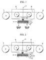
- FIG. 1 is a schematic diagram for illustrating a laser vapor deposition system using a conventional oxide target, wherein a symbol 1 denotes an oxide target, a symbol 2 denotes an Ag vapor-deposited film, a symbol 3 denotes an In soldering, a symbol 4 denotes a Cu-fixed plate, a symbol 5 denotes a SUS holder, a symbol 6 denotes a heater box, symbols 7 and 8 denote reels, a symbol 9 denotes a tape substrate, a symbol 10 denotes a plume, and a symbol 11 denotes a laser beam.
- a tape substrate 9 is disposed between the reels 7 and 8 in the heater box 6.
- the laser beam 11 is irradiated on the target 1 disposed under the heater box 6 to generate oxide fine particles from the surface of the oxide target 1 while the oxide target 1 is being moved in one direction.
- the fine particles are deposited on the surface of the substrate of the oxide target 1 to form an oxide film on the surface of the substrate.
- the structure of the oxide target 1 is such that the Cu-fixed plate 4, the In soldering 3, the Ag vapor-deposited film 2, and the oxide target 1 are bonded in this order onto the SUS holder 5, which can be cooled by circulating cooling water.
- the oxide target 1 described above there are problems in that the oxide target 1 is easily cleaved, and that cleavage or cracks easily occur due to the dramatic change in temperatures, or the like. Furthermore, since wettability of both materials with the oxide target 1 and the Ag vapor-deposited film 2 is poor, the oxide target 1 is peeled off from the body of the target, thereby leading to a problem in that film formation could not be stably carried out for a long period of time.
- the present invention has been made taking the above-described problems into consideration, and thus it is a preferred object thereof to provide an oxide target for laser vapor deposition and a method of manufacturing the same that is capable of stably carrying out film formation by extending the lifetime of a target in the oxide target used for the laser vapor deposition system.
- the present invention provides the following aspects:
- an Ag-soldering layer is bonded onto a fixed plate, an oxide-Ag mixed layer is bonded onto the Ag-soldering layer, and an oxide layer is bonded onto the oxide-Ag mixed layer.
- the oxide in the oxide-Ag mixed layer and the oxide layer are firmly sintered to each other.
- the oxide layer on the surface can be firmly fixed on the body of the target, thereby making it hard to peel off the oxide layer. As a result, a film structure can be stably maintained for a long period of time.
- the oxide target for laser vapor deposition of the present invention since Ag in the oxide-Ag mixed layer and the Ag-soldering layer has a heat resistance temperature as high as 900°C, it can be used without cooling a target even in laser vapor deposition with a film formation temperature as high as 800°C. As a result, the temperature distribution of the surface of the tape upon film formation can be kept good, thereby forming a high quality oxide film.
- FIG. 2 is a schematic diagram of a laser vapor deposition system provided with an oxide target for laser vapor deposition of a first embodiment of the present invention.
- a symbol 6 denotes a heater box
- symbols 7 and 8 denote reels
- a symbol 9 denotes a tape substrate
- a symbol 10 denotes a plume
- a symbol 11 denotes a laser beam
- a symbol 12 denotes an oxide target for laser vapor deposition
- a symbol 13 denotes an oxide layer
- a symbol 14 denotes an oxide-Ag mixed layer
- a symbol 15 denotes an Ag-soldering layer
- a symbol 16 denotes an Ni-based alloy fixed plate
- a symbol 17 denotes an SUS holder.
- the oxide target 12 for laser vapor deposition (hereinafter abbreviated as a target 12) of the present embodiment is an oxide target used for a laser vapor deposition system (not illustrated), in which a laser beam 11 is irradiated onto the target 12 to generate fine particles of an oxide from the surface of the target 12, and the fine particles are deposited on the surface of a substrate (not illustrated) to form an oxide film (not illustrated) on the surface of the substrate.
- the Ni-based alloy fixed plate 16 is fixed on the SUS holder 17, and the Ag-soldering layer 15 is bonded onto the Ni-based alloy fixed plate 16.
- the oxide-Ag mixed layer 14 is bonded onto the Ag-soldering layer 15, and the oxide layer 13 is bonded onto the oxide-Ag mixed layer 14.
- the oxides in the oxide layer 13 and the oxide-Ag mixed layer 14 are preferably of the same kinds of oxide materials.
- This oxide is an oxide material allowing film formation on the surface of a tape substrate 9, and can be selected from various oxide materials according to the purposes of film formation, and then used. Examples thereof include intermediate layer materials such as magnesium oxide and zirconium oxide, and oxide superconductive materials. Examples of these oxide superconductive materials include rare earth element-based oxide superconductors such as Y-Ba-Cu-O.
- the oxide-Ag mixed layer 14 is made by uniformly mixing the oxide powders and a predetermined amount of Ag powder, and then compression-molding these mixed materials into a plate shape with a desired thickness (a compressed-molded compact).
- the oxide-Ag mixed layer 14 is interposed between the Ag-soldering layer 15 of the target and the oxide layer 13, and the laminated layers of the oxide-Ag mixed layer 14, the Ag-soldering layer 15 and the oxide layer 13 are all heat-treated to a sintering temperature of the oxide to firmly sinter the oxide in the oxide-Ag mixed layer 14 and the oxide layer 13, as well as to metal-bond the Ag in the oxide-Ag mixed layer 14 to the Ag-soldering layer 15.
- the oxide layer 13 can be firmly fixed on the body of the target 12.
- Ag is uniformly dispersed in the oxide-Ag mixed layer 14.
- This oxide-Ag mixed layer 14 preferably has a thickness of 0.5 mm or more. Furthermore, the oxide-Ag-mixed layer 14 preferably has a ratio by volume of Ag in a range of from 5 to 20%.
- the oxide layer 13 is hard to be peeled off, and an endurance time of the bonded part of the target can be greatly increased. As a result, film structure can be stably maintained for a long period of time.
- the Ag-soldering layer 15 is bonded onto the Ni-based alloy fixed plate 16 on the body of the target, the oxide-Ag mixed layer 14 is bonded onto the Ag-soldering layer 15, and the oxide layer 13 is bonded onto the oxide-Ag mixed layer 14.
- the oxide-Ag mixed layer 14 and the oxide layer 13 are sintered and bonded to each other to firmly sinter the oxide in the oxide-Ag mixed layer 14 and the oxide layer 13, as well as to metal-bond the Ag in the oxide-Ag mixed layer 14 to the Ag-soldering layer 15.
- the oxide layer 13 of the surface can be firmly fixed on the body of the target thereby making the oxide layer 13 difficult to be peeled, and thus film structure can be stably maintained for a long period of time.
- the Ag in the oxide-Ag mixed layer 14 and the Ag-soldering layer 15 has a heat resistance temperature as high as 900°C, it can be used without cooling a target even in laser vapor deposition with a film formation temperature as high as 800°C. As a result, the distribution of temperatures of the surface of the tape substrate 9 upon film formation can be kept good, thereby forming a high quality oxide film.
- this oxide superconductive material was mixed with Ag powder at a ratio as described in "ratios (%) by volume of Ag/oxide” in Table 1, followed by compression-molding, and the thickness after final sintering was adjusted to give a thickness as described in "thickness of oxide-Ag mixed layer” in Table 1, to prepare various oxide-Ag mixed layers 14.
- the oxide layer 13 and the oxide-Ag bulk products were repeatedly put into a sintering furnace to sinter them at 900°C for 24 hours, and the sintered products were silver soldered onto the Ni-based alloy fixed plate 16.
- the oxide-Ag mixed layers having different thicknesses and ratios by volume of Ag were used as shown in FIG 2 to prepare an target 12, in which the SUS holder 17, the Ni-based alloy fixed plate 16, the Ag-soldering layer 15, the oxide-Ag mixed layer 14, and the oxide layer 13 were laminated in this order.
- the oxide in the oxide-Ag mixed layer 14 and the oxide layer 13 were firmly sintered to each other, as well as the Ag in the oxide-Ag mixed layer 14 being metal-bonded to the Ag-soldering layer 15, thereby firmly fixing the oxide layer 13 on the body of the target 12.
- the tape substrate 9 a tape was used in which an IBAD intermediate layer composed of Gd 2 Zr 2 O 7 had been formed on a surface of a tape substrate manufactured by Hastelloy according to an ion-beam-assisted vapor deposition (IBAD) method and a CeO 2 intermediate layer had been formed on a surface of the IBAD intermediate layer according to a pulse laser vapor deposition method.
- This tape substrate 9 was set between the reels 7 and 8, as shown in FIG. 2 , to pass through the inside of the heater box 6.
- the target 12 prepared as described above was attached on the bottom of the heater box 6, and a pulse laser beam from a pulse laser beam source (not shown) was irradiated to the oxide layer 13 of the target 12 while not cooling the SUS holder 17, and oxide fine particles were deposited on the surface of the tape substrate 9 moving in one direction to prepare an oxide superconductive tape.
- the temperature for film formation was 800°C.
- the limit of its use in terms of time is 100 hours.
- the target 12 (Sample No. 1-10) that had been prepared by using the oxide-Ag mixed layers having different thicknesses and ratios by volume of Ag was used to prepare an oxide superconductive tape, and cleavage or peeling of the target was caused to examine the time until film formation could not be stably carried out (which is hereinafter referred to as "endurance time of the bonded part of the target").
- the resulting oxide superconductive tape was cut into parts (length 500 mm) to measure a critical current density (Jc) of short wires at a liquid nitrogen temperature (which is hereinafter referred to as "short Jc"). The results thereof are summed up in Table 1.
- an oxide superconductive tape was prepared in the same manner as in Example, except that a comparative target (Sample No. 11 in Table 1) was used in which the Cu-fixed plate 4, the In soldering 3, the Ag vapor-deposited film 2, and the oxide target 1 composed of the oxide superconductive material were bonded in this order onto the SUS holder 5 which can be cooled by circulating cooling water, was prepared as shown in FIG. 1 .
- a comparative target (Sample No. 11 in Table 1) was used in which the Cu-fixed plate 4, the In soldering 3, the Ag vapor-deposited film 2, and the oxide target 1 composed of the oxide superconductive material were bonded in this order onto the SUS holder 5 which can be cooled by circulating cooling water, was prepared as shown in FIG. 1 .
- Table 1 Table 1 No.
- Ratio by volume of Agloxide (%) Thickness (mm) of oxide-Ag mixed layer Endurance time (h) of bonded part of target Short Jc (A/cm 2 ) 1 1 0.0 0 0 2 1 0.1 1 1.9 3 1 0.3 20 2.1 4 1 0.5 50 2.0 5 1 1.0 50 2.1 6 5 0.5 100 2.0 7 10 0.5 100 1.9 8 20 0.5 100 2.1 9 50 0.5 70 2.0 10 70 0.5 20 2.0 11 Comparative Example 20 1.5
- the endurance time of the bonded part of the target could be kept up to the life time of the target (100 hours).
- the ratio by volume of Ag/oxide exceeding 20%, the interface between the oxide layer 13 and the oxide-Ag mixed layer 14 was easily peeled off, and accordingly, there was a tendency of reduced endurance time.
Landscapes
- Chemical & Material Sciences (AREA)
- Chemical Kinetics & Catalysis (AREA)
- Engineering & Computer Science (AREA)
- Materials Engineering (AREA)
- Mechanical Engineering (AREA)
- Metallurgy (AREA)
- Organic Chemistry (AREA)
- Health & Medical Sciences (AREA)
- Toxicology (AREA)
- Superconductors And Manufacturing Methods Therefor (AREA)
- Physical Vapour Deposition (AREA)
- Superconductor Devices And Manufacturing Methods Thereof (AREA)
Applications Claiming Priority (1)
| Application Number | Priority Date | Filing Date | Title |
|---|---|---|---|
| JP2008046048A JP2009203511A (ja) | 2008-02-27 | 2008-02-27 | レーザー蒸着用酸化物ターゲット |
Publications (1)
| Publication Number | Publication Date |
|---|---|
| EP2098613A1 true EP2098613A1 (de) | 2009-09-09 |
Family
ID=40591829
Family Applications (1)
| Application Number | Title | Priority Date | Filing Date |
|---|---|---|---|
| EP09250509A Withdrawn EP2098613A1 (de) | 2008-02-27 | 2009-02-25 | Oxid-Target für Laserdampfabscheidung und Herstellungsverfahren dafür |
Country Status (3)
| Country | Link |
|---|---|
| US (1) | US8232232B2 (de) |
| EP (1) | EP2098613A1 (de) |
| JP (1) | JP2009203511A (de) |
Families Citing this family (2)
| Publication number | Priority date | Publication date | Assignee | Title |
|---|---|---|---|---|
| JP2013122065A (ja) * | 2011-12-09 | 2013-06-20 | Sumitomo Electric Ind Ltd | 機能性薄膜の成膜方法および成膜装置 |
| TWI463710B (zh) * | 2012-10-05 | 2014-12-01 | Subtron Technology Co Ltd | 接合導熱基板與金屬層的方法 |
Citations (4)
| Publication number | Priority date | Publication date | Assignee | Title |
|---|---|---|---|---|
| JPS5762518A (en) * | 1980-10-02 | 1982-04-15 | Nec Corp | Manufacture of oxide magnetic thin-film |
| JPS59232270A (ja) * | 1983-06-14 | 1984-12-27 | Matsushita Electric Ind Co Ltd | スパツタ−タ−ゲツト |
| JPS63270459A (ja) * | 1987-04-24 | 1988-11-08 | Matsushita Electric Ind Co Ltd | スパツタ用タ−ゲツトのボンデイング方法 |
| JPH062126A (ja) | 1992-06-18 | 1994-01-11 | Hitachi Ltd | スパッタリングターゲット材の接合方法 |
Family Cites Families (7)
| Publication number | Priority date | Publication date | Assignee | Title |
|---|---|---|---|---|
| JPH04202067A (ja) * | 1990-11-30 | 1992-07-22 | Hitachi Chem Co Ltd | 金属板と超電導セラミツクス用ターゲツトとの接合体及びその製造法並びに超電導薄膜の製造法 |
| US5431567A (en) * | 1993-05-17 | 1995-07-11 | Daftary; Fereidoun | Anatomical restoration dental implant system with interlockable various shaped healing cap assembly and matching abutment member |
| JP3829367B2 (ja) * | 1996-08-02 | 2006-10-04 | 東ソー株式会社 | スパッタリングターゲット |
| JP3880107B2 (ja) * | 1996-10-04 | 2007-02-14 | Dowaホールディングス株式会社 | スパッタリングターゲットとその接合方法 |
| JP4345054B2 (ja) * | 2003-10-09 | 2009-10-14 | 日立金属株式会社 | セラミックス基板用ろう材及びこれを用いたセラミックス回路基板、パワー半導体モジュール |
| JP2006233266A (ja) * | 2005-02-24 | 2006-09-07 | Fujikura Ltd | 薄膜形成装置 |
| US20080121521A1 (en) * | 2006-08-15 | 2008-05-29 | Chunghwa Picture Tubes, Ltd. | Plasma sputtering target assembly and manufacturing method therefor |
-
2008
- 2008-02-27 JP JP2008046048A patent/JP2009203511A/ja active Pending
-
2009
- 2009-02-25 EP EP09250509A patent/EP2098613A1/de not_active Withdrawn
- 2009-02-25 US US12/392,211 patent/US8232232B2/en active Active
Patent Citations (4)
| Publication number | Priority date | Publication date | Assignee | Title |
|---|---|---|---|---|
| JPS5762518A (en) * | 1980-10-02 | 1982-04-15 | Nec Corp | Manufacture of oxide magnetic thin-film |
| JPS59232270A (ja) * | 1983-06-14 | 1984-12-27 | Matsushita Electric Ind Co Ltd | スパツタ−タ−ゲツト |
| JPS63270459A (ja) * | 1987-04-24 | 1988-11-08 | Matsushita Electric Ind Co Ltd | スパツタ用タ−ゲツトのボンデイング方法 |
| JPH062126A (ja) | 1992-06-18 | 1994-01-11 | Hitachi Ltd | スパッタリングターゲット材の接合方法 |
Also Published As
| Publication number | Publication date |
|---|---|
| US8232232B2 (en) | 2012-07-31 |
| JP2009203511A (ja) | 2009-09-10 |
| US20090215630A1 (en) | 2009-08-27 |
Similar Documents
| Publication | Publication Date | Title |
|---|---|---|
| JP6399252B2 (ja) | 回路基板および窒化ケイ素焼結基板の製造方法 | |
| EP1452614B1 (de) | Gesinterter diamant mit hoher wärmeleitfähigkeit | |
| EP3566797B1 (de) | Metallpulver zur formung vom metalllaminat und unter verwendung dieses metallpulvers hergestellter formkörper | |
| AU758847B2 (en) | Alloy materials | |
| US5015618A (en) | Laser zone melted Bi--Sr--Ca--Cu--O thick films | |
| JP2001518564A (ja) | 超伝導体用基板 | |
| JP2001518681A (ja) | 耐酸化性の改善された基材 | |
| EP0202895B1 (de) | Verfahren zur Herstellung eines Verbundsupraleiters | |
| EP2818574A1 (de) | Sputtertarget und herstellungsverfahren dafür | |
| EP1592823B1 (de) | Verfahren zur herstellung eines zerstäubungstargets | |
| MX2008013921A (es) | Material de pelicula delgada superconductora y metodo para producir material de pelicula delgada superconductora. | |
| KR102403087B1 (ko) | 초전도 선재용 기판 및 그 제조 방법과 초전도 선재 | |
| JP2010132525A (ja) | 酸化層を有する窒化アルミニウム基板、窒化アルミニウム焼結体、それらの製造方法、回路基板、及びledモジュール | |
| EP2098613A1 (de) | Oxid-Target für Laserdampfabscheidung und Herstellungsverfahren dafür | |
| EP3904292A1 (de) | Supraleitender oxiddraht und verfahren zur herstellung davon | |
| JP2003529201A (ja) | 長寸の超伝導構造とその製造方法 | |
| JP7402120B2 (ja) | 酸化物超電導線材および酸化物超電導線材の製造方法 | |
| CN101313081A (zh) | 用于激光烧蚀的靶及其制造方法 | |
| JP2003323822A (ja) | 薄膜超電導線材およびその製造方法 | |
| EP4124184A1 (de) | Laminat, keramik-kupferleiterplatte, verfahren zur herstellung eines laminats und verfahren zur herstellung einer keramik-kupferleiterplatte | |
| JPH01275434A (ja) | 酸化物高温超電導膜の製造法 | |
| JPH02183915A (ja) | 酸化物超電導成形体 | |
| JP2001236834A (ja) | 酸化物超電導導体 | |
| JP2643972B2 (ja) | 酸化物系超電導材 | |
| JPH06235031A (ja) | Al−AlN系複合材料及びその製造方法 |
Legal Events
| Date | Code | Title | Description |
|---|---|---|---|
| PUAI | Public reference made under article 153(3) epc to a published international application that has entered the european phase |
Free format text: ORIGINAL CODE: 0009012 |
|
| AK | Designated contracting states |
Kind code of ref document: A1 Designated state(s): AT BE BG CH CY CZ DE DK EE ES FI FR GB GR HR HU IE IS IT LI LT LU LV MC MK MT NL NO PL PT RO SE SI SK TR |
|
| AX | Request for extension of the european patent |
Extension state: AL BA RS |
|
| 17P | Request for examination filed |
Effective date: 20100303 |
|
| AKX | Designation fees paid |
Designated state(s): DE FR |
|
| STAA | Information on the status of an ep patent application or granted ep patent |
Free format text: STATUS: THE APPLICATION HAS BEEN WITHDRAWN |
|
| 18W | Application withdrawn |
Effective date: 20130205 |