EP2097938B1 - Long lifetime phosphorescent organic light emitting device (oled) structures - Google Patents
Long lifetime phosphorescent organic light emitting device (oled) structures Download PDFInfo
- Publication number
- EP2097938B1 EP2097938B1 EP07875198.9A EP07875198A EP2097938B1 EP 2097938 B1 EP2097938 B1 EP 2097938B1 EP 07875198 A EP07875198 A EP 07875198A EP 2097938 B1 EP2097938 B1 EP 2097938B1
- Authority
- EP
- European Patent Office
- Prior art keywords
- organic layer
- emissive
- layer
- organic
- phosphorescent
- Prior art date
- Legal status (The legal status is an assumption and is not a legal conclusion. Google has not performed a legal analysis and makes no representation as to the accuracy of the status listed.)
- Active
Links
- 239000000463 material Substances 0.000 claims description 527
- 239000012044 organic layer Substances 0.000 claims description 384
- 239000010410 layer Substances 0.000 claims description 361
- 239000011368 organic material Substances 0.000 claims description 40
- UJOBWOGCFQCDNV-UHFFFAOYSA-N 9H-carbazole Chemical compound C1=CC=C2C3=CC=CC=C3NC2=C1 UJOBWOGCFQCDNV-UHFFFAOYSA-N 0.000 claims description 21
- 238000004770 highest occupied molecular orbital Methods 0.000 claims description 20
- IYYZUPMFVPLQIF-UHFFFAOYSA-N dibenzothiophene Chemical compound C1=CC=C2C3=CC=CC=C3SC2=C1 IYYZUPMFVPLQIF-UHFFFAOYSA-N 0.000 claims description 12
- 238000000295 emission spectrum Methods 0.000 claims description 9
- 125000005580 triphenylene group Chemical group 0.000 claims description 9
- SLGBZMMZGDRARJ-UHFFFAOYSA-N Triphenylene Natural products C1=CC=C2C3=CC=CC=C3C3=CC=CC=C3C2=C1 SLGBZMMZGDRARJ-UHFFFAOYSA-N 0.000 claims description 6
- 125000002524 organometallic group Chemical group 0.000 claims description 6
- 125000005259 triarylamine group Chemical group 0.000 claims description 3
- ODHXBMXNKOYIBV-UHFFFAOYSA-N triphenylamine Chemical compound C1=CC=CC=C1N(C=1C=CC=CC=1)C1=CC=CC=C1 ODHXBMXNKOYIBV-UHFFFAOYSA-N 0.000 claims description 3
- 150000001875 compounds Chemical class 0.000 description 128
- 235000019557 luminance Nutrition 0.000 description 59
- 230000000903 blocking effect Effects 0.000 description 50
- 229940126062 Compound A Drugs 0.000 description 49
- NLDMNSXOCDLTTB-UHFFFAOYSA-N Heterophylliin A Natural products O1C2COC(=O)C3=CC(O)=C(O)C(O)=C3C3=C(O)C(O)=C(O)C=C3C(=O)OC2C(OC(=O)C=2C=C(O)C(O)=C(O)C=2)C(O)C1OC(=O)C1=CC(O)=C(O)C(O)=C1 NLDMNSXOCDLTTB-UHFFFAOYSA-N 0.000 description 49
- 230000032258 transport Effects 0.000 description 47
- 230000037230 mobility Effects 0.000 description 30
- 239000002019 doping agent Substances 0.000 description 26
- 230000006798 recombination Effects 0.000 description 26
- 238000005215 recombination Methods 0.000 description 26
- 230000005525 hole transport Effects 0.000 description 23
- 238000002347 injection Methods 0.000 description 22
- 239000007924 injection Substances 0.000 description 22
- 230000007246 mechanism Effects 0.000 description 14
- 239000000758 substrate Substances 0.000 description 14
- 239000002800 charge carrier Substances 0.000 description 13
- 150000003384 small molecules Chemical class 0.000 description 13
- 238000000034 method Methods 0.000 description 10
- UFVXQDWNSAGPHN-UHFFFAOYSA-K bis[(2-methylquinolin-8-yl)oxy]-(4-phenylphenoxy)alumane Chemical compound [Al+3].C1=CC=C([O-])C2=NC(C)=CC=C21.C1=CC=C([O-])C2=NC(C)=CC=C21.C1=CC([O-])=CC=C1C1=CC=CC=C1 UFVXQDWNSAGPHN-UHFFFAOYSA-K 0.000 description 9
- -1 arylkyl Chemical group 0.000 description 8
- 230000008901 benefit Effects 0.000 description 8
- 238000000151 deposition Methods 0.000 description 7
- 238000004768 lowest unoccupied molecular orbital Methods 0.000 description 7
- 239000000243 solution Substances 0.000 description 7
- 238000012546 transfer Methods 0.000 description 7
- 238000004020 luminiscence type Methods 0.000 description 6
- 238000004519 manufacturing process Methods 0.000 description 6
- 239000011159 matrix material Substances 0.000 description 6
- 230000000052 comparative effect Effects 0.000 description 5
- 239000000412 dendrimer Substances 0.000 description 5
- 229920000736 dendritic polymer Polymers 0.000 description 5
- 230000005693 optoelectronics Effects 0.000 description 5
- 229920006395 saturated elastomer Polymers 0.000 description 5
- IJGRMHOSHXDMSA-UHFFFAOYSA-N Atomic nitrogen Chemical compound N#N IJGRMHOSHXDMSA-UHFFFAOYSA-N 0.000 description 4
- XCJYREBRNVKWGJ-UHFFFAOYSA-N copper(II) phthalocyanine Chemical compound [Cu+2].C12=CC=CC=C2C(N=C2[N-]C(C3=CC=CC=C32)=N2)=NC1=NC([C]1C=CC=CC1=1)=NC=1N=C1[C]3C=CC=CC3=C2[N-]1 XCJYREBRNVKWGJ-UHFFFAOYSA-N 0.000 description 4
- 230000002349 favourable effect Effects 0.000 description 4
- 238000005286 illumination Methods 0.000 description 4
- 238000005259 measurement Methods 0.000 description 4
- 125000001424 substituent group Chemical group 0.000 description 4
- 230000002411 adverse Effects 0.000 description 3
- 125000000217 alkyl group Chemical group 0.000 description 3
- 125000003118 aryl group Chemical group 0.000 description 3
- UEEXRMUCXBPYOV-UHFFFAOYSA-N iridium;2-phenylpyridine Chemical group [Ir].C1=CC=CC=C1C1=CC=CC=N1.C1=CC=CC=C1C1=CC=CC=N1.C1=CC=CC=C1C1=CC=CC=N1 UEEXRMUCXBPYOV-UHFFFAOYSA-N 0.000 description 3
- 230000000670 limiting effect Effects 0.000 description 3
- 229910052751 metal Inorganic materials 0.000 description 3
- 239000002184 metal Substances 0.000 description 3
- 239000000203 mixture Substances 0.000 description 3
- 229920000642 polymer Polymers 0.000 description 3
- LVTJOONKWUXEFR-FZRMHRINSA-N protoneodioscin Natural products O(C[C@@H](CC[C@]1(O)[C@H](C)[C@@H]2[C@]3(C)[C@H]([C@H]4[C@@H]([C@]5(C)C(=CC4)C[C@@H](O[C@@H]4[C@H](O[C@H]6[C@@H](O)[C@@H](O)[C@@H](O)[C@H](C)O6)[C@@H](O)[C@H](O[C@H]6[C@@H](O)[C@@H](O)[C@@H](O)[C@H](C)O6)[C@H](CO)O4)CC5)CC3)C[C@@H]2O1)C)[C@H]1[C@H](O)[C@H](O)[C@H](O)[C@@H](CO)O1 LVTJOONKWUXEFR-FZRMHRINSA-N 0.000 description 3
- 230000002829 reductive effect Effects 0.000 description 3
- GEQBRULPNIVQPP-UHFFFAOYSA-N 2-[3,5-bis(1-phenylbenzimidazol-2-yl)phenyl]-1-phenylbenzimidazole Chemical compound C1=CC=CC=C1N1C2=CC=CC=C2N=C1C1=CC(C=2N(C3=CC=CC=C3N=2)C=2C=CC=CC=2)=CC(C=2N(C3=CC=CC=C3N=2)C=2C=CC=CC=2)=C1 GEQBRULPNIVQPP-UHFFFAOYSA-N 0.000 description 2
- 230000015572 biosynthetic process Effects 0.000 description 2
- 238000004364 calculation method Methods 0.000 description 2
- 230000008859 change Effects 0.000 description 2
- 239000003086 colorant Substances 0.000 description 2
- JNGZXGGOCLZBFB-IVCQMTBJSA-N compound E Chemical compound N([C@@H](C)C(=O)N[C@@H]1C(N(C)C2=CC=CC=C2C(C=2C=CC=CC=2)=N1)=O)C(=O)CC1=CC(F)=CC(F)=C1 JNGZXGGOCLZBFB-IVCQMTBJSA-N 0.000 description 2
- 230000002596 correlated effect Effects 0.000 description 2
- 238000010168 coupling process Methods 0.000 description 2
- 238000005859 coupling reaction Methods 0.000 description 2
- 230000008021 deposition Effects 0.000 description 2
- 238000010586 diagram Methods 0.000 description 2
- 230000005281 excited state Effects 0.000 description 2
- 230000006872 improvement Effects 0.000 description 2
- 239000012535 impurity Substances 0.000 description 2
- 238000000025 interference lithography Methods 0.000 description 2
- 239000003446 ligand Substances 0.000 description 2
- 229910052757 nitrogen Inorganic materials 0.000 description 2
- 150000002894 organic compounds Chemical class 0.000 description 2
- 238000000059 patterning Methods 0.000 description 2
- 230000008569 process Effects 0.000 description 2
- 239000011241 protective layer Substances 0.000 description 2
- 238000010129 solution processing Methods 0.000 description 2
- 238000002207 thermal evaporation Methods 0.000 description 2
- DHDHJYNTEFLIHY-UHFFFAOYSA-N 4,7-diphenyl-1,10-phenanthroline Chemical group C1=CC=CC=C1C1=CC=NC2=C1C=CC1=C(C=3C=CC=CC=3)C=CN=C21 DHDHJYNTEFLIHY-UHFFFAOYSA-N 0.000 description 1
- DIVZFUBWFAOMCW-UHFFFAOYSA-N 4-n-(3-methylphenyl)-1-n,1-n-bis[4-(n-(3-methylphenyl)anilino)phenyl]-4-n-phenylbenzene-1,4-diamine Chemical group CC1=CC=CC(N(C=2C=CC=CC=2)C=2C=CC(=CC=2)N(C=2C=CC(=CC=2)N(C=2C=CC=CC=2)C=2C=C(C)C=CC=2)C=2C=CC(=CC=2)N(C=2C=CC=CC=2)C=2C=C(C)C=CC=2)=C1 DIVZFUBWFAOMCW-UHFFFAOYSA-N 0.000 description 1
- 101100394073 Caenorhabditis elegans hil-1 gene Proteins 0.000 description 1
- 101100506090 Caenorhabditis elegans hil-2 gene Proteins 0.000 description 1
- 238000004057 DFT-B3LYP calculation Methods 0.000 description 1
- 102100026816 DNA-dependent metalloprotease SPRTN Human genes 0.000 description 1
- 101710175461 DNA-dependent metalloprotease SPRTN Proteins 0.000 description 1
- YXLXNENXOJSQEI-UHFFFAOYSA-L Oxine-copper Chemical compound [Cu+2].C1=CN=C2C([O-])=CC=CC2=C1.C1=CN=C2C([O-])=CC=CC2=C1 YXLXNENXOJSQEI-UHFFFAOYSA-L 0.000 description 1
- 238000007792 addition Methods 0.000 description 1
- 125000003342 alkenyl group Chemical group 0.000 description 1
- 125000000304 alkynyl group Chemical group 0.000 description 1
- 230000000875 corresponding effect Effects 0.000 description 1
- 230000008878 coupling Effects 0.000 description 1
- 125000000753 cycloalkyl group Chemical group 0.000 description 1
- 238000013461 design Methods 0.000 description 1
- 238000005516 engineering process Methods 0.000 description 1
- 238000002474 experimental method Methods 0.000 description 1
- 229910052736 halogen Inorganic materials 0.000 description 1
- 125000001475 halogen functional group Chemical group 0.000 description 1
- 150000002367 halogens Chemical group 0.000 description 1
- 229910001385 heavy metal Inorganic materials 0.000 description 1
- 125000001072 heteroaryl group Chemical group 0.000 description 1
- 125000000623 heterocyclic group Chemical group 0.000 description 1
- 150000002484 inorganic compounds Chemical class 0.000 description 1
- 229910010272 inorganic material Inorganic materials 0.000 description 1
- 239000007788 liquid Substances 0.000 description 1
- 230000000873 masking effect Effects 0.000 description 1
- 230000000116 mitigating effect Effects 0.000 description 1
- 230000003287 optical effect Effects 0.000 description 1
- 238000013086 organic photovoltaic Methods 0.000 description 1
- 238000007639 printing Methods 0.000 description 1
- 238000004904 shortening Methods 0.000 description 1
- 230000011664 signaling Effects 0.000 description 1
- 239000002356 single layer Substances 0.000 description 1
- 241000894007 species Species 0.000 description 1
- 238000004611 spectroscopical analysis Methods 0.000 description 1
- 238000004528 spin coating Methods 0.000 description 1
- 230000007480 spreading Effects 0.000 description 1
- 238000003892 spreading Methods 0.000 description 1
- 239000000126 substance Substances 0.000 description 1
- 239000000725 suspension Substances 0.000 description 1
- TVIVIEFSHFOWTE-UHFFFAOYSA-K tri(quinolin-8-yloxy)alumane Chemical compound [Al+3].C1=CN=C2C([O-])=CC=CC2=C1.C1=CN=C2C([O-])=CC=CC2=C1.C1=CN=C2C([O-])=CC=CC2=C1 TVIVIEFSHFOWTE-UHFFFAOYSA-K 0.000 description 1
- 238000001947 vapour-phase growth Methods 0.000 description 1
- 239000003981 vehicle Substances 0.000 description 1
- 238000001429 visible spectrum Methods 0.000 description 1
- 230000005428 wave function Effects 0.000 description 1
- 238000003466 welding Methods 0.000 description 1
Images


Classifications
-
- H—ELECTRICITY
- H10—SEMICONDUCTOR DEVICES; ELECTRIC SOLID-STATE DEVICES NOT OTHERWISE PROVIDED FOR
- H10K—ORGANIC ELECTRIC SOLID-STATE DEVICES
- H10K50/00—Organic light-emitting devices
- H10K50/10—OLEDs or polymer light-emitting diodes [PLED]
- H10K50/11—OLEDs or polymer light-emitting diodes [PLED] characterised by the electroluminescent [EL] layers
- H10K50/125—OLEDs or polymer light-emitting diodes [PLED] characterised by the electroluminescent [EL] layers specially adapted for multicolour light emission, e.g. for emitting white light
- H10K50/13—OLEDs or polymer light-emitting diodes [PLED] characterised by the electroluminescent [EL] layers specially adapted for multicolour light emission, e.g. for emitting white light comprising stacked EL layers within one EL unit
-
- H—ELECTRICITY
- H10—SEMICONDUCTOR DEVICES; ELECTRIC SOLID-STATE DEVICES NOT OTHERWISE PROVIDED FOR
- H10K—ORGANIC ELECTRIC SOLID-STATE DEVICES
- H10K50/00—Organic light-emitting devices
- H10K50/10—OLEDs or polymer light-emitting diodes [PLED]
- H10K50/14—Carrier transporting layers
- H10K50/15—Hole transporting layers
- H10K50/155—Hole transporting layers comprising dopants
-
- H—ELECTRICITY
- H10—SEMICONDUCTOR DEVICES; ELECTRIC SOLID-STATE DEVICES NOT OTHERWISE PROVIDED FOR
- H10K—ORGANIC ELECTRIC SOLID-STATE DEVICES
- H10K50/00—Organic light-emitting devices
- H10K50/10—OLEDs or polymer light-emitting diodes [PLED]
- H10K50/17—Carrier injection layers
-
- H—ELECTRICITY
- H10—SEMICONDUCTOR DEVICES; ELECTRIC SOLID-STATE DEVICES NOT OTHERWISE PROVIDED FOR
- H10K—ORGANIC ELECTRIC SOLID-STATE DEVICES
- H10K85/00—Organic materials used in the body or electrodes of devices covered by this subclass
- H10K85/30—Coordination compounds
- H10K85/321—Metal complexes comprising a group IIIA element, e.g. Tris (8-hydroxyquinoline) gallium [Gaq3]
- H10K85/324—Metal complexes comprising a group IIIA element, e.g. Tris (8-hydroxyquinoline) gallium [Gaq3] comprising aluminium, e.g. Alq3
-
- H—ELECTRICITY
- H10—SEMICONDUCTOR DEVICES; ELECTRIC SOLID-STATE DEVICES NOT OTHERWISE PROVIDED FOR
- H10K—ORGANIC ELECTRIC SOLID-STATE DEVICES
- H10K85/00—Organic materials used in the body or electrodes of devices covered by this subclass
- H10K85/30—Coordination compounds
- H10K85/341—Transition metal complexes, e.g. Ru(II)polypyridine complexes
- H10K85/342—Transition metal complexes, e.g. Ru(II)polypyridine complexes comprising iridium
-
- H—ELECTRICITY
- H10—SEMICONDUCTOR DEVICES; ELECTRIC SOLID-STATE DEVICES NOT OTHERWISE PROVIDED FOR
- H10K—ORGANIC ELECTRIC SOLID-STATE DEVICES
- H10K85/00—Organic materials used in the body or electrodes of devices covered by this subclass
- H10K85/60—Organic compounds having low molecular weight
- H10K85/615—Polycyclic condensed aromatic hydrocarbons, e.g. anthracene
- H10K85/622—Polycyclic condensed aromatic hydrocarbons, e.g. anthracene containing four rings, e.g. pyrene
-
- H—ELECTRICITY
- H10—SEMICONDUCTOR DEVICES; ELECTRIC SOLID-STATE DEVICES NOT OTHERWISE PROVIDED FOR
- H10K—ORGANIC ELECTRIC SOLID-STATE DEVICES
- H10K85/00—Organic materials used in the body or electrodes of devices covered by this subclass
- H10K85/60—Organic compounds having low molecular weight
- H10K85/649—Aromatic compounds comprising a hetero atom
- H10K85/657—Polycyclic condensed heteroaromatic hydrocarbons
- H10K85/6572—Polycyclic condensed heteroaromatic hydrocarbons comprising only nitrogen in the heteroaromatic polycondensed ring system, e.g. phenanthroline or carbazole
-
- H—ELECTRICITY
- H10—SEMICONDUCTOR DEVICES; ELECTRIC SOLID-STATE DEVICES NOT OTHERWISE PROVIDED FOR
- H10K—ORGANIC ELECTRIC SOLID-STATE DEVICES
- H10K85/00—Organic materials used in the body or electrodes of devices covered by this subclass
- H10K85/731—Liquid crystalline materials
-
- H—ELECTRICITY
- H10—SEMICONDUCTOR DEVICES; ELECTRIC SOLID-STATE DEVICES NOT OTHERWISE PROVIDED FOR
- H10K—ORGANIC ELECTRIC SOLID-STATE DEVICES
- H10K2101/00—Properties of the organic materials covered by group H10K85/00
- H10K2101/10—Triplet emission
-
- H—ELECTRICITY
- H10—SEMICONDUCTOR DEVICES; ELECTRIC SOLID-STATE DEVICES NOT OTHERWISE PROVIDED FOR
- H10K—ORGANIC ELECTRIC SOLID-STATE DEVICES
- H10K2102/00—Constructional details relating to the organic devices covered by this subclass
- H10K2102/301—Details of OLEDs
- H10K2102/351—Thickness
Definitions
- the present invention relates to organic light emitting devices (OLEDs). More specifically, the present invention relates to OLEDs having particular structures that may enhance lifetime.
- Opto-electronic devices that make use of organic materials are becoming increasingly desirable for a number of reasons. Many of the materials used to make such devices are relatively inexpensive, so organic opto-electronic devices have the potential for cost advantages over inorganic devices. In addition, the inherent properties of organic materials, such as their flexibility, may make them well suited for particular applications such as fabrication on a flexible substrate. Examples of organic opto-electronic devices include organic light emitting devices (OLEDs), organic phototransistors, organic photovoltaic cells, and organic photodetectors. For OLEDs, the organic materials may have performance advantages over conventional materials. For example, the wavelength at which an organic emissive layer emits light may generally be readily tuned with appropriate dopants.
- OLEDs organic light emitting devices
- the wavelength at which an organic emissive layer emits light may generally be readily tuned with appropriate dopants.
- OLEDs make use of thin organic films that emit light when voltage is applied across the device. OLEDs are becoming an increasingly interesting technology for use in applications such as flat panel displays, illumination, and backlighting. Several OLED materials and configurations are described in U.S. Pat. Nos. 5,844,363 , 6,303,238 , and 5,707,745 .
- phosphorescent emissive molecules is a full color display.
- Industry standards for such a display call for pixels adapted to emit particular colors, referred to as "saturated" colors.
- these standards call for saturated red, green, and blue pixels. Color may be measured using CIE coordinates, which are well known to the art.
- a green emissive molecule is tris(2-phenylpyridine) iridium, denoted Ir(ppy) 3 , which has the structure of Formula I:
- organic includes polymeric materials as well as small molecule organic materials that may be used to fabricate organic opto-electronic devices.
- Small molecule refers to any organic material that is not a polymer, and "small molecules” may actually be quite large. Small molecules may include repeat units in some circumstances. For example, using a long chain alkyl group as a substituent does not remove a molecule from the "small molecule” class. Small molecules may also be incorporated into polymers, for example as a pendent group on a polymer backbone or as a part of the backbone. Small molecules may also serve as the core moiety of a dendrimer, which consists of a series of chemical shells built on the core moiety.
- the core moiety of a dendrimer may be a fluorescent or phosphorescent small molecule emitter.
- a dendrimer may be a "small molecule,” and it is believed that all dendrimers currently used in the field of OLEDs are small molecules.
- top means furthest away from the substrate, while “bottom” means closest to the substrate.
- first layer is described as “disposed over” a second layer, the first layer is disposed further away from substrate. There may be other layers between the first and second layer, unless it is specified that the first layer is "in contact with” the second layer.
- a cathode may be described as “disposed over” an anode, even though there are various organic layers in between.
- solution processible means capable of being dissolved, dispersed, or transported in and/or deposited from a liquid medium, either in solution or suspension form.
- a ligand is referred to as "photoactive" when it is believed that the ligand contributes to the photoactive properties of an emissive material.
- a first energy level (HOMO or LUMO) is considered “less than” or “lower” than a second energy level if it is lower on a conventional energy level diagram, which means that the first energy level would have a value that is more negative than the second energy level.
- a first energy level (HOMO or LUMO) is considered “higher” than a second energy level if it is higher on a conventional energy level diagram, which means that the first energy level would have a value that is less negative than the second energy level.
- the HOMO of CBP -5.32 eV and the HOMO of TPBI is -5.70 eV, therefore the HOMO of CBP is 0.38 eV "higher” than the HOMO of TPBI.
- the LUMO of mCP is -0.77 eV and the LUMO of CBP is -1.23 eV, therefore the LUMO of mCP is 0.46 eV "higher" than the LUMO of CBP.
- the above values were determined using density functional calculations performed using the Spartan 02 software package, available from Wavefunction Inc. of Irvine, Calif., at the B3LYP/6-31G* level. A pseudo potential option can be used for species containing heavy metals such as Ir(ppy) 3 . Density functional calculations have been demonstrated in the literature to be able to qualitatively predict energies of organic and inorganic compounds.
- the term "consisting essentially of' one or more materials as applied to a layer in an organic light emitting device” means that there may be materials present in addition to those listed, but any such additional materials are present only in minor quantities (such as impurities) and do not significantly affect the electronic properties or emissive of the device, i.e., they do not significantly contribute to the transport or trapping of holes or electrons, they do not result in a shift of the recombination location, and they do not significantly contribute to or participate in exciton decay, emissive or otherwise.
- EP1670082 US2005/0046337 , JP2005038672 , JP2003229272 , US2006/0232194 , US2005/0074630 disclose organic light emitting devices comprising phosphorescent light emitting layers with different phosphorescent material concentrations.
- an organic light emitting device with an interface in the emissive layer has an anode, a cathode, and an emissive layer disposed between the anode and the cathode.
- the emissive layer includes a first organic layer, which includes a first phosphorescent material and a first non-emissive material.
- the concentration of the first phosphorescent material in the first organic layer is 10 - 90 wt%
- the concentration of the first non-emissive material in the first organic layer is 10 - 90 wt%.
- the emissive layer also includes a second organic layer which includes a second phosphorescent material and a second non-emissive material.
- the concentration of the second phosphorescent material in the second layer is 3 - 25 wt%, and the concentration of the second non-emissive material in the second organic layer is 75-97 wt%.
- the concentration of the second phosphorescent material in the second organic layer is lower than the concentration of the first phosphorescent material in the first organic layer, preferably at least 5 wt% lower, and more preferably at least 10 wt% lower.
- the first non-emissive material and the second non-emissive material may be the same material or different materials, and the first phosphorescent material and the second phosphorescent material may be the same material or different materials.
- the first organic layer may consist essentially of the first phosphorescent material and the first non-emissive material
- the second organic layer may consist essentially of the first phosphorescent material and the first non-emissive material of the first organic layer.
- Device architectures that mitigate damage in the device and extend device lifetime are also provided for use with the first aspect, either individually or in combination.
- the first organic layer, the second organic layer, or both, may optionally further include a lower energy emissive material, wherein the concentration of the lower energy emissive material is 0.1-12 wt%.
- All organic layers between the first organic layer and the anode have a hole mobility and an electron mobility such that the hole mobility is at least twice as great as the electron mobility, preferably at least ten times greater, and more preferably at least 100 times greater.
- All organic layers between the first organic layer and the anode do not include any materials containing a group selected from the group consisting of triarylamine, napthyl, tri(N-carbazoyl)triphenylamine, tetraarylamine and carbazole.
- a fourth aspect not according to the invention, another architecture to mitigate damage is provided. There are no organic layers between the first organic layer and the anode.
- a third organic layer is provided, disposed between the first organic layer and the anode.
- the third organic layer consists essentially of the first phosphorescent material.
- the third organic layer is in direct contact with the first organic layer and the anode, such that it is the only layer between the first organic layer and the anode.
- the device includes no more than three different organic materials, minimizing the number of materials subject to damage.
- the device includes no more than four different organic materials, where one of the organic materials is an electron transport material present in the device only between the emissive layer and the cathode.
- one of the organic materials is an electron transport material present in the device only between the emissive layer and the cathode.
- the limitation on the number of materials minimizes the number of materials subject to damage.
- All organic layers between the first organic layer and the anode consist essentially of organometallic materials.
- All organic layers between the first organic layer and the anode have a hole conductivity sufficiently large such that an additional 10 nm thickness in the layer results in a voltage rise of 0.1 V or less at a current of 10 mA / cm 2 .
- the first non-emissive material has a triplet energy of 2.7 eV or greater.
- a lower energy emissive material may be used with the first aspect, with or without the various damage mitigation architectures.
- the lower energy emissive material may be a fluorescent emissive material, a phosphorescent material, or a combination of the two where there are multiple lower energy emissive materials.
- the concentration of the lower energy emissive material may be 0.1-12 wt%, and a lower energy emissive material may be present in only the first organic layer, only the second organic layer, or in both layers.
- An organic layer including a lower energy emissive material may consist essentially of a phosphorescent material, a non-emissive material, and a lower energy emissive material.
- a device similar to that of the first aspect is provided, but the concentration of the phosphorescent material in the second organic layer is higher than the concentration of the phosphorescent material in the first organic layer, as opposed to lower.
- the concentration of the first phosphorescent material in the first organic layer is 3 - 25 wt%, and the concentration of the first non-emissive material in the first organic layer is 75 - 97 wt%.
- the concentration of the phosphorescent material in the second layer is 10 - 90 wt%, and the concentration of the non-emissive material in the second organic layer is 10 - 90 wt%.
- the first organic layer may consist essentially of the first phosphorescent material and the first non-emissive material
- the second organic layer may consist essentially of the first phosphorescent material and the first non-emissive material of the first organic layer.
- the total thickness of the first and second organic layers is preferably at least 400 ⁇ .
- the thickness of the first organic layer is preferably at least 50 ⁇ and the thickness of the second organic layer is preferably at least 50 ⁇ .
- the first phosphorescent material preferably has a highest occupied molecular orbital that is at least 0.3 eV higher than the highest occupied molecular orbital of the first non-emissive material
- the second phosphorescent material preferably has a highest occupied molecular orbital that is at least 0.3 eV higher than the highest occupied molecular orbital of the first non-emissive material
- a fourth organic layer may be provided disposed between the second organic layer and the cathode.
- the fourth organic layer consists essentially of the second non-emissive material, and is in direct contact with the second organic layer.
- a fourth organic layer may be provided disposed between the second organic layer and the cathode.
- the fourth organic layer consists essentially of materials having a triplet energy at least 0.1 eV greater than the triplet energy of the second phosphorescent material, and the fourth organic layer is in direct contact with the second organic layer.
- the first non-emissive material may be selected from materials containing a group selected from the group consisting of triphenylene, carbazole, dibenzothiophene and dibenzothiophene coupled with carbazole.
- the first organic layer may be in direct contact with the second organic layer.
- an OLED comprises at least one organic layer disposed between and electrically connected to an anode and a cathode.
- the anode injects holes and the cathode injects electrons into the organic layer(s).
- the injected holes and electrons each migrate toward the oppositely charged electrode.
- an "exciton” which is a localized electron-hole pair having an excited energy state, is formed.
- Light is emitted when the exciton relaxes via a photoemissive mechanism.
- the exciton may be localized on an excimer or an exciplex. Non-radiative mechanisms, such as thermal relaxation, may also occur, but are generally considered undesirable.
- the initial OLEDs used emissive molecules that emitted light from their singlet states ("fluorescence") as disclosed, for example, in U.S. Pat. No. 4,769,292 . Fluorescent emission generally occurs in a time frame of less than 10 nanoseconds.
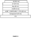
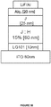
- FIG. 1 shows an organic light emitting device 100.
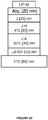
- Device 100 may include a substrate 110, an anode 115, a hole injection layer 120, a hole transport layer 125, an electron blocking layer 130, an emissive layer 135, a hole blocking layer 140, an electron transport layer 145, an electron injection layer 150, a protective layer 155, and a cathode 160.
- Cathode 160 is a compound cathode having a first conductive layer 162 and a second conductive layer 164.
- Device 100 may be fabricated by depositing the layers described, in order. The properties and functions of these various layers, as well as example materials, are described in more detail in US 7,279,704 at cols. 6-10.
- a flexible and transparent substrate-anode combination is disclosed in U.S. Pat. No. 5,844,363 .
- An example of a p-doped hole transport layer is m-MTDATA doped with F.sub.4-TCNQ at a molar ratio of 50:1, as disclosed in U.S. Patent Application Publication No. 2003/0230980 .
- Examples of emissive and host materials are disclosed in U.S. Pat. No. 6,303,238 to Thompson et al.
- An example of an n-doped electron transport layer is BPhen doped with Li at a molar ratio of 1:1, as disclosed in U.S. Patent Application Publication No.
- FIG. 2 shows an inverted OLED 200.
- the device includes a substrate 210, a cathode 215, an emissive layer 220, a hole transport layer 225, and an anode 230.
- Device 200 may be fabricated by depositing the layers described, in order. Because the most common OLED configuration has a cathode disposed over the anode, and device 200 has cathode 215 disposed under anode 230, device 200 may be referred to as an "inverted" OLED. Materials similar to those described with respect to device 100 may be used in the corresponding layers of device 200.
- FIG. 2 provides one example of how some layers may be omitted from the structure of device 100.
- FIGS. 1 and 2 The simple layered structure illustrated in FIGS. 1 and 2 is provided by way of nonlimiting example, and it is understood that embodiments of the invention may be used in connection with a wide variety of other structures.
- the specific materials and structures described are exemplary in nature, and other materials and structures may be used.
- Functional OLEDs may be achieved by combining the various layers described in different ways, or layers may be omitted entirely, based on design, performance, and cost factors. Other layers not specifically described may also be included. Materials other than those specifically described may be used. Although many of the examples provided herein describe various layers as comprising a single material, it is understood that combinations of materials, such as a mixture of host and dopant, or more generally a mixture, may be used. Also, the layers may have various sublayers.
- hole transport layer 225 transports holes and injects holes into emissive layer 220, and may be described as a hole transport layer or a hole injection layer.
- an OLED may be described as having an "organic layer" disposed between a cathode and an anode. This organic layer may comprise a single layer, or may further comprise multiple layers of different organic materials as described, for example, with respect to FIGS. 1 and 2 .
- OLEDs comprised of polymeric materials (PLEDs) such as disclosed in U.S. Pat. No. 5,247,190 to Friend et al.
- PLEDs polymeric materials
- OLEDs having a single organic layer may be used.
- OLEDs may be stacked, for example as described in U.S. Pat. No. 5,707,745 to Forrest et al.
- the OLED structure may deviate from the simple layered structure illustrated in FIGS. 1 and 2 .
- the substrate may include an angled reflective surface to improve out-coupling, such as a mesa structure as described in U.S. Pat. No. 6,091,195 to Forrest et al. , and/or a pit structure as described in U.S. Pat. No. 5,834,893 to Bulovic et al.
- any of the layers of the various embodiments may be deposited by any suitable method.
- preferred methods include thermal evaporation, ink-jet, such as described in U.S. Pat. Nos. 6,013,982 and 6,087,196 , organic vapor phase deposition (OVPD), such as described in U.S. Pat. No. 6,337,102 to Forrest et al , and deposition by organic vapor jet printing (OVJP), such as described in U.S. patent application Ser. No. 10/233,470 .
- OVPD organic vapor phase deposition
- OJP organic vapor jet printing
- Other suitable deposition methods include spin coating and other solution based processes. Solution based processes are preferably carried out in nitrogen or an inert atmosphere.
- preferred methods include thermal evaporation.
- Preferred patterning methods include deposition through a mask, cold welding such as described in U.S. Pat. Nos. 6,294,398 and 6,468,819 , and patterning associated with some of the deposition methods such as ink-jet and OVJD. Other methods may also be used.
- the materials to be deposited may be modified to make them compatible with a particular deposition method.
- substituents such as alkyl and aryl groups, branched or unbranched, and preferably containing at least 3 carbons, may be used in small molecules to enhance their ability to undergo solution processing. Substituents having 20 carbons or more may be used, and 3-20 carbons is a preferred range. Materials with asymmetric structures may have better solution processibility than those having symmetric structures, because asymmetric materials may have a lower tendency to recrystallize. Dendrimer substituents may be used to enhance the ability of small molecules to undergo solution processing.
- Devices fabricated in accordance with embodiments of the invention may be incorporated into a wide variety of consumer products, including flat panel displays, computer monitors, televisions, billboards, lights for interior or exterior illumination and/or signaling, heads up displays, fully transparent displays, flexible displays, laser printers, telephones, cell phones, personal digital assistants (PDAs), laptop computers, digital cameras, camcorders, viewfinders, micro-displays, vehicles, a large area wall, theater or stadium screen, or a sign.
- PDAs personal digital assistants
- Various control mechanisms may be used to control devices fabricated in accordance with the present invention, including passive matrix and active matrix. Many of the devices are intended for use in a temperature range comfortable to humans, such as 18 degrees C. to 30 degrees C., and more preferably at room temperature (20-25 degrees C.).
- the materials and structures described herein may have applications in devices other than OLEDs.
- other optoelectronic devices such as organic solar cells and organic photodetectors may employ the materials and structures.
- organic devices such as organic transistors, may employ the materials and structures.
- halo, halogen, alkyl, cycloalkyl, alkenyl, alkynyl, arylkyl, heterocyclic group, aryl, aromatic group, and heteroaryl are known to the art, and are defined in US 7,279,704 at cols. 31-32.
- FIG. 8 shows a general phosphorescent OLED structure.
- a new architecture for a phosphorescent OLED is disclosed.
- FIG. 9 shows a simplified device architecture that incorporates a thick emissive layer (EML) between a hole injection layer (HIL) and a blocking layer (BL). It is demonstrated that when the NPD HTL is replaced with a COMPOUND B:COMPOUND A doped layer in a phosphorescent OLED, this leads to extremely long lifetime of a new green phosphorescent OLED.
- EML thick emissive layer
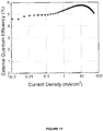
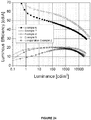
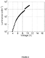
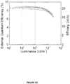
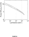
- COMPOUND B:COMPOUND A A green device has been demonstrated with 600 ⁇ COMPOUND B:COMPOUND A 15% EML with an efficiency of 44 cd/A and an 80% lifetime of 65,000h at 1000 cd/m 2 (nits), see Table 2, compare Example 1 to Comparative Example 2.
- the 600 ⁇ COMPOUND B:COMPOUND A layer provides both electron and hole transport capabilities.
- COMPOUND B provides very stable matrix.
- COMPOUND A is provided as a hole-transporting dopant, because COMPOUND B has preferential electron transporting characteristics.
- the doped COMPOUND B:COMPOUND A layer can also be used as the HTL for red and blue structures.
- COMPOUND B:COMPOUND A is an example to demonstrate the concept of a doped HTL.
- COMPOUND A can also be used as a hole injection layer, and COMPOUND B can function as a layer between the emissive layer and the electron transport layer (if present) and subsequent cathode.
- Some features disclosed herein enable a significant improvement in phosphorescent OLED stability. This includes the utilization of a material (COMPOUND B), which was originally designed to be a host and has now been demonstrated to be an effective BL (blocking layer) and HTL (Hole transport layer).
- COMPONENT B a material
- HTL Hole transport layer
- CBP host HPT blocking layer (BL) and NPD hole transporter layer (HTL) materials presents significant impediments to the realization of a stable and long-lived green phosphorescent OLED.
- the replacement of a NPD HTL with a layer of COMPOUND B doped with COMPOUND A for green devices dramatically improves device lifetime.
- the concept is also applicable to blue devices.
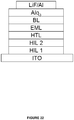
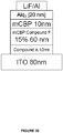
- Compound B is a very stable host material. Green structure and performance with Compound B used in various layers within a device as a host, blocking layer and component of the hole-transporting layer is disclosed. Table 1 shows device data on improving green Phosphorescent OLED stability. FIG. 8 shows a general device structure showing the structure of the layers from Table 1.
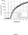
- Table 1 Evolution of green phosphorescent OLED performance due to new materials in device structure Structure 1 2 3 4 5 6 HIL 100 ⁇ Compound A Compound A Compound A Compound A Compound A Compound A Compound A CuPc HTL 300 ⁇ NPD NPD NPD Compound B: Compound A 15% Compound B: Compound A 30% Compound B: Compound A 15% EML 300 ⁇ CBP: Compound A 10% Compound B: Compound A 10% Compound B: Compound A 15% Compound B: Compound A 15% Compound B: Compound A 15% Compound B: Compound A 15% Compound B: Compound A 15% Compound B: Compound A 15% Compound B: Compound A 15% BL HPT 50 ⁇ HPT 50 ⁇ Compound B 100 ⁇ Compound B 100 ⁇ Compound B 100 ⁇ Compound B 100 ⁇ Compound B 100 ⁇ ETL Alq 450 ⁇ Alq 450 ⁇ Alq 400 ⁇ Alq 400 ⁇ Alq 400 ⁇ Voltage at 1000 nits [V] 5.8 5.7 6.4 7.6 6.4 8.8 Luminous efficiency at 1000 nits [
- COMPOUND B transports electrons
- COMPOUND A dopant transports holes in the layers including both COMPOUND A and COMPOUND B.
- Replacement of NPD makes the lifetime of green devices similar to those of red devices (> 100,000h).
- the same concept of a doped HTL can be used utilizing other materials and can be applied to red and blue Phosphorescent OLEDs.
- HIL is 100% the p-type dopant e.g. COMPOUND A and then a host material is introduced, e.g., COMPOUND B as one looks further from the anode.
- a host material e.g., COMPOUND B as one looks further from the anode.
- Multiple layers of differing concentrations (0-100%) of dopant and host can also be employed between the anode and BL or ETL.
- COMPOUND B may also be used as the host for red and blue-green emitters.
- COMPOUND B may also be used as the BL in red green, blue, or white devices or any other color.
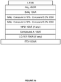
- FIG. 21 provides the structure for the devices described in Table 2.
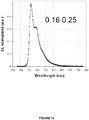
- Table 2 Device performance comparison when NPD HTL is replaced in device Parameters Example 1 Example 2 Example 3 Example 4 Example 5 Comparative Example HIL 100 ⁇ Compound A CuPc none Compound A Compound A Compound A HTL 300 ⁇ Compound B: Compound A 15% Compound B: Compound A 15% Compound B: Compound A 30% Compound B: Compound A 15% NPD EML 300 ⁇ Compound B: Compound A 15% Compound B: Compound A 15% Compound B: Compound A 15% Compound B: Compound A 15% Compound B: Compound A 15% Compound B: Compound A 15% Compound B: Compound A 15% Compound B: Compound A 15% CBP: Compound A 10% Compound B: Compound A 15% CIE [x,y] 0.38 0.59 0.36 0.61 0.36 0.60 0.37 0.60 0.60 0.38 0.59 Voltage at 1000 nits [v] 7.6 8.8 8.6 6.4 7.8 6.4 Luminous efficiency at 1000 nits [Cd/Al 44.2
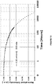
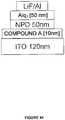
- Example 5 A superior performance, and the best performance for the devices measured in the particular experiment shown in Table 1, which is long lifetime in combination with high device efficiency and low operating voltage, is Example 5 from Table 1.
- the structure of Example 5 is shown in FIG. 9 .
- This device has only three organic materials.
- HIL, EML and BL of this device can be considered as a Compound A: Compound B layer with graded concentrations from 100% of compound A next to ITO (hole injection interface) and 100% of compound B next to Alq ETL (electron injection interface).
- Tables 1 and 2 illustrate several points that are associated with superior device performance.
- device architectures having the following favorable architecture, which may be used alone or in combination: Utilization of stable hosts, such as triphenylene compounds, for example Compound B
- Devices may be fabricated using a stable host material that is a triphenylene compound or a carbazole compound.
- the devices may include only 3 or only 2 organic components, and may include layers having different concentrations of the same materials. Table 3 shows examples of such devices.
- the structure for the devices of Table 3 is shown in FIG. 8 .
- the designations in FIG. 8 regarding HTL and ETL are somewhat flexible, in that both of these layers are believed to emit in many of the structures, particularly those where the HTL and ETL have the same materials but in different concentrations.
- Devices 1 and 2 of Table 3 were actually fabricated, while devices 3 and 4 were not but are included for illustrative purposes. It is believed that Compound S is an example of a phosphorescent molecule that may transport electrons in an emissive layer.
- the devices have application in flat panel displays and in lighting applications.
- the superior devices demonstrated have the advantage of enabling longer lifetime in high efficiency phosphorescent OLEDs.
- No special fabrication equipment is necessary, and devices may be fabricated by methods known in the art. Shadow masking may be a consideration depending on whether common layers can be employed in the case of side by side RGB applications.
- FIG. 3 shows an organic light emitting device having first and second organic layers with different concentrations of phosphorescent material and non-emissive materials, and organic layers between the first organic layer and the anode with specific charge carrier mobility characteristics.
- the device of FIG. 3 includes a substrate 310, an anode 315, a third organic layer 320, an emissive layer having a first organic layer 330 and a second organic layer 340, a hole blocking layer 350, an electron transport layer 360, and a cathode 370. Hole blocking layer 350 and electron transport layer 360 are optional.
- the device of FIG. 3 and various other devices shown herein, is shown with the anode adjacent to the substrate, as is common for many devices, but the devices could also have the cathode adjacent to the substrate.
- First organic layer 330 is disposed between the anode and the cathode, and includes a phosphorescent material and a non-emissive material.
- concentration of the phosphorescent material in the first organic layer is 10 - 90 wt%.
- concentration of the non-emissive material in the first organic layer is 10 - 90 wt%.
- Second organic layer 340 is disposed between the first organic layer and the cathode. Second organic layer 340 is preferably in direct contact with first organic layer 330, but there may also be a thin organic layer in between first and second organic layers 330 and 340 that is capable of transporting both electrons and holes. Second organic layer also include a phosphorescent material and a non-emissive material.
- first and second organic layers 330 and 340 include only the phosphorescent material and the non-emissive material. This is favorable because minimizing the number of materials simplifies fabrication, and avoids failure mechanisms that may be associated with additional materials.
- FIG. 3 shows organic layers that include a "phosphorescent” material and a “non-emissive” material.
- the "phosphorescent" material is a material capable of emitting light from a triplet excited state at room temperature, for example, at about 18- 25 degrees C.
- any given phosphorescent material may or may not emit light in a particular layer or in a particular device.
- the phosphorescent material does emit light.
- the phosphorescent material does not emit light, but rather transfers excitons to other molecules, which may be phosphorescent or fluorescent, which then emit light.
- the phosphorescent nature of the material still plays a role in these devices, because the ability to emit light from a triplet excited state at room temperature is correlated with other properties, such as intersystem crossing and strong spin orbit coupling, which allow triplets to efficiently form on the molecule and transfer to other molecules, even though it may not emit light.
- many phosphorescent materials are also good hole transporters.
- the definition of the term " phosphorescent" as defined this application is believed to be generally consistent with its use in the art, but is not intended to extend to other applications where the term may be used in a different manner.
- the "non-emissive" material does not emit light in the device for which the material is described as “non-emissive.”
- the non-emissive material is not necessarily electrically inert in the device, and may often be involved with charge transport, most often electron transport.
- the material may be emissive in other contexts, for example in solution or in other devices.
- solid-state considerations in the particular device make it such that the material does not emit light in the device.
- the "non-emissive" material may be doped with a phosphorescent material having a triplet energy that is at least 0.1 eV lower than that of the non-emissive material, such that any triplets that do form on the non-emissive material transfer to the phosphorescent material rather than emit light.
- the phosphorescent material is responsible for the transport of holes in the emissive layer, and that a non-emissive host material is responsible for the transport of electrons. It is believed that the change in concentration of phosphorescent material between first organic layer 330 and second organic layer 340 may cause the mobility of electrons to be higher in first organic layer 330 than in second organic layer 340, and the mobility of holes to be higher in second organic layer 340 than in first organic layer 330. As a result, recombination of electrons and holes may occur at or near the interface between first organic layer 330 and second organic layer 340.
- the concentration of phosphorescent material in second organic layer 340 is preferably at least 5 wt% lower than the concentration in first organic layer 330, and is more preferably at least 10 wt% lower. Together, first organic layer 330 and second organic layer 340 may form the emissive layer of the device. Because recombination occurs at or near an interface between first and second organic layers 330 and 340, i.e., at an interface within the emissive layer, issues caused by recombination near interfaces with a non-emissive layer may be avoided. The reasoning described in these paragraph applies to various devices described herein that have an emissive layer with an internal interface, i.e., an interface between the first and second organic layers.
- the phosphorescent material of first organic layer 330 and second organic layer 340 may be the same material, or may be different phosphorescent materials.
- the non-emissive material of first organic layer 330 and second organic layer 340 may be the same material, or different materials.
- first organic layer 330 and second organic layer 340 simplifies fabrication by reducing the number of materials in the device.
- each new material may introduce new failure mechanisms
- using the same material in multiple layers may reduce failure mechanisms.
- Using the same non-emissive material may also assist in spreading out the recombination zone for the device, which is also helpful to achieving higher device lifetime, while still allowing recombination to occur near an interface between first organic layer 330 and second organic layer 340 by adjusting the concentration of non-emissive materials at the interface.
- first organic layer 330 and second organic layer 340 also has advantages. Different materials may have different charge transport properties. Where the non-emissive materials are predominantly responsible for the transport of a particular charge carrier, most often electrons, using different non-emissive materials in first organic layer 330 and second organic layer 340 may make it easier to control where recombination occurs in the device. Specifically, by choosing different non-emissive materials for first organic layer 330 and second organic layer 340, it may be easier to create a gradient of charge carriers near an interface between first organic layer 330 and second organic layer 340, because the difference in non-emissive materials may be used for this purpose in addition to the concentration of non-emissive materials.
- first organic layer 330 and second organic layer 340 Using the same phosphorescent material in both first organic layer 330 and second organic layer 340, but at different concentrations, has many of the same advantages as described above with respect to use of the same non-emissive material. Fewer materials may mean fewer failure mechanisms. The different concentrations may allow recombination to be controlled to occur near an interface between first organic layer 330 and second organic layer 340, while the use of the same phosphorescent material allows the recombination zone to be relatively broad.
- first organic layer 330 and second organic layer 340 Using different phosphorescent materials in both first organic layer 330 and second organic layer 340, at different concentrations, has many of the same advantages as described above with respect to the use of different non-emissive materials.
- the use of different materials may add an extra parameter that may be used to control where recombination occurs.
- the phosphorescent materials may or may not emit light in the device. Where highly efficient saturated emission is desired, perhaps for use in a display device that requires saturated emission, it may be preferable to use the same phosphorescent material in both first organic layer 330 and second organic layer 340 as the emissive material. In a configuration where the phosphorescent material(s) transports charge but do not emit, an additional material, described as an "lower energy" material, may be added to first organic layer 330 and second organic layer 340, and emit light.
- “lower energy” it is meant that the peak of the emission spectra of the lower energy emissive material is at least 20 nm higher than the peak of the emission spectra of the phosphorescent material in the same layer.
- Excitons may be present on the lower energy emissive material through a variety of mechanisms, and the way in which excitons reach the lower energy emissive material is not intended to be limiting. For example, excitons may form on the phosphorescent material and transfer to the lower energy emissive material, or excitons may form directly on the lower energy emissive material.
- the lower energy emissive material may be a fluorescent material that accepts excitons from the phosphorescent material, including excitons that form as triplets on the phosphorescent material.
- first and second organic layers 330 and 340 may be used in first and second organic layers 330 and 340 as the emitters in those layers, such that there are multiple emissive materials in the device.
- An additional material or materials, described as "lower energy” materials, may also be added to one or both of first and second organic layers 330 and 340.
- different lower energy emissive materials may be used in both first and second organic layers 330 and 340, or a lower energy emissive material may be used in one of the first and second organic layers 330 and 340 while the phosphorescent material emits from the other of the first and second organic layers 330 and 340.
- devices having emissive layers with a first and second organic layer having an interface between them may still be subject to short lifetimes. It is believed that a leading failure mechanism in many phosphorescent organic light emitting devices involves electrons passing from the cathode, through the emissive layer, to organic layers on the anode side of the emissive layer. It is believed that many organic materials that are used on the anode side of OLEDs are vulnerable to damage from such electrons.
- FIGS. 44 - 50 and the associated text show the role of a common hole transport material, NPD, in shortening device lifetime.
- the use of an emissive layer having first and second organic layers 330 and 340 favorably allows recombination to occur at an interface within the emissive layer.
- the number of excitons that reach a non-emissive layer, and the number of charge carriers that cross the entire emissive layer to reach the other side may be reduced.
- third organic layer 320 is on the anode side of the emissive layer, i.e., first and / or second organic layers 330 and 340. There may be more than one organic layer in the position occupied by third organic layer 320.
- Each organic layer between the emissive layer and the anode may include a single organic material, or multiple organic materials.
- the material of each layer has a hole mobility that is significantly higher than the electron mobility of that layer.
- the hole mobility of the layer is significantly higher than the electron mobility of the layer.
- the hole mobility of a "layer” is strongly correlated with the hole mobility of the material in that layer that is predominantly responsible for transporting holes in the layer, particularly where the material in question is present in significant quantities. Electron and hole mobilities may be measured by various methods, including time of flight, dark current injection, and admittance spectroscopy. By significantly higher, it is meant that the hole mobility is at least twice the electron mobility, preferably at least ten times as great as the electron mobility, and most preferably at least 100 times as great as the electron mobility.
- NPD is traditionally used a hole transport layer (HTL) and it is often in contact with the EML.
- HTL hole transport layer
- This suggests that electrons may easily be transported by NPD in conventional structures. This enables two potentially unfavorable situations. Firstly, electrons and holes may recombine in NPD.
- NPD may be a stable hole transport layer but devices that exhibit NPD emission are not expected to be operationally stable because the emission is inefficient and NPD was not included in the device for this purpose.
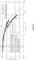
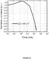
- a device with NPD and BAlq emissions is shown in FIG 38 .
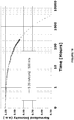
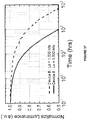
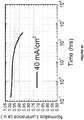
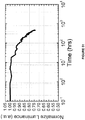
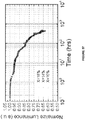
- the lifetime (LT50) of this device, shown in FIG. 43 is less than 300 hrs when the device is drive at a constant current of 20 mA/cm 2 .
- a similar device with only Alq emission has a much longer life time.
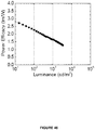
- the luminance of the Alq emitting device drops to about 86% (see FIG. 49 ) of its initial value after 300 hrs and for a continuous drive current of 40 mA/cm 2 .
- NPD may be intrinsically unstable to electrons. There is ample evidence to believe that NPD is stable in hole only devices; however, its stability to electrons is not established.
- third organic layer 320 is a single organic layer disposed between first organic layer 330 and anode 315, i.e., third organic layer 320 is in direct contact with first organic layer 330 and anode 315. Also in this preferred aspect, third organic layer 320 includes only the phosphorescent material of first organic layer 330. In general, electrons are present in the emissive layer of a device, and the emissive material of a device is exposed to electrons in the emissive layer. As a result, most phosphorescent emissive molecules that are used in devices having reasonably long lifetimes are resistant to damage from electrons.
- first and second organic layers 330 and 340 in an additional role, as the only organic material between first organic layer 330 and anode 315, i.e. as a hole transport molecule, may result in a device that avoids failure mechanisms associated with electron damage to organic layers on the anode side of the emissive layer.
- Another way to avoid damage and shorter lifetimes caused by electrons damaging organic materials on the anode side of the emissive layer is to avoid using classes of materials on the anode side of the emissive layer that are susceptible to damage from electrons. It is believed that many materials commonly used on the anode side of the emissive layer are susceptible to such damage. NPD is one example of such materials.
- materials that are avoided on the anode side of the emissive layer include molecules having a group from the following list: triarylamine, napthyl, tri(N-carbazoyl)triphenylamine, tetraarylamine and carbazole.
- Another way to avoid damage and shorter lifetimes caused by electrons damaging organic materials on the anode side of the emissive layer is to use materials on the anode side of the emissive layer having a high hole conductivity.
- a high hole conductivity may allow holes to be injected into the emissive layer at a rate sufficient to minimize the number of electrons reaching the anode side of the emissive layer.
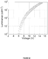
- a useful measure of the conductivity of a layer is the voltage rise caused in a device by making a particular layer thicker. Specifically, several otherwise identical devices may be fabricated, except for one difference -- the devices have a particular layer for which conductivity is being measured that has different thicknesses in different devices.
- the voltage difference caused by an increase in the thickness of a particular layer may be isolated from the voltage difference due to various interfaces and layers other than the one for which conductivity is being measured.
- Hole conductivity specifically may be measured by performing such a measurement in a device where the layer of varying thickness is located in the device at a location where, based on the other layers in the device, electrons do not reach in large quantities and holes are the predominant charge carrier.
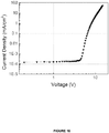
- Parameters such as carrier mobility that affect conductivity may be a function of current, although it is believed that the dependence is mild. To control for this factor, the measurements may be performed at a particular current density. 10 mA / cm 2 is a suitable current density that was used for the measurements described herein.
- the hole conductivity of NPD has been measured in this way, and it was demonstrated that the voltage across the device at a current of 10 mA / cm 2 increases by 0.6 V for each additional 10 nm of NPD thickness.
- the hole conductivity of LG101TM (available from LG, Korea) was measured in a similar way, and it was demonstrated that the voltage across the device at a current of 10 mA / cm 2 increases by less than 0.5 V for each additional 10 nm of LG101 thickness.
- a device having between the emissive layer and the anode only layers for which the voltage across the device rises by 0.1 V or less per additional 10 nm of layer thickness may favorably minimize damage to organic layers on the anode side of the emissive layer.
- a layer of LG101 is one example of such a layer.
- organometallic materials are generally more resistant to damage from electrons than certain materials commonly used in hole transport layers, such as NPD. Indeed, organometallic materials used as emitters are exposed to an environment relatively rich in electrons in the emissive layer(s) of a device. Using such materials in the relatively electron poor anode side of the device should not result in significant electron damage.
- organometallic materials used as emitters in organic light emitting devices are good hole transporters, and are believed in many cases to be responsible for hole transport in the emissive layers of an organic light emitting device.
- Another way to avoid damage and shorter lifetimes caused by electrons damaging organic materials on the anode side of the emissive layer is to use a high triplet energy material for the first non-emissive material (i.e. the non-emissive material of the first organic layer), such as first organic layer 330. It is believed one damage mechanism that reduces device lifetime may involve triplets reaching the anode side of the emissive layer, and damaging organic materials on the anode side of the emissive layer. In a device architecture having an interface within the emissive layer, it is believed that recombination (i.e., exciton formation, including triplet formation) occurs at or near this interface.
- recombination i.e., exciton formation, including triplet formation
- triplets may be present on the non-emissive material as well as the phosphorescent material.
- the number of triplets that are able to form on and / or transfer to the non-emissive material from other materials may be reduced.
- the concentration of phosphorescent material is higher than in the second organic layer, providing more sites to which triplets can transfer from the non-emissive material of the first organic layer.
- using a high triplet energy material for the first non-emissive material may reduce the number of excitons reaching the anode side of the emissive layer.
- a "high" triplet energy material is a material having a triplet energy of 2.7 eV or greater.
- non-emissive material of the first organic layer a material containing a group selected from the group consisting of triphenylene, carbazole, metal quinolate, dibenzothiophene and dibenzothiophene coupled with carbazole. These materials are most useful when used in combination with other ways of avoiding damage and shorter lifetimes caused by electrons damaging organic materials on the anode side of the emissive layer.
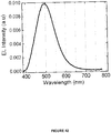
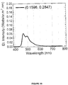
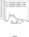
- Device lifetime is a particularly important issue for blue emitting phosphorescent devices, i.e., devices having a phosphorescent material with an emission spectra with its peak at a wavelength between 440 nm and 500 nm. This is because blue photons are the highest energy photons in the visible spectrum, such that blue emitting organic molecules generally have correspondingly higher triplet and / or singlet energies. As a result, many materials in a blue emitting device may be exposed to higher energy excitons and / or charge carriers than other devices.
- the selection of materials available for use in a blue device may be limited by constraints on particular properties relating to highest occupied molecular orbitals, lowest unoccupied molecular orbitals, band gap, etc., in order to ensure proper charge transport in the device, whereas the constraints on devices emitting lower energy photons may be more relaxed. Because the selection of materials for blue devices is limited, some of the more desirable materials used for devices that emit green or red may not be viable choices for blue emitting devices. Device lifetime is also important for green emitting devices, i.e., devices having a phosphorescent material with an emission spectra with its peak at a wavelength between 500 nm and 530 nm. Some of the same issues described for blue devices apply to green devices, but to a lesser extent. Thus, many of the features described herein are particularly desirable for use in devices having these wavelengths, particularly blue. However, the features may be used in devices that emit any color.
- the total thickness of first organic layer 330 and second organic layer 340 is at least 400 ⁇ , and the thickness of first organic layer 330 is at least 50 ⁇ and the thickness of second organic layer 340 is at least 50 ⁇ .
- the total thickness of first and second organic layers 330 and 340 is sufficiently large to allow for a wide recombination zone.
- the minimum thicknesses for each of the layers means that the interface between first and second organic layers 330 and 340, at which or near much of the recombination may occur, is at least 50 ⁇ away from other layers that may contain other materials. As a result, any device lifetime issues caused by such other materials may be reduced.
- the phosphorescent material has a highest occupied molecular orbital that is at least 0.3 eV higher than the highest occupied molecular orbital of the non-emissive material.
- hole transport in first and second organic layers 330 and 340 will occur predominantly on the phosphorescent material.
- the difference in concentration of the phosphorescent material between first and second layers 330 and 340 is likely to result in a significant difference in the hole transport properties of the two layers, such that recombination occurs at or near the interface between the two layers.
- hole blocking layer 350 When hole blocking layer 350 is present, there are several preferred material selections for the layer. Without intending to be limited to any theory as to why aspects of the invention work, the purpose of hole blocking layer 350 is to prevent holes from moving from second organic layer 340 into hole blocking layer 350. Hole blocking layer 350 is disposed between second organic layer 340 and cathode 360, and is in direct contact with second organic layer 340. Layer 350 may also be referred to as a "fourth" organic layer.
- One way to prevent holes from moving into hole blocking layer 350 is to use the non-emissive material of first and second organic layers 330 and 340 for hole blocking layer 350. Because the phosphorescent material of first and second organic layers 330 and 340 is not present in hole blocking layer 350, and that material is responsible for hole transport in first and second organic layers 330 and 340, holes may not be able to enter hole blocking layer 350. This is particularly true where the phosphorescent material has a highest occupied molecular orbital that is at least 0.3 eV higher than the highest occupied molecular orbital of the non-emissive material, as described above. The use of this particular non-emissive material in hole blocking layer 350 is desirable for several reasons.
- hole blocking layer 350 includes only the non-emissive material of first and second organic layers 330 and 340, possibly with minor impurities that do not affect device properties.
- other materials may also be used for hole blocking layer 350, such as materials having highest occupied molecular orbitals at least 0.3 eV higher then that of the phosphorescent material of second organic layer 340.
- Layer 350 may also serve to block excitons from leaving second organic layer 340.
- layer 350 includes only materials having a triplet energy at least 0.1 eV higher than the triplet energy of the emissive dopant.
- FIG. 4 shows an organic light emitting device with an emissive layer having first and second organic layers with different concentrations of phosphorescent material and non-emissive materials, and no organic layers between the first organic layer and the anode.
- the device of FIG. 4 includes a substrate 410, an anode 415, an emissive layer having a first organic layer 430 and a second organic layer 440, a hole blocking layer 450, an electron transport layer 460, and a cathode 470.
- Hole blocking layer 450 and electron transport layer 460 are optional.
- First organic layer 430 is disposed between the anode and the cathode, and includes a phosphorescent material and a non-emissive material.
- the concentration of the phosphorescent material in the first organic layer is 10 - 90 wt%.
- the concentration of the non-emissive material in the first organic layer is 10 - 90 wt%.
- Second organic layer 440 is disposed between the first organic layer and the cathode, and is in direct contact with first organic layer 430.
- Second organic layer includes the phosphorescent material and the non-emissive material of the first organic layer.
- the concentration of the phosphorescent material in the second layer is 3 - 25 wt%.
- the concentration of the non-emissive material in the second organic layer is 75-97 wt%.
- the concentration of the phosphorescent material in the second organic layer is lower than the concentration of the phosphorescent material in the first organic layer.
- first and second organic layers 430 and 440 include only the phospho
- the device of FIG. 4 relies on a combination of features to achieve a long-lived device. Simply avoiding the use of any organic layers between the anode and an emissive layer is not likely to result in a good device, because of issues caused by the anode-emissive layer interface, and particularly by recombination at or near that interface. However, the device of FIG. 4 also includes different layers with different concentrations of phosphorescent emissive dopant. As with the device of FIG.
- the device of FIG. 4 avoids issues that may have been present in prior devices with an emissive layer in contact with an anode.
- the device of FIG. 4 also avoids issues that may have been present in prior devices caused by electron damage to organic materials between the emissive layer and the anode, because the device of FIG. 4 does not have any such organic materials to be damaged by electrons.
- FIG. 5 shows an organic light emitting device having only three organic materials.
- the device of FIG. 5 includes a substrate 510, an anode 515, a third organic layer 520, an emissive layer having a first organic layer 530 and a second organic layer 540, a hole blocking layer 550, an electron transport layer 560, and a cathode 570.
- First organic layer 530 is disposed between the anode and the cathode, and includes a phosphorescent material and a non-emissive material.
- the concentration of the phosphorescent material in the first organic layer is 10 - 90 wt%.
- the concentration of the non-emissive material in the first organic layer is 10 - 90 wt%.
- Second organic layer 540 is disposed between the first organic layer and the cathode, and is in direct contact with first organic layer 530.
- Second organic layer includes the phosphorescent material and the non-emissive material of the first organic layer.
- the concentration of the phosphorescent material in the second layer is 3 - 25 wt%.
- the concentration of the non-emissive material in the second organic layer is 75-97 wt%.
- the concentration of the phosphorescent material in the second organic layer is lower than the concentration of the phosphorescent material in the first organic layer.
- First and second organic layers 530 and 540 include only the phospho
- Third organic layer 520 includes only the phosphorescent material of first organic layer 530, and is in direct contact with first organic layer 530.
- the phosphorescent material may not actually emit, but rather may serve to transport holes from anode 515 and inject the holes into first organic layer 530.
- Hole blocking layer 550 includes only the non-emissive material of first organic layer 530. Without being limited to any theory as to how aspects of the invention work, it is believed that hole transport in first and second layers 530 and 540 occurs on the phosphorescent material, and that such transport does not occur on the non-emissive material. As a result, hole blocking layer 550 is unable to transport holes from second organic layer 540, and acts as a hole blocking layer.
- third organic layer 520 there are only two organic materials used between third organic layer 520, first organic layer 530, second organic layer 540, and third organic layer 550.
- the third organic material in the device of FIG. 5 is an electron transporting material present as the only material in electron transport layer 560.
- the phosphorescent material is the emissive material of the device.
- the device of FIG. 5 may be modified in a limited way to include a fourth organic material, such that the device includes only four organic materials, and one of the organic materials is an electron transport material present in the device only between the emissive layer and the cathode.
- a fourth organic material such that the device includes only four organic materials, and one of the organic materials is an electron transport material present in the device only between the emissive layer and the cathode.
- the device may include two different phosphorescent materials and a single non-emissive material in the emissive layer, a single phosphorescent material and two different non-emissive materials in the emissive layer, or a phosphorescent material, a non-emissive material, and a lower energy emissive material.
- FIG. 6 shows an organic light emitting device similar to that of FIG. 3 , but including multiple phosphorescent materials.
- the device of FIG. 6 includes a substrate 610, an anode 615, a third organic layer 620, an emissive layer having a first organic layer 630 and a second organic layer 640, a hole blocking layer 650, an electron transport layer 660, and a cathode 670.
- Third organic layer 620, hole blocking layer 650 and electron transport layer 660 are optional.
- First organic layer 630 is disposed between the anode and the cathode, and includes a first phosphorescent material and a non-emissive material.
- the concentration of the first phosphorescent material in the first organic layer is 3-50 wt%.
- the concentration of the non-emissive material in the first organic layer is 10 - 97 wt%.
- Second organic layer 640 is disposed between first organic layer 630 and the cathode, and is in direct contact with first organic layer 630.
- Second organic layer 640 includes the first phosphorescent material and the non-emissive material of the first organic layer.
- the concentration of the first phosphorescent material in the second layer is 3 - 25 wt%.
- the concentration of the non-emissive material in the second organic layer is 10-90 wt%.
- the concentration of the first phosphorescent material in the second organic layer is lower than the concentration of the phosphorescent material in the first organic layer.
- First organic layer 630, second organic layer 640, or both, include a lower energy emissive material present in a concentration 0.1-12 wt%.
- the lower energy emissive material may be a fluorescent emissive material. Where the lower energy emissive material is fluorescent, the device may exhibit phosphorescent-sensitized fluorescent emission, i.e., energy may be transferred from triplets on the first phosphorescent material to the fluorescent emissive material.
- Both first organic layer 630 and second organic layer 640 may include the lower energy emissive material present in a concentration 0.1-12 wt%. Or, only first organic layer 630 may include the lower energy emissive material present in a concentration 0.1-12 wt%, while second organic layer 640 does not include the lower energy emissive material. Or, only second organic layer 640 may include the lower energy emissive material present in a concentration 0.1-12 wt%, while first organic layer 630 does not include the lower energy emissive material.
- first organic layer 630 includes only the first phosphorescent material and the non-emissive material
- second organic layer 640 includes only the first phosphorescent material, the non-emissive material, and the lower energy emissive material.
- the concentration of the non-emissive material in the first organic layer is 50 - 97 wt%
- the concentration of the non-emissive material in the second organic layer is 63 - 90 wt%.
- Both the first phosphorescent material and the lower energy emissive material may emit in the device of FIG. 6 .
- the first phosphorescent material is the only emissive material present in first organic layer 630, it may emit from that layer.
- the lower energy emissive material is phosphorescent with a lower triplet energy than the first phosphorescent material, emission from the second phosphorescent material may be favored in second organic layer 640.
- first phosphorescent material may emit from first organic layer 630.
- the device of FIG. 6 may have multiple emissive materials with different emission spectra, such that a broad overall emission for the device may be achieved. Such an emission spectrum is desirable for certain applications, such as general illumination.
- FIG. 7 shows an organic light emitting device with an emissive layer having first and second organic layers with different concentrations of phosphorescent material and non-emissive materials, and organic layers between the first organic layer and the cathode with specific charge carrier mobility characteristics.
- the device of FIG. 7 applies concepts similar to those described for FIG. 3 , but as applied to a device where a phosphorescent material is predominantly responsible for electron transport in the emissive layer and not hole transport. While the most common phosphorescent devices do not include an emissive layer where electrons are transported on the phosphorescent material, it is believed that Compound S is an example of a phosphorescent molecule that may transport electrons in an emissive layer.
- the device of FIG. 7 includes a substrate 710, an anode 715, a third organic layer 720, a first organic layer 730, a second organic layer 740, a hole blocking layer 750, an electron transport layer 760, and a cathode 770.
- Third organic layer 720, hole blocking layer 750 and electron transport layer 760 are optional.
- First organic layer 730 is disposed between the anode and the cathode, and includes a phosphorescent material and a non-emissive material.
- the concentration of the phosphorescent material in the first organic layer is 3 - 25 wt%.
- the concentration of the non-emissive material in the first organic layer is 75 - 97 wt%.
- Second organic layer 740 is disposed between the first organic layer and the cathode, and is in direct contact with first organic layer 730.
- Second organic layer 740 includes the phosphorescent material and the non-emissive material of the first organic layer.
- the concentration of the phosphorescent material in the second organic layer is 10 - 90 wt%.
- the concentration of the non-emissive material in the second organic layer is 10 - 90 wt%.
- the concentration of the phosphorescent material in the second organic layer is higher than the concentration of the phosphorescent material in the first organic layer.
- the device of FIG. 7 operates on a principle similar to that of FIG. 3 , but different in that is intended for material combinations where a phosphorescent emissive dopant is responsible for electron transport, but not hole transport.
- second organic layer 740 which closer to cathode 770 than first organic layer 730, has a higher concentration of the electron-transporting phosphorescent material than first organic layer 730.
- electron mobility should drop in first organic layer 730 relative to second organic layer 740, such that recombination may occur at or near the interface between first organic layer 730 and second organic layer 740.
- FIG. 8 shows an organic light emitting device that was fabricated using the parameters in Tables 1 and 3.
- FIG. 9 shows a specific organic light emitting device that was fabricated and tested, having first and second organic layers with different concentrations of phosphorescent material and non-emissive materials.
- FIG. 10 shows a specific organic light emitting device that was fabricated and tested.
- the device of FIG. 10 includes only four organic materials: COMPOUND A, COMPOUND F, mCBP and Alq.
- the device of FIG. 10 includes, in order, an ITO anode, a 10 nm thick hole injection layer of COMPOUND A, a 60 nm thick emissive layer of mCBP doped with 15% COMPOUND F, a 5 nm thick hole blocking layer of mCBP, a 20 nm thick electron transport layer of Alq, a 0.5 nm thick inorganic electron injection layer of LiF, and a 100 nm thick Al cathode.
- FIG. 11 shows a plot of current density versus voltage for the device of FIG. 10 .
- FIG. 12 shows a plot of external quantum efficiency (EQE) versus current density for the device of FIG. 10 .
- FIG. 13 shows a plot of normalized intensity (arbitrary units) versus time for the device of FIG. 10 .
- FIG. 14 shows a plot of normalized electroluminescent intensity versus wavelength for the device of FIG. 10 .
- FIG. 15 shows a specific organic light emitting device that was fabricated and tested.
- the device of FIG. 15 includes only three organic materials: COMPOUND F, mCBP and Alq.
- the device of FIG. 15 includes, in order, an ITO anode, a 10 nm thick hole injection layer of COMPOUND F, a 60 nm thick emissive layer of mCBP doped with 15% COMPOUND F, a 5 nm thick hole blocking layer of mCBP, a 20 nm thick electron transport layer of Alq, a 0.5 nm thick inorganic electron injection layer of LiF, and a 100 nm thick Al cathode.
- the device of FIG. 15 is similar to the device of FIG. 10 , except that COMPOUND F is used for the hole injection layer instead of COMPOUND A.
- COMPOUND F is also the emissive material in the device of FIG. 15 .
- FIG. 16 shows a plot of current density versus voltage for the device of FIG. 15 .
- FIG. 17 shows a plot of external quantum efficiency (EQE) versus current density for the device of FIG. 15 .
- FIG. 18 shows a plot of normalized intensity (arbitrary units) versus time for the device of FIG. 15 .
- FIG. 19 shows a plot of normalized electroluminescent intensity versus wavelength for the device of FIG. 15 .
- FIG. 20 shows plots of normalized luminescence versus time for various device structures.
- the device of FIG. 15 and the experimental results plotted in FIGS. 16-19 , show that the device of FIG. 15 has measured results similar to that of FIG. 10 . This is evidence that COMPOUND F is a good hole transporter, similar to COMPOUND A. If COMPOUND F did not have hole transport properties comparable to those of COMPOUND A, it would be expected that the device of FIG. 15 would exhibit poorer performance than that of FIG. 10 as a result of COMPOUND F being less able to transport holes.
- FIG. 21 shows an organic light emitting device that was fabricated using the parameters in Table 2, having first and second organic layers with different concentrations of phosphorescent material and non-emissive materials.
- FIG. 22 shows an organic light emitting device that was fabricated using the parameters in Table 4, having first and second organic layers with different concentrations of phosphorescent material and non-emissive materials.
- Table 5 shows device performance for the devices of Table 4.
- Table 4 HIL1 HIL2 HTL EML BL 100 ⁇
- Example 6 Compound A none Compound D: Compound E 30% 300 ⁇ Compound D: Compound E 10% 300 ⁇ Compound D
- Example 7 Compound A none Compound C: Compound A 30% 300 ⁇ Compound C: Compound A 10% ⁇ Compound C
- FIG. 23 shows plots of normalized electroluminescent intensity versus wavelength for devices fabricated according to FIG. 22 using parameters from Table 4.
- FIG. 24 shows plots of luminous efficiency versus luminance for devices fabricated according to FIG. 22 using parameters from Table 4.
- FIG. 25 shows plots of external quantum efficiency versus luminance for devices fabricated according to FIG. 22 using parameters from Table 4.
- FIG. 26 shows plots of current density versus voltage for devices fabricated according to FIG. 22 using parameters from Table 4.
- FIG. 27 shows plots of luminance versus voltage for devices fabricated according to FIG. 22 using parameters from Table 4.
- FIG. 28 shows plots of normalized luminance versus time for devices fabricated according to FIG. 22 using parameters from Table 4.
- FIG. 29 shows an organic light emitting device that was fabricated using the parameters in Table 6, having first and second organic layers with different concentrations of phosphorescent material and non-emissive materials, some devices with a layer of NPD and some without a layer of NPD.
- the data in Table 6 shows that the introduction of a 100 ⁇ layer of NPD between a hole injection layer and an emissive layer reduces the lifetime of a red emitting device.
- Table 6 HIL layers (100 ⁇ each) CIE At 1,000 nits At 40mA/cm 2 X Y Voltage [v] L.E. [cd/A] EQE [%] P.E.
- FIG. 30 shows an organic light emitting device without a layer of NPD.
- FIG. 31 shows an organic light emitting device with a layer of NPD.
- FIG. 32 shows plots of external quantum efficiency versus luminance for the devices of FIG. 30 and FIG. 31 .
- FIG. 33 shows plots of power efficacy versus luminance for the devices of FIG. 30 and FIG. 31 .
- FIG. 34 shows plots of luminance versus voltage for the devices of FIG. 30 and FIG. 31 .
- FIG. 35 shows plots of electroluminescent intensity versus wavelength for the devices of FIG. 30 and FIG. 31 .
- FIG. 36 shows plots of normalized luminance versus time for the device of FIG. 30 at various initial luminances.
- FIG. 37 shows plots of normalized luminance versus time for the device of FIG. 31 at various initial luminances.
- FIG. 38 shows an organic light emitting device that has emission from both NPD and BAlq.
- FIG. 39 shows a plot of external quantum efficiency versus luminance for the device of FIG. 38 .
- FIG. 40 shows a plot of power efficacy versus luminance for the device of FIG. 38 .
- FIG. 41 shows a plot of luminance versus voltage for the device of FIG. 38 .
- FIG. 42 shows a plot of electroluminescent intensity (arbitrary units) versus wavelength for the device of FIG. 38 .
- FIG. 43 shows a plot of normalized luminance versus time for the device of FIG. 38 .
- FIG. 44 shows an organic light emitting device that has emission only from Alq.
- FIG. 45 shows a plot of external quantum efficiency versus luminance for the device of FIG. 44 .
- FIG. 46 shows a plot of power efficacy versus luminance for the device of FIG. 44 .
- FIG. 47 shows a plot of luminance versus voltage for the device of FIG. 44 .
- FIG. 48 shows a plot of electroluminescent intensity (arbitrary units) versus wavelength for the device of FIG. 44 .
- FIG. 49 shows a plot of normalized luminance versus time for the device of FIG. 44 .
- FIG. 50 shows an organic light emitting device having only a layer with a high hole conductivity between an emissive layer and the anode, and a hole blocking layer of the same material used as a non-emissive host in the emissive layer.
- the device of FIG. 50 includes a 10 nm thick hole injection layer of LG101, a 60 nm thick first organic emissive layer of COMPOUND J doped with 15 wt% COMPOUND H, a 25 nm thick hole blocking layer of COMPOUND J, a 20 nm thick electron transport layer of Alq, and a LiF / Al cathode.
- FIG. 51 shows a plot of normalized luminescence versus time for the device of FIG. 50 .
- FIG. 52 shows a plot of external quantum efficiency versus luminance for the device of FIG. 50 .
- FIG. 53 shows a plot of power efficacy versus luminance for the device of FIG. 50 .
- FIG. 54 shows a plot of luminance versus voltage for the device of FIG. 50 .
- FIG. 55 shows a plot of EL intensity versus wavelength for the device of FIG. 50 .
- FIG. 56 shows an organic light emitting device having only a layer with a high hole conductivity between an emissive layer and the anode, a hole blocking layer of the same material used as a non-emissive host in the emissive layer, and an emissive layer having first and second organic layers with different concentrations of phosphorescent material and non-emissive materials, where the concentration of phosphorescent material in the second organic layer is variable.
- FIG. 57 The device of FIG. 56 is very similar to that of FIG. 50 , with the difference being that there is a step in the concentration of dopant H in the device of FIG. 56 , but not in the device of FIG. 50 .
- FIG. 57 shows a plot of normalized luminescence versus time for the device of FIG. 56 .
- FIG. 58 shows a plot of external quantum efficiency versus luminance for the device of FIG. 56 .
- FIG. 59 shows a plot of power efficacy versus luminance for the device of FIG. 56 .
- FIG. 60 shows a plot of luminance versus voltage for the device of FIG. 56 .
- FIG. 61 shows a plot of EL intensity versus wavelength for the device of FIG. 56 .
- the device of FIG. 56 may be compared to the device of FIG. 50 .
- the devices are similar except in the emissive layer, where the device of FIG. 56 has a step in the concentration of COMPOUND H, whereas the device of FIG. 50 does not.
- the measured results for these two devices show that the device of FIG. 56 has a lower operating voltage, enabled by the step in dopant concentration.
- the device of FIG. 56 also has better blue CIE coordinates that the device of FIG. 50 . It is believed that the better CIE coordinates are due to optical effects resulting from recombination closer to the cathode in the device of FIG. 56 , due to increased hole conductivity in the layer doped with 30% COMPOUND H.
- the device of FIG. 56 also exhibits higher external quantum efficiency than the device of FIG. 50 . It is believed that the higher efficiency in the device of FIG. 56 is due to more spread out recombination due to the step in dopant concentration, and a better balance of electrons and holes at the recombination location. In addition, recombination often occurs at interfaces, and the device of FIG. 56 has three interfaces involving a layer that can emit light due to the step in concentration, whereas the device of FIG. 50 has only two such interfaces.
- FIG. 62 shows an organic light emitting device having only a layer with a high hole conductivity between an emissive layer and the anode, a hole blocking layer of the same material used as a non-emissive host in the emissive layer, and an emissive layer having first and second organic layers with different phosphorescent materials in the first and second organic emissive layers, where the concentration of phosphorescent material in the second organic emissive layer is variable.
- 62 includes a 10 nm thick hole injection layer of LG101, a 30 nm thick first organic emissive layer of COMPOUND J doped with 30 wt% COMPOUND A, a 30 nm thick second organic emissive layer of COMPOUND J doped with X wt% COMPOUND H, a 25 nm thick hole blocking layer of COMPOUND J, a 20 nm thick electron transport layer of Alq, and a LiF / Al cathode.
- the device of FIG. 62 is very similar to that of FIG.
- the device of FIG. 62 uses different emissive phosphorescent material in the first and second organic emissive layers, while the device of FIG. 56 uses the same phosphorescent material in both layers.
- the concentrations of the phosphorescent materials are the same in the device of FIG. 56 compared to the device of FIG. 62 .
- FIG. 63 shows a plot of external quantum efficiency versus luminance for the device of FIG. 62 .
- FIG. 64 shows a plot of power efficacy versus luminance for the device of FIG. 62 .
- FIG. 65 shows a plot of luminance versus voltage for the device of FIG. 62 .
- FIG. 66 shows a plot of EL intensity versus wavelength for the device of FIG. 62 .
- the device of FIG. 62 may be compared to the device of FIG. 56 .
- the devices are similar except in the emissive layer, where the device of FIG. 62 has an emissive layer doped with phosphorescent emitter COMPOUND A and another emissive layer doped phosphorescent emitter COMPOUND H, whereas the device of FIG. 56 has only phosphorescent emitter COMPOUND H.
- Both devices have a step in dopant concentration, and similar concentrations even in the layers where the actual dopant is different.
- the device of FIG. 62 exhibits a broad emission spectra that is a combination of emission from both COMPOUND A and COMPOUND H.
- the device of FIG. 56 is emitting from both the layer doped with 30% COMPOUND H and the layer doped with a lesser concentration of COMPOUND H. Comparing FIG. 58 to FIG. 63 , it can be seen that the device of FIG. 62 has better charge balance than the device of FIG. 56 , as evidenced by a relatively flat external quantum efficiency over three orders of magnitude for the device of FIG. 62 as compared to two orders of magnitude for the device of FIG. 56 .
- a number of devices were fabricated having two different doped emissive layers, where the devices do not include a hole transport layer using a material such as NPD. Table 7 shows the structures for these devices. Table 8 shows measured experimental results for these devices.
- the devices had an ITO anode, a hole injection layer of LG101, and an emissive layer having a first organic layer and a second organic layer with an interface in between. Some of the devices had a hole blocking layer. All of the devices had an electron transport layer of LG201, available from the same source as LG101, and an LiF / Al cathode.
- Devices 1, 2 and 4 include the same non-emissive material in the first and second organic layers, but different phosphorescent materials.
- Devices 5 - 8 have first and second organic layers with different non-emissive materials and different phosphorescent materials.
- Devices 9, 11 and 12 have first and second organic layers with different non-emissive materials and different phosphorescent materials, where the first organic layer additionally includes an emissive material.
- Devices 13 -22 have first and second organic layers with the same non-emissive materials, and different phosphorescent materials, where the first organic layer additionally includes a lower energy emissive material. All of devices 1, 2, 4, 5-8, 9, 11, 12, and 13-22 include emissive layers having a first and second organic layer with an interface in between. In most of these devices, the concentration of phosphorescent material is higher in the first (closer to anode) organic layer.
- the emissive layer of Device 3 does not include first and second organic layers, each having a non-emissive material and a phosphorescent material, with an interface in between. Neither does the emissive layer of Device 10, because Compound B is non-emissive in Device 10. and 10 do not include first and second organic layers, each having a non-emissive material and a phosphorescent material.
- Table 9 shows device structures and measured experimental results for some devices having an emissive layer with an interface between a first organic layer and a second organic layer, where the host and the dopant, i.e., the non-emissive material is the same material in both layers and the phosphorescent material is the same material in both layers, but the concentrations are different. All of the devices in Table 9 had a 100 ⁇ hole injection layer of Compound A, a 100 ⁇ hole blocking layer ("BL”) of different materials depending on the specific device, a 400 ⁇ electron transport layer, and an LiF / Al cathode.
- BL 100 ⁇ hole blocking layer
- the emissive layer included a first organic layer and a second organic layer with an interface between them, where the first organic layer was 300 ⁇ of a non-emissive material (the "host” in Table 9) at a concentration of 70 wt% and a phosphorescent material (the “dopant” of Table 9) at a concentration of 30 wt%, and the second organic layer was 300 ⁇ of the same non-emissive material (the "host” in Table 9) but at a concentration of 90 wt% and the same phosphorescent material (the “dopant” of Table 9) but at a concentration of 10 wt%.
- the specific host and dopant for each device are identified in Table 9.
- the general device structure for the devices of Table 9 was: ITO (1200 ⁇ ) / Compound A (100 ⁇ ) / host (70 wt%):dopant (30 wt%) (300 ⁇ ) / host (90 wt%):dopant (10 wt%) (300 ⁇ ) / BL (100 ⁇ ) / Alq 3 (400 ⁇ ) / LiF / Al.
- Table 9 Example CIE At 1,000 nits At 40mA/cm 2 Host Dopant BL X Y Voltage [v] L.E. [cd/A] E.Q.E. [%] P.E.
Description
- The present invention relates to organic light emitting devices (OLEDs). More specifically, the present invention relates to OLEDs having particular structures that may enhance lifetime.
- Opto-electronic devices that make use of organic materials are becoming increasingly desirable for a number of reasons. Many of the materials used to make such devices are relatively inexpensive, so organic opto-electronic devices have the potential for cost advantages over inorganic devices. In addition, the inherent properties of organic materials, such as their flexibility, may make them well suited for particular applications such as fabrication on a flexible substrate. Examples of organic opto-electronic devices include organic light emitting devices (OLEDs), organic phototransistors, organic photovoltaic cells, and organic photodetectors. For OLEDs, the organic materials may have performance advantages over conventional materials. For example, the wavelength at which an organic emissive layer emits light may generally be readily tuned with appropriate dopants.
- OLEDs make use of thin organic films that emit light when voltage is applied across the device. OLEDs are becoming an increasingly interesting technology for use in applications such as flat panel displays, illumination, and backlighting. Several OLED materials and configurations are described in
U.S. Pat. Nos. 5,844,363 ,6,303,238 , and5,707,745 . - One application for phosphorescent emissive molecules is a full color display. Industry standards for such a display call for pixels adapted to emit particular colors, referred to as "saturated" colors. In particular, these standards call for saturated red, green, and blue pixels. Color may be measured using CIE coordinates, which are well known to the art.
- One example of a green emissive molecule is tris(2-phenylpyridine) iridium, denoted Ir(ppy)3, which has the structure of Formula I:

- In this, and later figures herein, we depict the dative bond from nitrogen to metal (here, Ir) as a straight line.
- As used herein, the term "organic" includes polymeric materials as well as small molecule organic materials that may be used to fabricate organic opto-electronic devices. "Small molecule" refers to any organic material that is not a polymer, and "small molecules" may actually be quite large. Small molecules may include repeat units in some circumstances. For example, using a long chain alkyl group as a substituent does not remove a molecule from the "small molecule" class. Small molecules may also be incorporated into polymers, for example as a pendent group on a polymer backbone or as a part of the backbone. Small molecules may also serve as the core moiety of a dendrimer, which consists of a series of chemical shells built on the core moiety. The core moiety of a dendrimer may be a fluorescent or phosphorescent small molecule emitter. A dendrimer may be a "small molecule," and it is believed that all dendrimers currently used in the field of OLEDs are small molecules.
- As used herein, "top" means furthest away from the substrate, while "bottom" means closest to the substrate. Where a first layer is described as "disposed over" a second layer, the first layer is disposed further away from substrate. There may be other layers between the first and second layer, unless it is specified that the first layer is "in contact with" the second layer. For example, a cathode may be described as "disposed over" an anode, even though there are various organic layers in between.
- As used herein, "solution processible" means capable of being dissolved, dispersed, or transported in and/or deposited from a liquid medium, either in solution or suspension form.
- A ligand is referred to as "photoactive" when it is believed that the ligand contributes to the photoactive properties of an emissive material.
- A first energy level (HOMO or LUMO) is considered "less than" or "lower" than a second energy level if it is lower on a conventional energy level diagram, which means that the first energy level would have a value that is more negative than the second energy level. A first energy level (HOMO or LUMO) is considered "higher" than a second energy level if it is higher on a conventional energy level diagram, which means that the first energy level would have a value that is less negative than the second energy level. For example, the HOMO of CBP -5.32 eV and the HOMO of TPBI is -5.70 eV, therefore the HOMO of CBP is 0.38 eV "higher" than the HOMO of TPBI. Similarly, the LUMO of mCP is -0.77 eV and the LUMO of CBP is -1.23 eV, therefore the LUMO of mCP is 0.46 eV "higher" than the LUMO of CBP. The above values were determined using density functional calculations performed using the Spartan 02 software package, available from Wavefunction Inc. of Irvine, Calif., at the B3LYP/6-31G* level. A pseudo potential option can be used for species containing heavy metals such as Ir(ppy)3. Density functional calculations have been demonstrated in the literature to be able to qualitatively predict energies of organic and inorganic compounds.
- More details on OLEDs, and the definitions described above, can be found in
US Pat. No. 7,279,704 . - As used herein, the term "consisting essentially of' one or more materials as applied to a layer in an organic light emitting device means that there may be materials present in addition to those listed, but any such additional materials are present only in minor quantities (such as impurities) and do not significantly affect the electronic properties or emissive of the device, i.e., they do not significantly contribute to the transport or trapping of holes or electrons, they do not result in a shift of the recombination location, and they do not significantly contribute to or participate in exciton decay, emissive or otherwise.
- Unless otherwise indicated, percentages of organic compounds in various layers described herein are weight percentages.
- The following two references including Samuel as a co-author describe solution processable phosphorescent OLEDs with doped emissive layer in direct contact with ITO. E.E.Namdas, T.D.Anthopoulos, I.D.W.Samuel, Applied physics letters 86, 161104 (2005). T.D.Anthopoulos, M.J.Frampton, E.B.Namdas, P.L.Burn, I.D.W.Samuel, Adv. Mater.2004, 16, No. 6, March 18, pp. 557-560.
-
EP1670082 ,US2005/0046337 ,JP2005038672 JP2003229272 US2006/0232194 ,US2005/0074630 disclose organic light emitting devices comprising phosphorescent light emitting layers with different phosphorescent material concentrations. - According to the invention, an organic light emitting device with an interface in the emissive layer is provided, as described in
claim 1. In a first aspect, the device has an anode, a cathode, and an emissive layer disposed between the anode and the cathode. The emissive layer includes a first organic layer, which includes a first phosphorescent material and a first non-emissive material. The concentration of the first phosphorescent material in the first organic layer is 10 - 90 wt%, and the concentration of the first non-emissive material in the first organic layer is 10 - 90 wt%. The emissive layer also includes a second organic layer which includes a second phosphorescent material and a second non-emissive material. The concentration of the second phosphorescent material in the second layer is 3 - 25 wt%, and the concentration of the second non-emissive material in the second organic layer is 75-97 wt%. The concentration of the second phosphorescent material in the second organic layer is lower than the concentration of the first phosphorescent material in the first organic layer, preferably at least 5 wt% lower, and more preferably at least 10 wt% lower. The first non-emissive material and the second non-emissive material may be the same material or different materials, and the first phosphorescent material and the second phosphorescent material may be the same material or different materials. Thus, there are four combinations: (1) same phosphorescent material in both first and second organic layers, and same non-emissive material in both first and second organic layers; (2) different phosphorescent material in the first and second organic layers, and same non-emissive material in both first and second organic layers; (3) same phosphorescent material in both first and second organic layers, and different non-emissive material in first and second organic layers; and (4) different phosphorescent material in the first and second organic layers, and different non-emissive material in the first and second organic layers. There are advantages to each combination. The first organic layer may consist essentially of the first phosphorescent material and the first non-emissive material, and the second organic layer may consist essentially of the first phosphorescent material and the first non-emissive material of the first organic layer. Device architectures that mitigate damage in the device and extend device lifetime are also provided for use with the first aspect, either individually or in combination. - The first organic layer, the second organic layer, or both, may optionally further include a lower energy emissive material, wherein the concentration of the lower energy emissive material is 0.1-12 wt%.
- In a second aspect, according to the invention, one architecture to mitigate damage is provided. All organic layers between the first organic layer and the anode have a hole mobility and an electron mobility such that the hole mobility is at least twice as great as the electron mobility, preferably at least ten times greater, and more preferably at least 100 times greater.
- In a third aspect, according to the invention, another architecture to mitigate damage is provided. All organic layers between the first organic layer and the anode do not include any materials containing a group selected from the group consisting of triarylamine, napthyl, tri(N-carbazoyl)triphenylamine, tetraarylamine and carbazole.
- In a fourth aspect, not according to the invention, another architecture to mitigate damage is provided. There are no organic layers between the first organic layer and the anode.
- In a fifth aspect, another architecture to mitigate damage is provided. A third organic layer is provided, disposed between the first organic layer and the anode. The third organic layer consists essentially of the first phosphorescent material. The third organic layer is in direct contact with the first organic layer and the anode, such that it is the only layer between the first organic layer and the anode.
- In a sixth aspect, another architecture to mitigate damage is provided. The device includes no more than three different organic materials, minimizing the number of materials subject to damage.
- In a seventh aspect, another architecture to mitigate damage is provided. The device includes no more than four different organic materials, where one of the organic materials is an electron transport material present in the device only between the emissive layer and the cathode. The limitation on the number of materials minimizes the number of materials subject to damage.
- In an eighth aspect, another architecture to mitigate damage is provided. All organic layers between the first organic layer and the anode consist essentially of organometallic materials.
- In a ninth aspect, another architecture to mitigate damage is provided. All organic layers between the first organic layer and the anode have a hole conductivity sufficiently large such that an additional 10 nm thickness in the layer results in a voltage rise of 0.1 V or less at a current of 10 mA / cm2.
- In a tenth aspect, another architecture to mitigate damage is provided. The first non-emissive material has a triplet energy of 2.7 eV or greater.
- In an eleventh aspect, a lower energy emissive material is provided that may be used with the first aspect, with or without the various damage mitigation architectures. The lower energy emissive material may be a fluorescent emissive material, a phosphorescent material, or a combination of the two where there are multiple lower energy emissive materials. The concentration of the lower energy emissive material may be 0.1-12 wt%, and a lower energy emissive material may be present in only the first organic layer, only the second organic layer, or in both layers. An organic layer including a lower energy emissive material may consist essentially of a phosphorescent material, a non-emissive material, and a lower energy emissive material.
- In a twelfth aspect, a device similar to that of the first aspect is provided, but the concentration of the phosphorescent material in the second organic layer is higher than the concentration of the phosphorescent material in the first organic layer, as opposed to lower. The concentration of the first phosphorescent material in the first organic layer is 3 - 25 wt%, and the concentration of the first non-emissive material in the first organic layer is 75 - 97 wt%. The concentration of the phosphorescent material in the second layer is 10 - 90 wt%, and the concentration of the non-emissive material in the second organic layer is 10 - 90 wt%. Various other aspects as described above may be used in conjunction with the twelfth aspect.
- In various aspects, the first organic layer may consist essentially of the first phosphorescent material and the first non-emissive material, and the second organic layer may consist essentially of the first phosphorescent material and the first non-emissive material of the first organic layer.
- In various aspects, the total thickness of the first and second organic layers is preferably at least 400 Å. The thickness of the first organic layer is preferably at least 50 Å and the thickness of the second organic layer is preferably at least 50 Å.
- In various aspects, the first phosphorescent material preferably has a highest occupied molecular orbital that is at least 0.3 eV higher than the highest occupied molecular orbital of the first non-emissive material, and the second phosphorescent material preferably has a highest occupied molecular orbital that is at least 0.3 eV higher than the highest occupied molecular orbital of the first non-emissive material.
- In various aspects, a fourth organic layer may be provided disposed between the second organic layer and the cathode. The fourth organic layer consists essentially of the second non-emissive material, and is in direct contact with the second organic layer.
- In various aspects, a fourth organic layer may be provided disposed between the second organic layer and the cathode. The fourth organic layer consists essentially of materials having a triplet energy at least 0.1 eV greater than the triplet energy of the second phosphorescent material, and the fourth organic layer is in direct contact with the second organic layer.
- In various aspects, the first non-emissive material may be selected from materials containing a group selected from the group consisting of triphenylene, carbazole, dibenzothiophene and dibenzothiophene coupled with carbazole.
- In various aspects, the first organic layer may be in direct contact with the second organic layer.
-
-
FIG. 1 shows an organic light emitting device. -
FIG. 2 shows an inverted organic light emitting device that does not have a separate electron transport layer. -
FIG. 3 shows an organic light emitting device having first and second organic layers with different concentrations of phosphorescent material and non-emissive materials, and organic layers between the first organic layer and the anode with specific charge carrier mobility characteristics. -
FIG. 4 shows an organic light emitting device, not according to the invention, having first and second organic layers with different concentrations of phosphorescent material and non-emissive materials, and no organic layers between the first organic layer and the anode. -
FIG. 5 shows an organic light emitting device having only three organic materials. -
FIG. 6 shows an organic light emitting device similar to that ofFIG. 3 , but including multiple phosphorescent materials. -
FIG. 7 shows an organic light emitting device having first and second organic layers with different concentrations of phosphorescent material and non-emissive materials, and organic layers between the first organic layer and the cathode with specific charge carrier mobility characteristics. -
FIG. 8 shows a general phosphorescent OLED structure. -
FIG. 9 shows a specific organic light emitting device that was fabricated and tested, having first and second organic layers with different concentrations of phosphorescent material and non-emissive materials. -
FIG. 10 shows a specific organic light emitting device that was fabricated and tested. -
FIG. 11 shows a plot of current density versus voltage for the device ofFIG. 10 . -
FIG. 12 shows a plot of external quantum efficiency (EQE) versus current density for the device ofFIG. 10 . -
FIG. 13 shows a plot of normalized intensity (arbitrary units) versus time for the device ofFIG. 10 . -
FIG. 14 shows a plot of normalized electroluminescent intensity versus wavelength for the device ofFIG. 10 . -
FIG. 15 shows a specific organic light emitting device that was fabricated and tested. -
FIG. 16 shows a plot of current density versus voltage for the device ofFIG. 15 . -
FIG. 17 shows a plot of external quantum efficiency (EQE) versus current density for the device ofFIG. 15 . -
FIG. 18 shows a plot of normalized intensity (arbitrary units) versus time for the device ofFIG. 15 . -
FIG. 19 shows a plot of normalized electroluminescent intensity versus wavelength for the device ofFIG. 15 . -
FIG. 20 shows plots of normalized luminescence versus time for various device structures. -
FIG. 21 shows an organic light emitting device that was fabricated using the parameters in Table 2, having first and second organic layers with different concentrations of phosphorescent material and non-emissive materials. -
FIG. 22 shows an organic light emitting device that was fabricated using the parameters in Table 4, having first and second organic layers with different concentrations of phosphorescent material and non-emissive materials. -
FIG. 23 shows plots of normalized electroluminescent intensity versus wavelength for devices fabricated according toFIG. 22 using parameters from Table 4. -
FIG. 24 shows plots of luminous efficiency versus luminance for devices fabricated according toFIG. 22 using parameters from Table 4. -
FIG. 25 shows plots of external quantum efficiency versus luminance for devices fabricated according toFIG. 22 using parameters from Table 4. -
FIG. 26 shows plots of current density versus voltage for devices fabricated according toFIG. 22 using parameters from Table 4. -
FIG. 27 shows plots of luminance versus voltage for devices fabricated according toFIG. 22 using parameters from Table 4. -
FIG. 28 shows plots of normalized luminance versus time for devices fabricated according toFIG. 22 using parameters from Table 4. -
FIG. 29 shows an organic light emitting device that was fabricated using the parameters in Table 6, having first and second organic layers with different concentrations of phosphorescent material and non-emissive materials, some devices with a layer of NPD and some without a layer of NPD. -
FIG. 30 shows an organic light emitting device without a layer of NPD. -
FIG. 31 shows an organic light emitting device with a layer of NPD. -
FIG. 32 shows plots of external quantum efficiency versus luminance for the devices ofFIG. 30 andFIG. 31 . -
FIG. 33 shows plots of power efficacy versus luminance for the devices ofFIG. 30 andFIG. 31 . -
FIG. 34 shows plots of luminance versus voltage for the devices ofFIG. 30 andFIG. 31 . -
FIG. 35 shows plots of electroluminescent intensity versus wavelength for the devices ofFIG. 30 andFIG. 31 . -
FIG. 36 shows plots of normalized luminance versus time for the device ofFIG. 30 at various initial luminances. -
FIG. 37 shows plots of normalized luminance versus time for the device ofFIG. 31 at various initial luminances. -
FIG. 38 shows an organic light emitting device that has emission from both NPD and BAlq. -
FIG. 39 shows a plot of external quantum efficiency versus luminance for the device ofFIG. 38 . -
FIG. 40 shows a plot of power efficacy versus luminance for the device ofFIG. 38 . -
FIG. 41 shows a plot of luminance versus voltage for the device ofFIG. 38 . -
FIG. 42 shows a plot of electroluminescent intensity (arbitrary units) versus wavelength for the device ofFIG. 38 . -
FIG. 43 shows a plot of normalized luminance versus time for the device ofFIG. 38 . -
FIG. 44 shows an organic light emitting device that has emission only from Alq. -
FIG. 45 shows a plot of external quantum efficiency versus luminance for the device ofFIG. 44 . -
FIG. 46 shows a plot of power efficacy versus luminance for the device ofFIG. 44 . -
FIG. 47 shows a plot of luminance versus voltage for the device ofFIG. 44 . -
FIG. 48 shows a plot of electroluminescent intensity (arbitrary units) versus wavelength for the device ofFIG. 44 . -
FIG. 49 shows a plot of normalized luminance versus time for the device ofFIG. 44 . -
FIG. 50 shows an organic light emitting device having only a layer with a high hole conductivity between an emissive layer and the anode, and a hole blocking layer of the same material used as a non-emissive host in the emissive layer. -
FIG. 51 shows a plot of normalized luminescence versus time for the device ofFIG. 50 . -
FIG. 52 shows a plot of external quantum efficiency versus luminance for the device ofFIG. 50 . -
FIG. 53 shows a plot of power efficacy versus luminance for the device ofFIG. 50 . -
FIG. 54 shows a plot of luminance versus voltage for the device ofFIG. 50 . -
FIG. 55 shows a plot of EL intensity versus wavelength for the device ofFIG. 50 . -
FIG. 56 shows an organic light emitting device having only a layer with a high hole conductivity between an emissive layer and the anode, a hole blocking layer of the same material used as a non-emissive host in the emissive layer, and an emissive layer having first and second organic layers with different concentrations of phosphorescent material and non-emissive materials, where the concentration of phosphorescent material in the second organic layer is variable. -
FIG. 57 shows a plot of normalized luminescence versus time for the device ofFIG. 56 . -
FIG. 58 shows a plot of external quantum efficiency versus luminance for the device ofFIG. 56 . -
FIG. 59 shows a plot of power efficacy versus luminance for the device ofFIG. 56 . -
FIG. 60 shows a plot of luminance versus voltage for the device ofFIG. 56 . -
FIG. 61 shows a plot of EL intensity versus wavelength for the device ofFIG. 56 . -
FIG. 62 shows an organic light emitting device having only a layer with a high hole conductivity between an emissive layer and the anode, a hole blocking layer of the same material used as a non-emissive host in the emissive layer, and an emissive layer having first and second organic layers with different phosphorescent materials in the first and second organic emissive layers, where the concentration of phosphorescent material in the second organic emissive layer is variable. -
FIG. 63 shows a plot of external quantum efficiency versus luminance for the device ofFIG. 62 . -
FIG. 64 shows a plot of power efficacy versus luminance for the device ofFIG. 62 . -
FIG. 65 shows a plot of luminance versus voltage for the device ofFIG. 62 . -
FIG. 66 shows a plot of EL intensity versus wavelength for the device ofFIG. 62 . - Generally, an OLED comprises at least one organic layer disposed between and electrically connected to an anode and a cathode. When a current is applied, the anode injects holes and the cathode injects electrons into the organic layer(s). The injected holes and electrons each migrate toward the oppositely charged electrode. When an electron and hole localize on the same molecule, an "exciton," which is a localized electron-hole pair having an excited energy state, is formed. Light is emitted when the exciton relaxes via a photoemissive mechanism. In some cases, the exciton may be localized on an excimer or an exciplex. Non-radiative mechanisms, such as thermal relaxation, may also occur, but are generally considered undesirable.
- The initial OLEDs used emissive molecules that emitted light from their singlet states ("fluorescence") as disclosed, for example, in
U.S. Pat. No. 4,769,292 . Fluorescent emission generally occurs in a time frame of less than 10 nanoseconds. - More recently, OLEDs having emissive materials that emit light from triplet states ("phosphorescence") have been demonstrated. Baldo et al., "Highly Efficient Phosphorescent Emission from Organic Electroluminescent Devices," Nature, vol. 395, 151-154, 1998; ("Baldo-I") and Baldo et al., "Very high-efficiency green organic light-emitting devices based on electrophosphorescence," Appl. Phys. Lett., vol. 75, No. 3, 4-6 (1999) ("Baldo-II"). Phosphorescence is described in more detail in
US Pat. No. 7,279,704 at cols. 5-6. -
FIG. 1 shows an organiclight emitting device 100. The figures are not necessarily drawn to scale.Device 100 may include asubstrate 110, ananode 115, ahole injection layer 120, ahole transport layer 125, anelectron blocking layer 130, anemissive layer 135, ahole blocking layer 140, anelectron transport layer 145, anelectron injection layer 150, aprotective layer 155, and acathode 160.Cathode 160 is a compound cathode having a firstconductive layer 162 and a secondconductive layer 164.Device 100 may be fabricated by depositing the layers described, in order. The properties and functions of these various layers, as well as example materials, are described in more detail inUS 7,279,704 at cols. 6-10. - More examples for each of these layers are available. For example, a flexible and transparent substrate-anode combination is disclosed in
U.S. Pat. No. 5,844,363 . An example of a p-doped hole transport layer is m-MTDATA doped with F.sub.4-TCNQ at a molar ratio of 50:1, as disclosed inU.S. Patent Application Publication No. 2003/0230980 . Examples of emissive and host materials are disclosed inU.S. Pat. No. 6,303,238 to Thompson et al. An example of an n-doped electron transport layer is BPhen doped with Li at a molar ratio of 1:1, as disclosed inU.S. Patent Application Publication No. 2003/0230980 ,U.S. Pat. Nos. 5,703,436 and5,707,745 , disclose examples of cathodes including compound cathodes having a thin layer of metal such as Mg:Ag with an overlying transparent, electrically-conductive, sputter-deposited ITO layer. The theory and use of blocking layers is described in more detail inU.S. Pat. No. 6,097,147 andU.S. Patent Application Publication No. 2003/0230980 . Examples of injection layers are provided inU.S. Patent Application Publication No. 2004/0174116 . A description of protective layers may be found inU.S. Patent Application Publication No. 2004/0174116 . -
FIG. 2 shows aninverted OLED 200. The device includes asubstrate 210, acathode 215, anemissive layer 220, ahole transport layer 225, and ananode 230.Device 200 may be fabricated by depositing the layers described, in order. Because the most common OLED configuration has a cathode disposed over the anode, anddevice 200 hascathode 215 disposed underanode 230,device 200 may be referred to as an "inverted" OLED. Materials similar to those described with respect todevice 100 may be used in the corresponding layers ofdevice 200.FIG. 2 provides one example of how some layers may be omitted from the structure ofdevice 100. - The simple layered structure illustrated in
FIGS. 1 and2 is provided by way of nonlimiting example, and it is understood that embodiments of the invention may be used in connection with a wide variety of other structures. The specific materials and structures described are exemplary in nature, and other materials and structures may be used. Functional OLEDs may be achieved by combining the various layers described in different ways, or layers may be omitted entirely, based on design, performance, and cost factors. Other layers not specifically described may also be included. Materials other than those specifically described may be used. Although many of the examples provided herein describe various layers as comprising a single material, it is understood that combinations of materials, such as a mixture of host and dopant, or more generally a mixture, may be used. Also, the layers may have various sublayers. The names given to the various layers herein are not intended to be strictly limiting. For example, indevice 200,hole transport layer 225 transports holes and injects holes intoemissive layer 220, and may be described as a hole transport layer or a hole injection layer. In one embodiment, an OLED may be described as having an "organic layer" disposed between a cathode and an anode. This organic layer may comprise a single layer, or may further comprise multiple layers of different organic materials as described, for example, with respect toFIGS. 1 and2 . - Structures and materials not specifically described may also be used, such as OLEDs comprised of polymeric materials (PLEDs) such as disclosed in
U.S. Pat. No. 5,247,190 to Friend et al. By way of further example, OLEDs having a single organic layer may be used. OLEDs may be stacked, for example as described inU.S. Pat. No. 5,707,745 to Forrest et al. The OLED structure may deviate from the simple layered structure illustrated inFIGS. 1 and2 . For example, the substrate may include an angled reflective surface to improve out-coupling, such as a mesa structure as described inU.S. Pat. No. 6,091,195 to Forrest et al. , and/or a pit structure as described inU.S. Pat. No. 5,834,893 to Bulovic et al. - Unless otherwise specified, any of the layers of the various embodiments may be deposited by any suitable method. For the organic layers, preferred methods include thermal evaporation, ink-jet, such as described in
U.S. Pat. Nos. 6,013,982 and6,087,196 , organic vapor phase deposition (OVPD), such as described inU.S. Pat. No. 6,337,102 to Forrest et al , and deposition by organic vapor jet printing (OVJP), such as described inU.S. patent application Ser. No. 10/233,470 . Other suitable deposition methods include spin coating and other solution based processes. Solution based processes are preferably carried out in nitrogen or an inert atmosphere. For the other layers, preferred methods include thermal evaporation. Preferred patterning methods include deposition through a mask, cold welding such as described inU.S. Pat. Nos. 6,294,398 and6,468,819 , and patterning associated with some of the deposition methods such as ink-jet and OVJD. Other methods may also be used. The materials to be deposited may be modified to make them compatible with a particular deposition method. For example, substituents such as alkyl and aryl groups, branched or unbranched, and preferably containing at least 3 carbons, may be used in small molecules to enhance their ability to undergo solution processing. Substituents having 20 carbons or more may be used, and 3-20 carbons is a preferred range. Materials with asymmetric structures may have better solution processibility than those having symmetric structures, because asymmetric materials may have a lower tendency to recrystallize. Dendrimer substituents may be used to enhance the ability of small molecules to undergo solution processing. - Devices fabricated in accordance with embodiments of the invention may be incorporated into a wide variety of consumer products, including flat panel displays, computer monitors, televisions, billboards, lights for interior or exterior illumination and/or signaling, heads up displays, fully transparent displays, flexible displays, laser printers, telephones, cell phones, personal digital assistants (PDAs), laptop computers, digital cameras, camcorders, viewfinders, micro-displays, vehicles, a large area wall, theater or stadium screen, or a sign. Various control mechanisms may be used to control devices fabricated in accordance with the present invention, including passive matrix and active matrix. Many of the devices are intended for use in a temperature range comfortable to humans, such as 18 degrees C. to 30 degrees C., and more preferably at room temperature (20-25 degrees C.).
- The materials and structures described herein may have applications in devices other than OLEDs. For example, other optoelectronic devices such as organic solar cells and organic photodetectors may employ the materials and structures. More generally, organic devices, such as organic transistors, may employ the materials and structures.
- The terms halo, halogen, alkyl, cycloalkyl, alkenyl, alkynyl, arylkyl, heterocyclic group, aryl, aromatic group, and heteroaryl are known to the art, and are defined in
US 7,279,704 at cols. 31-32. - As used herein, the following compounds have the following structures:


-
FIG. 8 shows a general phosphorescent OLED structure. In some aspects, a new architecture for a phosphorescent OLED is disclosed.FIG. 9 shows a simplified device architecture that incorporates a thick emissive layer (EML) between a hole injection layer (HIL) and a blocking layer (BL). It is demonstrated that when the NPD HTL is replaced with a COMPOUND B:COMPOUND A doped layer in a phosphorescent OLED, this leads to extremely long lifetime of a new green phosphorescent OLED. A green device has been demonstrated with 600Å COMPOUND B:COMPOUND A 15% EML with an efficiency of 44 cd/A and an 80% lifetime of 65,000h at 1000 cd/m2 (nits), see Table 2, compare Example 1 to Comparative Example 2. In this device, the 600Å COMPOUND B:COMPOUND A layer provides both electron and hole transport capabilities. COMPOUND B provides very stable matrix. COMPOUND A is provided as a hole-transporting dopant, because COMPOUND B has preferential electron transporting characteristics. The doped COMPOUND B:COMPOUND A layer can also be used as the HTL for red and blue structures. COMPOUND B:COMPOUND A is an example to demonstrate the concept of a doped HTL. COMPOUND A can also be used as a hole injection layer, and COMPOUND B can function as a layer between the emissive layer and the electron transport layer (if present) and subsequent cathode. - Some features disclosed herein enable a significant improvement in phosphorescent OLED stability. This includes the utilization of a material (COMPOUND B), which was originally designed to be a host and has now been demonstrated to be an effective BL (blocking layer) and HTL (Hole transport layer).
- The following references are cited: Vadim Adamovich, Novel materials and techniques of fabrication for Organic light emitting diodes. PhD, Thesis. Published 11.25.2003; Peter Mackenzie, Vadim Adamovich, Yeh Tung, Michael S.Weaver. EML ON ITO OLED DEVICES,
Provisional application # 60/763,189 US Pat No. 7,022,421 ;US Pat No. 7,078,113 ;US Patent Publication No. 2006/0280965 . - The low stability of CBP host, HPT blocking layer (BL) and NPD hole transporter layer (HTL) materials presents significant impediments to the realization of a stable and long-lived green phosphorescent OLED. Utilization of a more stable material such as, for example, COMPOUND B in a green Phosphorescent OLED in the emissive layer, BL and HTL allowed about 10 fold improvement of green phosphorescent OLED lifetime. The replacement of a NPD HTL with a layer of COMPOUND B doped with COMPOUND A for green devices dramatically improves device lifetime. The concept is also applicable to blue devices.
- Compound B is a very stable host material. Green structure and performance with Compound B used in various layers within a device as a host, blocking layer and component of the hole-transporting layer is disclosed. Table 1 shows device data on improving green Phosphorescent OLED stability.
FIG. 8 shows a general device structure showing the structure of the layers from Table 1.Table 1: Evolution of green phosphorescent OLED performance due to new materials in device structure Structure 1 2 3 4 5 6 HIL 100Å Compound A Compound A Compound A Compound A Compound A CuPc HTL 300Å NPD NPD NPD Compound B: Compound A 15% Compound B: Compound A 30% Compound B: Compound A 15% EML 300Å CBP: Compound A 10% Compound B: Compound A 10% Compound B: Compound A 15% Compound B: Compound A 15% Compound B: Compound A 15% Compound B: Compound A 15% BL HPT 50Å HPT 50Å Compound B 100Å Compound B 100Å Compound B 100Å Compound B 100Å ETL Alq 450Å Alq 450Å Alq 400Å Alq 400Å Alq 400Å Alq 400Å Voltage at 1000 nits [V] 5.8 5.7 6.4 7.6 6.4 8.8 Luminous efficiency at 1000 nits [cd/A] 61 59 54.7 44.2 51.8 25.6 EQE at 1000 nits [%] 17.7 16.3 15.3 12.3 14.4 6.9 Initial luminance at 40 mA/cm2 [cd/m2] 16155 16840 17300 13714 15666 8229 T80% at 40 mA/cm2 [h] 80 160 185 870 ∼900 2000 T50% at 1000 nits [h]* 25,000 55,000 75,000 280,000 >500,000 >600,000 *-predicted form accelerated LT - As follows from Table 1 the introduction of COMPOUND B stable material into the device as a various layers significantly improves lifetime of the device. While not intending to be limited by theory, HTL replacement improves the device. It is believed that this may be especially important for green devices. NPD is not as stable in green devices as it is in other devices, such as red devices. Again, not intending to be limited by theory, it is believed that NPD may be degraded by electrons leaking through the emissive layer, and (or) by phosphorescent excitons. As shown in Table 1, the replacement of the NPD HTL for the more stable COMPOUND B:COMPOUND A layer improved device lifetime by a factor of 4. COMPOUND B transports electrons, and COMPOUND A dopant transports holes in the layers including both COMPOUND A and COMPOUND B. Replacement of NPD makes the lifetime of green devices similar to those of red devices (> 100,000h). The same concept of a doped HTL can be used utilizing other materials and can be applied to red and blue Phosphorescent OLEDs.
- Other device architectures that can considered include graded structures where the HIL is 100% the p-type dopant e.g. COMPOUND A and then a host material is introduced, e.g., COMPOUND B as one looks further from the anode. Multiple layers of differing concentrations (0-100%) of dopant and host can also be employed between the anode and BL or ETL.
- COMPOUND B may also be used as the host for red and blue-green emitters.
- COMPOUND B may also be used as the BL in red green, blue, or white devices or any other color.
- Devices with 600Å COMPOUND B:COMPOUND A layer and COMPOUND B as a blocker were grown on different HILs (CuPc, Compound A and no HIL).
- Specific device examples with Compound B:Compound A doped HTL are summarized in Table 2.
FIG. 21 provides the structure for the devices described in Table 2.Table 2: Device performance comparison when NPD HTL is replaced in device Parameters Example 1 Example 2 Example 3 Example 4 Example 5 Comparative Example HIL 100Å Compound A CuPc none Compound A Compound A Compound A HTL 300Å Compound B: Compound A 15% Compound B: Compound A 15% Compound B: Compound A 15% Compound B: Compound A 30% Compound B: Compound A 15% NPD EML 300Å Compound B: Compound A 15% Compound B: Compound A 15% Compound B: Compound A 15% Compound B: Compound A 15% CBP: Compound A 10% Compound B: Compound A 15% CIE [x,y] 0.38 0.59 0.36 0.61 0.36 0.60 0.37 0.60 0.37 0.60 0.38 0.59 Voltage at 1000 nits [v] 7.6 8.8 8.6 6.4 7.8 6.4 Luminous efficiency at 1000 nits [Cd/Al 44.2 25.6 34 51.8 45.8 54.7 EQE at 1000 nits [%] 12.3 6.9 9.3 14.39 12.78 15.3 T90% at 70°C 1000 nits [h] 625 900 482 - - 293 Initial luminance at 40 mAa/cm2 [cd/m2] 13714 8229 9434 15666 13697 17300 T80% at 40 mA/cm2[h] 870 2000 1200 ∼900 ∼460 185 T80% at 1000 nits [h]* 65,000 140,000 >150,000 98,000 >15,000 T50% at 1000 nits [h]* 280,000 >600,000 >500,000 >400,000 >75,000 *-predicted form accelerated LT - The replacement of NPD with a stable doped HTL (COMPOUND B:COMPOUND A) results in significant enhancement of green device lifetime. The experimental results are shown in Tables 1 and 2 and the associated FIGs. Devices with 600Å of COMPOUND B:
COMPOUND A 15% layer, having both electron transport and hole transport capabilities due to the mixture of materials, was grown on various HILs (CuPc, COMPOUND A and no HIL) (Examples 2,1 and 3, respectively of Table 2). The same device structure with 300Å NPD HTL and 300Å COMPOUND B:COMPOUND A 15% EML is shown as a comparative example. The device without NPD is far more stable than device with NPD HTL. In this device COMPOUND B host(matrix) and COMPOUND A (hole transporting and emissive dopant) are used in one layer. - A superior performance, and the best performance for the devices measured in the particular experiment shown in Table 1, which is long lifetime in combination with high device efficiency and low operating voltage, is Example 5 from Table 1. The structure of Example 5 is shown in
FIG. 9 . This device has only three organic materials. HIL, EML and BL of this device can be considered as a Compound A: Compound B layer with graded concentrations from 100% of compound A next to ITO (hole injection interface) and 100% of compound B next to Alq ETL (electron injection interface). - The devices of Tables 1 and 2 illustrate several points that are associated with superior device performance.
- ∘ Utilization of doped HTL (stable matrix (does not have to be hole transporting) and hole-transporting dopant) (potentially ETL as well)
- ∘ Utilization of the same materials (host and dopant) for HTL and emissive layer
- ∘ Utilization of the same material (COMPOUND A example) as emissive phosphorescent green dopant and hole transporting dopant and hole injection layer
- ∘ Utilization of the same material (COMPOUND B example) as host in EML, matrix in HTL, neat as a blocking layer in the device.
- ∘ Only 3 materials (example COMPOUND A, COMPOUND B, Alq) in the device
- ∘ High stability green phosphorescent structures (over 300,000h lifetime at 1000 cd/m2 (nits))
- In addition, device architectures are disclosed having the following favorable architecture, which may be used alone or in combination:
Utilization of stable hosts, such as triphenylene compounds, for example Compound B - 1. Triphenylene compounds as a host for PHOLEDs
- 2. Triphenylene compounds as a blocking or impedance layer in PHOLEDs
- 3. Triphenylene compounds as host and blocking layer in the same OLED
- 4. Triphenylene compounds as a host and HTL component in the same OLED
- 5. Triphenylene compounds as a component of HTL and a blocking layer in the same OLED
- 6. Tryphenylene compounds as a component of HTL, host and blocking layer in the same device, for example a 3 component device.
- 7. Architectures 1-6, with or without an electron transport layer.
- 8. Architectures 1-7, using Compound B as the specific triphenylene compound.
- 9. Architectures 1-7 above, but using a carbazole compound instead of a triphenylene compound as the stable host.
- 10.
Architecture 9, using mCBP or Compound R as the specific carbazole compound. - Devices may be fabricated using a stable host material that is a triphenylene compound or a carbazole compound. The devices may include only 3 or only 2 organic components, and may include layers having different concentrations of the same materials. Table 3 shows examples of such devices. The structure for the devices of Table 3 is shown in
FIG. 8 . The designations inFIG. 8 regarding HTL and ETL are somewhat flexible, in that both of these layers are believed to emit in many of the structures, particularly those where the HTL and ETL have the same materials but in different concentrations.Devices devices 
- The devices have application in flat panel displays and in lighting applications. The superior devices demonstrated have the advantage of enabling longer lifetime in high efficiency phosphorescent OLEDs. No special fabrication equipment is necessary, and devices may be fabricated by methods known in the art. Shadow masking may be a consideration depending on whether common layers can be employed in the case of side by side RGB applications.
-
FIG. 3 shows an organic light emitting device having first and second organic layers with different concentrations of phosphorescent material and non-emissive materials, and organic layers between the first organic layer and the anode with specific charge carrier mobility characteristics. As illustrated, the device ofFIG. 3 includes asubstrate 310, ananode 315, a thirdorganic layer 320, an emissive layer having a firstorganic layer 330 and a secondorganic layer 340, ahole blocking layer 350, anelectron transport layer 360, and acathode 370.Hole blocking layer 350 andelectron transport layer 360 are optional. The device ofFIG. 3 , and various other devices shown herein, is shown with the anode adjacent to the substrate, as is common for many devices, but the devices could also have the cathode adjacent to the substrate. - First
organic layer 330 is disposed between the anode and the cathode, and includes a phosphorescent material and a non-emissive material. The concentration of the phosphorescent material in the first organic layer is 10 - 90 wt%. The concentration of the non-emissive material in the first organic layer is 10 - 90 wt%. Secondorganic layer 340 is disposed between the first organic layer and the cathode. Secondorganic layer 340 is preferably in direct contact with firstorganic layer 330, but there may also be a thin organic layer in between first and secondorganic layers organic layers organic layers -
FIG. 3 , as well as other Figures, show organic layers that include a "phosphorescent" material and a "non-emissive" material. - As used herein, the "phosphorescent" material is a material capable of emitting light from a triplet excited state at room temperature, for example, at about 18- 25 degrees C. However, any given phosphorescent material may or may not emit light in a particular layer or in a particular device. In many of the architectures disclosed herein, the phosphorescent material does emit light. However, in other architectures, the phosphorescent material does not emit light, but rather transfers excitons to other molecules, which may be phosphorescent or fluorescent, which then emit light. The phosphorescent nature of the material still plays a role in these devices, because the ability to emit light from a triplet excited state at room temperature is correlated with other properties, such as intersystem crossing and strong spin orbit coupling, which allow triplets to efficiently form on the molecule and transfer to other molecules, even though it may not emit light. In addition, many phosphorescent materials are also good hole transporters. The definition of the term " phosphorescent" as defined this application is believed to be generally consistent with its use in the art, but is not intended to extend to other applications where the term may be used in a different manner.
- As used herein, the "non-emissive" material does not emit light in the device for which the material is described as "non-emissive." However, the non-emissive material is not necessarily electrically inert in the device, and may often be involved with charge transport, most often electron transport. The material may be emissive in other contexts, for example in solution or in other devices. Generally, if the "non-emissive" material is capable of emitting light in contexts other than the device in which it is included as a non-emissive material, solid-state considerations in the particular device make it such that the material does not emit light in the device. For example, the "non-emissive" material may be doped with a phosphorescent material having a triplet energy that is at least 0.1 eV lower than that of the non-emissive material, such that any triplets that do form on the non-emissive material transfer to the phosphorescent material rather than emit light.
- Without being limited to any theory as to how aspects of the invention work, it is believed that, in many phosphorescent OLEDs, recombination occurs at or near an interface somewhere in the device, because electron and hole mobilities may be different on either side of the interface, and because electrons and holes may have difficulty crossing the interface. If the emissive layer does not include any internal interfaces, recombination may be likely to occur at or near the interface of the emissive layer with a non-emissive layer. Thus, excitons and both types of charge carriers are located in significant concentrations near the non-emissive layer in question. Where the non-emissive layer is susceptible to damage from excitons and / or charge carriers, device lifetime may be adversely affected. In addition, the proximity of a non-emissive layer to the recombination zone may provide non-emissive decay routes for excitons, adversely affecting device efficiency.
- It is further believed that, in many phosphorescent devices, the phosphorescent material is responsible for the transport of holes in the emissive layer, and that a non-emissive host material is responsible for the transport of electrons. It is believed that the change in concentration of phosphorescent material between first
organic layer 330 and secondorganic layer 340 may cause the mobility of electrons to be higher in firstorganic layer 330 than in secondorganic layer 340, and the mobility of holes to be higher in secondorganic layer 340 than in firstorganic layer 330. As a result, recombination of electrons and holes may occur at or near the interface between firstorganic layer 330 and secondorganic layer 340. The concentration of phosphorescent material in secondorganic layer 340 is preferably at least 5 wt% lower than the concentration in firstorganic layer 330, and is more preferably at least 10 wt% lower. Together, firstorganic layer 330 and secondorganic layer 340 may form the emissive layer of the device. Because recombination occurs at or near an interface between first and secondorganic layers - The phosphorescent material of first
organic layer 330 and secondorganic layer 340 may be the same material, or may be different phosphorescent materials. The non-emissive material of firstorganic layer 330 and secondorganic layer 340 may be the same material, or different materials. Thus, there are four combinations: (1) same phosphorescent material in both first and second organic layers, and same non-emissive material in both first and second organic layers; (2) different phosphorescent material in the first and second organic layers, and same non-emissive material in both first and second organic layers; (3) same phosphorescent material in both first and second organic layers, and different non-emissive material in first and second organic layers; and (4) different phosphorescent material in the first and second organic layers, and different non-emissive material in the first and second organic layers. There are advantages to each combination. - Using the same non-emissive material in both first
organic layer 330 and secondorganic layer 340 simplifies fabrication by reducing the number of materials in the device. In addition, since each new material may introduce new failure mechanisms, using the same material in multiple layers may reduce failure mechanisms. Using the same non-emissive material may also assist in spreading out the recombination zone for the device, which is also helpful to achieving higher device lifetime, while still allowing recombination to occur near an interface between firstorganic layer 330 and secondorganic layer 340 by adjusting the concentration of non-emissive materials at the interface. - However, using different non-emissive materials in first
organic layer 330 and secondorganic layer 340 also has advantages. Different materials may have different charge transport properties. Where the non-emissive materials are predominantly responsible for the transport of a particular charge carrier, most often electrons, using different non-emissive materials in firstorganic layer 330 and secondorganic layer 340 may make it easier to control where recombination occurs in the device. Specifically, by choosing different non-emissive materials for firstorganic layer 330 and secondorganic layer 340, it may be easier to create a gradient of charge carriers near an interface between firstorganic layer 330 and secondorganic layer 340, because the difference in non-emissive materials may be used for this purpose in addition to the concentration of non-emissive materials. - Using the same phosphorescent material in both first
organic layer 330 and secondorganic layer 340, but at different concentrations, has many of the same advantages as described above with respect to use of the same non-emissive material. Fewer materials may mean fewer failure mechanisms. The different concentrations may allow recombination to be controlled to occur near an interface between firstorganic layer 330 and secondorganic layer 340, while the use of the same phosphorescent material allows the recombination zone to be relatively broad. - Using different phosphorescent materials in both first
organic layer 330 and secondorganic layer 340, at different concentrations, has many of the same advantages as described above with respect to the use of different non-emissive materials. The use of different materials may add an extra parameter that may be used to control where recombination occurs. - In addition, the phosphorescent materials may or may not emit light in the device. Where highly efficient saturated emission is desired, perhaps for use in a display device that requires saturated emission, it may be preferable to use the same phosphorescent material in both first
organic layer 330 and secondorganic layer 340 as the emissive material. In a configuration where the phosphorescent material(s) transports charge but do not emit, an additional material, described as an "lower energy" material, may be added to firstorganic layer 330 and secondorganic layer 340, and emit light. By "lower energy," it is meant that the peak of the emission spectra of the lower energy emissive material is at least 20 nm higher than the peak of the emission spectra of the phosphorescent material in the same layer. Higher wavelengths correspond to lower energies. Excitons may be present on the lower energy emissive material through a variety of mechanisms, and the way in which excitons reach the lower energy emissive material is not intended to be limiting. For example, excitons may form on the phosphorescent material and transfer to the lower energy emissive material, or excitons may form directly on the lower energy emissive material. In one configuration, the lower energy emissive material may be a fluorescent material that accepts excitons from the phosphorescent material, including excitons that form as triplets on the phosphorescent material. - However, where less saturated emission is desired, perhaps white emission for general illumination purposes, it may be desirable to have multiple molecules emitting in the same device. To this end, different phosphorescent materials may be used in first and second
organic layers organic layers organic layers organic layers organic layers - However, devices having emissive layers with a first and second organic layer having an interface between them may still be subject to short lifetimes. It is believed that a leading failure mechanism in many phosphorescent organic light emitting devices involves electrons passing from the cathode, through the emissive layer, to organic layers on the anode side of the emissive layer. It is believed that many organic materials that are used on the anode side of OLEDs are vulnerable to damage from such electrons.
FIGS. 44 - 50 and the associated text show the role of a common hole transport material, NPD, in shortening device lifetime. The use of an emissive layer having first and secondorganic layers - One way to avoid the damage and shorter device lifetimes caused by electrons damaging organic materials on the anode side of the emissive layer is to use on the anode side of the emissive layer only materials that have a hole mobility that is significantly higher than the electron mobility. The difference should be significant enough that the majority of charge carriers is of one type in that layer. With reference to
FIG. 3 , thirdorganic layer 320 is on the anode side of the emissive layer, i.e., first and / or secondorganic layers organic layer 320. Each organic layer between the emissive layer and the anode may include a single organic material, or multiple organic materials. For single material layers, this means that the material of each layer has a hole mobility that is significantly higher than the electron mobility of that layer. For a layer including multiple materials, this means that the hole mobility of the layer is significantly higher than the electron mobility of the layer. The hole mobility of a "layer" is strongly correlated with the hole mobility of the material in that layer that is predominantly responsible for transporting holes in the layer, particularly where the material in question is present in significant quantities. Electron and hole mobilities may be measured by various methods, including time of flight, dark current injection, and admittance spectroscopy. By significantly higher, it is meant that the hole mobility is at least twice the electron mobility, preferably at least ten times as great as the electron mobility, and most preferably at least 100 times as great as the electron mobility. - NPD is traditionally used a hole transport layer (HTL) and it is often in contact with the EML. However, So et al. report that NPD has an electron mobility that is similar to its hole mobility (∼5x10⁻⁴ cm2 V-1 s-1). See, So et al., 'Bipolar Carrier Transport in Organic Small Molecules for OLED,' Proceedings of the Society for Information Display. 38, 1497 (2007). This suggests that electrons may easily be transported by NPD in conventional structures. This enables two potentially unfavorable situations. Firstly, electrons and holes may recombine in NPD. NPD may be a stable hole transport layer but devices that exhibit NPD emission are not expected to be operationally stable because the emission is inefficient and NPD was not included in the device for this purpose. For example, a device with NPD and BAlq emissions is shown in
FIG 38 . The lifetime (LT50) of this device, shown inFIG. 43 , is less than 300 hrs when the device is drive at a constant current of 20 mA/cm2. For comparison, a similar device (seeFIG. 44 ) with only Alq emission has a much longer life time. The luminance of the Alq emitting device drops to about 86% (seeFIG. 49 ) of its initial value after 300 hrs and for a continuous drive current of 40 mA/cm2. Secondly, NPD may be intrinsically unstable to electrons. There is ample evidence to believe that NPD is stable in hole only devices; however, its stability to electrons is not established. - In a preferred aspect, third
organic layer 320 is a single organic layer disposed between firstorganic layer 330 andanode 315, i.e., thirdorganic layer 320 is in direct contact with firstorganic layer 330 andanode 315. Also in this preferred aspect, thirdorganic layer 320 includes only the phosphorescent material of firstorganic layer 330. In general, electrons are present in the emissive layer of a device, and the emissive material of a device is exposed to electrons in the emissive layer. As a result, most phosphorescent emissive molecules that are used in devices having reasonably long lifetimes are resistant to damage from electrons. Thus, using the phosphorescent material of first and secondorganic layers organic layer 330 andanode 315, i.e. as a hole transport molecule, may result in a device that avoids failure mechanisms associated with electron damage to organic layers on the anode side of the emissive layer. - Another way to avoid damage and shorter lifetimes caused by electrons damaging organic materials on the anode side of the emissive layer is to avoid using classes of materials on the anode side of the emissive layer that are susceptible to damage from electrons. It is believed that many materials commonly used on the anode side of the emissive layer are susceptible to such damage. NPD is one example of such materials. According to the present invention, materials that are avoided on the anode side of the emissive layer include molecules having a group from the following list: triarylamine, napthyl, tri(N-carbazoyl)triphenylamine, tetraarylamine and carbazole.
- Another way to avoid damage and shorter lifetimes caused by electrons damaging organic materials on the anode side of the emissive layer is to use materials on the anode side of the emissive layer having a high hole conductivity. A high hole conductivity may allow holes to be injected into the emissive layer at a rate sufficient to minimize the number of electrons reaching the anode side of the emissive layer. In an OLED, a useful measure of the conductivity of a layer is the voltage rise caused in a device by making a particular layer thicker. Specifically, several otherwise identical devices may be fabricated, except for one difference -- the devices have a particular layer for which conductivity is being measured that has different thicknesses in different devices. Because the devices are otherwise identical, the voltage difference caused by an increase in the thickness of a particular layer may be isolated from the voltage difference due to various interfaces and layers other than the one for which conductivity is being measured. Hole conductivity specifically may be measured by performing such a measurement in a device where the layer of varying thickness is located in the device at a location where, based on the other layers in the device, electrons do not reach in large quantities and holes are the predominant charge carrier. Parameters such as carrier mobility that affect conductivity may be a function of current, although it is believed that the dependence is mild. To control for this factor, the measurements may be performed at a particular current density. 10 mA / cm2 is a suitable current density that was used for the measurements described herein. The hole conductivity of NPD has been measured in this way, and it was demonstrated that the voltage across the device at a current of 10 mA / cm2 increases by 0.6 V for each additional 10 nm of NPD thickness. The hole conductivity of LG101™ (available from LG, Korea) was measured in a similar way, and it was demonstrated that the voltage across the device at a current of 10 mA / cm2 increases by less than 0.5 V for each additional 10 nm of LG101 thickness. These measurements are repeatable across a wide variety of device structures. A device having between the emissive layer and the anode only layers for which the voltage across the device rises by 0.1 V or less per additional 10 nm of layer thickness may favorably minimize damage to organic layers on the anode side of the emissive layer. A layer of LG101 is one example of such a layer.
- Another way to avoid damage and shorter lifetimes caused by electrons damaging organic materials on the anode side of the emissive layer is to use only organometallic materials on the anode side of the emissive layer. It is believed that organometallic materials, particularly those known for use as phosphorescent emitters in organic light emitting device, are generally more resistant to damage from electrons than certain materials commonly used in hole transport layers, such as NPD. Indeed, organometallic materials used as emitters are exposed to an environment relatively rich in electrons in the emissive layer(s) of a device. Using such materials in the relatively electron poor anode side of the device should not result in significant electron damage. In addition, many organometallic materials used as emitters in organic light emitting devices are good hole transporters, and are believed in many cases to be responsible for hole transport in the emissive layers of an organic light emitting device.
- Another way to avoid damage and shorter lifetimes caused by electrons damaging organic materials on the anode side of the emissive layer is to use a high triplet energy material for the first non-emissive material (i.e. the non-emissive material of the first organic layer), such as first
organic layer 330. It is believed one damage mechanism that reduces device lifetime may involve triplets reaching the anode side of the emissive layer, and damaging organic materials on the anode side of the emissive layer. In a device architecture having an interface within the emissive layer, it is believed that recombination (i.e., exciton formation, including triplet formation) occurs at or near this interface. Depending upon the relative triplet energies of the various materials in the emissive layer, triplets may be present on the non-emissive material as well as the phosphorescent material. By choosing a high triplet energy material for the non-emissive material of the first organic layer, the number of triplets that are able to form on and / or transfer to the non-emissive material from other materials may be reduced. In addition, it would be energetically favorable for any triplets that are present on this non-emissive material to transfer to other molecules in the emissive layer having lower triplet energies. Because the first organic layer is within the emissive layer but on the anode side, the concentration of phosphorescent material is higher than in the second organic layer, providing more sites to which triplets can transfer from the non-emissive material of the first organic layer. Thus, using a high triplet energy material for the first non-emissive material may reduce the number of excitons reaching the anode side of the emissive layer. In this context, a "high" triplet energy material is a material having a triplet energy of 2.7 eV or greater. - Another way to achieve high device lifetimes is to use for the non-emissive material of the first organic layer a material containing a group selected from the group consisting of triphenylene, carbazole, metal quinolate, dibenzothiophene and dibenzothiophene coupled with carbazole. These materials are most useful when used in combination with other ways of avoiding damage and shorter lifetimes caused by electrons damaging organic materials on the anode side of the emissive layer.
- Device lifetime is a particularly important issue for blue emitting phosphorescent devices, i.e., devices having a phosphorescent material with an emission spectra with its peak at a wavelength between 440 nm and 500 nm. This is because blue photons are the highest energy photons in the visible spectrum, such that blue emitting organic molecules generally have correspondingly higher triplet and / or singlet energies. As a result, many materials in a blue emitting device may be exposed to higher energy excitons and / or charge carriers than other devices. Also, the selection of materials available for use in a blue device may be limited by constraints on particular properties relating to highest occupied molecular orbitals, lowest unoccupied molecular orbitals, band gap, etc., in order to ensure proper charge transport in the device, whereas the constraints on devices emitting lower energy photons may be more relaxed. Because the selection of materials for blue devices is limited, some of the more desirable materials used for devices that emit green or red may not be viable choices for blue emitting devices. Device lifetime is also important for green emitting devices, i.e., devices having a phosphorescent material with an emission spectra with its peak at a wavelength between 500 nm and 530 nm. Some of the same issues described for blue devices apply to green devices, but to a lesser extent. Thus, many of the features described herein are particularly desirable for use in devices having these wavelengths, particularly blue. However, the features may be used in devices that emit any color.
- Preferably, the total thickness of first
organic layer 330 and secondorganic layer 340 is at least 400 Å, and the thickness of firstorganic layer 330 is at least 50 Å and the thickness of secondorganic layer 340 is at least 50 Å. At these thicknesses, the total thickness of first and secondorganic layers organic layers - Preferably, the phosphorescent material has a highest occupied molecular orbital that is at least 0.3 eV higher than the highest occupied molecular orbital of the non-emissive material. As a result, it is likely that hole transport in first and second
organic layers second layers - When
hole blocking layer 350 is present, there are several preferred material selections for the layer. Without intending to be limited to any theory as to why aspects of the invention work, the purpose ofhole blocking layer 350 is to prevent holes from moving from secondorganic layer 340 intohole blocking layer 350.Hole blocking layer 350 is disposed between secondorganic layer 340 andcathode 360, and is in direct contact with secondorganic layer 340.Layer 350 may also be referred to as a "fourth" organic layer. - One way to prevent holes from moving into
hole blocking layer 350 is to use the non-emissive material of first and secondorganic layers hole blocking layer 350. Because the phosphorescent material of first and secondorganic layers hole blocking layer 350, and that material is responsible for hole transport in first and secondorganic layers hole blocking layer 350. This is particularly true where the phosphorescent material has a highest occupied molecular orbital that is at least 0.3 eV higher than the highest occupied molecular orbital of the non-emissive material, as described above. The use of this particular non-emissive material inhole blocking layer 350 is desirable for several reasons. First, the material is already present in first and secondorganic layers hole blocking layer 350 should not introduce any additional materials related failure mechanisms to the device. Second, it is believed that, in many devices, the non-emissive material of an emissive layer is predominantly responsible for electron transport in the emissive layer, such that there should not be any issues caused by the use of this material for transporting electrons from the cathode side of the emissive layer and injecting them into the emissive layer. In addition, fabrication is simplified by keeping the number of different materials to a minimum. Preferably, hole blocking layer includes only the non-emissive material of first and secondorganic layers hole blocking layer 350, such as materials having highest occupied molecular orbitals at least 0.3 eV higher then that of the phosphorescent material of secondorganic layer 340. -
Layer 350 may also serve to block excitons from leaving secondorganic layer 340. Preferably,layer 350 includes only materials having a triplet energy at least 0.1 eV higher than the triplet energy of the emissive dopant. - Another way, not forming part of the present invention, to avoid damage and shorter lifetimes caused by electrons damaging organic materials on the anode side of the emissive layer is to simply avoid using any organic materials on the anode side of the emissive layer.
FIG. 4 shows an organic light emitting device with an emissive layer having first and second organic layers with different concentrations of phosphorescent material and non-emissive materials, and no organic layers between the first organic layer and the anode. As illustrated, the device ofFIG. 4 includes asubstrate 410, ananode 415, an emissive layer having a firstorganic layer 430 and a secondorganic layer 440, ahole blocking layer 450, anelectron transport layer 460, and acathode 470.Hole blocking layer 450 andelectron transport layer 460 are optional. - First
organic layer 430 is disposed between the anode and the cathode, and includes a phosphorescent material and a non-emissive material. The concentration of the phosphorescent material in the first organic layer is 10 - 90 wt%. The concentration of the non-emissive material in the first organic layer is 10 - 90 wt%. Secondorganic layer 440 is disposed between the first organic layer and the cathode, and is in direct contact with firstorganic layer 430. Second organic layer includes the phosphorescent material and the non-emissive material of the first organic layer. The concentration of the phosphorescent material in the second layer is 3 - 25 wt%. The concentration of the non-emissive material in the second organic layer is 75-97 wt%. The concentration of the phosphorescent material in the second organic layer is lower than the concentration of the phosphorescent material in the first organic layer. In one aspect, first and secondorganic layers - The device of
FIG. 4 relies on a combination of features to achieve a long-lived device. Simply avoiding the use of any organic layers between the anode and an emissive layer is not likely to result in a good device, because of issues caused by the anode-emissive layer interface, and particularly by recombination at or near that interface. However, the device ofFIG. 4 also includes different layers with different concentrations of phosphorescent emissive dopant. As with the device ofFIG. 3 , it is believed that the change in concentration of phosphorescent material between firstorganic layer 430 and secondorganic layer 440, resulting in an interface within the emissive layer, may cause the mobility of electrons to be higher in firstorganic layer 430 than in secondorganic layer 440, and the mobility of holes to be higher in secondorganic layer 440 than in firstorganic layer 430. As a result, recombination of electrons and holes may occur at or near the interface between firstorganic layer 430 and secondorganic layer 440. Thus, the device ofFIG. 4 avoids issues that may have been present in prior devices with an emissive layer in contact with an anode. The device ofFIG. 4 also avoids issues that may have been present in prior devices caused by electron damage to organic materials between the emissive layer and the anode, because the device ofFIG. 4 does not have any such organic materials to be damaged by electrons. -
FIG. 5 shows an organic light emitting device having only three organic materials. As illustrated, the device ofFIG. 5 includes asubstrate 510, ananode 515, a thirdorganic layer 520, an emissive layer having a firstorganic layer 530 and a secondorganic layer 540, ahole blocking layer 550, anelectron transport layer 560, and acathode 570. - First
organic layer 530 is disposed between the anode and the cathode, and includes a phosphorescent material and a non-emissive material. The concentration of the phosphorescent material in the first organic layer is 10 - 90 wt%. The concentration of the non-emissive material in the first organic layer is 10 - 90 wt%. Secondorganic layer 540 is disposed between the first organic layer and the cathode, and is in direct contact with firstorganic layer 530. Second organic layer includes the phosphorescent material and the non-emissive material of the first organic layer. The concentration of the phosphorescent material in the second layer is 3 - 25 wt%. The concentration of the non-emissive material in the second organic layer is 75-97 wt%. The concentration of the phosphorescent material in the second organic layer is lower than the concentration of the phosphorescent material in the first organic layer. First and secondorganic layers - Third
organic layer 520 includes only the phosphorescent material of firstorganic layer 530, and is in direct contact with firstorganic layer 530. In thirdorganic layer 520, the phosphorescent material may not actually emit, but rather may serve to transport holes fromanode 515 and inject the holes into firstorganic layer 530. -
Hole blocking layer 550 includes only the non-emissive material of firstorganic layer 530. Without being limited to any theory as to how aspects of the invention work, it is believed that hole transport in first andsecond layers hole blocking layer 550 is unable to transport holes from secondorganic layer 540, and acts as a hole blocking layer. - Thus, there are only two organic materials used between third
organic layer 520, firstorganic layer 530, secondorganic layer 540, and thirdorganic layer 550. The third organic material in the device ofFIG. 5 is an electron transporting material present as the only material inelectron transport layer 560. - While many of the devices illustrated herein have various layers that may or may not be present in aspects of the invention as practiced, the specific device illustrated in
FIG. 5 is intended to have exactly the layers shown, with no additions and no omissions, and is intended to include only three organic materials. As a result, damage mechanisms associated with extra layers and extra organic materials may be avoided. The phosphorescent material is the emissive material of the device. - In a different aspect, the device of
FIG. 5 may be modified in a limited way to include a fourth organic material, such that the device includes only four organic materials, and one of the organic materials is an electron transport material present in the device only between the emissive layer and the cathode. This aspect allows for three organic materials to be present in the emissive layer of the device, plus any hole transport, hole injection, and / or blocking layers that are present in the device. For example, the device may include two different phosphorescent materials and a single non-emissive material in the emissive layer, a single phosphorescent material and two different non-emissive materials in the emissive layer, or a phosphorescent material, a non-emissive material, and a lower energy emissive material. -
FIG. 6 shows an organic light emitting device similar to that ofFIG. 3 , but including multiple phosphorescent materials. As illustrated, the device ofFIG. 6 includes asubstrate 610, ananode 615, a thirdorganic layer 620, an emissive layer having a firstorganic layer 630 and a secondorganic layer 640, ahole blocking layer 650, anelectron transport layer 660, and acathode 670. Thirdorganic layer 620,hole blocking layer 650 andelectron transport layer 660 are optional. - First
organic layer 630 is disposed between the anode and the cathode, and includes a first phosphorescent material and a non-emissive material. The concentration of the first phosphorescent material in the first organic layer is 3-50 wt%. The concentration of the non-emissive material in the first organic layer is 10 - 97 wt%. Secondorganic layer 640 is disposed between firstorganic layer 630 and the cathode, and is in direct contact with firstorganic layer 630. Secondorganic layer 640 includes the first phosphorescent material and the non-emissive material of the first organic layer. The concentration of the first phosphorescent material in the second layer is 3 - 25 wt%. The concentration of the non-emissive material in the second organic layer is 10-90 wt%. The concentration of the first phosphorescent material in the second organic layer is lower than the concentration of the phosphorescent material in the first organic layer. - First
organic layer 630, secondorganic layer 640, or both, include a lower energy emissive material present in a concentration 0.1-12 wt%. The lower energy emissive material may be a fluorescent emissive material. Where the lower energy emissive material is fluorescent, the device may exhibit phosphorescent-sensitized fluorescent emission, i.e., energy may be transferred from triplets on the first phosphorescent material to the fluorescent emissive material. - Both first
organic layer 630 and secondorganic layer 640 may include the lower energy emissive material present in a concentration 0.1-12 wt%. Or, only firstorganic layer 630 may include the lower energy emissive material present in a concentration 0.1-12 wt%, while secondorganic layer 640 does not include the lower energy emissive material. Or, only secondorganic layer 640 may include the lower energy emissive material present in a concentration 0.1-12 wt%, while firstorganic layer 630 does not include the lower energy emissive material. - In one aspect, first
organic layer 630 includes only the first phosphorescent material and the non-emissive material, and secondorganic layer 640 includes only the first phosphorescent material, the non-emissive material, and the lower energy emissive material. In this particular aspect, because the sum of the percentages from all of the materials in any given layer adds to 100%, the concentration of the non-emissive material in the first organic layer is 50 - 97 wt%, and the concentration of the non-emissive material in the second organic layer is 63 - 90 wt%. - Both the first phosphorescent material and the lower energy emissive material may emit in the device of
FIG. 6 . For example, if the first phosphorescent material is the only emissive material present in firstorganic layer 630, it may emit from that layer. If both the first phosphorescent material and the lower energy emissive material are present in secondorganic layer 640, and the lower energy emissive material is phosphorescent with a lower triplet energy than the first phosphorescent material, emission from the second phosphorescent material may be favored in secondorganic layer 640. However, depending upon the concentrations of the first and second phosphorescent materials in secondorganic layer 640, there may still be some emission from the first phosphorescent material in secondorganic layer 640. In any event, first phosphorescent material may emit from firstorganic layer 630. As a result, the device ofFIG. 6 may have multiple emissive materials with different emission spectra, such that a broad overall emission for the device may be achieved. Such an emission spectrum is desirable for certain applications, such as general illumination. -
FIG. 7 , not according to the present invention, shows an organic light emitting device with an emissive layer having first and second organic layers with different concentrations of phosphorescent material and non-emissive materials, and organic layers between the first organic layer and the cathode with specific charge carrier mobility characteristics. The device ofFIG. 7 applies concepts similar to those described forFIG. 3 , but as applied to a device where a phosphorescent material is predominantly responsible for electron transport in the emissive layer and not hole transport. While the most common phosphorescent devices do not include an emissive layer where electrons are transported on the phosphorescent material, it is believed that Compound S is an example of a phosphorescent molecule that may transport electrons in an emissive layer. As illustrated, the device ofFIG. 7 includes asubstrate 710, ananode 715, a thirdorganic layer 720, a firstorganic layer 730, a secondorganic layer 740, ahole blocking layer 750, anelectron transport layer 760, and acathode 770. Thirdorganic layer 720,hole blocking layer 750 andelectron transport layer 760 are optional. - First
organic layer 730 is disposed between the anode and the cathode, and includes a phosphorescent material and a non-emissive material. The concentration of the phosphorescent material in the first organic layer is 3 - 25 wt%. The concentration of the non-emissive material in the first organic layer is 75 - 97 wt%. Secondorganic layer 740 is disposed between the first organic layer and the cathode, and is in direct contact with firstorganic layer 730. Secondorganic layer 740 includes the phosphorescent material and the non-emissive material of the first organic layer. The concentration of the phosphorescent material in the second organic layer is 10 - 90 wt%. The concentration of the non-emissive material in the second organic layer is 10 - 90 wt%. The concentration of the phosphorescent material in the second organic layer is higher than the concentration of the phosphorescent material in the first organic layer. - The device of
FIG. 7 operates on a principle similar to that ofFIG. 3 , but different in that is intended for material combinations where a phosphorescent emissive dopant is responsible for electron transport, but not hole transport. Thus, secondorganic layer 740, which closer tocathode 770 than firstorganic layer 730, has a higher concentration of the electron-transporting phosphorescent material than firstorganic layer 730. Thus, electron mobility should drop in firstorganic layer 730 relative to secondorganic layer 740, such that recombination may occur at or near the interface between firstorganic layer 730 and secondorganic layer 740. -
FIG. 8 shows an organic light emitting device that was fabricated using the parameters in Tables 1 and 3. -
FIG. 9 shows a specific organic light emitting device that was fabricated and tested, having first and second organic layers with different concentrations of phosphorescent material and non-emissive materials. -
FIG. 10 shows a specific organic light emitting device that was fabricated and tested. The device ofFIG. 10 includes only four organic materials: COMPOUND A, COMPOUND F, mCBP and Alq. Specifically, the device ofFIG. 10 includes, in order, an ITO anode, a 10 nm thick hole injection layer of COMPOUND A, a 60 nm thick emissive layer of mCBP doped with 15% COMPOUND F, a 5 nm thick hole blocking layer of mCBP, a 20 nm thick electron transport layer of Alq, a 0.5 nm thick inorganic electron injection layer of LiF, and a 100 nm thick Al cathode. -
FIG. 11 shows a plot of current density versus voltage for the device ofFIG. 10 . -
FIG. 12 shows a plot of external quantum efficiency (EQE) versus current density for the device ofFIG. 10 . -
FIG. 13 shows a plot of normalized intensity (arbitrary units) versus time for the device ofFIG. 10 . -
FIG. 14 shows a plot of normalized electroluminescent intensity versus wavelength for the device ofFIG. 10 . -
FIG. 15 shows a specific organic light emitting device that was fabricated and tested. The device ofFIG. 15 includes only three organic materials: COMPOUND F, mCBP and Alq. Specifically, the device ofFIG. 15 includes, in order, an ITO anode, a 10 nm thick hole injection layer of COMPOUND F, a 60 nm thick emissive layer of mCBP doped with 15% COMPOUND F, a 5 nm thick hole blocking layer of mCBP, a 20 nm thick electron transport layer of Alq, a 0.5 nm thick inorganic electron injection layer of LiF, and a 100 nm thick Al cathode. The device ofFIG. 15 is similar to the device ofFIG. 10 , except that COMPOUND F is used for the hole injection layer instead of COMPOUND A. Notably, COMPOUND F is also the emissive material in the device ofFIG. 15 . -
FIG. 16 shows a plot of current density versus voltage for the device ofFIG. 15 . -
FIG. 17 shows a plot of external quantum efficiency (EQE) versus current density for the device ofFIG. 15 . -
FIG. 18 shows a plot of normalized intensity (arbitrary units) versus time for the device ofFIG. 15 . -
FIG. 19 shows a plot of normalized electroluminescent intensity versus wavelength for the device ofFIG. 15 . -
FIG. 20 shows plots of normalized luminescence versus time for various device structures. - The device of
FIG. 15 , and the experimental results plotted inFIGS. 16-19 , show that the device ofFIG. 15 has measured results similar to that ofFIG. 10 . This is evidence that COMPOUND F is a good hole transporter, similar to COMPOUND A. If COMPOUND F did not have hole transport properties comparable to those of COMPOUND A, it would be expected that the device ofFIG. 15 would exhibit poorer performance than that ofFIG. 10 as a result of COMPOUND F being less able to transport holes. -
FIG. 21 shows an organic light emitting device that was fabricated using the parameters in Table 2, having first and second organic layers with different concentrations of phosphorescent material and non-emissive materials. -
FIG. 22 shows an organic light emitting device that was fabricated using the parameters in Table 4, having first and second organic layers with different concentrations of phosphorescent material and non-emissive materials. Table 5 shows device performance for the devices of Table 4.Table 4 HIL1 HIL2 HTL EML BL 100Å Example 6 Compound A none Compound D: Compound E 30% 300ÅCompound D: Compound E 10% 300ÅCompound D Example 7 Compound A none Compound C: Compound A 30% 300Å Compound C: Compound A 10% Å Compound C Example 8 LG-101 Compound A BAlq: Compound A 30%: Compound G 3% 300ÅBAlq: Compound A 10%: Compound T 3% ÅBAlq Example 9 Compound A none BAlq: Compound A 30%: Compound G 3% 300ÅBAlq: Compound A 10%: Compound G 3% ÅBAlq Comparative Example 2 Compound A none NPD 400Å Balq: Compound G 12%none Table 5 CIE At 1000 nits At 40 mA/cm2 x y Voltage [v] LE [cd/A] EQE[%] Lo [nits] T 80% [h]Example 6 0.34 0.62 8.5 42.9 11.8 13815 1,700 Example 7 0.36 0.61 7.4 52.6 14.5 16380 1,200 Example 8 0.66 0.34 7.3 20.2 16.7 7359 ∼3,500 Example 9 0.66 0.34 7.7 19.1 15.8 6343 ∼3,500 Comparative Example 2 0.67 0.33 7.8 18.8 18.1 6382 963 -
FIG. 23 shows plots of normalized electroluminescent intensity versus wavelength for devices fabricated according toFIG. 22 using parameters from Table 4. -
FIG. 24 shows plots of luminous efficiency versus luminance for devices fabricated according toFIG. 22 using parameters from Table 4. -
FIG. 25 shows plots of external quantum efficiency versus luminance for devices fabricated according toFIG. 22 using parameters from Table 4. -
FIG. 26 shows plots of current density versus voltage for devices fabricated according toFIG. 22 using parameters from Table 4. -
FIG. 27 shows plots of luminance versus voltage for devices fabricated according toFIG. 22 using parameters from Table 4. -
FIG. 28 shows plots of normalized luminance versus time for devices fabricated according toFIG. 22 using parameters from Table 4. -
FIG. 29 shows an organic light emitting device that was fabricated using the parameters in Table 6, having first and second organic layers with different concentrations of phosphorescent material and non-emissive materials, some devices with a layer of NPD and some without a layer of NPD. The data in Table 6 shows that the introduction of a 100 Å layer of NPD between a hole injection layer and an emissive layer reduces the lifetime of a red emitting device.Table 6: HIL layers (100Å each) CIE At 1,000 nits At 40mA/cm2 X Y Voltage [v] L.E. [cd/A] EQE [%] P.E. [lm/W] LT 50% [h]Lo [nits] LT 80% [h]LG-101 Compound NPD 0.659 0.339 7.5 22.5 18.8 9.4 195,000 8.170 2,800 LG-101 Compound A - 0.658 0.340 7.3 20.2 16.7 8.7 346,000 7,359 4,000 - Compound A NPD 0.658 0.340 7.7 24.3 20.2 9.9 8,490 2,200 - Compound A - 0.657 0.341 7.7 19.1 15.8 7.8 285,000 6,343 4,000 -
FIG. 30 shows an organic light emitting device without a layer of NPD. -
FIG. 31 shows an organic light emitting device with a layer of NPD. -
FIG. 32 shows plots of external quantum efficiency versus luminance for the devices ofFIG. 30 andFIG. 31 . -
FIG. 33 shows plots of power efficacy versus luminance for the devices ofFIG. 30 andFIG. 31 . -
FIG. 34 shows plots of luminance versus voltage for the devices ofFIG. 30 andFIG. 31 . -
FIG. 35 shows plots of electroluminescent intensity versus wavelength for the devices ofFIG. 30 andFIG. 31 . -
FIG. 36 shows plots of normalized luminance versus time for the device ofFIG. 30 at various initial luminances. -
FIG. 37 shows plots of normalized luminance versus time for the device ofFIG. 31 at various initial luminances. -
FIG. 38 shows an organic light emitting device that has emission from both NPD and BAlq. -
FIG. 39 shows a plot of external quantum efficiency versus luminance for the device ofFIG. 38 . -
FIG. 40 shows a plot of power efficacy versus luminance for the device ofFIG. 38 . -
FIG. 41 shows a plot of luminance versus voltage for the device ofFIG. 38 . -
FIG. 42 shows a plot of electroluminescent intensity (arbitrary units) versus wavelength for the device ofFIG. 38 . -
FIG. 43 shows a plot of normalized luminance versus time for the device ofFIG. 38 . -
FIG. 44 shows an organic light emitting device that has emission only from Alq. -
FIG. 45 shows a plot of external quantum efficiency versus luminance for the device ofFIG. 44 . -
FIG. 46 shows a plot of power efficacy versus luminance for the device ofFIG. 44 . -
FIG. 47 shows a plot of luminance versus voltage for the device ofFIG. 44 . -
FIG. 48 shows a plot of electroluminescent intensity (arbitrary units) versus wavelength for the device ofFIG. 44 . -
FIG. 49 shows a plot of normalized luminance versus time for the device ofFIG. 44 . -
FIG. 50 shows an organic light emitting device having only a layer with a high hole conductivity between an emissive layer and the anode, and a hole blocking layer of the same material used as a non-emissive host in the emissive layer. The device ofFIG. 50 includes a 10 nm thick hole injection layer of LG101, a 60 nm thick first organic emissive layer of COMPOUND J doped with 15 wt% COMPOUND H, a 25 nm thick hole blocking layer of COMPOUND J, a 20 nm thick electron transport layer of Alq, and a LiF / Al cathode. -
FIG. 51 shows a plot of normalized luminescence versus time for the device ofFIG. 50 . -
FIG. 52 shows a plot of external quantum efficiency versus luminance for the device ofFIG. 50 . -
FIG. 53 shows a plot of power efficacy versus luminance for the device ofFIG. 50 . -
FIG. 54 shows a plot of luminance versus voltage for the device ofFIG. 50 . -
FIG. 55 shows a plot of EL intensity versus wavelength for the device ofFIG. 50 . -
FIG. 56 shows an organic light emitting device having only a layer with a high hole conductivity between an emissive layer and the anode, a hole blocking layer of the same material used as a non-emissive host in the emissive layer, and an emissive layer having first and second organic layers with different concentrations of phosphorescent material and non-emissive materials, where the concentration of phosphorescent material in the second organic layer is variable. The device ofFIG. 56 includes a 10 nm thick hole injection layer of LG101, a 30 nm thick first organic emissive layer of COMPOUND J doped with 30 wt% COMPOUND H, a 30 nm thick second organic emissive layer of COMPOUND J doped with X wt% COMPOUND H, a 25 nm thick hole blocking layer of COMPOUND J, a 20 nm thick electron transport layer of Alq, and a LiF / Al cathode. X varies from 10 wt% to 18 wt% in the devices fabricated, with devices at X = 10, 14 and 18 wt% as indicated in the legends for -
FIG. 57 . The device ofFIG. 56 is very similar to that ofFIG. 50 , with the difference being that there is a step in the concentration of dopant H in the device ofFIG. 56 , but not in the device ofFIG. 50 . -
FIG. 57 shows a plot of normalized luminescence versus time for the device ofFIG. 56 . -
FIG. 58 shows a plot of external quantum efficiency versus luminance for the device ofFIG. 56 . -
FIG. 59 shows a plot of power efficacy versus luminance for the device ofFIG. 56 . -
FIG. 60 shows a plot of luminance versus voltage for the device ofFIG. 56 . -
FIG. 61 shows a plot of EL intensity versus wavelength for the device ofFIG. 56 . - The device of
FIG. 56 may be compared to the device ofFIG. 50 . In terms of device architecture, the devices are similar except in the emissive layer, where the device ofFIG. 56 has a step in the concentration of COMPOUND H, whereas the device ofFIG. 50 does not. The measured results for these two devices show that the device ofFIG. 56 has a lower operating voltage, enabled by the step in dopant concentration. The device ofFIG. 56 also has better blue CIE coordinates that the device ofFIG. 50 . It is believed that the better CIE coordinates are due to optical effects resulting from recombination closer to the cathode in the device ofFIG. 56 , due to increased hole conductivity in the layer doped with 30% COMPOUND H. The device ofFIG. 56 also exhibits higher external quantum efficiency than the device ofFIG. 50 . It is believed that the higher efficiency in the device ofFIG. 56 is due to more spread out recombination due to the step in dopant concentration, and a better balance of electrons and holes at the recombination location. In addition, recombination often occurs at interfaces, and the device ofFIG. 56 has three interfaces involving a layer that can emit light due to the step in concentration, whereas the device ofFIG. 50 has only two such interfaces. -
FIG. 62 shows an organic light emitting device having only a layer with a high hole conductivity between an emissive layer and the anode, a hole blocking layer of the same material used as a non-emissive host in the emissive layer, and an emissive layer having first and second organic layers with different phosphorescent materials in the first and second organic emissive layers, where the concentration of phosphorescent material in the second organic emissive layer is variable. The device ofFIG. 62 includes a 10 nm thick hole injection layer of LG101, a 30 nm thick first organic emissive layer of COMPOUND J doped with 30 wt% COMPOUND A, a 30 nm thick second organic emissive layer of COMPOUND J doped with X wt% COMPOUND H, a 25 nm thick hole blocking layer of COMPOUND J, a 20 nm thick electron transport layer of Alq, and a LiF / Al cathode. X varies from 10 wt% to 18 wt% in the devices fabricated, with devices at X = 10, 14 and 18 wt% as indicated in the legends forFIG. 57 . The device ofFIG. 62 is very similar to that ofFIG. 56 , with the difference being that the device ofFIG. 62 uses different emissive phosphorescent material in the first and second organic emissive layers, while the device ofFIG. 56 uses the same phosphorescent material in both layers. The concentrations of the phosphorescent materials are the same in the device ofFIG. 56 compared to the device ofFIG. 62 . -
FIG. 63 shows a plot of external quantum efficiency versus luminance for the device ofFIG. 62 . -
FIG. 64 shows a plot of power efficacy versus luminance for the device ofFIG. 62 . -
FIG. 65 shows a plot of luminance versus voltage for the device ofFIG. 62 . -
FIG. 66 shows a plot of EL intensity versus wavelength for the device ofFIG. 62 . - The device of
FIG. 62 may be compared to the device ofFIG. 56 . In terms of device architecture, the devices are similar except in the emissive layer, where the device ofFIG. 62 has an emissive layer doped with phosphorescent emitter COMPOUND A and another emissive layer doped phosphorescent emitter COMPOUND H, whereas the device ofFIG. 56 has only phosphorescent emitter COMPOUND H. Both devices have a step in dopant concentration, and similar concentrations even in the layers where the actual dopant is different. Several points can be understood from comparing these two device architectures. First, the device ofFIG. 62 exhibits a broad emission spectra that is a combination of emission from both COMPOUND A and COMPOUND H. As a result, it can be inferred that the device ofFIG. 56 is emitting from both the layer doped with 30% COMPOUND H and the layer doped with a lesser concentration of COMPOUND H. ComparingFIG. 58 to FIG. 63 , it can be seen that the device ofFIG. 62 has better charge balance than the device ofFIG. 56 , as evidenced by a relatively flat external quantum efficiency over three orders of magnitude for the device ofFIG. 62 as compared to two orders of magnitude for the device ofFIG. 56 . - A number of devices were fabricated having two different doped emissive layers, where the devices do not include a hole transport layer using a material such as NPD. Table 7 shows the structures for these devices. Table 8 shows measured experimental results for these devices. In general, the devices had an ITO anode, a hole injection layer of LG101, and an emissive layer having a first organic layer and a second organic layer with an interface in between. Some of the devices had a hole blocking layer. All of the devices had an electron transport layer of LG201, available from the same source as LG101, and an LiF / Al cathode.
Devices Devices devices devices Device 3 does not include first and second organic layers, each having a non-emissive material and a phosphorescent material, with an interface in between. Neither does the emissive layer ofDevice 10, because Compound B is non-emissive inDevice 10. and 10 do not include first and second organic layers, each having a non-emissive material and a phosphorescent material.

- Table 9 shows device structures and measured experimental results for some devices having an emissive layer with an interface between a first organic layer and a second organic layer, where the host and the dopant, i.e., the non-emissive material is the same material in both layers and the phosphorescent material is the same material in both layers, but the concentrations are different. All of the devices in Table 9 had a 100 Å hole injection layer of Compound A, a 100 Å hole blocking layer ("BL") of different materials depending on the specific device, a 400 Å electron transport layer, and an LiF / Al cathode. The emissive layer included a first organic layer and a second organic layer with an interface between them, where the first organic layer was 300 Å of a non-emissive material (the "host" in Table 9) at a concentration of 70 wt% and a phosphorescent material (the "dopant" of Table 9) at a concentration of 30 wt%, and the second organic layer was 300 Å of the same non-emissive material (the "host" in Table 9) but at a concentration of 90 wt% and the same phosphorescent material (the "dopant" of Table 9) but at a concentration of 10 wt%. The specific host and dopant for each device are identified in Table 9. Thus, the general device structure for the devices of Table 9 was: ITO (1200Å) / Compound A (100Å) / host (70 wt%):dopant (30 wt%) (300Å) / host (90 wt%):dopant (10 wt%) (300Å) / BL (100Å) / Alq3 (400Å) / LiF / Al.
Table 9 Example CIE At 1,000 nits At 40mA/cm2 Host Dopant BL X Y Voltage [v] L.E. [cd/A] E.Q.E. [%] P.E. [lm/W] Lo [nits] LT80% [h] A T A T 0.36 0.61 6.4 57.5 15.9 28.2 17,225 1060 B T A HPT 0.36 0.61 5.8 60.4 16.6 32.7 16,732 1000 C T U T 0.34 0.62 8.4 46.4 12.5 17.3 15,184 2100 D T U HPT 0.35 0.62 7.8 54.7 14.8 22.0 15,904 1350 - It is understood that the various embodiments described herein are by way of example only, and are not intended to limit the scope of the invention. For example, many of the materials and structures described herein may be substituted with other materials and structures without deviating from the scope of the invention defined in the claims. The present invention as claimed may therefore includes variations from the particular examples and preferred embodiments described herein, as will be apparent to one of skill in the art. It is understood that various theories as to why the invention works are not intended to be limiting.
Claims (20)
- An organic light emitting device, comprising:an anode (315);a cathode (370);an emissive layer disposed between the anode and the cathode, the emissive layer further comprising:a first organic layer (330) comprising a first phosphorescent material and afirst non-emissive material, whereinthe concentration of the first phosphorescent material in the first organic layer is 10 - 90 wt%; andthe concentration of the first non-emissive material in the first organic layer is 10 - 90 wt%;a second organic layer (340) comprising a second phosphorescent materialand a second non-emissive material, whereinthe concentration of the second phosphorescent material in the second layer is 3 - 25 wt%; andthe concentration of the second non-emissive material in the second organic layer is 75-97 wt%;wherein the second organic layer (340) is disposed between the first organic layer (330) and the cathode (370);wherein the concentration of the second phosphorescent material in the second organic layer (340) is lower than the concentration of the first phosphorescent material in the first organic layer (330); andwherein the first non-emissive material and the second non-emissive material may be the same material or different materials, and the first phosphorescent material and the second phosphorescent material may be the same material or different materials;and one or more third organic layer (320) disposed between the first organic layer (330) and the anode (315), wherein all organic layers between the first organic layer (330) and the anode (315) have a hole mobility and an electron mobility such that the hole mobility is at least twice as great as the electron mobility,wherein all organic layers between the first organic layer (330) and the anode (315) do not include any materials containing a group selected from the group consisting of triarylamine, napthyl, tri(N-carbazoyl)triphenylamine, tetraarylamine and carbazole.
- The device of claim 1, wherein the third organic layer (320) disposed between the first organic layer (330) and the anode (315) consists essentially of the first phosphorescent material; and
the third organic layer (320) is in direct contact with the first organic layer (330) and the anode (315). - The device of claim 1, wherein all organic layers between the first organic layer (330) and the anode (315) consist essentially of organometallic materials.
- The device of any one of claims 1 to 3, wherein
the first phosphorescent material and the second phosphorescent material are the same material, and
the first non-emissive material and the second non-emissive material are the same material. - The device of any one of claims 1 to 3, wherein
the first phosphorescent material and the second phosphorescent material are different materials, and
the first non-emissive material and the second non-emissive material are the same material. - The device of any one of claims 1 to 3, wherein
the first phosphorescent material and the second phosphorescent material are different materials, and
the first non-emissive material and the second non-emissive material are different materials. - The device of any one of claims 1 to 3, wherein
the first phosphorescent material and the second phosphorescent material are the same material, and
the first non-emissive material and the second non-emissive material are different materials. - The device of any one of claims 1 to 7, wherein
the first organic layer (330), the second organic layer (340), or both, further comprise a lower energy emissive material, wherein by "lower energy emissive material" it is meant that the peak of the emission spectra of the lower energy emissive material is at least 20 nm higher than the peak of the emission spectra of the phosphorescent material in the same layer, and wherein the concentration of the lower energy emissive material is 0.1-12 wt%. - The device of any one of claims 1 to 3, wherein the first organic layer (330) consists essentially of the first phosphorescent material and the first non-emissive material, and the second organic layer (340) consists essentially of the first phosphorescent material and the first non-emissive material of the first organic layer (330).
- The device of any one of the preceding claims, wherein the device includes no more than three different organic materials.
- The device of any one of the preceding claims, wherein the device includes no more than four different organic materials, and one of the organic materials is an electron transport material present in the device only between the emissive layer (330, 340) and the cathode (370).
- The device of any one of the preceding claims, further comprising a fourth organic layer (350, 360) disposed between the second organic layer (340) and the cathode (370), wherein the fourth organic layer (350, 360) consists essentially of materials having a triplet energy at least 0.1 eV greater than the triplet energy of the second phosphorescent material; and wherein the fourth organic layer (350, 360) is in direct contact with the second organic layer (340).
- The device of any one of the preceding claims, wherein the first non-emissive material is selected from materials containing a group selected from the group consisting of triphenylene, carbazole, dibenzothiophene and dibenzothiophene coupled with carbazole.
- The device of any one of the preceding claims, wherein the concentration of the second phosphorescent material in the second organic layer (340) is at least 5 wt% lower than the concentration of the first phosphorescent material in the first organic layer (330).
- The device of claim 14, wherein the concentration of the second phosphorescent material in the second organic layer (340) is at least 10 wt% lower than the concentration of the first phosphorescent material in the first organic layer (330).
- The device of any one of the preceding claims, wherein the total thickness of the first and second organic layers is at least 400 Å, and wherein the thickness of the first organic layer (330) is at least 50 Å and the thickness of the second organic layer (340) is at least 50 Å.
- The device of any one of the preceding claims, wherein the first phosphorescent material has a highest occupied molecular orbital that is at least 0.3 eV higher than the highest occupied molecular orbital of the first non-emissive material, and the second phosphorescent material has a highest occupied molecular orbital that is at least 0.3 eV higher than the highest occupied molecular orbital of the first non-emissive material.
- The device of any one of the preceding claims, wherein all organic layers between the first organic layer (330) and the anode (315) have a hole mobility and an electron mobility such that the hole mobility is at least ten times greater than the electron mobility.
- The device of claim 18, wherein all organic layers between the first organic layer (330) and the anode (315) have a hole mobility and an electron mobility such that the hole mobility is at least one hundred times greater than the electron mobility.
- The device of any one of the preceding claims, wherein all organic layers between the first organic layer (330) and the anode (315) have a hole conductivity sufficiently large such that an additional 10 nm thickness in the layer results in a voltage rise of 0.1 V or less at a current of 10 mA / cm2.
Applications Claiming Priority (3)
| Application Number | Priority Date | Filing Date | Title |
|---|---|---|---|
| US87769606P | 2006-12-28 | 2006-12-28 | |
| US90062407P | 2007-02-08 | 2007-02-08 | |
| PCT/IB2007/004687 WO2009030981A2 (en) | 2006-12-28 | 2007-12-28 | Long lifetime phosphorescent organic light emitting device (oled) structures |
Publications (2)
| Publication Number | Publication Date |
|---|---|
| EP2097938A2 EP2097938A2 (en) | 2009-09-09 |
| EP2097938B1 true EP2097938B1 (en) | 2019-07-17 |
Family
ID=40352446
Family Applications (1)
| Application Number | Title | Priority Date | Filing Date |
|---|---|---|---|
| EP07875198.9A Active EP2097938B1 (en) | 2006-12-28 | 2007-12-28 | Long lifetime phosphorescent organic light emitting device (oled) structures |
Country Status (7)
| Country | Link |
|---|---|
| US (1) | US8866377B2 (en) |
| EP (1) | EP2097938B1 (en) |
| JP (3) | JP2010515255A (en) |
| KR (1) | KR101118808B1 (en) |
| CN (1) | CN104835914B (en) |
| TW (2) | TWI605625B (en) |
| WO (1) | WO2009030981A2 (en) |
Families Citing this family (214)
| Publication number | Priority date | Publication date | Assignee | Title |
|---|---|---|---|---|
| US8986780B2 (en) | 2004-11-19 | 2015-03-24 | Massachusetts Institute Of Technology | Method and apparatus for depositing LED organic film |
| US8128753B2 (en) | 2004-11-19 | 2012-03-06 | Massachusetts Institute Of Technology | Method and apparatus for depositing LED organic film |
| US8586204B2 (en) | 2007-12-28 | 2013-11-19 | Universal Display Corporation | Phosphorescent emitters and host materials with improved stability |
| US8007927B2 (en) | 2007-12-28 | 2011-08-30 | Universal Display Corporation | Dibenzothiophene-containing materials in phosphorescent light emitting diodes |
| KR20180117719A (en) | 2006-02-10 | 2018-10-29 | 유니버셜 디스플레이 코포레이션 | METAL COMPLEXES OF CYCLOMETALLATED IMIDAZO[1,2-f]PHENANTHRIDINE AND DIIMIDAZO[1,2-A:1',2'-C]QUINAZOLINE LIGANDS AND ISOELECTRONIC AND BENZANNULATED ANALOGS THEREOF |
| US8778508B2 (en) * | 2006-12-08 | 2014-07-15 | Universal Display Corporation | Light-emitting organometallic complexes |
| CN104835914B (en) | 2006-12-28 | 2018-02-09 | 通用显示公司 | Long lifetime phosphorescent organic light emitting device part (OLED) structure |
| JP5482201B2 (en) * | 2007-05-16 | 2014-05-07 | コニカミノルタ株式会社 | Organic electroluminescence element, display device and lighting device |
| JP5278314B2 (en) * | 2007-05-16 | 2013-09-04 | コニカミノルタ株式会社 | ORGANIC ELECTROLUMINESCENT ELEMENT, DISPLAY DEVICE, LIGHTING DEVICE, AND ORGANIC ELECTROLUMINESCENT ELEMENT MATERIAL |
| US20100141126A1 (en) * | 2007-05-16 | 2010-06-10 | Konica Minolta Holdings, Inc. | Organic electroluminescent element, display and illuminating device |
| US8556389B2 (en) | 2011-02-04 | 2013-10-15 | Kateeva, Inc. | Low-profile MEMS thermal printhead die having backside electrical connections |
| CA2690396A1 (en) * | 2007-06-14 | 2008-12-24 | Massachusetts Institute Of Technology | Method and apparatus for thermal jet printing |
| WO2009021107A1 (en) * | 2007-08-08 | 2009-02-12 | Universal Display Corporation | Single triphenylene chromophores in phosphorescent light emitting diodes |
| TW200909560A (en) * | 2007-07-07 | 2009-03-01 | Idemitsu Kosan Co | Organic electroluminescence device and material for organic electroluminescence devcie |
| WO2009021126A2 (en) | 2007-08-08 | 2009-02-12 | Universal Display Corporation | Benzo-fused thiophene or benzo-fused furan compounds comprising a triphenylene group |
| EP2217676A4 (en) * | 2007-11-22 | 2011-04-20 | Gracel Display Inc | Blue electroluminescent compounds with high efficiency and display device using the same |
| WO2009073246A1 (en) | 2007-12-06 | 2009-06-11 | Universal Display Corporation | Method for the synthesis of iridium (iii) complexes with sterically demanding ligands |
| US8040053B2 (en) | 2008-02-09 | 2011-10-18 | Universal Display Corporation | Organic light emitting device architecture for reducing the number of organic materials |
| KR100924145B1 (en) * | 2008-06-10 | 2009-10-28 | 삼성모바일디스플레이주식회사 | Organic light emitting diode and fabrication method of the same |
| US8899171B2 (en) | 2008-06-13 | 2014-12-02 | Kateeva, Inc. | Gas enclosure assembly and system |
| US8383202B2 (en) | 2008-06-13 | 2013-02-26 | Kateeva, Inc. | Method and apparatus for load-locked printing |
| US10434804B2 (en) | 2008-06-13 | 2019-10-08 | Kateeva, Inc. | Low particle gas enclosure systems and methods |
| US9604245B2 (en) | 2008-06-13 | 2017-03-28 | Kateeva, Inc. | Gas enclosure systems and methods utilizing an auxiliary enclosure |
| US9048344B2 (en) | 2008-06-13 | 2015-06-02 | Kateeva, Inc. | Gas enclosure assembly and system |
| JP5609641B2 (en) * | 2008-07-10 | 2014-10-22 | コニカミノルタ株式会社 | Organic electroluminescence element, display device and lighting device |
| KR101587307B1 (en) * | 2008-09-04 | 2016-01-20 | 유니버셜 디스플레이 코포레이션 | White phosphorescent organic light emitting devices |
| DE102009022858A1 (en) | 2009-05-27 | 2011-12-15 | Merck Patent Gmbh | Organic electroluminescent devices |
| KR101919207B1 (en) * | 2008-11-11 | 2018-11-15 | 유니버셜 디스플레이 코포레이션 | Phosphorescent emitters |
| JP5701766B2 (en) | 2008-11-11 | 2015-04-15 | メルク パテント ゲーエムベーハー | Organic electroluminescent device |
| US20100188457A1 (en) * | 2009-01-05 | 2010-07-29 | Madigan Connor F | Method and apparatus for controlling the temperature of an electrically-heated discharge nozzle |
| US11910700B2 (en) | 2009-03-23 | 2024-02-20 | Universal Display Corporation | Heteroleptic iridium complexes as dopants |
| US8709615B2 (en) | 2011-07-28 | 2014-04-29 | Universal Display Corporation | Heteroleptic iridium complexes as dopants |
| KR101441737B1 (en) * | 2009-05-01 | 2014-09-17 | 카티바, 인크. | Method and apparatus for organic vapor printing |
| TWI541234B (en) * | 2009-05-12 | 2016-07-11 | 環球展覽公司 | 2-azatriphenylene materials for organic light emitting diodes |
| CN105742515A (en) * | 2009-05-29 | 2016-07-06 | 株式会社半导体能源研究所 | Light-Emitting Element, Light-Emitting Device, Lighting Device, and Electronic Appliance |
| JP2011009205A (en) * | 2009-05-29 | 2011-01-13 | Semiconductor Energy Lab Co Ltd | Light emitting element, light emitting device, and method of manufacturing the same |
| DE102009031021A1 (en) | 2009-06-30 | 2011-01-05 | Merck Patent Gmbh | Materials for organic electroluminescent devices |
| DE102009032922A1 (en) | 2009-07-14 | 2011-01-20 | Merck Patent Gmbh | Materials for organic electroluminescent devices |
| EP2474204B1 (en) * | 2009-09-04 | 2017-01-25 | Semiconductor Energy Laboratory Co, Ltd. | Light-emitting device |
| DE102009042680A1 (en) | 2009-09-23 | 2011-03-24 | Merck Patent Gmbh | Organic electroluminescent device |
| DE102009048791A1 (en) | 2009-10-08 | 2011-04-14 | Merck Patent Gmbh | Materials for organic electroluminescent devices |
| WO2011052516A1 (en) | 2009-11-02 | 2011-05-05 | Semiconductor Energy Laboratory Co., Ltd. | Organometallic complex, light-emitting element, display device, electronic device, and lighting device |
| DE102009053382A1 (en) | 2009-11-14 | 2011-05-19 | Merck Patent Gmbh | Materials for electronic devices |
| DE102009053836A1 (en) | 2009-11-18 | 2011-05-26 | Merck Patent Gmbh | Materials for organic electroluminescent devices |
| JP2011139044A (en) | 2009-12-01 | 2011-07-14 | Semiconductor Energy Lab Co Ltd | Luminous element, luminous device, electronic equipment, and lighting device |
| JP4691611B1 (en) * | 2010-01-15 | 2011-06-01 | 富士フイルム株式会社 | Organic electroluminescence device |
| DE102010004803A1 (en) | 2010-01-16 | 2011-07-21 | Merck Patent GmbH, 64293 | Materials for organic electroluminescent devices |
| US8288187B2 (en) | 2010-01-20 | 2012-10-16 | Universal Display Corporation | Electroluminescent devices for lighting applications |
| JP4620802B1 (en) | 2010-01-20 | 2011-01-26 | 富士フイルム株式会社 | Organic electroluminescence device |
| JP5833322B2 (en) * | 2010-03-12 | 2015-12-16 | ユー・ディー・シー アイルランド リミテッド | Organic electroluminescent device and manufacturing method thereof |
| DE102010012738A1 (en) | 2010-03-25 | 2011-09-29 | Merck Patent Gmbh | Materials for organic electroluminescent devices |
| DE102010018321A1 (en) | 2010-04-27 | 2011-10-27 | Merck Patent Gmbh | Organic electroluminescent device |
| DE102010019306B4 (en) | 2010-05-04 | 2021-05-20 | Merck Patent Gmbh | Organic electroluminescent devices |
| US8993125B2 (en) | 2010-05-21 | 2015-03-31 | Semiconductor Energy Laboratory Co., Ltd. | Triazole derivative, and light-emitting element, light-emitting device, electronic device and lighting device using the triazole derivative |
| DE102010024897A1 (en) | 2010-06-24 | 2011-12-29 | Merck Patent Gmbh | Materials for organic electroluminescent devices |
| JP4751954B1 (en) * | 2010-07-09 | 2011-08-17 | 富士フイルム株式会社 | Organic electroluminescence device |
| JP4751955B1 (en) * | 2010-07-09 | 2011-08-17 | 富士フイルム株式会社 | Organic electroluminescence device |
| JP5815341B2 (en) | 2010-09-09 | 2015-11-17 | 株式会社半導体エネルギー研究所 | Heterocyclic compounds |
| KR101886613B1 (en) | 2010-09-10 | 2018-08-09 | 가부시키가이샤 한도오따이 에네루기 켄큐쇼 | Light-emitting element and electronic device |
| DE102010045405A1 (en) | 2010-09-15 | 2012-03-15 | Merck Patent Gmbh | Materials for organic electroluminescent devices |
| JP5623996B2 (en) | 2010-09-21 | 2014-11-12 | 株式会社半導体エネルギー研究所 | Carbazole derivatives |
| JPWO2012039241A1 (en) * | 2010-09-24 | 2014-02-03 | コニカミノルタ株式会社 | ORGANIC ELECTROLUMINESCENT ELEMENT AND METHOD FOR PRODUCING ORGANIC ELECTROLUMINESCENT ELEMENT |
| DE112011103341B4 (en) | 2010-10-04 | 2024-02-22 | Semiconductor Energy Laboratory Co., Ltd. | Composite material, its use and light-emitting element |
| DE102010048608A1 (en) | 2010-10-15 | 2012-04-19 | Merck Patent Gmbh | Materials for organic electroluminescent devices |
| KR20120042068A (en) | 2010-10-22 | 2012-05-03 | 삼성모바일디스플레이주식회사 | Organic light emitting diode display |
| KR101950363B1 (en) | 2010-10-29 | 2019-02-20 | 가부시키가이샤 한도오따이 에네루기 켄큐쇼 | Phenanthrene compound, light-emitting element, light-emitting device, electronic device, and lighting device |
| CN103228647B (en) | 2010-11-24 | 2017-02-15 | 默克专利有限公司 | Materials for organic electroluminescent devices |
| JP5771965B2 (en) * | 2010-12-09 | 2015-09-02 | コニカミノルタ株式会社 | Multicolor phosphorescent organic electroluminescence device and lighting device |
| JP5760415B2 (en) * | 2010-12-09 | 2015-08-12 | コニカミノルタ株式会社 | Organic electroluminescence device |
| DE102010054316A1 (en) | 2010-12-13 | 2012-06-14 | Merck Patent Gmbh | Substituted tetraarylbenzenes |
| DE102012000064A1 (en) | 2011-01-21 | 2012-07-26 | Merck Patent Gmbh | New heterocyclic compound excluding 9,10-dioxa-4b-aza-9a-phospha-indeno(1,2-a)indene and 9,10-dioxa-4b-aza-indeno(1,2-a)indene, useful e.g. as matrix material for fluorescent or phosphorescent emitters of electronic devices |
| US8751777B2 (en) | 2011-01-28 | 2014-06-10 | Honeywell International Inc. | Methods and reconfigurable systems to optimize the performance of a condition based health maintenance system |
| US9056856B2 (en) | 2011-02-01 | 2015-06-16 | Semiconductor Energy Laboratory Co., Ltd. | Heterocyclic compound |
| DE102011010841A1 (en) | 2011-02-10 | 2012-08-16 | Merck Patent Gmbh | (1,3) -dioxane-5-one compounds |
| JP2012182443A (en) | 2011-02-11 | 2012-09-20 | Semiconductor Energy Lab Co Ltd | Light-emitting element and light-emitting device |
| DE102011011104A1 (en) | 2011-02-12 | 2012-08-16 | Merck Patent Gmbh | Substituted dibenzonaphthacenes |
| US8883322B2 (en) | 2011-03-08 | 2014-11-11 | Universal Display Corporation | Pyridyl carbene phosphorescent emitters |
| EP2503618B1 (en) | 2011-03-23 | 2014-01-01 | Semiconductor Energy Laboratory Co., Ltd. | Composite material, light-emitting element, light-emitting device, electronic device, and lighting device |
| WO2012138366A1 (en) | 2011-04-08 | 2012-10-11 | Kateeva, Inc. | Method and apparatus for printing using a facetted drum |
| KR101979469B1 (en) | 2011-04-18 | 2019-05-16 | 메르크 파텐트 게엠베하 | Materials for organic electroluminescent devices |
| EP2709182A4 (en) | 2011-05-10 | 2014-11-26 | Konica Minolta Inc | Phosphorescent organic electroluminescent element and lighting device |
| JP6092195B2 (en) | 2011-06-03 | 2017-03-08 | メルク パテント ゲーエムベーハー | Organic electroluminescence device |
| US9309223B2 (en) | 2011-07-08 | 2016-04-12 | Semiconductor Energy Laboratory Co., Ltd. | Heterocyclic compound, light-emitting element, light-emitting device, electronic device, and lighting device |
| US9397310B2 (en) * | 2011-07-14 | 2016-07-19 | Universal Display Corporation | Organice electroluminescent materials and devices |
| US9029558B2 (en) | 2011-08-18 | 2015-05-12 | Semiconductor Energy Laboratory Co., Ltd. | Carbazole compound, light-emitting element, light-emitting device, electronic device, and lighting device |
| SG11201400709VA (en) | 2011-09-21 | 2014-06-27 | Merck Patent Gmbh | Carbazole derivatives for organic electroluminescence devices |
| DE102011116165A1 (en) | 2011-10-14 | 2013-04-18 | Merck Patent Gmbh | Benzodioxepin-3-one compounds |
| JP6165746B2 (en) | 2011-10-20 | 2017-07-19 | メルク パテント ゲーエムベーハー | Materials for organic electroluminescence devices |
| WO2013058087A1 (en) * | 2011-10-21 | 2013-04-25 | コニカミノルタ株式会社 | Organic electroluminscent element |
| WO2013064206A1 (en) | 2011-11-01 | 2013-05-10 | Merck Patent Gmbh | Organic electroluminescent device |
| US9193745B2 (en) * | 2011-11-15 | 2015-11-24 | Universal Display Corporation | Heteroleptic iridium complex |
| WO2013083216A1 (en) | 2011-11-17 | 2013-06-13 | Merck Patent Gmbh | Spiro dihydroacridine derivatives and the use thereof as materials for organic electroluminescence devices |
| WO2013094276A1 (en) * | 2011-12-20 | 2013-06-27 | コニカミノルタ株式会社 | Organic el element |
| US9461254B2 (en) * | 2012-01-03 | 2016-10-04 | Universal Display Corporation | Organic electroluminescent materials and devices |
| EP3235892B1 (en) | 2012-02-14 | 2019-02-27 | Merck Patent GmbH | Materials for organic electroluminescent devices |
| JP6105040B2 (en) | 2012-03-23 | 2017-03-29 | メルク パテント ゲーエムベーハー | 9,9'-spirobixanthene derivatives for electroluminescent devices |
| JP6100368B2 (en) * | 2012-06-14 | 2017-03-22 | ユニバーサル ディスプレイ コーポレイション | Biscarbazole derivative host material and green light emitter for OLED light emitting region |
| WO2014008967A2 (en) | 2012-07-10 | 2014-01-16 | Merck Patent Gmbh | Materials for organic electroluminescent devices |
| KR102102580B1 (en) * | 2012-07-20 | 2020-04-22 | 롬엔드하스전자재료코리아유한회사 | Organic Electroluminescence Device |
| CN104507932B (en) | 2012-07-23 | 2016-12-07 | 默克专利有限公司 | Material for organic electroluminescence device |
| KR102265997B1 (en) | 2012-08-10 | 2021-06-16 | 메르크 파텐트 게엠베하 | Materials for organic electroluminescence devices |
| CN104583184A (en) * | 2012-09-11 | 2015-04-29 | 罗门哈斯电子材料韩国有限公司 | A novel combination of a host compound and a dopant compound and an organic electroluminescence device comprising the same |
| JP6250684B2 (en) | 2012-10-11 | 2017-12-20 | メルク パテント ゲーエムベーハー | Materials for organic electroluminescent devices |
| US9653691B2 (en) * | 2012-12-12 | 2017-05-16 | Universal Display Corporation | Phosphorescence-sensitizing fluorescence material system |
| CN105103327B (en) | 2013-03-26 | 2018-09-07 | 株式会社半导体能源研究所 | Light-emitting component, compound, organic compound, display module, lighting module, light-emitting device, display device, lighting device and electronic equipment |
| KR102042529B1 (en) * | 2013-05-15 | 2019-11-08 | 엘지디스플레이 주식회사 | Organic light emitting diode display device and method of fabricating the same |
| US10074806B2 (en) | 2013-08-20 | 2018-09-11 | Universal Display Corporation | Organic electroluminescent materials and devices |
| US9831437B2 (en) | 2013-08-20 | 2017-11-28 | Universal Display Corporation | Organic electroluminescent materials and devices |
| EP3080229B1 (en) | 2013-12-12 | 2018-01-17 | Merck Patent GmbH | Materials for electronic devices |
| US9666822B2 (en) * | 2013-12-17 | 2017-05-30 | The Regents Of The University Of Michigan | Extended OLED operational lifetime through phosphorescent dopant profile management |
| JP6392874B2 (en) | 2013-12-26 | 2018-09-19 | カティーバ, インコーポレイテッド | Apparatus and techniques for heat treatment of electronic devices |
| EP3624175B1 (en) | 2014-01-21 | 2021-12-22 | Kateeva, Inc. | Method for electronic device encapsulation |
| US9397309B2 (en) | 2014-03-13 | 2016-07-19 | Universal Display Corporation | Organic electroluminescent devices |
| KR102059313B1 (en) | 2014-04-30 | 2019-12-24 | 카티바, 인크. | Gas cushion apparatus and techniques for substrate coating |
| WO2015169412A1 (en) | 2014-05-05 | 2015-11-12 | Merck Patent Gmbh | Materials for organic light emitting devices |
| EP3160954B1 (en) | 2014-06-25 | 2020-09-23 | Merck Patent GmbH | Materials for organic electroluminescent devices |
| KR102285389B1 (en) | 2014-11-05 | 2021-08-04 | 삼성디스플레이 주식회사 | Organic light-emitting device |
| JP2017537085A (en) | 2014-11-11 | 2017-12-14 | メルク パテント ゲーエムベーハー | Materials for organic electroluminescent devices |
| CN110600635A (en) | 2015-05-29 | 2019-12-20 | 株式会社半导体能源研究所 | Light-emitting element, light-emitting device, display device, electronic device, and lighting device |
| EP4060757A1 (en) | 2015-06-03 | 2022-09-21 | UDC Ireland Limited | Highly efficient oled devices with very short decay times |
| KR102543777B1 (en) | 2015-06-10 | 2023-06-14 | 메르크 파텐트 게엠베하 | Materials for organic electroluminescent devices |
| WO2017006222A1 (en) * | 2015-07-08 | 2017-01-12 | Semiconductor Energy Laboratory Co., Ltd. | Light-emitting element, display device, electronic device, and lighting device |
| CN114805091A (en) | 2015-07-22 | 2022-07-29 | 默克专利有限公司 | Material for organic electroluminescent device |
| EP3328825B1 (en) | 2015-07-29 | 2023-06-28 | Merck Patent GmbH | Materials for organic electroluminescent devices |
| KR20180031766A (en) | 2015-07-30 | 2018-03-28 | 메르크 파텐트 게엠베하 | Material for organic electroluminescence device |
| EP3334708B1 (en) | 2015-08-13 | 2020-08-19 | Merck Patent GmbH | Hexamethylindanes |
| KR20180077216A (en) | 2015-10-27 | 2018-07-06 | 메르크 파텐트 게엠베하 | Material for organic electroluminescence device |
| KR20180095919A (en) | 2015-12-25 | 2018-08-28 | 가부시키가이샤 한도오따이 에네루기 켄큐쇼 | Compound, light-emitting device, display device, electronic device, and lighting device |
| KR20180118748A (en) | 2016-03-03 | 2018-10-31 | 메르크 파텐트 게엠베하 | Material for organic electroluminescence device |
| US11094891B2 (en) * | 2016-03-16 | 2021-08-17 | Universal Display Corporation | Organic electroluminescent materials and devices |
| TWI745361B (en) | 2016-03-17 | 2021-11-11 | 德商麥克專利有限公司 | Compounds having spirobifluorene structures |
| KR102592185B1 (en) * | 2016-04-06 | 2023-10-20 | 솔루스첨단소재 주식회사 | Organic compound and organic electroluminescent device comprising the same |
| CN108884087A (en) | 2016-04-11 | 2018-11-23 | 默克专利有限公司 | Heterocyclic compound comprising dibenzofurans and/or dibenzothiophenes structure |
| US11643414B2 (en) | 2016-04-29 | 2023-05-09 | Merck Patent Gmbh | Materials for organic electroluminescent devices |
| CN116283863A (en) | 2016-06-03 | 2023-06-23 | 默克专利有限公司 | Material for organic electroluminescent device |
| JP7039188B2 (en) | 2016-06-24 | 2022-03-22 | 株式会社半導体エネルギー研究所 | Host material for phosphorescent layer, organic compound, light emitting element, light emitting device, electronic device and lighting device |
| KR102459000B1 (en) | 2016-09-14 | 2022-10-26 | 메르크 파텐트 게엠베하 | Compounds having a carbazole structure |
| EP3512841B1 (en) | 2016-09-14 | 2023-04-26 | Merck Patent GmbH | Compounds with spirobifluorene-structures |
| JP7051832B2 (en) | 2016-09-30 | 2022-04-11 | メルク パテント ゲゼルシャフト ミット ベシュレンクテル ハフツング | Diazadibenzofuran or carbazole with a diazadibenzothiophene structure |
| TWI766884B (en) | 2016-09-30 | 2022-06-11 | 德商麥克專利有限公司 | Compounds having diazadibenzofuran or diazadibenzothiophene structures, process for preparing the same and use thereof |
| EP3538521A1 (en) | 2016-11-09 | 2019-09-18 | Merck Patent GmbH | Materials for organic electroluminescent devices |
| TWI756292B (en) | 2016-11-14 | 2022-03-01 | 德商麥克專利有限公司 | Compounds having an acceptor group and a donor group |
| US20190352318A1 (en) | 2016-11-17 | 2019-11-21 | Merck Patent Gmbh | Materials for organic electroluminescent devices |
| JP7127026B2 (en) | 2016-11-30 | 2022-08-29 | メルク パテント ゲゼルシャフト ミット ベシュレンクテル ハフツング | Compound having valerolactam structure |
| TW201831468A (en) | 2016-12-05 | 2018-09-01 | 德商麥克專利有限公司 | Nitrogen-containing heterocycles |
| US11466021B2 (en) | 2016-12-05 | 2022-10-11 | Merck Patent Gmbh | Materials for organic electroluminescent devices |
| EP3548485B1 (en) | 2016-12-05 | 2021-01-20 | Merck Patent GmbH | Materials for organic electroluminescent devices |
| JP7114596B2 (en) | 2016-12-22 | 2022-08-08 | メルク パテント ゲーエムベーハー | A mixture containing at least two organic functional compounds |
| US11495751B2 (en) | 2017-01-04 | 2022-11-08 | Merck Patent Gmbh | Materials for organic electroluminescent devices |
| JP2020506912A (en) | 2017-01-25 | 2020-03-05 | メルク パテント ゲーエムベーハー | Carbazole derivative |
| CN110167940A (en) | 2017-01-30 | 2019-08-23 | 默克专利有限公司 | Material for organic electroluminescence device |
| TW201835075A (en) | 2017-02-14 | 2018-10-01 | 德商麥克專利有限公司 | Materials for organic electroluminescent devices |
| TW201843143A (en) | 2017-03-13 | 2018-12-16 | 德商麥克專利有限公司 | Compounds containing arylamine structures |
| KR102539248B1 (en) | 2017-03-15 | 2023-06-02 | 메르크 파텐트 게엠베하 | Materials for Organic Electroluminescent Devices |
| US20180323393A1 (en) * | 2017-05-03 | 2018-11-08 | Wuhan China Star Optoelectronics Technology Co., Ltd. | Organic light-emitting display apparatus |
| WO2018206537A1 (en) | 2017-05-11 | 2018-11-15 | Merck Patent Gmbh | Carbazole-based bodipys for organic electroluminescent devices |
| KR102592391B1 (en) | 2017-05-11 | 2023-10-20 | 메르크 파텐트 게엠베하 | Organoboron complexes for organic electroluminescent devices |
| EP3630764B1 (en) | 2017-05-22 | 2021-08-18 | Merck Patent GmbH | Hexacyclic heteroaromatic compounds for use in elektronic devices |
| KR102395782B1 (en) | 2017-07-31 | 2022-05-09 | 삼성전자주식회사 | Organic light emitting device |
| EP3681890B1 (en) | 2017-09-12 | 2021-08-18 | Merck Patent GmbH | Materials for organic electroluminescent devices |
| EP3692043B1 (en) | 2017-10-06 | 2022-11-02 | Merck Patent GmbH | Materials for organic electroluminescent devices |
| EP3700909B1 (en) | 2017-10-24 | 2024-01-24 | Merck Patent GmbH | Materials for organic electroluminescent devices |
| KR102497284B1 (en) | 2017-12-18 | 2023-02-08 | 삼성디스플레이 주식회사 | Organic light emitting device |
| TW201938562A (en) | 2017-12-19 | 2019-10-01 | 德商麥克專利有限公司 | Heterocyclic compounds |
| TWI811290B (en) | 2018-01-25 | 2023-08-11 | 德商麥克專利有限公司 | Materials for organic electroluminescent devices |
| KR20210018438A (en) | 2018-06-07 | 2021-02-17 | 메르크 파텐트 게엠베하 | Organic electroluminescent device |
| KR20210031714A (en) | 2018-07-09 | 2021-03-22 | 메르크 파텐트 게엠베하 | Materials for organic electroluminescent devices |
| EP3823958B1 (en) | 2018-07-20 | 2023-08-23 | Merck Patent GmbH | Materials for organic electroluminescent devices |
| CN112739795A (en) | 2018-09-27 | 2021-04-30 | 默克专利有限公司 | Compounds useful as active compounds in organic electronic devices |
| CN112771024A (en) | 2018-09-27 | 2021-05-07 | 默克专利有限公司 | Process for preparing sterically hindered nitrogen-containing heteroaromatics |
| JP2022506382A (en) | 2018-11-05 | 2022-01-17 | メルク パテント ゲーエムベーハー | Compounds that can be used in organic electronic devices |
| WO2020094542A1 (en) | 2018-11-06 | 2020-05-14 | Merck Patent Gmbh | 5,6-diphenyl-5,6-dihydro-dibenz[c,e][1,2]azaphosphorin and 6-phenyl-6h-dibenzo[c,e][1,2]thiazin-5,5-dioxide derivatives and similar compounds as organic electroluminescent materials for oleds |
| EP3880657A1 (en) | 2018-11-14 | 2021-09-22 | Merck Patent GmbH | Compounds that can be used for producing an organic electronic device |
| KR20210091762A (en) | 2018-11-15 | 2021-07-22 | 메르크 파텐트 게엠베하 | Materials for organic electroluminescent devices |
| TW202039493A (en) | 2018-12-19 | 2020-11-01 | 德商麥克專利有限公司 | Materials for organic electroluminescent devices |
| WO2020148243A1 (en) | 2019-01-16 | 2020-07-23 | Merck Patent Gmbh | Materials for organic electroluminescent devices |
| TW202122558A (en) | 2019-09-03 | 2021-06-16 | 德商麥克專利有限公司 | Materials for organic electroluminescent devices |
| WO2021052924A1 (en) | 2019-09-16 | 2021-03-25 | Merck Patent Gmbh | Materials for organic electroluminescent devices |
| WO2021078710A1 (en) | 2019-10-22 | 2021-04-29 | Merck Patent Gmbh | Materials for organic electroluminescent devices |
| CN114630831A (en) | 2019-10-25 | 2022-06-14 | 默克专利有限公司 | Compounds useful in organic electronic devices |
| CN114787169A (en) | 2019-12-18 | 2022-07-22 | 默克专利有限公司 | Aromatic compound for organic electroluminescent device |
| US20230104248A1 (en) | 2019-12-19 | 2023-04-06 | Merck Patent Gmbh | Polycyclic compounds for organic electroluminescent devices |
| KR20220133937A (en) | 2020-01-29 | 2022-10-05 | 메르크 파텐트 게엠베하 | Benzimidazole derivatives |
| KR20210099707A (en) | 2020-02-04 | 2021-08-13 | 삼성디스플레이 주식회사 | Light emitting device |
| EP4110884A1 (en) | 2020-02-25 | 2023-01-04 | Merck Patent GmbH | Use of heterocyclic compounds in an organic electronic device |
| CN115244728A (en) | 2020-03-02 | 2022-10-25 | 默克专利有限公司 | Use of sulfone compounds in organic electronic devices |
| WO2021185712A1 (en) | 2020-03-17 | 2021-09-23 | Merck Patent Gmbh | Heteroaromatic compounds for organic electroluminescent devices |
| EP4122028A1 (en) | 2020-03-17 | 2023-01-25 | Merck Patent GmbH | Heterocyclic compounds for organic electroluminescent devices |
| WO2021191183A1 (en) | 2020-03-26 | 2021-09-30 | Merck Patent Gmbh | Cyclic compounds for organic electroluminescent devices |
| US20230183269A1 (en) | 2020-04-06 | 2023-06-15 | Merck Patent Gmbh | Polycyclic compounds for organic electroluminescent devices |
| EP4168397A1 (en) | 2020-06-18 | 2023-04-26 | Merck Patent GmbH | Indenoazanaphthalenes |
| KR20230029927A (en) | 2020-06-29 | 2023-03-03 | 메르크 파텐트 게엠베하 | Heteroaromatic compounds for organic electroluminescent devices |
| JP2023530915A (en) | 2020-06-29 | 2023-07-20 | メルク パテント ゲゼルシャフト ミット ベシュレンクテル ハフツング | Heterocyclic compounds for organic electroluminescent devices |
| TW202222748A (en) | 2020-09-30 | 2022-06-16 | 德商麥克專利有限公司 | Compounds usable for structuring of functional layers of organic electroluminescent devices |
| TW202229215A (en) | 2020-09-30 | 2022-08-01 | 德商麥克專利有限公司 | Compounds for structuring of functional layers of organic electroluminescent devices |
| US20230389423A1 (en) | 2020-10-16 | 2023-11-30 | Merck Patent Gmbh | Heterocyclic compounds for organic electroluminescent devices |
| CN116406414A (en) | 2020-10-16 | 2023-07-07 | 默克专利有限公司 | Heteroatom-containing compounds for organic electroluminescent devices |
| WO2022101171A1 (en) | 2020-11-10 | 2022-05-19 | Merck Patent Gmbh | Sulfurous compounds for organic electroluminescent devices |
| KR20230116023A (en) | 2020-12-02 | 2023-08-03 | 메르크 파텐트 게엠베하 | Heterocyclic compounds for organic electroluminescent devices |
| US20240101560A1 (en) | 2020-12-18 | 2024-03-28 | Merck Patent Gmbh | Nitrogenous heteroaromatic compounds for organic electroluminescent devices |
| EP4263543A1 (en) | 2020-12-18 | 2023-10-25 | Merck Patent GmbH | Nitrogenous compounds for organic electroluminescent devices |
| KR20230122094A (en) | 2020-12-18 | 2023-08-22 | 메르크 파텐트 게엠베하 | Indolo[3.2.1-JK]carbazole-6-carbonitrile derivatives as blue fluorescent emitters for use in OLEDs |
| EP4281455A1 (en) | 2021-01-25 | 2023-11-29 | Merck Patent GmbH | Nitrogenous compounds for organic electroluminescent devices |
| KR20230154439A (en) | 2021-03-02 | 2023-11-08 | 메르크 파텐트 게엠베하 | Compounds for organic electroluminescent devices |
| CN117043302A (en) | 2021-03-18 | 2023-11-10 | 默克专利有限公司 | Heteroaromatic compounds for organic electroluminescent devices |
| EP4330257A1 (en) | 2021-04-30 | 2024-03-06 | Merck Patent GmbH | Nitrogenous heterocyclic compounds for organic electroluminescent devices |
| WO2023041454A1 (en) | 2021-09-14 | 2023-03-23 | Merck Patent Gmbh | Boronic heterocyclic compounds for organic electroluminescent devices |
| WO2023072799A1 (en) | 2021-10-27 | 2023-05-04 | Merck Patent Gmbh | Boronic and nitrogenous heterocyclic compounds for organic electroluminescent devices |
| WO2023099543A1 (en) | 2021-11-30 | 2023-06-08 | Merck Patent Gmbh | Compounds having fluorene structures |
| WO2023161167A1 (en) | 2022-02-23 | 2023-08-31 | Merck Patent Gmbh | Nitrogenous heterocycles for organic electroluminescent devices |
| WO2023161168A1 (en) | 2022-02-23 | 2023-08-31 | Merck Patent Gmbh | Aromatic hetreocycles for organic electroluminescent devices |
| WO2023213837A1 (en) | 2022-05-06 | 2023-11-09 | Merck Patent Gmbh | Cyclic compounds for organic electroluminescent devices |
| WO2024061948A1 (en) | 2022-09-22 | 2024-03-28 | Merck Patent Gmbh | Nitrogen-containing hetreocycles for organic electroluminescent devices |
| WO2024061942A1 (en) | 2022-09-22 | 2024-03-28 | Merck Patent Gmbh | Nitrogen-containing compounds for organic electroluminescent devices |
Citations (1)
| Publication number | Priority date | Publication date | Assignee | Title |
|---|---|---|---|---|
| US20040048101A1 (en) * | 2002-03-29 | 2004-03-11 | Thompson Mark E. | Organic light emitting devices with electron blocking layers |
Family Cites Families (106)
| Publication number | Priority date | Publication date | Assignee | Title |
|---|---|---|---|---|
| US3711567A (en) * | 1970-12-16 | 1973-01-16 | American Cyanamid Co | Bis-triphenylenes and use in photochromic and luminescent compositions |
| DE3421072A1 (en) * | 1984-06-06 | 1985-12-12 | Heinrich Mack Nachf., 7918 Illertissen | 1,4: 3,6-DIANHYDRO-HEXIT DERIVATIVES, METHOD FOR THE PRODUCTION THEREOF AND THEIR USE AS MEDICINAL PRODUCTS |
| US4769292A (en) | 1987-03-02 | 1988-09-06 | Eastman Kodak Company | Electroluminescent device with modified thin film luminescent zone |
| GB8909011D0 (en) | 1989-04-20 | 1989-06-07 | Friend Richard H | Electroluminescent devices |
| US5061569A (en) | 1990-07-26 | 1991-10-29 | Eastman Kodak Company | Electroluminescent device with organic electroluminescent medium |
| DE69412567T2 (en) | 1993-11-01 | 1999-02-04 | Hodogaya Chemical Co Ltd | Amine compound and electroluminescent device containing it |
| US5703436A (en) | 1994-12-13 | 1997-12-30 | The Trustees Of Princeton University | Transparent contacts for organic devices |
| US5707745A (en) | 1994-12-13 | 1998-01-13 | The Trustees Of Princeton University | Multicolor organic light emitting devices |
| US5844363A (en) | 1997-01-23 | 1998-12-01 | The Trustees Of Princeton Univ. | Vacuum deposited, non-polymeric flexible organic light emitting devices |
| US5834893A (en) | 1996-12-23 | 1998-11-10 | The Trustees Of Princeton University | High efficiency organic light emitting devices with light directing structures |
| US6091195A (en) | 1997-02-03 | 2000-07-18 | The Trustees Of Princeton University | Displays having mesa pixel configuration |
| US6013982A (en) | 1996-12-23 | 2000-01-11 | The Trustees Of Princeton University | Multicolor display devices |
| US6303238B1 (en) | 1997-12-01 | 2001-10-16 | The Trustees Of Princeton University | OLEDs doped with phosphorescent compounds |
| US6337102B1 (en) | 1997-11-17 | 2002-01-08 | The Trustees Of Princeton University | Low pressure vapor phase deposition of organic thin films |
| US6492041B2 (en) * | 1997-12-25 | 2002-12-10 | Nec Corporation | Organic electroluminescent device having high efficient luminance |
| JP3424812B2 (en) * | 1997-12-25 | 2003-07-07 | 日本電気株式会社 | Organic electroluminescence device |
| US6087196A (en) | 1998-01-30 | 2000-07-11 | The Trustees Of Princeton University | Fabrication of organic semiconductor devices using ink jet printing |
| US6830828B2 (en) | 1998-09-14 | 2004-12-14 | The Trustees Of Princeton University | Organometallic complexes as phosphorescent emitters in organic LEDs |
| US6097147A (en) | 1998-09-14 | 2000-08-01 | The Trustees Of Princeton University | Structure for high efficiency electroluminescent device |
| US6294398B1 (en) | 1999-11-23 | 2001-09-25 | The Trustees Of Princeton University | Method for patterning devices |
| US6458475B1 (en) | 1999-11-24 | 2002-10-01 | The Trustee Of Princeton University | Organic light emitting diode having a blue phosphorescent molecule as an emitter |
| TW532048B (en) * | 2000-03-27 | 2003-05-11 | Idemitsu Kosan Co | Organic electroluminescence element |
| US20020121638A1 (en) | 2000-06-30 | 2002-09-05 | Vladimir Grushin | Electroluminescent iridium compounds with fluorinated phenylpyridines, phenylpyrimidines, and phenylquinolines and devices made with such compounds |
| JP3812730B2 (en) | 2001-02-01 | 2006-08-23 | 富士写真フイルム株式会社 | Transition metal complex and light emitting device |
| US7294849B2 (en) | 2001-03-14 | 2007-11-13 | The Trustees Of Princeton University | Materials and devices for blue phosphorescence based organic light emitting diodes |
| AU2002305548A1 (en) | 2001-05-16 | 2002-11-25 | The Trustees Of Princeton University | High efficiency multi-color electro-phosphorescent oleds |
| JP3981331B2 (en) | 2001-05-24 | 2007-09-26 | 出光興産株式会社 | Organic electroluminescence device |
| US7071615B2 (en) | 2001-08-20 | 2006-07-04 | Universal Display Corporation | Transparent electrodes |
| EP1421828B1 (en) * | 2001-08-29 | 2015-10-14 | The Trustees Of Princeton University | Organic light emitting devices having carrier transporting layers comprising metal complexes |
| WO2003022007A1 (en) | 2001-08-29 | 2003-03-13 | The Trustees Of Princeton University | Organic light emitting devices having carrier blocking layers comprising metal complexes |
| US7431968B1 (en) | 2001-09-04 | 2008-10-07 | The Trustees Of Princeton University | Process and apparatus for organic vapor jet deposition |
| US6835469B2 (en) | 2001-10-17 | 2004-12-28 | The University Of Southern California | Phosphorescent compounds and devices comprising the same |
| US7166368B2 (en) | 2001-11-07 | 2007-01-23 | E. I. Du Pont De Nemours And Company | Electroluminescent platinum compounds and devices made with such compounds |
| US6869695B2 (en) | 2001-12-28 | 2005-03-22 | The Trustees Of Princeton University | White light emitting OLEDs from combined monomer and aggregate emission |
| US6863997B2 (en) | 2001-12-28 | 2005-03-08 | The Trustees Of Princeton University | White light emitting OLEDs from combined monomer and aggregate emission |
| KR100691543B1 (en) | 2002-01-18 | 2007-03-09 | 주식회사 엘지화학 | New material for transporting electron and organic electroluminescent display using the same |
| DE10203328A1 (en) * | 2002-01-28 | 2003-08-07 | Syntec Ges Fuer Chemie Und Tec | New triarylamine derivatives with space-filling wing groups and their use in electro-photographic and organic electroluminescent devices |
| JP3786023B2 (en) * | 2002-01-31 | 2006-06-14 | 株式会社豊田自動織機 | Organic EL device |
| US20030230980A1 (en) | 2002-06-18 | 2003-12-18 | Forrest Stephen R | Very low voltage, high efficiency phosphorescent oled in a p-i-n structure |
| US6687266B1 (en) | 2002-11-08 | 2004-02-03 | Universal Display Corporation | Organic light emitting materials and devices |
| CN101510589B (en) | 2002-12-26 | 2013-01-23 | 株式会社半导体能源研究所 | Organic light emitting element |
| WO2004066685A1 (en) | 2003-01-24 | 2004-08-05 | Idemitsu Kosan Co., Ltd. | Organic electroluminescence device |
| JP3970253B2 (en) * | 2003-03-27 | 2007-09-05 | 三洋電機株式会社 | Organic electroluminescence device |
| US7862906B2 (en) * | 2003-04-09 | 2011-01-04 | Semiconductor Energy Laboratory Co., Ltd. | Electroluminescent element and light-emitting device |
| EP2281861A3 (en) | 2003-04-15 | 2012-03-28 | Merck Patent GmbH | Mixture of organic emission-enabled semiconductors and matrix materials, use of same and electronic components containing same |
| US7029765B2 (en) | 2003-04-22 | 2006-04-18 | Universal Display Corporation | Organic light emitting devices having reduced pixel shrinkage |
| JP4673744B2 (en) | 2003-05-29 | 2011-04-20 | 新日鐵化学株式会社 | Organic electroluminescence device |
| JP2005011610A (en) | 2003-06-18 | 2005-01-13 | Nippon Steel Chem Co Ltd | Organic electroluminescent element |
| JP4899284B2 (en) | 2003-07-18 | 2012-03-21 | コニカミノルタホールディングス株式会社 | Organic electroluminescence element, lighting device and display device |
| US20050025993A1 (en) | 2003-07-25 | 2005-02-03 | Thompson Mark E. | Materials and structures for enhancing the performance of organic light emitting devices |
| JP4703139B2 (en) | 2003-08-04 | 2011-06-15 | 富士フイルム株式会社 | Organic electroluminescence device |
| TWI390006B (en) | 2003-08-07 | 2013-03-21 | Nippon Steel Chemical Co | Organic EL materials with aluminum clamps |
| KR100560783B1 (en) * | 2003-09-03 | 2006-03-13 | 삼성에스디아이 주식회사 | OLED with dopped emission layer |
| US20060269780A1 (en) | 2003-09-25 | 2006-11-30 | Takayuki Fukumatsu | Organic electroluminescent device |
| JP2005108665A (en) * | 2003-09-30 | 2005-04-21 | Fuji Photo Film Co Ltd | Light-emitting device |
| JP4036812B2 (en) * | 2003-09-30 | 2008-01-23 | 三洋電機株式会社 | Organic electroluminescence device |
| US7151339B2 (en) | 2004-01-30 | 2006-12-19 | Universal Display Corporation | OLED efficiency by utilization of different doping concentrations within the device emissive layer |
| TW200531592A (en) | 2004-03-15 | 2005-09-16 | Nippon Steel Chemical Co | Organic electroluminescent device |
| TWI252051B (en) | 2004-03-31 | 2006-03-21 | Fujitsu Ltd | Organic electroluminescent device and organic electroluminescent display device |
| US7491823B2 (en) | 2004-05-18 | 2009-02-17 | The University Of Southern California | Luminescent compounds with carbene ligands |
| US7279704B2 (en) | 2004-05-18 | 2007-10-09 | The University Of Southern California | Complexes with tridentate ligands |
| JP4631316B2 (en) | 2004-06-07 | 2011-02-16 | パナソニック株式会社 | Electroluminescence element |
| JP4894513B2 (en) | 2004-06-17 | 2012-03-14 | コニカミノルタホールディングス株式会社 | ORGANIC ELECTROLUMINESCENT ELEMENT MATERIAL, ORGANIC ELECTROLUMINESCENT ELEMENT, DISPLAY DEVICE AND LIGHTING DEVICE |
| US20060008670A1 (en) | 2004-07-06 | 2006-01-12 | Chun Lin | Organic light emitting materials and devices |
| KR101258042B1 (en) | 2004-07-07 | 2013-04-24 | 유니버셜 디스플레이 코포레이션 | Stable and efficient electroluminescent materials |
| US7175436B2 (en) * | 2004-07-09 | 2007-02-13 | Joshua Friedman | Optical composite cure radiometer and method |
| JPWO2006008976A1 (en) * | 2004-07-16 | 2008-05-01 | コニカミノルタホールディングス株式会社 | White light-emitting organic electroluminescence element, display device, and illumination device |
| EP2271183B1 (en) | 2004-07-23 | 2015-03-18 | Konica Minolta Holdings, Inc. | Organic electroluminescent element, display and illuminator |
| WO2006013738A1 (en) | 2004-08-05 | 2006-02-09 | Konica Minolta Holdings, Inc. | Organic electroluminescence device, display apparatus and lighting apparatus |
| US20060040131A1 (en) * | 2004-08-19 | 2006-02-23 | Eastman Kodak Company | OLEDs with improved operational lifetime |
| JP4110160B2 (en) | 2004-09-29 | 2008-07-02 | キヤノン株式会社 | Organic electroluminescent device and display device |
| DE102004057072A1 (en) | 2004-11-25 | 2006-06-01 | Basf Ag | Use of Transition Metal Carbene Complexes in Organic Light Emitting Diodes (OLEDs) |
| JP4376859B2 (en) * | 2004-12-03 | 2009-12-02 | 株式会社半導体エネルギー研究所 | Organometallic complex |
| US20060125379A1 (en) * | 2004-12-09 | 2006-06-15 | Au Optronics Corporation | Phosphorescent organic optoelectronic structure |
| JP4496949B2 (en) * | 2004-12-13 | 2010-07-07 | 株式会社豊田自動織機 | Organic EL device |
| US7351999B2 (en) * | 2004-12-16 | 2008-04-01 | Au Optronics Corporation | Organic light-emitting device with improved layer structure |
| KR100670254B1 (en) * | 2004-12-20 | 2007-01-16 | 삼성에스디아이 주식회사 | Triarylamine-based compound and organic electroluminescence display employing the same |
| US8377571B2 (en) | 2005-02-04 | 2013-02-19 | Konica Minolta Holdings, Inc. | Material for organic electroluminescence element, organic electroluminescence element, display device and lighting device |
| TWI272036B (en) * | 2005-02-23 | 2007-01-21 | Au Optronics Corp | Organic electroluminescent devices and display apparatus |
| KR100803125B1 (en) | 2005-03-08 | 2008-02-14 | 엘지전자 주식회사 | Red phosphorescent compounds and organic electroluminescence devices using the same |
| JP5125502B2 (en) | 2005-03-16 | 2013-01-23 | コニカミノルタホールディングス株式会社 | Organic electroluminescence element material, organic electroluminescence element |
| JPWO2006103874A1 (en) | 2005-03-29 | 2008-09-04 | コニカミノルタホールディングス株式会社 | ORGANIC ELECTROLUMINESCENT ELEMENT MATERIAL, ORGANIC ELECTROLUMINESCENT ELEMENT, DISPLAY DEVICE AND LIGHTING DEVICE |
| US9070884B2 (en) * | 2005-04-13 | 2015-06-30 | Universal Display Corporation | Hybrid OLED having phosphorescent and fluorescent emitters |
| US8231983B2 (en) | 2005-04-18 | 2012-07-31 | Konica Minolta Holdings Inc. | Organic electroluminescent device, display and illuminating device |
| US7505122B2 (en) * | 2005-04-28 | 2009-03-17 | Semiconductor Energy Laboratory Co., Ltd. | Evaluation method and manufacturing method of light-emitting element material, manufacturing method of light-emitting element, light-emitting element, and light-emitting device and electric appliance having light-emitting element |
| US8487527B2 (en) * | 2005-05-04 | 2013-07-16 | Lg Display Co., Ltd. | Organic light emitting devices |
| US9051344B2 (en) | 2005-05-06 | 2015-06-09 | Universal Display Corporation | Stability OLED materials and devices |
| KR101634423B1 (en) * | 2005-05-31 | 2016-06-28 | 유니버셜 디스플레이 코포레이션 | Triphenylene hosts in phosphorescent light emitting diodes |
| EP1890521A4 (en) | 2005-06-06 | 2009-05-13 | Panasonic Corp | Method of turning condenser microphone into electret, electret-turning device and method of producing condenser microphone using this |
| WO2007004380A1 (en) | 2005-07-01 | 2007-01-11 | Konica Minolta Holdings, Inc. | Organic electroluminescent element material, organic electroluminescent element, display device, and lighting equipment |
| JP4887731B2 (en) | 2005-10-26 | 2012-02-29 | コニカミノルタホールディングス株式会社 | Organic electroluminescence element, display device and lighting device |
| JP4593631B2 (en) | 2005-12-01 | 2010-12-08 | 新日鐵化学株式会社 | Compound for organic electroluminescence device and organic electroluminescence device |
| EP1956666A4 (en) | 2005-12-01 | 2010-06-16 | Nippon Steel Chemical Co | Organic electroluminescent device |
| KR20180117719A (en) | 2006-02-10 | 2018-10-29 | 유니버셜 디스플레이 코포레이션 | METAL COMPLEXES OF CYCLOMETALLATED IMIDAZO[1,2-f]PHENANTHRIDINE AND DIIMIDAZO[1,2-A:1',2'-C]QUINAZOLINE LIGANDS AND ISOELECTRONIC AND BENZANNULATED ANALOGS THEREOF |
| JP2007227117A (en) * | 2006-02-23 | 2007-09-06 | Sony Corp | Organic electroluminescent element |
| JP4823730B2 (en) | 2006-03-20 | 2011-11-24 | 新日鐵化学株式会社 | Luminescent layer compound and organic electroluminescent device |
| US20070236140A1 (en) * | 2006-04-05 | 2007-10-11 | Hsiang-Lun Hsu | System for displaying images including electroluminescent device and method for fabricating the same |
| US7768195B2 (en) * | 2006-05-25 | 2010-08-03 | Idemitsu Kosan Co., Ltd. | Organic electroluminescent device with improved luminous efficiency |
| JP5556014B2 (en) * | 2006-09-20 | 2014-07-23 | コニカミノルタ株式会社 | Organic electroluminescence device |
| JP5011908B2 (en) * | 2006-09-26 | 2012-08-29 | コニカミノルタホールディングス株式会社 | Organic electroluminescence element, display device and lighting device |
| US8299787B2 (en) * | 2006-12-18 | 2012-10-30 | Konica Minolta Holdings, Inc. | Multicolor phosphorescent organic electroluminescent element and lighting system |
| JP4254856B2 (en) * | 2006-12-22 | 2009-04-15 | ソニー株式会社 | Organic electroluminescence device and display device |
| US20080152946A1 (en) * | 2006-12-22 | 2008-06-26 | Yen Feng-Wen | Novel fluorene compounds, hole injection materials/hole transport materials containing said fluorene compounds, a light emitting element containing said fluorene compounds and methods of preparation thereof |
| CN104835914B (en) | 2006-12-28 | 2018-02-09 | 通用显示公司 | Long lifetime phosphorescent organic light emitting device part (OLED) structure |
| US7862908B2 (en) | 2007-11-26 | 2011-01-04 | National Tsing Hua University | Conjugated compounds containing hydroindoloacridine structural elements, and their use |
| KR101587307B1 (en) | 2008-09-04 | 2016-01-20 | 유니버셜 디스플레이 코포레이션 | White phosphorescent organic light emitting devices |
-
2007
- 2007-12-28 CN CN201510095055.XA patent/CN104835914B/en active Active
- 2007-12-28 US US12/521,435 patent/US8866377B2/en active Active
- 2007-12-28 KR KR1020097015862A patent/KR101118808B1/en active IP Right Grant
- 2007-12-28 JP JP2009543554A patent/JP2010515255A/en not_active Withdrawn
- 2007-12-28 WO PCT/IB2007/004687 patent/WO2009030981A2/en active Application Filing
- 2007-12-28 EP EP07875198.9A patent/EP2097938B1/en active Active
- 2007-12-28 TW TW103120919A patent/TWI605625B/en active
- 2007-12-28 TW TW096150920A patent/TWI481089B/en active
-
2013
- 2013-11-22 JP JP2013242012A patent/JP5968862B2/en active Active
-
2016
- 2016-07-04 JP JP2016132308A patent/JP6219453B2/en active Active
Patent Citations (1)
| Publication number | Priority date | Publication date | Assignee | Title |
|---|---|---|---|---|
| US20040048101A1 (en) * | 2002-03-29 | 2004-03-11 | Thompson Mark E. | Organic light emitting devices with electron blocking layers |
Also Published As
| Publication number | Publication date |
|---|---|
| WO2009030981A2 (en) | 2009-03-12 |
| JP2010515255A (en) | 2010-05-06 |
| JP2014041846A (en) | 2014-03-06 |
| US8866377B2 (en) | 2014-10-21 |
| WO2009030981A3 (en) | 2009-06-18 |
| TWI605625B (en) | 2017-11-11 |
| CN104835914A (en) | 2015-08-12 |
| JP2016181725A (en) | 2016-10-13 |
| TW201438315A (en) | 2014-10-01 |
| KR20090106566A (en) | 2009-10-09 |
| JP6219453B2 (en) | 2017-10-25 |
| JP5968862B2 (en) | 2016-08-10 |
| US20110057171A1 (en) | 2011-03-10 |
| KR101118808B1 (en) | 2012-03-22 |
| TW200901530A (en) | 2009-01-01 |
| EP2097938A2 (en) | 2009-09-09 |
| TWI481089B (en) | 2015-04-11 |
| CN104835914B (en) | 2018-02-09 |
Similar Documents
| Publication | Publication Date | Title |
|---|---|---|
| EP2097938B1 (en) | Long lifetime phosphorescent organic light emitting device (oled) structures | |
| KR102529160B1 (en) | Reducing oled device efficiency at low luminance | |
| JP6408532B2 (en) | Improved OLED stability via doped hole transport layer | |
| KR101699583B1 (en) | Oled having multi-component emissivie layer | |
| US7683536B2 (en) | OLEDs utilizing direct injection to the triplet state | |
| US7151339B2 (en) | OLED efficiency by utilization of different doping concentrations within the device emissive layer | |
| US20070247061A1 (en) | Multiple dopant emissive layer OLEDs | |
| WO2009099705A1 (en) | Organic licht emitting device with a non-emissive organometallic layer | |
| US8330351B2 (en) | Multiple dopant emissive layer OLEDs | |
| US20060251921A1 (en) | OLEDs utilizing direct injection to the triplet state |
Legal Events
| Date | Code | Title | Description |
|---|---|---|---|
| PUAI | Public reference made under article 153(3) epc to a published international application that has entered the european phase |
Free format text: ORIGINAL CODE: 0009012 |
|
| 17P | Request for examination filed |
Effective date: 20090710 |
|
| AK | Designated contracting states |
Kind code of ref document: A2 Designated state(s): AT BE BG CH CY CZ DE DK EE ES FI FR GB GR HU IE IS IT LI LT LU LV MC MT NL PL PT RO SE SI SK TR |
|
| 17Q | First examination report despatched |
Effective date: 20120220 |
|
| DAX | Request for extension of the european patent (deleted) | ||
| STAA | Information on the status of an ep patent application or granted ep patent |
Free format text: STATUS: EXAMINATION IS IN PROGRESS |
|
| RIC1 | Information provided on ipc code assigned before grant |
Ipc: H01L 51/50 20060101AFI20181220BHEP |
|
| GRAP | Despatch of communication of intention to grant a patent |
Free format text: ORIGINAL CODE: EPIDOSNIGR1 |
|
| STAA | Information on the status of an ep patent application or granted ep patent |
Free format text: STATUS: GRANT OF PATENT IS INTENDED |
|
| INTG | Intention to grant announced |
Effective date: 20190215 |
|
| GRAS | Grant fee paid |
Free format text: ORIGINAL CODE: EPIDOSNIGR3 |
|
| GRAA | (expected) grant |
Free format text: ORIGINAL CODE: 0009210 |
|
| STAA | Information on the status of an ep patent application or granted ep patent |
Free format text: STATUS: THE PATENT HAS BEEN GRANTED |
|
| AK | Designated contracting states |
Kind code of ref document: B1 Designated state(s): AT BE BG CH CY CZ DE DK EE ES FI FR GB GR HU IE IS IT LI LT LU LV MC MT NL PL PT RO SE SI SK TR |
|
| REG | Reference to a national code |
Ref country code: GB Ref legal event code: FG4D |
|
| REG | Reference to a national code |
Ref country code: CH Ref legal event code: EP |
|
| REG | Reference to a national code |
Ref country code: IE Ref legal event code: FG4D |
|
| REG | Reference to a national code |
Ref country code: DE Ref legal event code: R096 Ref document number: 602007058867 Country of ref document: DE |
|
| REG | Reference to a national code |
Ref country code: AT Ref legal event code: REF Ref document number: 1156658 Country of ref document: AT Kind code of ref document: T Effective date: 20190815 |
|
| REG | Reference to a national code |
Ref country code: NL Ref legal event code: MP Effective date: 20190717 |
|
| REG | Reference to a national code |
Ref country code: LT Ref legal event code: MG4D |
|
| REG | Reference to a national code |
Ref country code: AT Ref legal event code: MK05 Ref document number: 1156658 Country of ref document: AT Kind code of ref document: T Effective date: 20190717 |
|
| PG25 | Lapsed in a contracting state [announced via postgrant information from national office to epo] |
Ref country code: NL Free format text: LAPSE BECAUSE OF FAILURE TO SUBMIT A TRANSLATION OF THE DESCRIPTION OR TO PAY THE FEE WITHIN THE PRESCRIBED TIME-LIMIT Effective date: 20190717 Ref country code: AT Free format text: LAPSE BECAUSE OF FAILURE TO SUBMIT A TRANSLATION OF THE DESCRIPTION OR TO PAY THE FEE WITHIN THE PRESCRIBED TIME-LIMIT Effective date: 20190717 Ref country code: LT Free format text: LAPSE BECAUSE OF FAILURE TO SUBMIT A TRANSLATION OF THE DESCRIPTION OR TO PAY THE FEE WITHIN THE PRESCRIBED TIME-LIMIT Effective date: 20190717 Ref country code: FI Free format text: LAPSE BECAUSE OF FAILURE TO SUBMIT A TRANSLATION OF THE DESCRIPTION OR TO PAY THE FEE WITHIN THE PRESCRIBED TIME-LIMIT Effective date: 20190717 Ref country code: SE Free format text: LAPSE BECAUSE OF FAILURE TO SUBMIT A TRANSLATION OF THE DESCRIPTION OR TO PAY THE FEE WITHIN THE PRESCRIBED TIME-LIMIT Effective date: 20190717 Ref country code: BG Free format text: LAPSE BECAUSE OF FAILURE TO SUBMIT A TRANSLATION OF THE DESCRIPTION OR TO PAY THE FEE WITHIN THE PRESCRIBED TIME-LIMIT Effective date: 20191017 Ref country code: PT Free format text: LAPSE BECAUSE OF FAILURE TO SUBMIT A TRANSLATION OF THE DESCRIPTION OR TO PAY THE FEE WITHIN THE PRESCRIBED TIME-LIMIT Effective date: 20191118 |
|
| PG25 | Lapsed in a contracting state [announced via postgrant information from national office to epo] |
Ref country code: GR Free format text: LAPSE BECAUSE OF FAILURE TO SUBMIT A TRANSLATION OF THE DESCRIPTION OR TO PAY THE FEE WITHIN THE PRESCRIBED TIME-LIMIT Effective date: 20191018 Ref country code: LV Free format text: LAPSE BECAUSE OF FAILURE TO SUBMIT A TRANSLATION OF THE DESCRIPTION OR TO PAY THE FEE WITHIN THE PRESCRIBED TIME-LIMIT Effective date: 20190717 Ref country code: ES Free format text: LAPSE BECAUSE OF FAILURE TO SUBMIT A TRANSLATION OF THE DESCRIPTION OR TO PAY THE FEE WITHIN THE PRESCRIBED TIME-LIMIT Effective date: 20190717 Ref country code: IS Free format text: LAPSE BECAUSE OF FAILURE TO SUBMIT A TRANSLATION OF THE DESCRIPTION OR TO PAY THE FEE WITHIN THE PRESCRIBED TIME-LIMIT Effective date: 20191117 |
|
| PG25 | Lapsed in a contracting state [announced via postgrant information from national office to epo] |
Ref country code: TR Free format text: LAPSE BECAUSE OF FAILURE TO SUBMIT A TRANSLATION OF THE DESCRIPTION OR TO PAY THE FEE WITHIN THE PRESCRIBED TIME-LIMIT Effective date: 20190717 |
|
| PG25 | Lapsed in a contracting state [announced via postgrant information from national office to epo] |
Ref country code: PL Free format text: LAPSE BECAUSE OF FAILURE TO SUBMIT A TRANSLATION OF THE DESCRIPTION OR TO PAY THE FEE WITHIN THE PRESCRIBED TIME-LIMIT Effective date: 20190717 Ref country code: RO Free format text: LAPSE BECAUSE OF FAILURE TO SUBMIT A TRANSLATION OF THE DESCRIPTION OR TO PAY THE FEE WITHIN THE PRESCRIBED TIME-LIMIT Effective date: 20190717 Ref country code: EE Free format text: LAPSE BECAUSE OF FAILURE TO SUBMIT A TRANSLATION OF THE DESCRIPTION OR TO PAY THE FEE WITHIN THE PRESCRIBED TIME-LIMIT Effective date: 20190717 Ref country code: IT Free format text: LAPSE BECAUSE OF FAILURE TO SUBMIT A TRANSLATION OF THE DESCRIPTION OR TO PAY THE FEE WITHIN THE PRESCRIBED TIME-LIMIT Effective date: 20190717 Ref country code: DK Free format text: LAPSE BECAUSE OF FAILURE TO SUBMIT A TRANSLATION OF THE DESCRIPTION OR TO PAY THE FEE WITHIN THE PRESCRIBED TIME-LIMIT Effective date: 20190717 |
|
| PG25 | Lapsed in a contracting state [announced via postgrant information from national office to epo] |
Ref country code: IS Free format text: LAPSE BECAUSE OF FAILURE TO SUBMIT A TRANSLATION OF THE DESCRIPTION OR TO PAY THE FEE WITHIN THE PRESCRIBED TIME-LIMIT Effective date: 20200224 Ref country code: SK Free format text: LAPSE BECAUSE OF FAILURE TO SUBMIT A TRANSLATION OF THE DESCRIPTION OR TO PAY THE FEE WITHIN THE PRESCRIBED TIME-LIMIT Effective date: 20190717 Ref country code: CZ Free format text: LAPSE BECAUSE OF FAILURE TO SUBMIT A TRANSLATION OF THE DESCRIPTION OR TO PAY THE FEE WITHIN THE PRESCRIBED TIME-LIMIT Effective date: 20190717 |
|
| REG | Reference to a national code |
Ref country code: DE Ref legal event code: R097 Ref document number: 602007058867 Country of ref document: DE |
|
| PLBE | No opposition filed within time limit |
Free format text: ORIGINAL CODE: 0009261 |
|
| STAA | Information on the status of an ep patent application or granted ep patent |
Free format text: STATUS: NO OPPOSITION FILED WITHIN TIME LIMIT |
|
| PG2D | Information on lapse in contracting state deleted |
Ref country code: IS |
|
| REG | Reference to a national code |
Ref country code: CH Ref legal event code: PL |
|
| 26N | No opposition filed |
Effective date: 20200603 |
|
| REG | Reference to a national code |
Ref country code: BE Ref legal event code: MM Effective date: 20191231 |
|
| PG25 | Lapsed in a contracting state [announced via postgrant information from national office to epo] |
Ref country code: MC Free format text: LAPSE BECAUSE OF FAILURE TO SUBMIT A TRANSLATION OF THE DESCRIPTION OR TO PAY THE FEE WITHIN THE PRESCRIBED TIME-LIMIT Effective date: 20190717 Ref country code: SI Free format text: LAPSE BECAUSE OF FAILURE TO SUBMIT A TRANSLATION OF THE DESCRIPTION OR TO PAY THE FEE WITHIN THE PRESCRIBED TIME-LIMIT Effective date: 20190717 |
|
| GBPC | Gb: european patent ceased through non-payment of renewal fee |
Effective date: 20191228 |
|
| PG25 | Lapsed in a contracting state [announced via postgrant information from national office to epo] |
Ref country code: LU Free format text: LAPSE BECAUSE OF NON-PAYMENT OF DUE FEES Effective date: 20191228 Ref country code: IE Free format text: LAPSE BECAUSE OF NON-PAYMENT OF DUE FEES Effective date: 20191228 Ref country code: GB Free format text: LAPSE BECAUSE OF NON-PAYMENT OF DUE FEES Effective date: 20191228 Ref country code: FR Free format text: LAPSE BECAUSE OF NON-PAYMENT OF DUE FEES Effective date: 20191231 |
|
| PG25 | Lapsed in a contracting state [announced via postgrant information from national office to epo] |
Ref country code: CH Free format text: LAPSE BECAUSE OF NON-PAYMENT OF DUE FEES Effective date: 20191231 Ref country code: LI Free format text: LAPSE BECAUSE OF NON-PAYMENT OF DUE FEES Effective date: 20191231 Ref country code: BE Free format text: LAPSE BECAUSE OF NON-PAYMENT OF DUE FEES Effective date: 20191231 |
|
| PG25 | Lapsed in a contracting state [announced via postgrant information from national office to epo] |
Ref country code: CY Free format text: LAPSE BECAUSE OF FAILURE TO SUBMIT A TRANSLATION OF THE DESCRIPTION OR TO PAY THE FEE WITHIN THE PRESCRIBED TIME-LIMIT Effective date: 20190717 |
|
| PG25 | Lapsed in a contracting state [announced via postgrant information from national office to epo] |
Ref country code: MT Free format text: LAPSE BECAUSE OF FAILURE TO SUBMIT A TRANSLATION OF THE DESCRIPTION OR TO PAY THE FEE WITHIN THE PRESCRIBED TIME-LIMIT Effective date: 20190717 Ref country code: HU Free format text: LAPSE BECAUSE OF FAILURE TO SUBMIT A TRANSLATION OF THE DESCRIPTION OR TO PAY THE FEE WITHIN THE PRESCRIBED TIME-LIMIT; INVALID AB INITIO Effective date: 20071228 |
|
| REG | Reference to a national code |
Ref country code: DE Ref legal event code: R079 Ref document number: 602007058867 Country of ref document: DE Free format text: PREVIOUS MAIN CLASS: H01L0051500000 Ipc: H10K0050000000 |
|
| PGFP | Annual fee paid to national office [announced via postgrant information from national office to epo] |
Ref country code: DE Payment date: 20221228 Year of fee payment: 16 |
|
| P01 | Opt-out of the competence of the unified patent court (upc) registered |
Effective date: 20230426 |