EP2096622B1 - Plasma display device and method for driving plasma display panel - Google Patents
Plasma display device and method for driving plasma display panel Download PDFInfo
- Publication number
- EP2096622B1 EP2096622B1 EP07832377.1A EP07832377A EP2096622B1 EP 2096622 B1 EP2096622 B1 EP 2096622B1 EP 07832377 A EP07832377 A EP 07832377A EP 2096622 B1 EP2096622 B1 EP 2096622B1
- Authority
- EP
- European Patent Office
- Prior art keywords
- voltage
- electrode
- scan
- circuit
- sustain
- Prior art date
- Legal status (The legal status is an assumption and is not a legal conclusion. Google has not performed a legal analysis and makes no representation as to the accuracy of the status listed.)
- Not-in-force
Links
Images


Classifications
-
- G—PHYSICS
- G09—EDUCATION; CRYPTOGRAPHY; DISPLAY; ADVERTISING; SEALS
- G09G—ARRANGEMENTS OR CIRCUITS FOR CONTROL OF INDICATING DEVICES USING STATIC MEANS TO PRESENT VARIABLE INFORMATION
- G09G3/00—Control arrangements or circuits, of interest only in connection with visual indicators other than cathode-ray tubes
- G09G3/20—Control arrangements or circuits, of interest only in connection with visual indicators other than cathode-ray tubes for presentation of an assembly of a number of characters, e.g. a page, by composing the assembly by combination of individual elements arranged in a matrix no fixed position being assigned to or needed to be assigned to the individual characters or partial characters
- G09G3/22—Control arrangements or circuits, of interest only in connection with visual indicators other than cathode-ray tubes for presentation of an assembly of a number of characters, e.g. a page, by composing the assembly by combination of individual elements arranged in a matrix no fixed position being assigned to or needed to be assigned to the individual characters or partial characters using controlled light sources
- G09G3/28—Control arrangements or circuits, of interest only in connection with visual indicators other than cathode-ray tubes for presentation of an assembly of a number of characters, e.g. a page, by composing the assembly by combination of individual elements arranged in a matrix no fixed position being assigned to or needed to be assigned to the individual characters or partial characters using controlled light sources using luminous gas-discharge panels, e.g. plasma panels
- G09G3/288—Control arrangements or circuits, of interest only in connection with visual indicators other than cathode-ray tubes for presentation of an assembly of a number of characters, e.g. a page, by composing the assembly by combination of individual elements arranged in a matrix no fixed position being assigned to or needed to be assigned to the individual characters or partial characters using controlled light sources using luminous gas-discharge panels, e.g. plasma panels using AC panels
- G09G3/296—Driving circuits for producing the waveforms applied to the driving electrodes
-
- G—PHYSICS
- G09—EDUCATION; CRYPTOGRAPHY; DISPLAY; ADVERTISING; SEALS
- G09G—ARRANGEMENTS OR CIRCUITS FOR CONTROL OF INDICATING DEVICES USING STATIC MEANS TO PRESENT VARIABLE INFORMATION
- G09G3/00—Control arrangements or circuits, of interest only in connection with visual indicators other than cathode-ray tubes
- G09G3/20—Control arrangements or circuits, of interest only in connection with visual indicators other than cathode-ray tubes for presentation of an assembly of a number of characters, e.g. a page, by composing the assembly by combination of individual elements arranged in a matrix no fixed position being assigned to or needed to be assigned to the individual characters or partial characters
- G09G3/22—Control arrangements or circuits, of interest only in connection with visual indicators other than cathode-ray tubes for presentation of an assembly of a number of characters, e.g. a page, by composing the assembly by combination of individual elements arranged in a matrix no fixed position being assigned to or needed to be assigned to the individual characters or partial characters using controlled light sources
- G09G3/28—Control arrangements or circuits, of interest only in connection with visual indicators other than cathode-ray tubes for presentation of an assembly of a number of characters, e.g. a page, by composing the assembly by combination of individual elements arranged in a matrix no fixed position being assigned to or needed to be assigned to the individual characters or partial characters using controlled light sources using luminous gas-discharge panels, e.g. plasma panels
- G09G3/288—Control arrangements or circuits, of interest only in connection with visual indicators other than cathode-ray tubes for presentation of an assembly of a number of characters, e.g. a page, by composing the assembly by combination of individual elements arranged in a matrix no fixed position being assigned to or needed to be assigned to the individual characters or partial characters using controlled light sources using luminous gas-discharge panels, e.g. plasma panels using AC panels
- G09G3/291—Control arrangements or circuits, of interest only in connection with visual indicators other than cathode-ray tubes for presentation of an assembly of a number of characters, e.g. a page, by composing the assembly by combination of individual elements arranged in a matrix no fixed position being assigned to or needed to be assigned to the individual characters or partial characters using controlled light sources using luminous gas-discharge panels, e.g. plasma panels using AC panels controlling the gas discharge to control a cell condition, e.g. by means of specific pulse shapes
- G09G3/292—Control arrangements or circuits, of interest only in connection with visual indicators other than cathode-ray tubes for presentation of an assembly of a number of characters, e.g. a page, by composing the assembly by combination of individual elements arranged in a matrix no fixed position being assigned to or needed to be assigned to the individual characters or partial characters using controlled light sources using luminous gas-discharge panels, e.g. plasma panels using AC panels controlling the gas discharge to control a cell condition, e.g. by means of specific pulse shapes for reset discharge, priming discharge or erase discharge occurring in a phase other than addressing
- G09G3/2927—Details of initialising
-
- G—PHYSICS
- G09—EDUCATION; CRYPTOGRAPHY; DISPLAY; ADVERTISING; SEALS
- G09G—ARRANGEMENTS OR CIRCUITS FOR CONTROL OF INDICATING DEVICES USING STATIC MEANS TO PRESENT VARIABLE INFORMATION
- G09G2310/00—Command of the display device
- G09G2310/06—Details of flat display driving waveforms
- G09G2310/066—Waveforms comprising a gently increasing or decreasing portion, e.g. ramp
-
- G—PHYSICS
- G09—EDUCATION; CRYPTOGRAPHY; DISPLAY; ADVERTISING; SEALS
- G09G—ARRANGEMENTS OR CIRCUITS FOR CONTROL OF INDICATING DEVICES USING STATIC MEANS TO PRESENT VARIABLE INFORMATION
- G09G2320/00—Control of display operating conditions
- G09G2320/02—Improving the quality of display appearance
- G09G2320/0228—Increasing the driving margin in plasma displays
-
- G—PHYSICS
- G09—EDUCATION; CRYPTOGRAPHY; DISPLAY; ADVERTISING; SEALS
- G09G—ARRANGEMENTS OR CIRCUITS FOR CONTROL OF INDICATING DEVICES USING STATIC MEANS TO PRESENT VARIABLE INFORMATION
- G09G2320/00—Control of display operating conditions
- G09G2320/04—Maintaining the quality of display appearance
- G09G2320/043—Preventing or counteracting the effects of ageing
- G09G2320/048—Preventing or counteracting the effects of ageing using evaluation of the usage time
-
- G—PHYSICS
- G09—EDUCATION; CRYPTOGRAPHY; DISPLAY; ADVERTISING; SEALS
- G09G—ARRANGEMENTS OR CIRCUITS FOR CONTROL OF INDICATING DEVICES USING STATIC MEANS TO PRESENT VARIABLE INFORMATION
- G09G2330/00—Aspects of power supply; Aspects of display protection and defect management
- G09G2330/02—Details of power systems and of start or stop of display operation
- G09G2330/021—Power management, e.g. power saving
- G09G2330/023—Power management, e.g. power saving using energy recovery or conservation
-
- G—PHYSICS
- G09—EDUCATION; CRYPTOGRAPHY; DISPLAY; ADVERTISING; SEALS
- G09G—ARRANGEMENTS OR CIRCUITS FOR CONTROL OF INDICATING DEVICES USING STATIC MEANS TO PRESENT VARIABLE INFORMATION
- G09G3/00—Control arrangements or circuits, of interest only in connection with visual indicators other than cathode-ray tubes
- G09G3/20—Control arrangements or circuits, of interest only in connection with visual indicators other than cathode-ray tubes for presentation of an assembly of a number of characters, e.g. a page, by composing the assembly by combination of individual elements arranged in a matrix no fixed position being assigned to or needed to be assigned to the individual characters or partial characters
- G09G3/2007—Display of intermediate tones
- G09G3/2018—Display of intermediate tones by time modulation using two or more time intervals
- G09G3/2022—Display of intermediate tones by time modulation using two or more time intervals using sub-frames
Definitions
- the present invention relates to a plasma display device used for wall-mounted TVs, large-size monitors, and the like, and also relates to a method for driving a plasma display panel.
- a plasma display panel (hereinafter, abbreviated as "panel") is typified by the AC surface-discharge type panel including a large number of discharge cells between a front panel and a rear panel facing each other.
- the front panel includes a front glass substrate, display electrode pairs which are parallelly arranged on the substrate, and a dielectric layer and a protective layer which are formed in that order over the display electrode pairs.
- the display electrode pairs each consist of a scan electrode and a sustain electrode.
- the rear panel includes a rear glass substrate, data electrodes which are parallelly arranged on the substrate, a dielectric layer which is formed over the data electrodes, and barrier ribs which are formed on the dielectric layer in parallel to the data electrodes.
- the surface of the dielectric layer and the side surfaces of the barrier ribs are covered with phosphor layers.
- the front panel and the rear panel face each other and are sealed in such a manner that the display electrode pairs and the data electrodes three-dimensionally intersect with each other.
- the front and rear panels have a discharge space therebetween filled with a discharge gas having a xenon partial pressure of, for example, 5%.
- the discharge cells are formed in the areas where the display electrode pairs and the data electrodes face each other. In the panel with this structure, a gas discharge in each discharge cell generates ultraviolet light, which excites and illuminates red (R), green (G), and blue (B) phosphors to achieve color display.
- the panel is generally driven by a sub-field method.
- one field period is divided into a plurality of sub-fields so as to select a combination of the sub-fields where the phosphors are to be illuminated, thereby achieving a gradation display.
- Each sub-field includes an initializing period, an address period, and a sustain period.
- an initializing discharge is generated and a wall charge is formed on each electrode necessary for a subsequent address operation.
- an address pulse voltage is applied selectively only to the discharge cells that are to be used for display so as to generate an address discharge and hence to form a wall charge (hereinafter, these series of operations are also referred to as "an address operation").
- a sustain pulse voltage is applied alternately to the scan electrodes and the sustain electrodes of the display electrode pairs so that a sustain discharge is generated in the discharge cells that have generated an address discharge.
- the phosphor layers are illuminated in the discharge cells that have generated a sustain discharge so as to achieve image display.
- This panel driving method is carried out, for example, as follows.
- an initializing operation is performed to generate an initializing discharge in all discharge cells (hereinafter, abbreviated as "all-cell initializing operation”).
- an initializing operation is performed to generate an initializing discharge only in the discharge cells that have performed a sustain discharge (hereinafter, abbreviated as “selective initializing operation”).
- the illumination unrelated to image display is caused only by the discharge in the all-cell initializing operation.
- black luminance the luminance in the black display area (hereinafter, abbreviated as "black luminance") is only due to the weak illumination in the all-cell initializing operation, thereby accomplishing a high contrast image display (see, for example, Patent Document 1 below).
- Patent Document 1 further describes a so-called erasing discharge using a narrow pulse, which reduces the potential difference between the display electrode pairs due to the difference in wall charges therebetween by making the last sustain pulse in the sustain period have a shorter pulse width than the other sustain pulses.
- Stable generation of the erasing discharge using a narrow pulse stably secures the address operation in the address period of the subsequent sub-field, thereby achieving a plasma display device having a high contrast ratio.
- JP2003140601 discloses the prevention of a state of display lighting from being deteriorated even when the temperature of a panel rises and when the panel is lighted for a long time period.
- a method for driving a plasma display provided with a write period for selecting whether to turn on or off display pixels by sequentially applying scanning pulses superposed on a constant base voltage to a plurality of scanning side electrodes, and also applying write pulses to a plurality of data side electrodes according to display data; a pulse is applied for reducing the wall voltage directly before applying a base voltage to the scanning side electrodes to reduce the potential when the temperature of the panel rises and when the panel is turned on for a long period of time.
- the state of display lighting can be prevented from being deteriorated.
- the present invention relates to a plasma display device according to claim 1 and a method for driving a plasma display panel according to claim 5.
- the minimum voltage of a decreasing ramp waveform voltage to be generated in the initializing period is changed depending on the accumulated time during which the panel is supplied with current. This makes it possible for a panel having high luminance to generate a stable address discharge without increasing the address pulse voltage when the current accumulated time of the panel has increased.
- a plasma display device according to embodiments of the present invention is described as follows with reference to drawings.
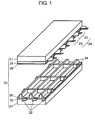
- Fig. 1 is an exploded perspective view of panel 10 according to a first embodiment of the present invention.
- Panel 10 includes front substrate 21 made of glass. Front substrate 21 is provided thereon with a plurality of display electrode pairs 24 each consisting of scan electrode 22 and sustain electrode 23, and further with dielectric layer 25 and protective layer 26 arranged in this order to cover scan electrodes 22 and sustain electrodes 23.
- protective layer 26 is made of a material based on MgO, which is field proven as material for the panels and has a large secondary electron emission coefficient and excellent durability when the discharge space is filled with the mixed gas of neon (Ne) and xenon (Xe).
- Panel 10 further includes rear substrate 31.
- Rear substrate 31 is provided thereon with data electrodes 32, dielectric layer 33 covering data electrodes 32, and barrier ribs 34 arranged further thereon in a parallel cross pattern.
- the side surfaces of barrier ribs 34 and the surface of dielectric layer 33 are covered with phosphor layers 35 of red (R), green (G), and blue (B).
- Front substrate 21 and rear substrate 31 face each other in such a manner that display electrode pairs 24 and data electrodes 32 intersect with each other with a small discharge space interposed therebetween.
- Front substrate 21 and rear substrate 31 are sealed by a sealing member such as a glass frit at their periphery.
- the discharge space is filled with, for example, a mixed gas of neon and xenon as a discharge gas.
- the discharge gas has a xenon partial pressure of about 10% in order to have a high luminance.
- the discharge space is partitioned into a plurality of sections by barrier rib 34 so as to form discharge cells at the intersections of display electrode pairs 24 and data electrodes 32. These discharge cells perform a discharge to generate illumination, thereby achieving image display.
- the structure of panel 10 is not limited to that described above.
- the barrier ribs may be formed in a stripe pattern.
- the proportions of the components in the discharge gas are not limited to that described above, either.
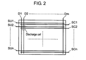
- Fig. 2 is an electrode array of panel 10 according to the first embodiment of the present invention.
- Panel 10 includes n scan electrodes SC1 to SCn (scan electrodes 22 of Fig. 1 ) and n sustain electrodes SU1 to SUn (sustain electrodes 23 of Fig. 1 ) extending in the row direction, and m data electrodes D1 to Dm (data electrodes 32 of Fig. 1 ) extending in the column direction.
- the plasma display device performs gradation display by a sub-field method.
- one field period is divided into a plurality of sub-fields and the on-off of illumination in each discharge cell is controlled sub-field by sub-field.
- Each sub-field includes an initializing period, an address period, and a sustain period.
- an initializing discharge is generated so that a wall charge necessary for a subsequent address discharge is formed on each electrode.
- the initializing operation is classified into an all-cell initializing operation to generate an initializing discharge in all discharge cells and a selective initializing operation to generate an initializing discharge only in the discharge cells that have performed a sustain discharge in the immediately preceding sub-field.
- an address discharge is generated to form wall charges selectively only in the discharge cells in which to generate illumination in the subsequent sustain period.
- sustain pulses whose number is in proportion to the luminance weight are applied alternately to scan electrodes 22 and sustain electrodes 23 of display electrode pairs 24. Consequently, a sustain discharge is generated in the discharge cells that have generated an address discharge so as to generate illumination in the discharge cells.
- the constant of proportionality in this case is called "luminance ratio".
- one field is divided into ten sub-fields (lst SF, 2nd SF, ⁇ , 10th SF), and these sub-fields have luminance weights of, for example, (1, 2, 3, 6, 11, 18, 30, 44, 60, and 80), respectively.
- the initializing period of the lst SF the all-cell initializing operation is performed, whereas in the initializing period of each of the 2nd to the 10th SF, the selective initializing operation is performed.
- display electrode pairs 24 are applied with sustain pulses whose number is determined by multiplying the luminance weight of each sub-field by a predetermined luminance ratio.
- the present embodiment is not limited to the aforementioned number of the sub-fields or the luminance weight of each sub-field, and may switch sub-field structures based on the image signal or the like.
- the minimum voltage of the gradually decreasing ramp waveform voltage to be applied to scan electrodes SC1 to SCn in the initializing period is controlled according to the accumulated time during which panel 10 is applied with current.
- the accumulated time is measured by an accumulated-time-measurement-circuit which is described later. More specifically, after the current accumulated time of panel 10 exceeds a predetermined time, the minimum voltage of the gradually decreasing ramp waveform voltage is set to the lowest voltage level in the initializing period of every sub-field.
- a stable address discharge can be generated without increasing the voltage required to generate an address discharge.
- the following is the outline of the driving voltage waveforms and their differences between when the current accumulated time measured by the accumulated-time-measurement-circuit is equal to or less than a predetermined time and after the current accumulated time exceeds the predetermined time.
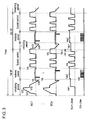
- Fig. 3 shows driving voltage waveforms to be applied to the electrodes of panel 10 of the first embodiment of the present invention.
- Fig. 3 includes the driving voltage waveforms in two sub-fields. One is a sub-field in which to perform an all-cell initializing operation (hereinafter, referred to as "all-cell initializing sub-field”), and the other is a sub-field in which to perform a selective initializing operation (hereinafter, referred to as "selective initializing sub-field"). The remaining sub-fields have driving voltage waveforms nearly the same as these.
- data electrodes D1 to Dm and sustain electrodes SU1 to SUn are applied with 0V.
- Scan electrodes SC1 to SCn are applied with a ramp waveform voltage gradually increasing (hereinafter, referred to as "up ramp waveform voltage") from voltage Vi1 to voltage Vi2, which exceeds the starting voltage.
- up ramp waveform voltage a ramp waveform voltage gradually increasing (hereinafter, referred to as "up ramp waveform voltage") from voltage Vi1 to voltage Vi2, which exceeds the starting voltage.
- the voltage difference between scan electrodes SC1 to SCn and sustain electrodes SU1 to SUn is equal to or less than the starting voltage.
- a weak initializing discharge continues between scan electrodes SC1 to SCn and sustain electrodes SU1 to SUn and between scan electrodes SC1 to SCn and data electrodes D1 to Dm. Consequently, a negative wall voltage is accumulated on scan electrodes SC1 to SCn, whereas a positive wall voltage is accumulated on data electrodes D1 to Dm and on sustain electrodes SU1 to SUn.
- the wall voltage on electrodes indicates the voltage generated by wall charges accumulated on the dielectric layers, protective layer, and phosphor layers covering these electrodes.
- sustain electrodes SU1 to SUn are applied with positive voltage Ve1.
- Data electrodes D1 to Dm are applied with 0V.
- Scan electrodes SC1 to SCn are applied with a ramp waveform voltage gradually decreasing (hereinafter, referred to as "down ramp waveform voltage") from voltage Vi3 to voltage Vi4, which exceeds the starting voltage.
- the voltage difference between scan electrodes SC1 to SCn and sustain electrodes SU1 to SUn is equal to or less than the starting voltage.
- the minimum voltage of the down ramp waveform voltage to be applied to scan electrodes SC1 to SCn is referred to as "initialization voltage Vi4".
- a weak initializing discharge continues between scan electrodes SC1 to SCn and sustain electrodes SU1 to SUn and between scan electrodes SC1 to SCn and data electrodes D1 to Dm. This reduces the negative wall voltage on scan electrodes SC1 to SCn and the positive wall voltage on sustain electrodes SU1 to SUn.
- the positive wall voltage on data electrodes D1 to Dm is adjusted to a value suitable for an address operation. As a result, the all-cell initializing operation to generate an initializing discharge in all discharge cells is complete.
- panel 10 is driven by switching initialization voltage Vi4 between two voltage levels.
- the high voltage level is referred to as Vi4H
- the low voltage level is referred to as Vi4L.
- initialization is performed using a down ramp waveform voltage having initialization voltage Vi4 set to Vi4L in the initializing period of every sub-field. This configuration is described in detail later. This makes it possible to generate a stable address discharge without increasing address pulse voltage Vd when the current accumulated time has increased.
- sustain electrodes SU1 to SUn are applied with voltage Ve2
- scan electrodes SC1 to SCn are applied with voltage Vc.
- negative scan pulse voltage Va is applied to scan electrode SC1 in the first row.
- the voltage difference at the intersection of data electrode Dk and scan electrode SC1 exceeds the starting voltage. This is because the voltage difference is equal to the sum of the difference between the voltages (Vd - Va) applied from the outside and the difference between the wall voltage on data electrode Dk and the wall voltage on scan electrode SC1.
- This generates an address discharge between data electrode Dk and scan electrode SC1 and between sustain electrode SU1 and scan electrode SC1, thereby accumulating a positive wall voltage on scan electrode SC1 and a negative wall voltage on sustain electrode SU1 and on data electrode Dk.
- an address discharge is generated in the discharge cells in which to generate illumination in the first row, thereby performing an address operation to accumulate a wall voltage on each electrode.
- the voltage difference at the intersections of those of data electrodes D1 to Dm that have not been applied with address pulse voltage Vd and scan electrode SC1 does not exceed the starting voltage. Therefore, no address discharge is generated in the corresponding discharge cells.
- the address operation is performed to reach the discharge cells in the n-th row so as to complete the address period.
- scan electrodes SC1 to SCn are applied with positive sustain pulse voltage Vs, and sustain electrodes SU1 to SUn are applied with 0V.
- the difference between the voltage on scan electrode SCi and the voltage on sustain electrode SUi exceeds the starting voltage. This is because the voltage difference is equal to the sum of sustain pulse voltage Vs and the difference between the wall voltage on scan electrode SCi and the wall voltage on sustain electrode SUi.
- sustain electrodes SU1 to SUn are applied with sustain pulse voltage Vs.
- the difference between the voltage on sustain electrode SUi and the voltage on scan electrode SCi exceeds the starting voltage.
- This generates another sustain discharge between sustain electrode SUi and scan electrode SCi, thereby accumulating a negative wall voltage on sustain electrode SUi and a positive wall voltage on scan electrode SCi.
- sustain pulses whose number is determined by multiplying the luminance weight by the luminance ratio are applied alternately to scan electrodes SC1 to SCn and sustain electrodes SU1 to SUn so as to provide a potential difference between the electrodes of display electrode pairs 24.
- a sustain discharge is continued in the discharge cells that have generated an address discharge in the address period.
- a voltage difference is applied in the form of a small-width pulse between scan electrodes SC1 to SCn and sustain electrodes SU1 to SUn so as to erase the wall voltage on scan electrode SCi and on sustain electrode SUi with the positive wall voltage left on data electrode Dk.
- this discharge is referred to as "erase discharge”.
- sustain electrodes SU1 to SUn are applied with voltage Ve1 to reduce the potential difference between the electrodes of display electrode pairs 24. As a result, the sustain operation in the sustain period is complete.
- scan electrodes SC1 to SCn are applied with a down ramp waveform voltage gradually decreasing from voltage Vi3' to initialization voltage Vi4, while sustain electrodes SU1 to SUn are maintained at voltage Ve1 and data electrodes D1 to Dm are maintained at 0V.
- the discharge cells that have not generated a sustain discharge in the preceding sub-field do not generate a discharge and maintain the wall charge at the level of the end of the initializing period of the preceding sub-field.
- an initializing discharge is selectively performed only in the discharge cells that have performed a sustain operation in the sustain period of the immediately preceding sub-field.
- initialization voltage Vi4 is switched between high voltage level Vi4H and low voltage level Vi4L in the same manner as the down ramp waveform voltage in the all-cell initializing operation.
- the operation in the subsequent address period is not described because it is the same as in the address period of the all-cell initializing sub-field.
- the operation in the subsequent sustain period is also the same except for the number of the sustain pulses.
- the operation in the initializing period of each of the 3rd to the 10th SF is the same selective initializing operation as in the 2nd SF.
- the address operation in the address period is also the same as in the 2nd SF, and the operation in the sustain period is also the same except for the number of the sustain pulses.
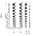
- Fig. 4 shows a sub-field structure of a plasma display device according to the first embodiment of the present invention.
- the driving waveforms within one field are shown in a simplified manner, but identical in each sub-field to the driving voltage waveforms of Fig. 3 .
- Fig. 4 shows the sub-field structure of the present embodiment where one field is divided into ten sub-fields (lst SF, 2nd SF, ⁇ , 10th SF), and these sub-fields have luminance weights of (1, 2, 3, 6, 11, 18, 30, 44, 60, and 80), respectively.
- the lst SF is an all-cell initializing sub-field
- the 2nd to the 10th SF are selective initializing sub-fields.
- display electrode pairs 24 are applied with sustain pulses whose number is determined by multiplying the luminance weight of each sub-field by a predetermined luminance ratio.
- the down ramp waveform voltage of the driving voltage waveform to be applied to scan electrodes SC1 to SCn is changed depending on the current accumulated time of panel 10. The detail is described as follows with reference to Fig. 5A, 5B
- Fig. 5A, 5B shows driving voltage waveforms to be applied to scan electrodes SC1 to SCn according to the first embodiment of the present invention.
- Fig. 5A shows a waveform when the current accumulated time of panel 10 measured by the accumulated-time-measurement-circuit is equal to or less than a predetermined time (500 hours or less in the present embodiment).
- Fig. 5B shows a waveform after the current accumulated time exceeds the predetermined time (over 500 hours in the present embodiment).
- the down ramp waveform voltage is generated by switching initialization voltage Vi4, which is the minimum voltage of the down ramp waveform voltage, between two voltage levels: high voltage level Vi4H and low voltage level Vi4L.
- the voltage level of initialization voltage Vi4 is switched between Vi4L and Vi4H depending on whether the current accumulated time of panel 10 measured by the after-mentioned accumulated-time-measurement-circuit has exceeded the predetermined time or not.
- an initialization is performed by generating a down ramp waveform voltage having initialization voltage Vi4 set to Vi4H in the initializing period of every sub-field.
- an initialization is performed by generating a down ramp waveform voltage having initialization voltage Vi4 set to Vi4L in the initializing period of every sub-field.
- the discharge characteristics change depending on the current accumulated time of panel 10.
- factors to make the discharge unstable such as a discharge delay and a dark current also change depending on the current accumulated time of panel 10.
- the discharge delay indicates the time after a voltage to generate a discharge is applied to discharge cells and until the generation of a discharge.
- the dark current indicates a current generated in a discharge cell independently of discharge. As a result, the applied voltage required to generate a stable address discharge also changes depending on the current accumulated time of panel 10.
- Fig. 6 shows the relation between the current accumulated time of the panel and address pulse voltage Vd necessary for the generation of a stable address discharge in the first embodiment of the present invention.
- the vertical axis represents address pulse voltage Vd required to generate a stable address discharge
- the horizontal axis represents the current accumulated time of panel 10.
- address pulse voltage Vd required is about 60V.
- address pulse voltage Vd required is about 73V, which is higher by about 13V. After the current accumulated time has reached about 1000 hours, address pulse voltage Vd required stays around 75V.
- an initializing discharge is generated by applying a down ramp waveform voltage to scan electrodes SC1 to SCn.
- the state of the wall charge formed on each electrode changes depending on the voltage level of initialization voltage Vi4 which is the minimum voltage of the down ramp waveform voltage.
- the applied voltage necessary for the subsequent address discharge changes in the same manner.
- the initialization voltage Vi4 and the applied voltage have the following relation.
- Fig. 7 shows the relation between initialization voltage Vi4 and address pulse voltage Vd necessary for the generation of the stable address discharge in the first embodiment of the present invention.
- the vertical axis represents address pulse voltage Vd required to generate a stable address discharge
- the horizontal axis represents initialization voltage Vi4.
- address pulse voltage Vd required to generate a stable address discharge changes depending on the level of initialization voltage Vi4. As initialization voltage Vi4 decreases, address pulse voltage Vd required to generate a stable address discharge also decreases. For example, when initialization voltage Vi4 is about -90V, address pulse voltage Vd is about 66V. When initialization voltage Vi4 is about -95V, address pulse voltage Vd is about 50V. Thus, when initialization voltage Vi4 is decreased from about -90V to about -95V, address pulse voltage Vd required to generate a stable address discharge decreases by about 16V.
- address pulse voltage Vd required to generate a stable address discharge increases as the current accumulated time increases, and decreases as initialization voltage Vi4 decreases. More specifically, an increase in the current accumulated time causes an increase in address pulse voltage Vd required to generate a stable address discharge, but the increase in address pulse voltage Vd can be compensated by decreasing initialization voltage Vi4 depending on the current accumulated time. As a result, a stable address discharge can be generated without increasing address pulse voltage Vd.
- the after-mentioned accumulated-time-measurement-circuit measures the current accumulated time of panel 10.
- the down ramp waveform voltage is generated with initialization voltage Vi4 set to Vi4H as shown in Fig. 5A .
- the down ramp waveform voltage is generated with initialization voltage Vi4 set to Vi4L, which is lower than Vi4H as shown in Fig. 5B . This achieves a stable address operation without increasing address pulse voltage Vd required to generate a stable address discharge.
- Vi4L is set to -95V
- Vi4H is set to -90V, which is higher by 5V than Vi4L.
- This experiment is applied to a 50 inch panel having 1080 display electrode pairs.
- the aforementioned values are based on this panel, so that the present embodiment is not limited to these values.
- Fig. 8 is a circuit block diagram of the plasma display device according to the first embodiment of the present invention.
- Plasma display device 1 includes panel 10, image-signal-processing-circuit 41, data-electrode-driving-circuit 42, scan-electrode-driving-circuit 43, sustain-electrode-driving-circuit 44, timing-generating-circuit 45, accumulated-time-measurement-circuit 48, and a power supply circuit (unillustrated), which supplies each circuit block with necessary power.
- Image-signal-processing-circuit 41 converts a received image signal "sig" into image data indicating the on-off of illumination in each sub-field.
- Data-electrode-driving-circuit 42 converts the image data in each sub-field into signals corresponding to data electrodes D1 to Dm so as to drive data electrodes D1 to Dm.
- Accumulated-time-measurement-circuit 48 includes well-known timer 81 for increasing the value by a constant amount at regular time intervals while panel 10 is applied with current. In timer 81, the elapsed time is accumulated without resetting so as to measure the accumulated time during which panel 10 is applied with current. Then, accumulated-time-measurement-circuit 48 compares the current accumulated time of panel 10 measured by timer 81 with a predetermined threshold value so as to determine whether the current accumulated time of panel 10 has exceeded the predetermined time or not. Accumulated-time-measurement-circuit 48 then outputs a signal indicating the determined result to timing-generating-circuit 45.
- the threshold value is set to 500 hours, but is not limited to this value. It is preferably set to a value determined according to the characteristics of the panel, the specification of the plasma display device, or the like.
- Timing-generating-circuit 45 generates various timing signals to control the operations of these circuit blocks, and outputs them to the circuit blocks. Timing-generating-circuit 45 generates the timing signals based on a horizontal synchronizing signal H, a vertical synchronizing signal V, and the current accumulated time of panel 10 measured by accumulated-time-measurement-circuit 48. As described above, in the present embodiment, initialization voltage Vi4 of the down ramp waveform voltage to be applied to scan electrodes SC1 to SCn in the initializing period is controlled based on the current accumulated time. Timing-generating-circuit 45 outputs a timing signal corresponding to the current accumulated time to scan-electrode-driving-circuit 43. As a result, the stabilization of a address operation is controlled.
- Scan-electrode-driving-circuit 43 includes an initialization-waveform-generating-circuit, a sustain-pulse-generating-circuit, and a scan-pulse-generating-circuit.
- the initialization-waveform-generating-circuit generates an initializing waveform voltage to be applied to scan electrodes SC1 to SCn in the initializing period.
- the sustain-pulse-generating-circuit generates a sustain pulse voltage to be applied to scan electrodes SC1 to SCn in the sustain period.
- the scan-pulse-generating-circuit generates a scan pulse voltage to be applied to scan electrodes SC1 to SCn in the address period.
- Scan-electrode-driving-circuit 43 drives scan electrodes SC1 to SCn based on the timing signal.
- Sustain-electrode-driving-circuit 44 includes a sustain-pulse-generating-circuit and a circuit for generating voltages Ve1 and Ve2, and drives sustain electrodes SU1 to SUn based on the timing signal.
- Fig. 9 is a circuit diagram of scan-electrode-driving-circuit 43 in the first embodiment of the present invention.
- Scan-electrode-driving-circuit 43 includes sustain-pulse-generating-circuit 50 for generating the sustain pulse voltage, initialization-waveform-generating-circuit 53 for generating the initializing waveform voltage, and scan-pulse-generating-circuit 54 for generating the scan pulse voltage.
- Sustain-pulse-generating-circuit 50 includes power-recovery-circuit 51 and clamp circuit 52.
- Power-recovery-circuit 51 includes capacitor C1 for power recovery, switching elements Q1 and Q2, diodes D1 and D2 for backflow prevention, and inductor L1 for resonance.
- Capacitor C1 for power recovery has a much larger capacity than interelectrode capacitance Cp, and is charged with Vs/2, which is about half voltage Vs so as to function as the power of power-recovery-circuit 51.
- Clamp circuit 52 includes switching element Q3 for clamping scan electrodes SC1 to SCn to voltage Vs, and switching element Q4 for clamping scan electrodes SC1 to SCn to 0V.
- Sustain-pulse-generating-circuit 50 generates sustain pulse voltage Vs based on the timing signal from timing-generating-circuit 45.
- switching element Q1 when a sustain pulse is raised, switching element Q1 is turned on to make interelectrode capacitance Cp resonate with inductor L1, so that power is supplied from capacitor C1 for power recovery to scan electrodes SC1 to SCn via switching element Q1, diode D1, and inductor L1.
- switching element Q3 When the voltage of scan electrodes SC1 to SCn approaches Vs, switching element Q3 is turned on to clamp scan electrodes SC1 to SCn to voltage Vs.
- switching element Q2 when the sustain pulse is lowered, switching element Q2 is turned on to make interelectrode capacitance Cp resonate with inductor L1, so that power is recovered from interelectrode capacitance Cp to capacitor C1 for power recovery via inductor L1, diode D2, and switching element Q2.
- switching element Q4 When the voltage of scan electrodes SC1 to SCn approaches 0V, switching element Q4 is turned on to clamp scan electrodes SC1 to SCn to 0V.
- Initialization-waveform-generating-circuit 53 includes two Miller integrator circuits, and two separation circuits.
- One of the Miller integrator circuits includes switching element Q11, capacitor C10, and resistor R10, and generates an up ramp waveform voltage gradually increasing to reach voltage Vi2.
- the other Miller integrator circuit includes switching element Q14, capacitor C12, and resistor R11, and generates a down ramp waveform voltage gradually decreasing to reach initialization voltage Vi4.
- One of the separation circuits uses switching element Q12, and the other separation circuit uses switching element Q13.
- Initialization-waveform-generating-circuit 53 generates the aforementioned initializing waveform voltage based on the timing signal from timing-generating-circuit 45, and controls initialization voltage Vi4 in an all-cell initializing operation.
- the input terminals of the Miller integrator circuits are shown as input terminals INa and INb.
- input terminal INa When an up ramp waveform voltage of the initializing waveform voltage is generated, input terminal INa is applied with a predetermined voltage (for example, 15V) so as to set input terminal INa to "Hi". As a result, a constant current flows from resistor R10 toward capacitor C10 so as to increase the source voltage of switching element Q11 in a ramp fashion, making the output voltage of scan-electrode-driving-circuit 43 begin to increase in a ramp fashion.
- a predetermined voltage for example, 15V
- Scan-pulse-generating-circuit 54 includes switch circuits OUT1 to OUTn, switching element Q21, control circuits IC1 to ICn, diode D21, and capacitor C21.
- Switch circuits OUT1 to OUTn output a scan pulse voltage to scan electrodes SC1 to SCn.
- Switching element Q21 clamps the low voltage side of switch circuits OUT1 to OUTn to voltage Va.
- Control circuits IC1 to ICn control switch circuits OUT1 to OUTn, respectively.
- Diode D21 applies voltage Vc to the high voltage side of switch circuits OUT1 to OUTn, voltage Vc being obtained by superimposing voltage Vscn on voltage Va.
- Switch circuits OUT1 to OUTn include switching elements QH1 to QHn, respectively, for outputting voltage Vc and switching elements QL1 to QLn, respectively, for outputting voltage Va.
- Scan-pulse-generating-circuit 54 generates scan pulse voltage Va to be applied sequentially to scan electrodes SC1 to SCn in the address period based on the timing signal from timing-generating-circuit 45.
- Scan-pulse-generating-circuit 54 outputs the voltage waveform of initialization-waveform-generating-circuit 53 in the initializing period without any change and also outputs the voltage waveform of sustain-pulse-generating-circuit 50 in the sustain period without any change.
- switching elements Q3, Q4, Q12, and Q13 are each formed of parallel-connected FETs or parallel-connected IGBTs to reduce the impedance.
- Scan-pulse-generating-circuit 54 includes AND gate AG for performing a logical AND operation, and comparator CP for comparing the size of input signals inputted to two input terminals. More specifically, comparator CP compares voltage (Va + Vset2) obtained by superimposing voltage Vset2 on voltage Va with the driving waveform voltage. Comparator CP then outputs "0" when the driving waveform voltage is higher than voltage (Va + Vset2); otherwise outputs "1".
- AND gate AG receives two input signals, that is, output signal (CEL1.) of comparator CP and switching signal CEL2. Switching signal CEL2 can be, for example, the timing signal from timing-generating-circuit 45. AND gate AG outputs "1" when both input signals are “1”; otherwise outputs "0".
- Scan-pulse-generating-circuit 54 outputs a driving waveform voltage via switching elements QL1 to QLn when the output of AND gate AG is "0", and outputs voltage Vc obtained by superimposing voltage Vscn on voltage Va via switching elements QH1 to QHn when the output of AND gate AG is "1".
- the sustain-pulse-generating-circuit of sustain-electrode-driving-circuit 44 has the same structure as sustain-pulse-generating-circuit 50.
- the sustain-pulse-generating-circuit includes a power-recovery-circuit and two switching elements.
- the power-recovery-circuit recovers the power used to drive sustain electrodes SU1 to SUn for recycling.
- One of the two switching elements clamps sustain electrodes SU1 to SUn to voltage Vs and the other clamps sustain electrodes SU1 to SUn to 0V.
- the sustain-pulse-generating-circuit generates sustain pulse voltage Vs.
- the Miller integrator circuits are formed of FETs which are practical and have a comparatively simple structure.
- the Miller integrator circuits may be replaced by other circuits as long as they can generate an up ramp waveform voltage and a down ramp waveform voltage.
- initialization-waveform-generating-circuit 53 and a method for controlling initialization voltage Vi4 are described as follows with reference to drawings.
- the operation of setting initialization voltage Vi4 to Vi4L is described with reference to Fig. 10 first, and then the operation of setting initialization voltage Vi4 to Vi4H is described with reference to Fig. 11 .
- the method for controlling initialization voltage Vi4 is described by showing the driving waveforms in an all-cell initializing operation; however, initialization voltage Vi4 can be controlled in the same manner in a selective initializing operation.
- each driving voltage waveform is divided into five periods: periods T1 to T5 in an all-cell initializing operation. These periods are described as follows. The following description is on the assumption that voltages Vi1 and Vi3 are equal to voltage Vs; voltage Vi2 is equal to voltage Vr; voltage Vi4L is equal to negative voltage Va; and voltage Vi4H is equal to voltage (Va + Vset2) which is obtained by superimposing voltage Vset2 on negative voltage Va. As a result, voltage Vi4H is higher than scan pulse voltage Va in the address period, and voltage Vi4L is equal to scan pulse voltage Va.
- the operations of activating and deactivating the switching elements are referred to as "ON" and "OFF", respectively.
- signals to switch the switching elements ON and OFF are referred to as “Hi” and “Lo”, respectively.
- Input signals CEL1 and CEL2 to be inputted to AND gate AG are also each referred to as “Hi” when it is “1”, and referred to "Lo” when it is “0".
- Fig. 10 is a timing chart showing an example of the operation of scan-electrode-driving-circuit 43 in an all-cell initializing period in the first embodiment of the present invention.
- Switching signal CEL2 is maintained at "0" in periods T1 to T5 so that initialization voltage Vi4 can be set to Vi4L.
- Scan-pulse-generating-circuit 54 outputs a signal to be inputted to switching elements QL1 to QLn, that is, the voltage waveform of initialization-waveform-generating-circuit 53 without any change.
- Switching element Q1 of sustain-pulse-generating-circuit 50 is turned to the ON position. This makes interelectrode capacitance Cp resonate with inductor L1, so that the voltage to be applied from capacitor C1 for power recovery to scan electrodes SC1 to SCn via switching element Q1, diode D1, and inductor L1 starts to increase.
- Switching element Q3 of sustain-pulse-generating-circuit 50 is turned to the ON position. This allows voltage Vs to be applied to scan electrodes SC1 to SCn via switching element Q3, so that the potential of scan electrodes SC1 to SCn becomes voltage Vs (which is equal to voltage Vi1 in the present embodiment).
- Input terminal INa of the Miller integrator circuit generating an up ramp waveform voltage is set to "Hi". More specifically, input terminal INa is applied with a voltage of, for example, 15V As a result, a constant current flows from resistor R10 toward capacitor C10 so as to increase the source voltage of switching element Q11 in a ramp fashion, making the output voltage of scan-electrode-driving-circuit 43 begin to increase in a ramp fashion. This voltage increase is continued while input terminal INa is "Hi".
- input terminal INa When the output voltage increases to reach voltage Vr (which is equal to voltage Vi2 in the present embodiment), input terminal INa is set to "Lo". More specifically, input terminal INa is applied with a voltage of, for example, 0V.
- scan electrodes SC1 to SCn are applied with an up ramp waveform voltage gradually increasing from voltage Vs, which is equal to or less than the starting voltage to voltage Vr, which exceeds the starting voltage.
- voltage Vs is equal to voltage Vi1
- voltage Vr is equal to voltage Vi2.
- Input terminal INb of the Miller integrator circuit generating a down ramp waveform voltage is set to "Hi". More specifically, input terminal INb is applied with a voltage of, for example, 15V. As a result, a constant current flows from resistor R11 toward capacitor C12 so as to decrease the drain voltage of switching element Q14 in a ramp fashion, making the output voltage of scan-electrode-driving-circuit 43 begin to decrease in a ramp fashion. After the output voltage has reached predetermined negative voltage Vi4L, input terminal INb is set to "Lo". More specifically, input terminal INb is applied with a voltage of, for example, 0V.
- comparator CP compares the down ramp waveform voltage with voltage (Va + Vset2) obtained by superimposing voltage Vset2 on voltage Va.
- the output signal of comparator CP is switched from “0" to "1” at time t5 when the down ramp waveform voltage becomes equal to or less than voltage (Va + Vset2).
- switching signal CEL2 is maintained at “0”, so that AND gate AG outputs "0". Therefore, scan-pulse-generating-circuit 54 outputs a down ramp waveform voltage having initialization voltage Vi4 set to negative voltage Va, that is, Vi4L without any change.
- Vi4L is made equal to negative voltage Va. Therefore, after the down ramp waveform voltage has reached Vi4L, the voltage is maintained for a certain period of time in Fig. 10 .
- this waveform is generated under the influence of the circuit configuration of Fig. 9 , and the present embodiment is not limited to this waveform or the circuit configuration of Fig. 9 .
- the down ramp waveform voltage may be switched to voltage Vc immediately after it has reached Vi4L.
- scan electrodes SC1 to SCn are applied with an up ramp waveform voltage gradually increasing from voltage Vi1 which is equal to or less than the starting voltage to voltage Vi2 which exceeds the starting voltage. After this, scan electrodes SC1 to SCn are applied with a down ramp waveform voltage gradually decreasing from voltage Vi3 to initialization voltage Vi4L.
- Fig. 11 is a timing chart showing another example of the operation of scan-electrode-driving-circuit 43 in an all-cell initializing period in the first embodiment of the present invention.
- Switching signal CEL2 is maintained at "1" in periods T1 to T5' so that initialization voltage Vi4 can be set to Vi4H. Since the operation in periods T1 to T4 of Fig. 11 is equal to that in periods T1 to T4 of Fig. 10 , the following description is focused on the operation in period T5', which is different from period T5 of Fig. 10 .
- input terminal INb of the Miller integrator circuit generating a down ramp waveform voltage is set to "Hi". More specifically, input terminal INb is applied with a voltage of, for example, 15V. As a result, a constant current flows from resistor R11 toward capacitor C12 so as to decrease the drain voltage of switching element Q14 in a ramp fashion, making the output voltage of scan-electrode-driving-circuit 43 begin to decrease in a ramp fashion.
- comparator CP compares the down ramp waveform voltage with voltage (Va + Vset2) obtained by superimposing voltage Vset2 on voltage Va.
- the output signal of comparator CP is switched from “0" to "1” at time t5 when the down ramp waveform voltage becomes equal to or less than voltage (Va + Vset2).
- switching signal CEL2 is at "1", so that AND gate AG receives inputs which are both “1", and then outputs "1". Consequently, scan-pulse-generating-circuit 54 outputs voltage Vc obtained by superimposing voltage Vscn on negative voltage Va.
- the minimum voltage of the down ramp waveform voltage can be (Va + Vset2), that is, Vi4H.
- Input terminal INb is set at "Lo" between when the output of scan-pulse-generating-circuit 54 becomes voltage Vc, and until the initializing period is over.
- the down ramp waveform voltage is switched to voltage Vc immediately after having reached Vi4H in Fig. 11 .
- the present embodiment is not limited to this waveform; after the down ramp waveform voltage has reached Vi4H, the voltage may be maintained for a certain period of time.
- scan-electrode-driving-circuit 43 has the circuit configuration of Fig. 9 .
- the minimum voltage of the gradually decreasing down ramp waveform voltage that is, initialization voltage Vi4
- initialization voltage Vi4 can be easily controlled just by setting voltage Vset2 to a desired voltage level.
- the present embodiment describes the control of initialization voltage Vi4 in an all-cell initializing operation; however, the control can be performed in the same manner in a selective initializing operation except that an up ramp waveform voltage is not generated although a down ramp waveform voltage is generated.
- Initialization voltage Vi4 may be changed by other methods.
- voltage Vi4 may be increased or decreased by controlling the inclination of the ramp decreasing from voltage Vi3 to voltage Vi4.
- the method for changing initialization voltage Vi4 in the present embodiment is not limited to the aforementioned one.
- Vset2 is set to 5V so as to make Vi4H higher than Vi4L by 5V; however, Vset2 is not limited to this voltage and can preferably be set to a value determined according to the characteristics of the panel, the specification of the plasma display device, or the like.
- initialization voltage Vi4 is switched between Vi4H and Vi4L, which is lower than Vi4H, and initialization voltage Vi4 is changed depending on the current accumulated time of panel 10.
- the down ramp waveform voltage is generated with initialization voltage Vi4 set to Vi4H.
- the down ramp waveform voltage is generated with initialization voltage Vi4 set to Vi4L, which is lower than Vi4H. This achieves a stable address operation without increasing address pulse voltage Vd when the current accumulated time has increased.
- the down ramp waveform voltage in the initializing period of every sub-field, is generated with initialization voltage Vi4 set to Vi4H as shown in Fig. 5A when the current accumulated time is equal to or less than the predetermined time.
- the down ramp waveform voltage is generated with initialization voltage Vi4 set to Vi4L as shown in Fig. 5B after the current accumulated time exceeds the predetermined time.
- the sub-field structure of the present invention is not limited to this.
- Fig. 12A shows an example of a sub-field structure according to a second embodiment of the present invention
- Fig. 12B shows another example of the sub-field structure.
- the second embodiment differs from the first embodiment only in the sub-field structure and is identical in the structure and operation of each circuit, each driving waveform, and the like.
- the present embodiment may have a structure having a sub-field in which the down ramp waveform voltage is generated with initialization voltage Vi4 set to Vi4L when the current accumulated time is equal to or less than a predetermined time.
- the down ramp waveform voltage is generated with initialization voltage Vi4 set to Vi4H in the initializing period of each of the 1st SF and the 5th to the 10th SF, and is generated with initialization voltage Vi4 set to Vi4L in the initializing period of each of the 2nd to the 4th SF.
- the present embodiment may have another structure having a sub-field in which the down ramp waveform voltage is generated with initialization voltage Vi4 set to Vi4H after the current accumulated time exceeds the predetermined time.
- the down ramp waveform voltage is generated with initialization voltage Vi4 set to Vi4L in the initializing period of each of the lst to the 9th SF, and is generated with initialization voltage Vi4 set to Vi4H in the initializing period of the 10th SF.
- the ratio of the sub-fields in which the down ramp waveform voltage is generated with initialization voltage Vi4 set to Vi4Li in one field period should be larger after the current accumulated time exceeds the predetermined time than when the current accumulated time is equal to or less than the predetermined time. This achieves the same effect as described above.
- Vset2 is set to 5V
- initialization voltage Vi4 is switched between Vi4L and Vi4H, which is higher than Vi4L by 5V.
- the potential of Vi4L is set to equal to negative voltage Va.
- the potential difference between Vi4L and Vi4H, and the potential of ViL are not limited to these values, but can be set to values determined according to the characteristics of the panel, the specification of the plasma display device, or the like.
- initialization voltage Vi4 is switched between two voltage levels: Vi4L and Vi4H, but may alternatively be switched between three or more voltage levels.
- Fig. 13A shows an example of a sub-field structure in the second embodiment of the present invention in which initialization voltage Vi4 has three voltage levels.
- Fig. 13B shows another example of the sub-field structure in the second embodiment of the present invention in which initialization voltage Vi4 has three voltage levels. It is possible to provide Vi4M between Vi4H and Vi4L. For example, Vi4H can be higher than Vi4L by 10V, and Vi4M can be higher than Vi4L by 5V.
- the down ramp waveform voltage is generated with initialization voltage Vi4 set to Vi4M when the current accumulated time is equal to or less than a predetermined time.
- the down ramp waveform voltage is generated with initialization voltage Vi4 set to Vi4M in the initializing period of each of the lst to the 5th SF, and is generated with initialization voltage Vi4 set to Vi4H in the initializing period of each of the 6th to the 10th SF.
- the down ramp waveform voltage is generated with initialization voltage Vi4 set to Vi4M after the current accumulated time exceeds the predetermined time. In the example shown in Fig.
- the down ramp waveform voltage is generated with initialization voltage Vi4 set to Vi4L equal to the scan pulse voltage in the initializing period of each of the lst to the 9th SF, and is generated with initialization voltage Vi4 set to Vi4M in the initializing period of the 10th SF.
- the ratio of the sub-fields in which the down ramp waveform voltage is generated with initialization voltage Vi4 set to the minimum voltage (in this case, Vi4L) in one field period should be larger after the current accumulated time exceeds the predetermined time than when the current accumulated time is equal to or less than the predetermined time. This achieves the same effect as described above.
- the predetermined time is set to 500 hours, and initialization voltage Vi4 is changed between when the current accumulated time is equal to or less than 500 hours and when it is over 500 hours.
- the predetermined time may be set to a value determined according to the characteristics of the panel, the specification of the plasma display device, or the like. For example, it is possible to provide a plurality of threshold values: 500 hours, 750 hours, and 1000 hours, and to gradually increase the ratio of the sub-fields in which the down ramp waveform voltage is generated with initialization voltage Vi4 set to Vi4L in one field period every time the current accumulated time exceeds a threshold value.
- initialization voltage Vi4 having a down ramp waveform is changed after the current accumulated time exceeds the predetermined time. It is alternatively possible that even after the current accumulated time exceeds the predetermined time, the driving waveform is maintained until the plasma display device is in a non-operating state, and then initialization voltage Vi4 is changed when the plasma display device is again put into operation. More specifically, even if accumulated-time-measurement-circuit 48 outputs a signal indicating that the current accumulated time has exceeded the predetermined time while plasma display device 1 is in operation, that is, while timing-generating-circuit 45 is in operation and outputting the timing signals to drive panel 10, timing-generating-circuit 45 continues to output the same timing signals to drive panel 10.
- timing-generating-circuit 45 outputs a timing signal to generate a down ramp waveform voltage with initialization voltage Vi4 set to Vi4L.
- This structure can prevent brightness fluctuations which may be caused by changing the initializing waveform voltage while plasma display device 1 is in operation, and can also increase the image display quality.
- the embodiments of the present invention do not limit the voltage values of Vi4L and Vi4H, the sub-fields in which to switch initialization voltage Vi4, the sub-field structure, and the like to the values described above. They are preferably set to values determined according to the characteristics of the panel, the specification of the plasma display device, or the like.
- the discharge gas has a xenon partial pressure of 10%.
- the driving voltage is determined in the same manner according to the panel.
- the other specific values used in the embodiments of the present invention are just examples, and are preferably set to values determined according to the characteristics of the panel, the specification of the plasma display device, or the like.
- the minimum voltage of a decreasing ramp waveform voltage generated in the initializing period is changed depending on the accumulated time during which the panel is supplied with current. This makes it possible for a panel having high luminance to generate a stable address discharge without increasing the voltage required to generate an address discharge when the current accumulated time of the panel has increased. As the result, the present invention is useful as a plasma display device having high image display quality, and as a method for driving the panel.
Landscapes
- Engineering & Computer Science (AREA)
- Physics & Mathematics (AREA)
- Power Engineering (AREA)
- Plasma & Fusion (AREA)
- Computer Hardware Design (AREA)
- General Physics & Mathematics (AREA)
- Theoretical Computer Science (AREA)
- Control Of Indicators Other Than Cathode Ray Tubes (AREA)
- Control Of Gas Discharge Display Tubes (AREA)
- Transforming Electric Information Into Light Information (AREA)
Applications Claiming Priority (2)
| Application Number | Priority Date | Filing Date | Title |
|---|---|---|---|
| JP2006335400 | 2006-12-13 | ||
| PCT/JP2007/072648 WO2008072458A1 (ja) | 2006-12-13 | 2007-11-22 | プラズマディスプレイ装置およびプラズマディスプレイパネルの駆動方法 |
Publications (3)
| Publication Number | Publication Date |
|---|---|
| EP2096622A1 EP2096622A1 (en) | 2009-09-02 |
| EP2096622A4 EP2096622A4 (en) | 2010-07-14 |
| EP2096622B1 true EP2096622B1 (en) | 2013-06-05 |
Family
ID=39511483
Family Applications (1)
| Application Number | Title | Priority Date | Filing Date |
|---|---|---|---|
| EP07832377.1A Not-in-force EP2096622B1 (en) | 2006-12-13 | 2007-11-22 | Plasma display device and method for driving plasma display panel |
Country Status (6)
| Country | Link |
|---|---|
| US (1) | US20090303222A1 (ja) |
| EP (1) | EP2096622B1 (ja) |
| JP (1) | JP5093105B2 (ja) |
| KR (1) | KR100961024B1 (ja) |
| CN (1) | CN101454819B (ja) |
| WO (1) | WO2008072458A1 (ja) |
Families Citing this family (2)
| Publication number | Priority date | Publication date | Assignee | Title |
|---|---|---|---|---|
| KR200458355Y1 (ko) * | 2010-07-16 | 2012-02-15 | 안수철 | 변신만화액자 |
| US10888090B2 (en) | 2015-06-30 | 2021-01-12 | King Abdullah University Of Science And Technology | Plant growth promoters and methods of using them |
Family Cites Families (17)
| Publication number | Priority date | Publication date | Assignee | Title |
|---|---|---|---|---|
| JPH0791514A (ja) * | 1990-12-14 | 1995-04-04 | Boris Borisovich Ropateikku | 回転運動から往復運動への、およびその逆の変換機構 |
| JP3733773B2 (ja) | 1999-02-22 | 2006-01-11 | 松下電器産業株式会社 | Ac型プラズマディスプレイパネルの駆動方法 |
| JP4669633B2 (ja) * | 2001-06-28 | 2011-04-13 | パナソニック株式会社 | ディスプレイパネルの駆動方法及びディスプレイパネルの駆動装置 |
| JP2003140601A (ja) * | 2001-11-06 | 2003-05-16 | Matsushita Electric Ind Co Ltd | プラズマディスプレイの駆動方法 |
| KR20050018032A (ko) * | 2003-08-12 | 2005-02-23 | 삼성에스디아이 주식회사 | 플라즈마 디스플레이 패널의 구동 방법 및 플라즈마 표시장치 |
| JP4819315B2 (ja) * | 2004-02-20 | 2011-11-24 | 日立プラズマディスプレイ株式会社 | プラズマディスプレイ及びその駆動方法 |
| US20060033680A1 (en) * | 2004-08-11 | 2006-02-16 | Lg Electronics Inc. | Plasma display apparatus including an energy recovery circuit |
| KR100610891B1 (ko) * | 2004-08-11 | 2006-08-10 | 엘지전자 주식회사 | 플라즈마 디스플레이 패널의 구동방법 |
| JP4873844B2 (ja) * | 2004-09-24 | 2012-02-08 | パナソニック株式会社 | プラズマディスプレイ装置 |
| JPWO2006132334A1 (ja) * | 2005-06-09 | 2009-01-08 | 松下電器産業株式会社 | プラズマディスプレイパネル装置の駆動方法およびプラズマディスプレイパネル装置 |
| US20070091514A1 (en) * | 2005-10-21 | 2007-04-26 | Hitachi Global Storage Technologies Netherlands B.V. | Magnetoresistive (MR) elements having improved hard bias seed layers |
| TW200733043A (en) * | 2006-02-06 | 2007-09-01 | Matsushita Electric Ind Co Ltd | Plasma display apparatus and driving method of plasma display panel |
| JP4811053B2 (ja) * | 2006-02-24 | 2011-11-09 | パナソニック株式会社 | プラズマディスプレイパネルの駆動方法およびプラズマディスプレイ装置 |
| KR101025673B1 (ko) * | 2006-02-24 | 2011-03-30 | 파나소닉 주식회사 | 플라즈마 디스플레이 패널의 구동 방법 및 플라즈마 디스플레이 장치 |
| KR100938313B1 (ko) * | 2006-02-28 | 2010-01-22 | 파나소닉 주식회사 | 플라즈마 디스플레이 패널의 구동 방법 및 플라즈마디스플레이 장치 |
| US8068069B2 (en) * | 2006-02-28 | 2011-11-29 | Panasonic Corporation | Method of driving plasma display panel and plasma display apparatus |
| WO2008081698A1 (ja) * | 2006-12-28 | 2008-07-10 | Panasonic Corporation | プラズマディスプレイ装置およびプラズマディスプレイパネルの駆動方法 |
-
2007
- 2007-11-22 EP EP07832377.1A patent/EP2096622B1/en not_active Not-in-force
- 2007-11-22 CN CN200780019105XA patent/CN101454819B/zh not_active Expired - Fee Related
- 2007-11-22 US US12/279,357 patent/US20090303222A1/en not_active Abandoned
- 2007-11-22 WO PCT/JP2007/072648 patent/WO2008072458A1/ja active Application Filing
- 2007-11-22 JP JP2008513042A patent/JP5093105B2/ja not_active Expired - Fee Related
-
2008
- 2008-10-28 KR KR20087026353A patent/KR100961024B1/ko not_active IP Right Cessation
Also Published As
| Publication number | Publication date |
|---|---|
| EP2096622A4 (en) | 2010-07-14 |
| JP5093105B2 (ja) | 2012-12-05 |
| KR20090008292A (ko) | 2009-01-21 |
| WO2008072458A1 (ja) | 2008-06-19 |
| EP2096622A1 (en) | 2009-09-02 |
| US20090303222A1 (en) | 2009-12-10 |
| CN101454819B (zh) | 2011-04-13 |
| JPWO2008072458A1 (ja) | 2010-04-22 |
| KR100961024B1 (ko) | 2010-06-01 |
| CN101454819A (zh) | 2009-06-10 |
Similar Documents
| Publication | Publication Date | Title |
|---|---|---|
| KR101057930B1 (ko) | 플라즈마 디스플레이 장치 및 플라즈마 디스플레이 패널의 구동 방법 | |
| KR100963713B1 (ko) | 플라즈마 디스플레이 장치 및 플라즈마 디스플레이 패널의구동 방법 | |
| US20100188386A1 (en) | Plasma display device and plasma display panel drive method | |
| US8605013B2 (en) | Plasma display device, and plasma display panel driving method | |
| EP2398010A1 (en) | Plasma display panel drive method and plasma display device | |
| KR100961025B1 (ko) | 플라즈마 디스플레이 장치 및 플라즈마 디스플레이 패널의 구동 방법 | |
| EP2202714B1 (en) | Plasma display device and plasma-display-panel driving method | |
| US20100118056A1 (en) | Plasma display device and plasma display panel driving method | |
| EP1953731B1 (en) | Plasma display panel driving method and plasma display device | |
| KR101083226B1 (ko) | 플라즈마 디스플레이 장치 및 플라즈마 디스플레이 패널의 구동 방법 | |
| EP2096622B1 (en) | Plasma display device and method for driving plasma display panel | |
| US20110157138A1 (en) | Plasma display device and method of driving plasma display panel | |
| KR101067081B1 (ko) | 플라즈마 디스플레이 장치 및 플라즈마 디스플레이 패널의 구동 방법 | |
| KR101196124B1 (ko) | 플라즈마 디스플레이 패널의 구동 방법 및 플라즈마 디스플레이 장치 | |
| US20120113165A1 (en) | Plasma display device and drive method for a plasma display panel | |
| KR101193753B1 (ko) | 플라즈마 디스플레이 패널의 구동 방법 및 플라즈마 디스플레이 장치 | |
| KR100980550B1 (ko) | 플라즈마 디스플레이 장치 및 플라즈마 디스플레이 패널의 구동 방법 | |
| US20130241972A1 (en) | Method of driving plasma display device and plasma display device | |
| US20120050253A1 (en) | Method for driving plasma display panel and plasma display device | |
| WO2011089891A1 (ja) | プラズマディスプレイパネルの駆動方法およびプラズマディスプレイ装置 | |
| US20130222358A1 (en) | Plasma display apparatus and plasma display panel driving method | |
| JP2008122734A (ja) | プラズマディスプレイパネルの駆動方法 | |
| JP2011022259A (ja) | プラズマディスプレイパネルの駆動方法およびプラズマディスプレイ装置 | |
| JP2011059551A (ja) | プラズマディスプレイパネルの駆動方法およびプラズマディスプレイ装置 |
Legal Events
| Date | Code | Title | Description |
|---|---|---|---|
| PUAI | Public reference made under article 153(3) epc to a published international application that has entered the european phase |
Free format text: ORIGINAL CODE: 0009012 |
|
| 17P | Request for examination filed |
Effective date: 20080724 |
|
| AK | Designated contracting states |
Kind code of ref document: A1 Designated state(s): AT BE BG CH CY CZ DE DK EE ES FI FR GB GR HU IE IS IT LI LT LU LV MC MT NL PL PT RO SE SI SK TR |
|
| DAX | Request for extension of the european patent (deleted) | ||
| RBV | Designated contracting states (corrected) |
Designated state(s): DE FR GB NL |
|
| A4 | Supplementary search report drawn up and despatched |
Effective date: 20100614 |
|
| RIC1 | Information provided on ipc code assigned before grant |
Ipc: G09G 3/288 20060101AFI20100608BHEP |
|
| 17Q | First examination report despatched |
Effective date: 20110323 |
|
| GRAP | Despatch of communication of intention to grant a patent |
Free format text: ORIGINAL CODE: EPIDOSNIGR1 |
|
| GRAS | Grant fee paid |
Free format text: ORIGINAL CODE: EPIDOSNIGR3 |
|
| GRAA | (expected) grant |
Free format text: ORIGINAL CODE: 0009210 |
|
| AK | Designated contracting states |
Kind code of ref document: B1 Designated state(s): DE FR GB NL |
|
| REG | Reference to a national code |
Ref country code: GB Ref legal event code: FG4D |
|
| REG | Reference to a national code |
Ref country code: DE Ref legal event code: R096 Ref document number: 602007030924 Country of ref document: DE Effective date: 20130801 |
|
| REG | Reference to a national code |
Ref country code: NL Ref legal event code: VDEP Effective date: 20130605 |
|
| PGFP | Annual fee paid to national office [announced via postgrant information from national office to epo] |
Ref country code: GB Payment date: 20130927 Year of fee payment: 7 |
|
| PGFP | Annual fee paid to national office [announced via postgrant information from national office to epo] |
Ref country code: FR Payment date: 20130927 Year of fee payment: 7 Ref country code: DE Payment date: 20131121 Year of fee payment: 7 |
|
| PG25 | Lapsed in a contracting state [announced via postgrant information from national office to epo] |
Ref country code: NL Free format text: LAPSE BECAUSE OF FAILURE TO SUBMIT A TRANSLATION OF THE DESCRIPTION OR TO PAY THE FEE WITHIN THE PRESCRIBED TIME-LIMIT Effective date: 20130605 |
|
| PLBE | No opposition filed within time limit |
Free format text: ORIGINAL CODE: 0009261 |
|
| STAA | Information on the status of an ep patent application or granted ep patent |
Free format text: STATUS: NO OPPOSITION FILED WITHIN TIME LIMIT |
|
| 26N | No opposition filed |
Effective date: 20140306 |
|
| REG | Reference to a national code |
Ref country code: DE Ref legal event code: R097 Ref document number: 602007030924 Country of ref document: DE Effective date: 20140306 |
|
| REG | Reference to a national code |
Ref country code: DE Ref legal event code: R119 Ref document number: 602007030924 Country of ref document: DE |
|
| GBPC | Gb: european patent ceased through non-payment of renewal fee |
Effective date: 20141122 |
|
| REG | Reference to a national code |
Ref country code: FR Ref legal event code: ST Effective date: 20150731 |
|
| PG25 | Lapsed in a contracting state [announced via postgrant information from national office to epo] |
Ref country code: GB Free format text: LAPSE BECAUSE OF NON-PAYMENT OF DUE FEES Effective date: 20141122 Ref country code: DE Free format text: LAPSE BECAUSE OF NON-PAYMENT OF DUE FEES Effective date: 20150602 |
|
| PG25 | Lapsed in a contracting state [announced via postgrant information from national office to epo] |
Ref country code: FR Free format text: LAPSE BECAUSE OF NON-PAYMENT OF DUE FEES Effective date: 20141201 |