EP2096551A1 - Channel device, information processing system and data transfer method - Google Patents
Channel device, information processing system and data transfer method Download PDFInfo
- Publication number
- EP2096551A1 EP2096551A1 EP09153459A EP09153459A EP2096551A1 EP 2096551 A1 EP2096551 A1 EP 2096551A1 EP 09153459 A EP09153459 A EP 09153459A EP 09153459 A EP09153459 A EP 09153459A EP 2096551 A1 EP2096551 A1 EP 2096551A1
- Authority
- EP
- European Patent Office
- Prior art keywords
- data
- transfer
- information
- input
- buffer unit
- Prior art date
- Legal status (The legal status is an assumption and is not a legal conclusion. Google has not performed a legal analysis and makes no representation as to the accuracy of the status listed.)
- Ceased
Links
Images


Classifications
-
- A—HUMAN NECESSITIES
- A61—MEDICAL OR VETERINARY SCIENCE; HYGIENE
- A61M—DEVICES FOR INTRODUCING MEDIA INTO, OR ONTO, THE BODY; DEVICES FOR TRANSDUCING BODY MEDIA OR FOR TAKING MEDIA FROM THE BODY; DEVICES FOR PRODUCING OR ENDING SLEEP OR STUPOR
- A61M35/00—Devices for applying media, e.g. remedies, on the human body
- A61M35/003—Portable hand-held applicators having means for dispensing or spreading integral media
-
- G—PHYSICS
- G06—COMPUTING; CALCULATING OR COUNTING
- G06F—ELECTRIC DIGITAL DATA PROCESSING
- G06F13/00—Interconnection of, or transfer of information or other signals between, memories, input/output devices or central processing units
- G06F13/14—Handling requests for interconnection or transfer
- G06F13/20—Handling requests for interconnection or transfer for access to input/output bus
- G06F13/28—Handling requests for interconnection or transfer for access to input/output bus using burst mode transfer, e.g. direct memory access DMA, cycle steal
-
- A—HUMAN NECESSITIES
- A61—MEDICAL OR VETERINARY SCIENCE; HYGIENE
- A61F—FILTERS IMPLANTABLE INTO BLOOD VESSELS; PROSTHESES; DEVICES PROVIDING PATENCY TO, OR PREVENTING COLLAPSING OF, TUBULAR STRUCTURES OF THE BODY, e.g. STENTS; ORTHOPAEDIC, NURSING OR CONTRACEPTIVE DEVICES; FOMENTATION; TREATMENT OR PROTECTION OF EYES OR EARS; BANDAGES, DRESSINGS OR ABSORBENT PADS; FIRST-AID KITS
- A61F7/00—Heating or cooling appliances for medical or therapeutic treatment of the human body
- A61F7/007—Heating or cooling appliances for medical or therapeutic treatment of the human body characterised by electric heating
- A61F2007/0075—Heating or cooling appliances for medical or therapeutic treatment of the human body characterised by electric heating using a Peltier element, e.g. near the spot to be heated or cooled
-
- A—HUMAN NECESSITIES
- A61—MEDICAL OR VETERINARY SCIENCE; HYGIENE
- A61F—FILTERS IMPLANTABLE INTO BLOOD VESSELS; PROSTHESES; DEVICES PROVIDING PATENCY TO, OR PREVENTING COLLAPSING OF, TUBULAR STRUCTURES OF THE BODY, e.g. STENTS; ORTHOPAEDIC, NURSING OR CONTRACEPTIVE DEVICES; FOMENTATION; TREATMENT OR PROTECTION OF EYES OR EARS; BANDAGES, DRESSINGS OR ABSORBENT PADS; FIRST-AID KITS
- A61F7/00—Heating or cooling appliances for medical or therapeutic treatment of the human body
- A61F2007/0086—Heating or cooling appliances for medical or therapeutic treatment of the human body with a thermostat
-
- A—HUMAN NECESSITIES
- A61—MEDICAL OR VETERINARY SCIENCE; HYGIENE
- A61F—FILTERS IMPLANTABLE INTO BLOOD VESSELS; PROSTHESES; DEVICES PROVIDING PATENCY TO, OR PREVENTING COLLAPSING OF, TUBULAR STRUCTURES OF THE BODY, e.g. STENTS; ORTHOPAEDIC, NURSING OR CONTRACEPTIVE DEVICES; FOMENTATION; TREATMENT OR PROTECTION OF EYES OR EARS; BANDAGES, DRESSINGS OR ABSORBENT PADS; FIRST-AID KITS
- A61F7/00—Heating or cooling appliances for medical or therapeutic treatment of the human body
- A61F2007/0087—Hand-held applicators
-
- A—HUMAN NECESSITIES
- A61—MEDICAL OR VETERINARY SCIENCE; HYGIENE
- A61M—DEVICES FOR INTRODUCING MEDIA INTO, OR ONTO, THE BODY; DEVICES FOR TRANSDUCING BODY MEDIA OR FOR TAKING MEDIA FROM THE BODY; DEVICES FOR PRODUCING OR ENDING SLEEP OR STUPOR
- A61M2205/00—General characteristics of the apparatus
- A61M2205/36—General characteristics of the apparatus related to heating or cooling
- A61M2205/3606—General characteristics of the apparatus related to heating or cooling cooled
-
- A—HUMAN NECESSITIES
- A61—MEDICAL OR VETERINARY SCIENCE; HYGIENE
- A61M—DEVICES FOR INTRODUCING MEDIA INTO, OR ONTO, THE BODY; DEVICES FOR TRANSDUCING BODY MEDIA OR FOR TAKING MEDIA FROM THE BODY; DEVICES FOR PRODUCING OR ENDING SLEEP OR STUPOR
- A61M2205/00—General characteristics of the apparatus
- A61M2205/36—General characteristics of the apparatus related to heating or cooling
- A61M2205/3673—General characteristics of the apparatus related to heating or cooling thermo-electric, e.g. Peltier effect, thermocouples, semi-conductors
-
- A—HUMAN NECESSITIES
- A61—MEDICAL OR VETERINARY SCIENCE; HYGIENE
- A61M—DEVICES FOR INTRODUCING MEDIA INTO, OR ONTO, THE BODY; DEVICES FOR TRANSDUCING BODY MEDIA OR FOR TAKING MEDIA FROM THE BODY; DEVICES FOR PRODUCING OR ENDING SLEEP OR STUPOR
- A61M2210/00—Anatomical parts of the body
- A61M2210/04—Skin
Definitions
- the present invention relates to a channel device, an information processing apparatus having the channel device, and a method thereof.
- DMA Direct Memory Access
- Chain data processing is a method for transferring data distributed in multiple areas in the memory to the IO device in accordance with one command.
- the channel device controls and executes the data transfer between the IO device by fetching a command for controlling the data transfer from the memory.
- the command includes a data address in the memory, a transfer byte count and a flag that are used by the channel device for the data transfer.
- Data addresses and byte counts of successive information are designated by setting a chain data flag from among flags included in command where the data to be read or written are distributed over the multiple areas in the memory in transferring data between the IO device and the memory.
- the process disclosed above is generally referred to as chain data processing and the data transferred successively by the chain data processing is referred to as chain data.
- FIG. 9 illustrates a transfer method used of a conventional channel device for transferring data using chain data processing.
- FIG. 9 illustrates a case in which data stored in the memory is transferred to the IO device connected with an information processor through the channel device.
- channel command word (CCW) columns are provided in the memory incorporated in the information processor before transferring the data by the chain data processing.
- the CCW columns associate the first addresses (DTA 0, DTA 1 and DTA 2) of data distributed among multiple data areas (data 0, data 1 and data 2) with transfer volumes of the data, i.e., transfer data lengths of each data, LNG 0, LNG 1 and LNG 2) and stores the first addresses and the data transfer amount.
- An IO control area stores channel command word addresses (CCWAs) indicating addresses of the CCW columns in the memory.
- CCWAs channel command word addresses
- the channel device reads the first address of the CCW column according to a designated CCWA.
- the channel device (1) issues a command for transferring the data to a destination IO device to notify a direction of the data transfer and an amount of the data transfer; (2) reads first data 0 from the memory according to a data transfer start address, DTA 0 and a data transfer amount, LNG 0, stored in one of the CCW columns and then transfers the data to the IO device. After the data transfer according to the first CCW is completed, the next CCW is read.
- the channel device (3) issues a command for transferring the chain data to the IO device; and (4) transfers the data read from the memory according to an address (DTA 1) and a transfer amount (LNG 1) stored in the next CCW column to the IO device.
- DTA 1 address
- LNG 1 transfer amount
- the channel device continues to issue the commands for transferring the chain data and transfers the chain data until all the chain data are transferred (5, 6).
- FIG. 9 illustrates an operation of a write command, i.e., the data transfer from the memory to the IO device.
- An operation in respect of a read command i.e., the data transfer from the IO device to the memory, is basically the same as the operation in FIG. 9 except the data is transferred in a reverse direction.
- FIG. 10 illustrates the structure of the channel device implementing the chain data disclosed above.
- the channel device 100 shown in FIG. 10 has a PCI bus controller 110, a channel controller 120, a data transfer controller 130 and an IO controller 140.
- PCI bus controller 110 controls a connection with a PCI bus included in the information processing apparatus.
- Channel controller 120 controls the entire operation of the channel device 100.
- Data transfer controller 130 controls data exchange between the memory included in the information processing apparatus and the IO device.
- the IO controller 140 controls a connection with the IO interface included in the IO device.
- the data transfer controller 130 has CCW controller 131, transfer controller 132, memory transfer controller 133, data buffer unit 134 and IO transfer controller 135.
- CCW controller 131 controls the operations of the information processing apparatus relating to the CCW such as reading data from the CCW columns in processing the chain data.
- Transfer controller 132 controls the entire operation of the data transfer controller 130.
- Memory transfer controller 133 receives data stored in the memory through PCI bus controller 110 and writes the data in data buffer 134 or transfers the data stored in data buffer 134 to the memory through PCI bus controller 110,
- Data buffer unit 134 compensates for a difference between rates of transmissions from the memory and from the IO device.
- IO transfer controller 135 transfers data stored in data buffer unit 134 to the IO device through the IO controller 140 or writes data sent from the IO device in data buffer unit 134.
- a channel device including a data buffer unit storing data transferred between a storage device and an input-output device, a transfer controller starting to transfer continuous data between the storage device and the data buffer unit using channel startup information, a storage device transfer controller transferring first data between the storage device and the data buffer unit using first transfer information stored in the address list.
- the second data is transferred between the storage device and the data buffer unit using the second transfer information and a total transfer amount information stored in the address list stored in the storage device after the first data is transferred and an input-output device transfer controller transferring the continuous data between the data buffer unit and the input-output device.
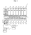
- FIG. 1 illustrates a structure of an information processing system according to an embodiment of the present invention.
- Information processing system 1 has one or more system boards and one or more IO units connected with the system boards through a system bus, system interconnection bus 4.
- Information processing system 1 shown in FIG. 1 has eight system boards, 2-1 through 2-8, and the eight IO units, 3-1 through 3-8.
- Each system board includes one or more equivalent CPUs and memory 22 that is shared by the CPUs.
- Each system board shown in FIG. 1 includes four CPUs, 21-1 through 21-4.
- Each CPU 21-n (n is an integral number greater than 1) controls a connection with each IO unit 3-1 through 3-8.
- Each CPU has a driver 23-n for configuring a setting value of data list word (DLW) stored in a channel operation buffer (COB) described in detail below.
- DLW data list word
- COB channel operation buffer
- Each of IO units 3-1 through 3-8 has a universal bus such as a peripheral component interconnect (PCI) bus that is an internal input-output device of the information processing system 1 and bridged with the system bus 4 internally.
- PCI peripheral component interconnect
- the PCI bus is not shown in the accompanying drawings.
- On the IO units 3-1 through 3-8 are mounted, for example, hard disk drives 31, channel devices 32, a LAN port and an input-output unit such as a CD-ROM drive or a DVD drive though a universal bus.
- IO unit 3-1 shown in FIG. 1 has four hard disk drives 31-1 through 31-4 and four channel devices 32-1 through 32-4.
- IO units 3-2 through 3-8 are not considered to be limited to the structure disclosed above. Each of IO units 3-2 through 3-8 may have only hard disk drive 31 or have the LAN port, or other different structure.
- Channel device 32 is a communication card device connecting information processing system 1 and an external IO device 5.
- the IO devices 5-1 through 5-n are external input-output devices such as hard disk drives, RAID, etc. and are connected with information processing system 1 through channel device 32.
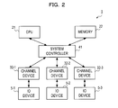
- FIG. 2 is a schematic view of information processing system 1 shown in FIG. 1 .
- Information processing system 1 includes a CPU 21, a memory 22, one or more channel devices that are connected with system controller 41 including system bus 4 and the bridge in IO unit 3 shown in FIG. 1 .
- Information processing system shown in FIG. 1 has three channel devices 32-1 through 32-3.
- Each of the channel devices 32-1 through 32-3 is connected with one of external IO devices 5-1 through 5-3 respectively.
- FIG. 2 illustrates the data transfer method of transferring data between memory 22 and IO device 5 through channel device 32 and the structure for implementing the data transfer method.
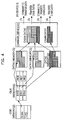
- FIG. 3 illustrates an example of a structure of channel device 32 according to an embodiment of the present invention.
- Channel device 32 shown in FIG. 3 has a PCI bus controller 51, a channel controller 52, a data transfer controller 53 and an IO controller 54.
- PCI bus controller 51 controls a connection with the PCI bus in IO unit 3, which is bridged with the system bus 4.
- Channel controller 52 controls the entire operation of the channel device 32.
- Data transfer controller 53 controls data exchange between the memory 22 incorporated in information processing system 1 and IO device 5.
- IO controller 54 controls a connection with the IO interface incorporated in the IO device 5.
- Data transfer controller 53 has a DLW controller 61, a transfer controller 62, a chain data controller 63, a memory transfer controller 64, a data buffer unit 65 and an IO transfer controller 66.
- DLW controller 131 controls reading of the DLW stored in memory 22 incorporated in information processing system 1 when processing the chain data.
- the DLW will be disclosed later.
- Transfer controller 62 controls the entire operation of the data transfer controller 53.
- Operation(s) of the chain data controller 63 controls the chain data processing in an embodiment of the present invention.
- Chain data controller 63 is disclosed below in detail.
- Memory transfer controller 64 receives the data stored in memory 22 through PCI bus controller 51 and writes the data to data buffer unit 65, or transfers the data stored in data buffer unit 65 to memory 22 through PCI bus controller 51.
- Data buffer unit 65 is a buffer memory compensating for a difference between the rates of transmissions from memory 22 and from the IO device 5.
- IO transfer controller 66 transfers the data stored in data buffer unit 65 to IO device 5 through IO controller 54, or writes the data sent from IO device 5 to data buffer unit 65.
- FIG. 4 illustrates transferring of data by the chain data processing according to an embodiment of the present invention.
- Driver 23 ( FIG. 1 ) allocates a COB (channel operation buffer) area in memory 22 before starting to transfer data by the chain data processing according to an embodiment of the present invention.
- the COB area is a buffer memory for storing operation commands issued by the driver 23 to the channel device 32.
- Driver 23 provides information for a starting channel device 32 in the COB area.
- Data list word address (DLWA) listed in an address list i.e., data list word (DLW)
- DLW data list word
- TNG total data transfer amount
- An address list of the DLW is provided in continuous areas in the memory, associating the data transfer start addresses (DTA 0, DTA 1 and DTA 2) of the data distributed to the multiple areas in memory 22 (data 0, data 1 and data 2) with the data length of each data (LNG 0, LNG 1 and LNG 2) and storing the addresses and the data lengths.
- the DLWA represents the first address of the DLW.
- the chain data processing is executed as follows.
- the driver 23 issues a command for accessing the IO device 5 to channel device 32.
- Channel device 32 reads the information from the COB area in memory 22 and executes the chain data processing in accordance with the information stored in the COB area.
- DLW controller 61 included in channel device 32 reads DLW in order according to the DLWA of the DLW read from the COB area. Then DLW controller 61 transfers the data between data buffer unit 65included in channel device 32 shown in FIG. 3 and memory 22according to data transfer start address, DTA n , and data length, LNG n. When the data transfer according to the one of the DLW are completed, DLW controller 61 reads the next DLW and transfers data between memory 22 and data buffer unit 65 continuously. DLW controller 61 repeats the process disclosed above until the data is transferred according to all the DLWs between memory 22 and data buffer unit 65.
- chain data controller 63 included in channel device 32 transfers data (chain data 0) between data buffer unit 65 and the IO device 5.
- a transmissible data size between data buffer unit 65 and the IO device 5 in the conventional transfer method shown in FIG. 9 is the same transmissible data size between the memory 22 and data buffer unit 65, i.e., 15K bytes.
- chain data 0 transferred from the buffer unit to the IO device is the same size as data 0.
- a total amount of data transferred by the chain data processing is represented by a total data length (TLNG).
- chain data controller 63 determines a data size transferred between the data buffer unit 65 included in the channel device 32 and the IO device 5 in accordance with a TLNG read from the COB area.
- the channel device 32 (1) issues a command for transferring the data to IO device to notify the data transfer amount determined by channel device 32; (2) transfers data (chain data 0) to the IO device 5 according to the data length; (3) commands to transfer the chain data to IO device if the data to be transferred remain in data buffer unit 65; (4) transfers the remaining data (chain data 1).
- the data is transferred between memory 22 and the IO device 5 effectively in fewer times.
- a data size of data 0 data 1 and data 2 transferred from memory 22 to data buffer unit 65 is the same transmissible data size in the conventional method shown in FIG. 9 , 15K bytes, respectively
- the data transfer between channel device 32 and the IO device 5 is completed with three transfers.
- a TLNG of chain data 0 determined by chain data controller 63 is 32K bytes according to the transfer method shown in FIG. 4 , the data transfer is complete with two transfers. Therefore, the data is transferred between memory 22 and the IO device 5 more effectively.
- a data transfer between the memory 22 and the IO device 5 at a time refers to operation(s) executed from when channel device 32 issues a command issued to the IO device 5 to when the data is transferred on the command.
- data 0, data 1 and data 2 are transferred by 15K bytes respectively and the chain data controller 63 determines the total transfer data amount at a time as 32K bytes according to the TLNG read from the COB area. Therefore, the data is transferred between channel device 32 and the IO device 5 with two transfers.
- data may be transferred in the same amount of chain data 0, i.e., 64K bytes, by combining the chain data command and the data distributed to the multiple areas in the memory after executing the process (2) shown in FIG. 4 .
- the chain data transfer between the memory and the channel device or between the channel device and the IO device is controlled independently.
- the transmissible data size between the memory and the channel device at a time is different from the data transfer unit between the channel device and the IO device at a time. Therefore, the data is transferred effectively between the memory and the IO device.
- FIG. 5 shows clarifying (identifying) a breakpoint of the chain data transferred to the IO device 5 last and transferring the chain data.
- FIG. 5 shows that operation(s) of a write command, i.e., the data transfer from the memory to the IO device 5.
- Operations on a read command i.e., the data transfer from the IO device to the memory, is basically the same as the operations on the write command shown in FIG. 5 except a data is transferred in a reverse direction.
- a last byte count (LBC) of the data to be transferred is configured in the COB shown in FIG. 5 in addition to the DLWA of the DLW and the TLNG shown in FIG. 4 .
- the LBC indicates a data length of chain data 2 that are transferred from memory 22 last, LNG 2.
- the chain data controller 63 included in the channel device 32 (1) determines a total data length (TLNG) of data transferred from channel device 32 to the IO device 5 according to the LBC and notifies the TLNG to the IO device; (2) the data is transferred to the IO device 5; (3 and 4) remaining data specified by the LBC are transferred. Therefore, the breakpoint of the chain data is clarified and transferred to the IO device 5.
- TLNG total data length
- FIG. 6 shows the case that data to be transferred to the IO device 5 excluding the chain data (the data is shown clearly in FIG. 6 ) are not transferred at a time.
- the data excluding the chain data that are transferred to the IO device 5 lastly are transferred in an order by the data length determined based on a difference between the TLNG and the LBC, e.g., 32K bytes (1, 2) and then the remaining data (chain data 1) are transferred (3, 4).
- chain data 2 to be transferred to the IO device 5 last are transferred.
- the chain data is transferred by clarifying (identifying) a breakpoint of last chain data transferred to the IO device .
- chain data controller 63 included in the channel device 32 will be discloses.
- FIG. 7 is the block diagram illustrating a structure of a data transfer controller.
- Transfer controller 62 shown in FIG. 7 has three registers: buffer byte count (BBC) register 71, command (CMD) register 72 and IO data length (IDL) register.
- BBC buffer byte count
- CMD command
- IDL IO data length
- BBC register 71 represents a byte count of valid data stored in data buffer unit 65 in transferring data. A value of BBC register 71 is reset on starting the data transfer. The value of BBC register 71 is notified to chain data controller 63.
- CMD register 72 is used for storing coded values of commands issued to the IO device 5. The coded command stored in CMD register 72 is notified to chain data controller 63 as a WRITE (WT) command.
- WT command is a value representing a transfer direction of data decoded the value stored in CMD register 72. When data is transferred from memory 22 to the IO device 5, the value is "1". When data is transferred from the IO device 5 to memory 22, the value is "0".
- Chain data controller 63 has last byte count (LBC) register 74, comparator 75 (a first comparison), IBC register 76 and comparator 77 (a second comparator).
- LBC last byte count
- LBC register 74 is used for configuring a byte count relating to the last chain data, which is notified to the IO device 5 from channel device 32.
- the value of the LBC configured in the COB is configured in LBC register 74 before a first command is output to the IO device 5.
- IBC (IO byte count) register 76 represents a byte count of the remaining data to be transferred between channel device 32 and the IO device 5.
- IBC register 76 decreases the byte count when the data is transferred between channel device 32 and the IO device 5.
- IBC register 76 is used for detecting and end of the chain data transfer between the channel device and the IO device. The value stored in IBC register 76 is notified to IO transfer controller 66.
- the comparator 75 compares a value stored in IDL register 73 and a value stored in LBC register 74 upon a transmission command frame at first (TCMFT) signal is on when a first command is output to the IO device on a command for transferring the data issued by IO transfer controller 66. Based upon a comparison result, comparator 75 configures a value in IBC register 76. The TCMFT signal becomes valid when the first command is output to the IO device 5 on the command for transferring the data. Additionally, comparator 75 (the first comparison) outputs a chain data flag (CDF) signal that becomes valid when a command issued to be transferred to the IO device 5, whose chain data flag is on, is issued to IO transfer controller 66. A size or the length of data to be transferred from data buffer unit 65 included in the channel device 32 to the IO device 5 at a time is determined by setting the value in IBC register 76 by comparator 74 (the first comparison).
- TCMFT transmission command frame at first
- Comparator 77 (the second comparison) checks a value stored in BBC register 71 and a WT command obtained by decoding the coded command stored in CMD register 72 where when the value stored in IBC register 76 becomes "0", i.e., the data transfer from the data buffer unit 65 to the IO device 5 completes.
- the value stored in BBC register 71 becomes "0", i.e., there are no valid data in data buffer unit 65, or the value of the WT command is 1 ", i.e., a command issued to the IO device is a write command
- comparator 77 (the second comparison) outputs a transmission command frame at chain data (TCMCD) signal to IO transfer controller 66.
- TCMCD transmission command frame at chain data
- FIG. 8 is the flow chart illustrating operation(s) executed by a channel device in transferring data.
- initial value(s) are set, for example, in BBC register 71, CMD register 72, IDL register 73 and LBC register 74 for the data transfer in operation S1.
- the value of the TLNG read from the COB is configured in the IDL register included in transfer controller 62.
- the value coded the command issued to the IO device is configured in CMD register 72.
- the value stored in BBC register 71 is reset to "0".
- the byte count relating to the last chain data is configured in LBC register 74 included in chain data controller 63.
- channel device 32 commands the IO device 5 to transfer data.
- IO transfer controller 66 sets the TCMFT signal to chain data controller 63 to "1" when the first command can be output to the IO interface.
- chain data controller 63 starts to determine a transmissible data size between the channel device and the IO device.
- chain data controller 63 included in channel device 32 compares the value stored in IDL register 73 with the value stored in LBC register 74 in operation S3. If the value stored in IDL register 73 is greater than the value stored in LBC register (operation S3, No), chain data controller 63 judges whether a value derived by subtracting the value stored in LBC register 74 from the value stored in IDL register 73 is greater than 64K bytes. When the value is greater than 64K bytes (operation S4, Yes), the value stored in IBC register 76 is set to 32K bytes and the CDF signal is set to "1" in operation S6. Then the process moves on to operation S8. For example, a maximum transmissible data size is 64K bytes in an embodiment.
- the remaining data is transferred in a size of 32K bytes.
- the value of the transmissible data size is not considered to be limited to 32K bytes. Any value(s) equal to or less than 64K bytes may be processed accordingly.
- the value stored in IBC register 76 is configured to the derived by subtracting the value stored in the LBC register 74 from the value stored in IDL register 73 and the CDF signal is configured to "1" in operation S5. Then the process moves on to operation S8.
- the value stored in IDL register 73 is equal to or less than the value stored in LBC register 74 in operation S3 (Yes), the value stored in IBC register 76 is configured to the value stored in IDL register 73 and the CDF signal is configured to "0" in operation S7 and complete the process.
- the transmissible data size between channel device 32 and the IO device 5 at a time is determined by setting value(s) stored in IBC register 76 in the processes in operations S3 through S7 and the value of the chain data flag is determined according to the CDF signal.
- the data transfer between the channel device 32 and the IO device 5 starts and the value stored in the IBC register is decreased according to the transmissible data size.
- IBC register 76 represents the byte count of the remaining data to be transferred between the channel device 32 and the IO device 5.
- chain data controller 63 checks the WR value obtained from CMD register 72 to confirm whether the output command is a read command or a write command in operation S9.
- the command is the read command (operation S9, No)
- chain data controller 63 checks whether data buffer unit 65 has sufficient available space and waits until the sufficient space is freed (operation S10, No). If there is the available space in the data buffer unit, the process moves on to operation S11.
- chain data controller 63 configures the TCMCD signal to IO transfer controller 66 to "1", i.e., configures the TCMDC "on”. Then the process goes back to operation S3, and a size of data to be transferred between the channel device 32 and the IO device 5 and a value of the CDF signal are determined on the updated command. Operations S3 through S10 are repeated until all the data are transferred and the value of the CDF signal is configured to "0".
- the data are divided by 32K bytes and transferred to the IO device 5 by channel device 32 in the chain data processing shown in FIG. 8 .
- the transmissible data size of the remaining data derived by subtracting the LBC from the IDL becomes less than 64K bytes
- the data less than 64K bytes are transferred to the IO device 5 in a lump.
- the LBC of the chain data are transferred last.
- the data distributed to the multiple areas in the memory are transferred to the IO device in a specific data length configured by channel device 32. Therefore, the latency time for the IO interface is decreased and the transmission performance is improved.
Landscapes
- Engineering & Computer Science (AREA)
- Theoretical Computer Science (AREA)
- Health & Medical Sciences (AREA)
- Heart & Thoracic Surgery (AREA)
- Life Sciences & Earth Sciences (AREA)
- General Engineering & Computer Science (AREA)
- Veterinary Medicine (AREA)
- Biomedical Technology (AREA)
- Physics & Mathematics (AREA)
- Public Health (AREA)
- General Physics & Mathematics (AREA)
- Animal Behavior & Ethology (AREA)
- General Health & Medical Sciences (AREA)
- Hematology (AREA)
- Anesthesiology (AREA)
- Vascular Medicine (AREA)
- Bus Control (AREA)
- Computer And Data Communications (AREA)
- Information Transfer Systems (AREA)
Applications Claiming Priority (1)
| Application Number | Priority Date | Filing Date | Title |
|---|---|---|---|
| JP2008046110A JP5226341B2 (ja) | 2008-02-27 | 2008-02-27 | チャネル装置、情報処理システム、及びデータ転送方法 |
Publications (1)
| Publication Number | Publication Date |
|---|---|
| EP2096551A1 true EP2096551A1 (en) | 2009-09-02 |
Family
ID=40548974
Family Applications (1)
| Application Number | Title | Priority Date | Filing Date |
|---|---|---|---|
| EP09153459A Ceased EP2096551A1 (en) | 2008-02-27 | 2009-02-23 | Channel device, information processing system and data transfer method |
Country Status (5)
| Country | Link |
|---|---|
| US (1) | US8769167B2 (zh) |
| EP (1) | EP2096551A1 (zh) |
| JP (1) | JP5226341B2 (zh) |
| KR (1) | KR101068541B1 (zh) |
| CN (1) | CN101520760B (zh) |
Cited By (2)
| Publication number | Priority date | Publication date | Assignee | Title |
|---|---|---|---|---|
| WO2016093990A1 (en) * | 2014-12-10 | 2016-06-16 | Qualcomm Incorporated | Processing unaligned block transfer operations |
| FR3047577A1 (fr) * | 2016-02-10 | 2017-08-11 | Upmem | Instruction combinee d'addition et de verification de bornes |
Families Citing this family (1)
| Publication number | Priority date | Publication date | Assignee | Title |
|---|---|---|---|---|
| US8549182B2 (en) * | 2010-06-23 | 2013-10-01 | International Business Machines Corporation | Store/store block instructions for communicating with adapters |
Citations (4)
| Publication number | Priority date | Publication date | Assignee | Title |
|---|---|---|---|---|
| US5708849A (en) * | 1994-01-26 | 1998-01-13 | Intel Corporation | Implementing scatter/gather operations in a direct memory access device on a personal computer |
| WO1999034273A2 (en) * | 1997-12-30 | 1999-07-08 | Lsi Logic Corporation | Automated dual scatter/gather list dma |
| WO2004104846A2 (en) * | 2003-05-26 | 2004-12-02 | Koninklijke Philips Electronics N.V. | Method and device for transferring data between a main memory and a storage device |
| JP2008046110A (ja) | 2006-07-20 | 2008-02-28 | Canon Inc | 液滴の形状計測方法及び装置 |
Family Cites Families (18)
| Publication number | Priority date | Publication date | Assignee | Title |
|---|---|---|---|---|
| JPS5911135B2 (ja) | 1979-01-17 | 1984-03-13 | 株式会社日立製作所 | デ−タ処理システムのデ−タ転送方式 |
| JPS59177634A (ja) * | 1983-03-29 | 1984-10-08 | Fujitsu Ltd | 入力バツフアの全入力デ−タ長計数方式 |
| JPS61151765A (ja) * | 1984-12-26 | 1986-07-10 | Toshiba Corp | 入出力処理方式 |
| JPH01281553A (ja) | 1988-05-07 | 1989-11-13 | Fujitsu Ltd | チャンネル制御方式 |
| JPH0690900B2 (ja) * | 1988-11-14 | 1994-11-14 | 株式会社キーエンス | 多光軸光電スイッチ |
| US5809527A (en) * | 1993-12-23 | 1998-09-15 | Unisys Corporation | Outboard file cache system |
| US5860022A (en) * | 1994-07-26 | 1999-01-12 | Hitachi, Ltd. | Computer system and method of issuing input/output commands therefrom |
| JP3588705B2 (ja) * | 1995-06-12 | 2004-11-17 | 株式会社キーエンス | 検出スイッチ親機、検出スイッチ子機および検出スイッチシステム |
| US5802546A (en) * | 1995-12-13 | 1998-09-01 | International Business Machines Corp. | Status handling for transfer of data blocks between a local side and a host side |
| JP3223420B2 (ja) * | 1996-03-18 | 2001-10-29 | 株式会社キーエンス | 検出スイッチ |
| JP3484056B2 (ja) | 1996-10-18 | 2004-01-06 | 松下電器産業株式会社 | データ転送装置及びデータ転送システム |
| US6018746A (en) * | 1997-12-23 | 2000-01-25 | Unisys Corporation | System and method for managing recovery information in a transaction processing system |
| JP2000298641A (ja) * | 1999-04-15 | 2000-10-24 | Nec Corp | 情報処理装置およびそのデータ転送方法ならびにデータ転送制御プログラムを格納した記憶媒体 |
| US6560677B1 (en) * | 1999-05-04 | 2003-05-06 | International Business Machines Corporation | Methods, cache memories, systems and computer program products for storing transient, normal, and locked entries in an associative cache memory |
| CN1282925A (zh) * | 1999-07-12 | 2001-02-07 | 松下电器产业株式会社 | 数据处理装置 |
| US7006942B2 (en) * | 2001-09-27 | 2006-02-28 | Keyence Corporation | Sensor management system and computer-readable medium for sensor management program |
| JP4212970B2 (ja) * | 2003-06-30 | 2009-01-21 | 株式会社キーエンス | 安全リレーシステム |
| JP2006259898A (ja) * | 2005-03-15 | 2006-09-28 | Toshiba Corp | I/oコントローラ、信号処理システム、およびデータ転送方法 |
-
2008
- 2008-02-27 JP JP2008046110A patent/JP5226341B2/ja active Active
-
2009
- 2009-02-11 US US12/369,445 patent/US8769167B2/en active Active
- 2009-02-23 EP EP09153459A patent/EP2096551A1/en not_active Ceased
- 2009-02-26 KR KR1020090016327A patent/KR101068541B1/ko active IP Right Grant
- 2009-02-26 CN CN2009101185409A patent/CN101520760B/zh active Active
Patent Citations (4)
| Publication number | Priority date | Publication date | Assignee | Title |
|---|---|---|---|---|
| US5708849A (en) * | 1994-01-26 | 1998-01-13 | Intel Corporation | Implementing scatter/gather operations in a direct memory access device on a personal computer |
| WO1999034273A2 (en) * | 1997-12-30 | 1999-07-08 | Lsi Logic Corporation | Automated dual scatter/gather list dma |
| WO2004104846A2 (en) * | 2003-05-26 | 2004-12-02 | Koninklijke Philips Electronics N.V. | Method and device for transferring data between a main memory and a storage device |
| JP2008046110A (ja) | 2006-07-20 | 2008-02-28 | Canon Inc | 液滴の形状計測方法及び装置 |
Cited By (6)
| Publication number | Priority date | Publication date | Assignee | Title |
|---|---|---|---|---|
| WO2016093990A1 (en) * | 2014-12-10 | 2016-06-16 | Qualcomm Incorporated | Processing unaligned block transfer operations |
| CN107003964A (zh) * | 2014-12-10 | 2017-08-01 | 高通股份有限公司 | 处理未对准块传送操作 |
| US9818170B2 (en) | 2014-12-10 | 2017-11-14 | Qualcomm Incorporated | Processing unaligned block transfer operations |
| FR3047577A1 (fr) * | 2016-02-10 | 2017-08-11 | Upmem | Instruction combinee d'addition et de verification de bornes |
| WO2017137675A1 (fr) * | 2016-02-10 | 2017-08-17 | Upmem | Instruction combinée d'addition et de vérification de bornes |
| US10817288B2 (en) | 2016-02-10 | 2020-10-27 | Upmem | Combined instruction for addition and checking of terminals |
Also Published As
| Publication number | Publication date |
|---|---|
| CN101520760A (zh) | 2009-09-02 |
| KR20090092722A (ko) | 2009-09-01 |
| US8769167B2 (en) | 2014-07-01 |
| CN101520760B (zh) | 2013-01-23 |
| JP5226341B2 (ja) | 2013-07-03 |
| KR101068541B1 (ko) | 2011-09-30 |
| JP2009205366A (ja) | 2009-09-10 |
| US20090216919A1 (en) | 2009-08-27 |
Similar Documents
| Publication | Publication Date | Title |
|---|---|---|
| US6049842A (en) | Efficient data transfer mechanism for input/output devices | |
| US8352663B2 (en) | Data storage apparatus and method of data transfer | |
| US6647438B1 (en) | Direct memory access transfer reduction method and apparatus to overlay data on to scatter gather descriptors for bus-mastering I/O controllers | |
| EP2097828B1 (en) | Dmac to handle transfers of unknown lengths | |
| US20030056032A1 (en) | Method and apparatus for automatically transferring i/o blocks between a host system and a host adapter | |
| US6697906B1 (en) | Semiconductor device supporting integrated data transfer bridging between CPU memory and I/O device | |
| US7865653B2 (en) | Universal serial bus host controller and control methods thereof | |
| JPS6375955A (ja) | プログラムモ−ド・アクセス制御方式 | |
| EP0772831B1 (en) | Bidirectional parallel signal interface | |
| EP2096551A1 (en) | Channel device, information processing system and data transfer method | |
| US20060095637A1 (en) | Bus control device, arbitration device, integrated circuit device, bus control method, and arbitration method | |
| US6751686B2 (en) | Automated transfer of a data unit comprising a plurality of fundamental data units between a host device and a storage medium | |
| CN101599049B (zh) | 控制dma访问不连续物理地址的方法及dma控制器 | |
| US6584512B1 (en) | Communication DMA device for freeing the data bus from the CPU and outputting divided data | |
| US7185122B2 (en) | Device and method for controlling data transfer | |
| KR100638378B1 (ko) | 디스크 제어장치의 메모리 구조에 대한 시스템 및 방법 | |
| US6772311B2 (en) | ATAPI device unaligned and aligned parallel I/O data transfer controller | |
| KR101485081B1 (ko) | 간접 액세스가능 메모리를 구비한 컨트롤러 | |
| US7287102B1 (en) | System and method for concatenating data | |
| US9110856B2 (en) | Interface control apparatus, data storage apparatus and method for interface control | |
| US7921238B2 (en) | USB host system and method for transferring transfer data | |
| US20080104286A1 (en) | Data transfer apparatus and data transfer method | |
| JP2003085125A (ja) | メモリ制御器及びメモリ制御方法 | |
| KR20050004157A (ko) | 다중 코히런시 단위들을 지원하는 데이터 전송 유닛 | |
| JP2533886B2 (ja) | デ―タ転送方式 |
Legal Events
| Date | Code | Title | Description |
|---|---|---|---|
| PUAI | Public reference made under article 153(3) epc to a published international application that has entered the european phase |
Free format text: ORIGINAL CODE: 0009012 |
|
| AK | Designated contracting states |
Kind code of ref document: A1 Designated state(s): AT BE BG CH CY CZ DE DK EE ES FI FR GB GR HR HU IE IS IT LI LT LU LV MC MK MT NL NO PL PT RO SE SI SK TR |
|
| AX | Request for extension of the european patent |
Extension state: AL BA RS |
|
| 17P | Request for examination filed |
Effective date: 20100301 |
|
| AKX | Designation fees paid |
Designated state(s): DE FR GB |
|
| 17Q | First examination report despatched |
Effective date: 20100609 |
|
| STAA | Information on the status of an ep patent application or granted ep patent |
Free format text: STATUS: THE APPLICATION HAS BEEN REFUSED |
|
| 18R | Application refused |
Effective date: 20131002 |