EP2096423A2 - Dispositif de détection - Google Patents
Dispositif de détection Download PDFInfo
- Publication number
- EP2096423A2 EP2096423A2 EP08105868A EP08105868A EP2096423A2 EP 2096423 A2 EP2096423 A2 EP 2096423A2 EP 08105868 A EP08105868 A EP 08105868A EP 08105868 A EP08105868 A EP 08105868A EP 2096423 A2 EP2096423 A2 EP 2096423A2
- Authority
- EP
- European Patent Office
- Prior art keywords
- sensor element
- carrier
- housing
- sensor
- region
- Prior art date
- Legal status (The legal status is an assumption and is not a legal conclusion. Google has not performed a legal analysis and makes no representation as to the accuracy of the status listed.)
- Withdrawn
Links
Images
Classifications
-
- G—PHYSICS
- G01—MEASURING; TESTING
- G01L—MEASURING FORCE, STRESS, TORQUE, WORK, MECHANICAL POWER, MECHANICAL EFFICIENCY, OR FLUID PRESSURE
- G01L19/00—Details of, or accessories for, apparatus for measuring steady or quasi-steady pressure of a fluent medium insofar as such details or accessories are not special to particular types of pressure gauges
- G01L19/14—Housings
- G01L19/141—Monolithic housings, e.g. molded or one-piece housings
-
- G—PHYSICS
- G01—MEASURING; TESTING
- G01L—MEASURING FORCE, STRESS, TORQUE, WORK, MECHANICAL POWER, MECHANICAL EFFICIENCY, OR FLUID PRESSURE
- G01L19/00—Details of, or accessories for, apparatus for measuring steady or quasi-steady pressure of a fluent medium insofar as such details or accessories are not special to particular types of pressure gauges
- G01L19/14—Housings
- G01L19/148—Details about the circuit board integration, e.g. integrated with the diaphragm surface or encapsulation
-
- H—ELECTRICITY
- H01—ELECTRIC ELEMENTS
- H01L—SEMICONDUCTOR DEVICES NOT COVERED BY CLASS H10
- H01L2224/00—Indexing scheme for arrangements for connecting or disconnecting semiconductor or solid-state bodies and methods related thereto as covered by H01L24/00
- H01L2224/01—Means for bonding being attached to, or being formed on, the surface to be connected, e.g. chip-to-package, die-attach, "first-level" interconnects; Manufacturing methods related thereto
- H01L2224/42—Wire connectors; Manufacturing methods related thereto
- H01L2224/47—Structure, shape, material or disposition of the wire connectors after the connecting process
- H01L2224/48—Structure, shape, material or disposition of the wire connectors after the connecting process of an individual wire connector
- H01L2224/481—Disposition
- H01L2224/48135—Connecting between different semiconductor or solid-state bodies, i.e. chip-to-chip
- H01L2224/48137—Connecting between different semiconductor or solid-state bodies, i.e. chip-to-chip the bodies being arranged next to each other, e.g. on a common substrate
-
- H—ELECTRICITY
- H01—ELECTRIC ELEMENTS
- H01L—SEMICONDUCTOR DEVICES NOT COVERED BY CLASS H10
- H01L2224/00—Indexing scheme for arrangements for connecting or disconnecting semiconductor or solid-state bodies and methods related thereto as covered by H01L24/00
- H01L2224/01—Means for bonding being attached to, or being formed on, the surface to be connected, e.g. chip-to-package, die-attach, "first-level" interconnects; Manufacturing methods related thereto
- H01L2224/42—Wire connectors; Manufacturing methods related thereto
- H01L2224/47—Structure, shape, material or disposition of the wire connectors after the connecting process
- H01L2224/48—Structure, shape, material or disposition of the wire connectors after the connecting process of an individual wire connector
- H01L2224/484—Connecting portions
- H01L2224/4847—Connecting portions the connecting portion on the bonding area of the semiconductor or solid-state body being a wedge bond
- H01L2224/48472—Connecting portions the connecting portion on the bonding area of the semiconductor or solid-state body being a wedge bond the other connecting portion not on the bonding area also being a wedge bond, i.e. wedge-to-wedge
-
- H—ELECTRICITY
- H01—ELECTRIC ELEMENTS
- H01L—SEMICONDUCTOR DEVICES NOT COVERED BY CLASS H10
- H01L2224/00—Indexing scheme for arrangements for connecting or disconnecting semiconductor or solid-state bodies and methods related thereto as covered by H01L24/00
- H01L2224/73—Means for bonding being of different types provided for in two or more of groups H01L2224/10, H01L2224/18, H01L2224/26, H01L2224/34, H01L2224/42, H01L2224/50, H01L2224/63, H01L2224/71
- H01L2224/732—Location after the connecting process
- H01L2224/73251—Location after the connecting process on different surfaces
- H01L2224/73265—Layer and wire connectors
-
- H—ELECTRICITY
- H01—ELECTRIC ELEMENTS
- H01L—SEMICONDUCTOR DEVICES NOT COVERED BY CLASS H10
- H01L2924/00—Indexing scheme for arrangements or methods for connecting or disconnecting semiconductor or solid-state bodies as covered by H01L24/00
- H01L2924/15—Details of package parts other than the semiconductor or other solid state devices to be connected
- H01L2924/181—Encapsulation
- H01L2924/1815—Shape
Definitions
- the invention relates to a sensor arrangement with at least one sensor element which is arranged on a carrier, and with a mold housing, in which a region of the sensor element and the carrier is embedded, wherein the mold housing has at least one passage opening as an access opening for the sensitive region of the sensor element.
- the invention particularly relates to sensors, e.g. Pressure or air mass sensors or optical sensors that require application-related contact to a measuring medium.
- sensors e.g. Pressure or air mass sensors or optical sensors that require application-related contact to a measuring medium.
- the coupling of the sensor element to the environment therefore takes place via a sealed to the interior of the motor vehicle outer housing compound.
- the parts of the sensor to be protected are arranged on the inside, while the actual sensor component is exposed to environmental influences.
- the from the DE 10 205 038 443 A1 known sensor arrangement does not constitute a barrier to the measuring medium.
- the measuring medium enters the free space on one side of the housing, flows around the sensitive area of the sensor element and can then exit unhindered on the other side of the housing. For this reason, this sensor arrangement is not suitable for installation in a sealed connection between areas of space, such as in the interior of a motor vehicle outer casing.
- the passage opening in the housing housing can be closed easily and reliably with the aid of the carrier, by the carrier being correspondingly dimensioned and embedded in the edge region of the passage opening in the molding compound of the housing.
- the sensor element is integrated on one side only in the mold housing, so that the sensitive area protrudes into the passage opening of the mold housing. As already mentioned, this makes it possible to achieve a particularly good thermal decoupling of the sensitive area from the housing.
- the sensor element mounted on the support is overmolded with the molding compound of the housing, wherein a cutout is produced in the vicinity of the sensitive area.
- a cutout is produced in the vicinity of the sensitive area.
- connection between the sensor element and the carrier may be an adhesive connection. Due to the adhesive layer between the sensor element and the carrier in the region of the housing, the sensitive region is advantageously kept at a distance from the carrier. At least this can easily be ensured that the sensitive area of the sensor element rests loosely on the support.
- the carrier can also be thinned in at least one side in the region of the passage opening, so that the sensitive region of the sensor element is spaced from the carrier. This measure also contributes to the thermal decoupling of the sensitive area of the sensor element from the carrier.
- the sensor arrangement according to the invention can also be designed for applications in which the sensory area of the sensor element comes into contact with measuring media on both sides, such as, for example, B. in the differential pressure detection.
- the sensory area of the sensor element comprises at least one membrane, which can be seen from both the top and the bottom Also accessible from the back of the sensor element.
- the back pressure of this membrane via a trained in the carrier access opening below the membrane.
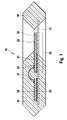
- a sensor element 20 which is arranged on a carrier 25.
- a micromechanical sensor structure 23 in the form of a membrane is formed over a closed volume.
- These Sensor structure 23 is used here for absolute pressure detection by detecting deformations of the diaphragm piezoresistively.
- the electrical connections of the piezoresistors required for this purpose are conducted into the region 21 of the sensor element 20, where parts of an evaluation circuit are also located. These circuit parts are connected via bonding wires 27 with an evaluation chip 26, which is also arranged on the carrier 25.
- the sensor arrangement 10 comprises a mold housing 30 with a cutout 31 as an access opening for the sensitive area 22 of the sensor element 20.
- the evaluation chip 26, the bonding wires 27 and the area 21 of the sensor element 20 are together with the corresponding portion of the carrier 25 in the molding compound embedded in the housing 30, so that the housing 30 protects these parts of the sensor assembly 10 not only against mechanical effects, but also against the measuring medium.
- the cutout 31 extends over the entire thickness of the mold housing 30 and thus forms a passage opening 31 in the housing 30.
- the support 25 extends over the entire cross section of the passage opening 31 and is embedded in the mold housing 30 in the edge region of the passage opening 31.
- the carrier 25 closes off the passage opening 31 and thus ensures a spatial separation between the housing top side and the housing bottom side of the sensor arrangement 10.
- the sensitive region 22 of the sensor element 20 protrudes freely into the through-opening 31 of the housing 30. As a result, the sensitive region 22 from the housing 30 is substantially thermal decoupled.
- only the embedded in the mold housing 30 region 21 of the sensor element 20 is connected via an adhesive layer 28 to the carrier 25.
- the sensitive region 22 of the sensor element 20 is loosely on the carrier 25 or even spaced therefrom.
- the sensitive region 22 of the sensor element 20 is also largely thermally decoupled from the carrier 25, so that different temperature coefficients of the carrier material and of the sensor element 20 do not lead to thermally induced mechanical stresses in the sensitive region 22 of the sensor element 20.
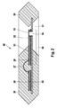
- sensor assembly 40 corresponds substantially to the structure of the sensor assembly 10, so that the same components are provided with the same reference numerals.
- the sensor arrangement 40 comprises a sensor element 50 which is arranged on a carrier 55.
- the sensor arrangement 40 is used for differential pressure detection. Accordingly, the membrane 53 formed in the sensor region 52 of the sensor element 50 can be subjected to pressure both from the top side and from the rear side, which will be explained in more detail below.
- the membrane deformations are also piezoresistively detected and evaluated using a chip 26.
- the electrical connections of the piezoresistors are led into the region 51 of the sensor element 50 and connected via bonding wires 27 to an evaluation chip 26, which is likewise arranged on the carrier 55.
- the evaluation chip 26, the bonding wires 27 and the region 51 of the sensor element 50 are embedded together with the corresponding portion of the carrier 55 in a mold housing 30, so that the housing 30 protects these parts of the sensor assembly 40 not only against mechanical effects, but also against the Measuring medium.
- a cutout 31 is formed as an access opening for the sensitive area 52 of the sensor element 50.
- the carrier 55 extends over the entire cross section of this passage opening 31 and is embedded in the edge region in the mold housing 30.
- the sensor element 50 While the entire edge region of the carrier 55 is embedded in the molding compound of the housing 30, the sensor element 50 is integrated into the housing 30 on only one side, so that the sensitive region 52 projects into the through-opening 31 of the housing 30. As a result, a very good thermal decoupling of the sensitive region 52 from the housing 30 is achieved. In addition, the clamping forces acting on the sensor element 50 are very well degraded by the lateral removal of the membrane 53 to the molding compound of the housing 30.
- the differential pressure sensing diaphragm 53 is pressurized both from the top of the sensor element 50 and from the rear side thereof.
- the back pressure is applied via a correspondingly arranged access opening 56 in the support 55 in the region of the passage opening 31 in the mold housing 30.
- the region 51 arranged in the mold housing 30 is here of the sensor element 50 is connected to the carrier 55, but also the sensitive region 52, which projects into the passage opening 31 of the housing 30.
- This pressure-tight connection is realized here by means of an adhesive layer 28.
Landscapes
- Physics & Mathematics (AREA)
- General Physics & Mathematics (AREA)
- Measuring Fluid Pressure (AREA)
Applications Claiming Priority (1)
| Application Number | Priority Date | Filing Date | Title |
|---|---|---|---|
| DE102008011943A DE102008011943B4 (de) | 2008-02-29 | 2008-02-29 | Sensoranordnung zur Differenzdruckmessung |
Publications (2)
| Publication Number | Publication Date |
|---|---|
| EP2096423A2 true EP2096423A2 (fr) | 2009-09-02 |
| EP2096423A3 EP2096423A3 (fr) | 2013-10-16 |
Family
ID=40451393
Family Applications (1)
| Application Number | Title | Priority Date | Filing Date |
|---|---|---|---|
| EP08105868.7A Withdrawn EP2096423A3 (fr) | 2008-02-29 | 2008-11-26 | Dispositif de détection |
Country Status (2)
| Country | Link |
|---|---|
| EP (1) | EP2096423A3 (fr) |
| DE (1) | DE102008011943B4 (fr) |
Cited By (6)
| Publication number | Priority date | Publication date | Assignee | Title |
|---|---|---|---|---|
| EP2339302A3 (fr) * | 2009-12-11 | 2011-07-06 | Hitachi Automotive Systems, Ltd. | Débitmètre, procédé de fabrication du débitmètre et module de débitmètre |
| JP2013098480A (ja) * | 2011-11-04 | 2013-05-20 | Denso Corp | 半導体パッケージおよびその製造方法。 |
| JP2014185865A (ja) * | 2013-03-21 | 2014-10-02 | Hitachi Automotive Systems Ltd | 熱式流量計 |
| EP2629065A4 (fr) * | 2010-10-13 | 2017-12-13 | Hitachi Automotive Systems, Ltd. | Capteur d'écoulement et procédé de production pour celui-ci, et module de capteur d'écoulement et procédé de production pour celui-ci |
| EP3683031A1 (fr) * | 2019-01-21 | 2020-07-22 | Melexis Technologies NV | Procédé de fabrication d'un dispositif de capteur et structure de support de moulage |
| EP3617686B1 (fr) * | 2018-08-31 | 2021-10-27 | Melexis Technologies NV | Capteur de pression et procédé de détection de pression |
Families Citing this family (6)
| Publication number | Priority date | Publication date | Assignee | Title |
|---|---|---|---|---|
| DE102008043517B4 (de) | 2008-11-06 | 2022-03-03 | Robert Bosch Gmbh | Sensormodul und Verfahren zur Herstellung eines Sensormoduls |
| DE102009002584A1 (de) | 2009-04-23 | 2010-10-28 | Robert Bosch Gmbh | Sensoranordnung |
| DE102010001073A1 (de) | 2010-01-21 | 2011-07-28 | Robert Bosch GmbH, 70469 | Sensor, insbesondere Niederdrucksensor, zur Messung eines Differenzdrucks |
| DE102010043982A1 (de) | 2010-11-16 | 2011-12-15 | Robert Bosch Gmbh | Sensoranordnung |
| DE102012215235A1 (de) | 2012-08-28 | 2013-05-23 | Robert Bosch Gmbh | Sensorbauteil |
| DE102014006037A1 (de) | 2013-04-29 | 2014-10-30 | Elmos Semiconductor Ag | MEMS Sensor für schwierige Umgebungen und Medien |
Citations (1)
| Publication number | Priority date | Publication date | Assignee | Title |
|---|---|---|---|---|
| DE102005038443A1 (de) | 2005-08-16 | 2007-02-22 | Robert Bosch Gmbh | Sensoranordnung mit einem Substrat und mit einem Gehäuse und Verfahren zur Herstellung einer Sensoranordnung |
Family Cites Families (6)
| Publication number | Priority date | Publication date | Assignee | Title |
|---|---|---|---|---|
| JP3545637B2 (ja) * | 1999-03-24 | 2004-07-21 | 三菱電機株式会社 | 感熱式流量センサ |
| DE19929025A1 (de) * | 1999-06-25 | 2000-12-28 | Bosch Gmbh Robert | Drucksensor |
| DE50212957D1 (de) * | 2002-04-12 | 2008-12-11 | Grundfos As | Drucksensor |
| DE102004003413A1 (de) * | 2004-01-23 | 2005-08-11 | Robert Bosch Gmbh | Verfahren zum Verpacken von Halbleiterchips und entsprechende Halbleiterchipanordnung |
| DE102004035893B4 (de) * | 2004-07-23 | 2013-03-14 | Robert Bosch Gmbh | Vorrichtung zur Bestimmung wenigstens eines Parameters eines in einer Leitung strömenden Mediums |
| DE102004051468A1 (de) * | 2004-10-22 | 2006-04-27 | Robert Bosch Gmbh | Verfahren zum Montieren von Halbleiterchips und entsprechende Halbleiterchipanordnung |
-
2008
- 2008-02-29 DE DE102008011943A patent/DE102008011943B4/de not_active Expired - Fee Related
- 2008-11-26 EP EP08105868.7A patent/EP2096423A3/fr not_active Withdrawn
Patent Citations (1)
| Publication number | Priority date | Publication date | Assignee | Title |
|---|---|---|---|---|
| DE102005038443A1 (de) | 2005-08-16 | 2007-02-22 | Robert Bosch Gmbh | Sensoranordnung mit einem Substrat und mit einem Gehäuse und Verfahren zur Herstellung einer Sensoranordnung |
Cited By (13)
| Publication number | Priority date | Publication date | Assignee | Title |
|---|---|---|---|---|
| US10921169B2 (en) | 2009-12-11 | 2021-02-16 | Hitachi Automotive Systems, Ltd. | Flow sensor, method for manufacturing flow sensor and flow sensor module |
| CN102162744A (zh) * | 2009-12-11 | 2011-08-24 | 日立汽车系统株式会社 | 流量传感器及其制造方法以及流量传感器组件 |
| CN102162744B (zh) * | 2009-12-11 | 2014-01-15 | 日立汽车系统株式会社 | 流量传感器及其制造方法以及流量传感器组件 |
| US8969977B2 (en) | 2009-12-11 | 2015-03-03 | Hitachi Automotive Systems, Ltd. | Flow sensor, method for manufacturing flow sensor and flow sensor module |
| US9846067B2 (en) | 2009-12-11 | 2017-12-19 | Hitachi Automotive Systems, Ltd. | Flow sensor, method for manufacturing flow sensor and flow sensor module |
| EP2339302A3 (fr) * | 2009-12-11 | 2011-07-06 | Hitachi Automotive Systems, Ltd. | Débitmètre, procédé de fabrication du débitmètre et module de débitmètre |
| US11629988B2 (en) | 2009-12-11 | 2023-04-18 | Hitachi Astemo, Ltd. | Flow sensor, method for manufacturing flow sensor and flow sensor module |
| EP2629065A4 (fr) * | 2010-10-13 | 2017-12-13 | Hitachi Automotive Systems, Ltd. | Capteur d'écoulement et procédé de production pour celui-ci, et module de capteur d'écoulement et procédé de production pour celui-ci |
| JP2013098480A (ja) * | 2011-11-04 | 2013-05-20 | Denso Corp | 半導体パッケージおよびその製造方法。 |
| JP2014185865A (ja) * | 2013-03-21 | 2014-10-02 | Hitachi Automotive Systems Ltd | 熱式流量計 |
| EP3617686B1 (fr) * | 2018-08-31 | 2021-10-27 | Melexis Technologies NV | Capteur de pression et procédé de détection de pression |
| EP3683031A1 (fr) * | 2019-01-21 | 2020-07-22 | Melexis Technologies NV | Procédé de fabrication d'un dispositif de capteur et structure de support de moulage |
| US11655142B2 (en) | 2019-01-21 | 2023-05-23 | Melexis Technologies Nv | Method of manufacturing a sensor device and moulding support structure |
Also Published As
| Publication number | Publication date |
|---|---|
| EP2096423A3 (fr) | 2013-10-16 |
| DE102008011943A1 (de) | 2009-09-10 |
| DE102008011943B4 (de) | 2012-04-26 |
Similar Documents
| Publication | Publication Date | Title |
|---|---|---|
| DE102008011943B4 (de) | Sensoranordnung zur Differenzdruckmessung | |
| DE19754616B4 (de) | Drucksensor | |
| DE10349163B4 (de) | Drucksensorvorrichtung mit Temperatursensor | |
| EP3304021B1 (fr) | Dispositif servant à détecter une pression d'un milieu fluide et procédé servant à fabriquer le dispositif | |
| DE10157402B4 (de) | Drucksensor mit einem Halbleitersensorchip | |
| DE102007023572B4 (de) | Drucksensor | |
| EP1966576B1 (fr) | Element de detection micromecanique | |
| DE102014214532B3 (de) | Bauteil mit einem MEMS-Bauelement und einer Kappenstruktur mit Medienanschlussöffnung | |
| EP2020339B1 (fr) | Dispositif de déclenchement pour un dispositif de sécurité dans un véhicule | |
| DE102012215235A1 (de) | Sensorbauteil | |
| DE102014200093A1 (de) | Sensor zur Erfassung einer Temperatur und eines Drucks eines fluiden Mediums | |
| WO2007020132A1 (fr) | Dispositif de detection comportant un substrat et un boitier et procede de fabrication d'un dispositif de detection | |
| DE102007051178B4 (de) | Drucksensor mit einer verbesserten Anordnung eines Sensorchips zum Minimieren eines Einflusses von externen Schwingungen | |
| DE102006043884A1 (de) | Halbleiterdrucksensor und Stempel zum Formen des Sensors | |
| DE102008043517A1 (de) | Sensormodul und Verfahren zur Herstellung eines Sensormoduls | |
| DE112015003942T5 (de) | Vorrichtung zur Befestigung eines Aufpralldrucksensors auf einer trockenen Seite | |
| WO2019096560A1 (fr) | Dispositif micromécanique de capteur de pression et procédé de fabrication correspondant | |
| DE102006026881A1 (de) | Mikromechanisches Bauelement | |
| DE10216020A1 (de) | Drucksensor und Gehäuse für Drucksensor | |
| EP2069740A1 (fr) | Capteur de pression pour une detection de choc lateral et procede de conception d'une surface d'un materiel de protection pour un capteur de pression | |
| DE102018211280B4 (de) | MEMS-Sensor und Verfahren zur Herstellung eines MEMS-Sensors | |
| WO2010049211A1 (fr) | Ensemble de capteurs pour la mesure de pression différentielle | |
| WO2008034663A1 (fr) | système de détecteur doté d'un substrat et d'un boîtier et procédé de fabrication d'un système de détecteur | |
| DE102010043982A1 (de) | Sensoranordnung | |
| DE102007026446A1 (de) | Schnell montierbares Sensorgehäuse für Sensoren mit Luftkontakt |
Legal Events
| Date | Code | Title | Description |
|---|---|---|---|
| PUAI | Public reference made under article 153(3) epc to a published international application that has entered the european phase |
Free format text: ORIGINAL CODE: 0009012 |
|
| AK | Designated contracting states |
Kind code of ref document: A2 Designated state(s): AT BE BG CH CY CZ DE DK EE ES FI FR GB GR HR HU IE IS IT LI LT LU LV MC MT NL NO PL PT RO SE SI SK TR |
|
| AX | Request for extension of the european patent |
Extension state: AL BA MK RS |
|
| PUAL | Search report despatched |
Free format text: ORIGINAL CODE: 0009013 |
|
| AK | Designated contracting states |
Kind code of ref document: A3 Designated state(s): AT BE BG CH CY CZ DE DK EE ES FI FR GB GR HR HU IE IS IT LI LT LU LV MC MT NL NO PL PT RO SE SI SK TR |
|
| AX | Request for extension of the european patent |
Extension state: AL BA MK RS |
|
| RIC1 | Information provided on ipc code assigned before grant |
Ipc: G01L 19/14 20060101AFI20130911BHEP |
|
| 17P | Request for examination filed |
Effective date: 20140416 |
|
| RBV | Designated contracting states (corrected) |
Designated state(s): AT BE BG CH CY CZ DE DK EE ES FI FR GB GR HR HU IE IS IT LI LT LU LV MC MT NL NO PL PT RO SE SI SK TR |
|
| AKX | Designation fees paid |
Designated state(s): DE FR IT |
|
| STAA | Information on the status of an ep patent application or granted ep patent |
Free format text: STATUS: THE APPLICATION IS DEEMED TO BE WITHDRAWN |
|
| 18D | Application deemed to be withdrawn |
Effective date: 20140417 |